WO2012121136A1 - ウェットエッチング方法、配線パターンの形成方法、及びアクティブマトリクス基板の製造方法 - Google Patents
ウェットエッチング方法、配線パターンの形成方法、及びアクティブマトリクス基板の製造方法 Download PDFInfo
- Publication number
- WO2012121136A1 WO2012121136A1 PCT/JP2012/055346 JP2012055346W WO2012121136A1 WO 2012121136 A1 WO2012121136 A1 WO 2012121136A1 JP 2012055346 W JP2012055346 W JP 2012055346W WO 2012121136 A1 WO2012121136 A1 WO 2012121136A1
- Authority
- WO
- WIPO (PCT)
- Prior art keywords
- layer
- etching
- forming
- microcapsule
- wet etching
- Prior art date
- Legal status (The legal status is an assumption and is not a legal conclusion. Google has not performed a legal analysis and makes no representation as to the accuracy of the status listed.)
- Ceased
Links
Images






Classifications
-
- H—ELECTRICITY
- H10—SEMICONDUCTOR DEVICES; ELECTRIC SOLID-STATE DEVICES NOT OTHERWISE PROVIDED FOR
- H10P—GENERIC PROCESSES OR APPARATUS FOR THE MANUFACTURE OR TREATMENT OF DEVICES COVERED BY CLASS H10
- H10P50/00—Etching of wafers, substrates or parts of devices
- H10P50/60—Wet etching
- H10P50/66—Wet etching of conductive or resistive materials
- H10P50/663—Wet etching of conductive or resistive materials by chemical means only
- H10P50/667—Wet etching of conductive or resistive materials by chemical means only by liquid etching only
-
- C—CHEMISTRY; METALLURGY
- C23—COATING METALLIC MATERIAL; COATING MATERIAL WITH METALLIC MATERIAL; CHEMICAL SURFACE TREATMENT; DIFFUSION TREATMENT OF METALLIC MATERIAL; COATING BY VACUUM EVAPORATION, BY SPUTTERING, BY ION IMPLANTATION OR BY CHEMICAL VAPOUR DEPOSITION, IN GENERAL; INHIBITING CORROSION OF METALLIC MATERIAL OR INCRUSTATION IN GENERAL
- C23F—NON-MECHANICAL REMOVAL OF METALLIC MATERIAL FROM SURFACE; INHIBITING CORROSION OF METALLIC MATERIAL OR INCRUSTATION IN GENERAL; MULTI-STEP PROCESSES FOR SURFACE TREATMENT OF METALLIC MATERIAL INVOLVING AT LEAST ONE PROCESS PROVIDED FOR IN CLASS C23 AND AT LEAST ONE PROCESS COVERED BY SUBCLASS C21D OR C22F OR CLASS C25
- C23F1/00—Etching metallic material by chemical means
- C23F1/10—Etching compositions
- C23F1/14—Aqueous compositions
- C23F1/16—Acidic compositions
- C23F1/18—Acidic compositions for etching copper or alloys thereof
-
- C—CHEMISTRY; METALLURGY
- C23—COATING METALLIC MATERIAL; COATING MATERIAL WITH METALLIC MATERIAL; CHEMICAL SURFACE TREATMENT; DIFFUSION TREATMENT OF METALLIC MATERIAL; COATING BY VACUUM EVAPORATION, BY SPUTTERING, BY ION IMPLANTATION OR BY CHEMICAL VAPOUR DEPOSITION, IN GENERAL; INHIBITING CORROSION OF METALLIC MATERIAL OR INCRUSTATION IN GENERAL
- C23F—NON-MECHANICAL REMOVAL OF METALLIC MATERIAL FROM SURFACE; INHIBITING CORROSION OF METALLIC MATERIAL OR INCRUSTATION IN GENERAL; MULTI-STEP PROCESSES FOR SURFACE TREATMENT OF METALLIC MATERIAL INVOLVING AT LEAST ONE PROCESS PROVIDED FOR IN CLASS C23 AND AT LEAST ONE PROCESS COVERED BY SUBCLASS C21D OR C22F OR CLASS C25
- C23F1/00—Etching metallic material by chemical means
- C23F1/10—Etching compositions
- C23F1/14—Aqueous compositions
- C23F1/16—Acidic compositions
- C23F1/26—Acidic compositions for etching refractory metals
-
- C—CHEMISTRY; METALLURGY
- C23—COATING METALLIC MATERIAL; COATING MATERIAL WITH METALLIC MATERIAL; CHEMICAL SURFACE TREATMENT; DIFFUSION TREATMENT OF METALLIC MATERIAL; COATING BY VACUUM EVAPORATION, BY SPUTTERING, BY ION IMPLANTATION OR BY CHEMICAL VAPOUR DEPOSITION, IN GENERAL; INHIBITING CORROSION OF METALLIC MATERIAL OR INCRUSTATION IN GENERAL
- C23F—NON-MECHANICAL REMOVAL OF METALLIC MATERIAL FROM SURFACE; INHIBITING CORROSION OF METALLIC MATERIAL OR INCRUSTATION IN GENERAL; MULTI-STEP PROCESSES FOR SURFACE TREATMENT OF METALLIC MATERIAL INVOLVING AT LEAST ONE PROCESS PROVIDED FOR IN CLASS C23 AND AT LEAST ONE PROCESS COVERED BY SUBCLASS C21D OR C22F OR CLASS C25
- C23F1/00—Etching metallic material by chemical means
- C23F1/44—Compositions for etching metallic material from a metallic material substrate of different composition
-
- H—ELECTRICITY
- H10—SEMICONDUCTOR DEVICES; ELECTRIC SOLID-STATE DEVICES NOT OTHERWISE PROVIDED FOR
- H10D—INORGANIC ELECTRIC SEMICONDUCTOR DEVICES
- H10D86/00—Integrated devices formed in or on insulating or conducting substrates, e.g. formed in silicon-on-insulator [SOI] substrates or on stainless steel or glass substrates
- H10D86/01—Manufacture or treatment
- H10D86/021—Manufacture or treatment of multiple TFTs
-
- H—ELECTRICITY
- H10—SEMICONDUCTOR DEVICES; ELECTRIC SOLID-STATE DEVICES NOT OTHERWISE PROVIDED FOR
- H10D—INORGANIC ELECTRIC SEMICONDUCTOR DEVICES
- H10D86/00—Integrated devices formed in or on insulating or conducting substrates, e.g. formed in silicon-on-insulator [SOI] substrates or on stainless steel or glass substrates
- H10D86/40—Integrated devices formed in or on insulating or conducting substrates, e.g. formed in silicon-on-insulator [SOI] substrates or on stainless steel or glass substrates characterised by multiple TFTs
- H10D86/441—Interconnections, e.g. scanning lines
-
- H—ELECTRICITY
- H10—SEMICONDUCTOR DEVICES; ELECTRIC SOLID-STATE DEVICES NOT OTHERWISE PROVIDED FOR
- H10D—INORGANIC ELECTRIC SEMICONDUCTOR DEVICES
- H10D86/00—Integrated devices formed in or on insulating or conducting substrates, e.g. formed in silicon-on-insulator [SOI] substrates or on stainless steel or glass substrates
- H10D86/40—Integrated devices formed in or on insulating or conducting substrates, e.g. formed in silicon-on-insulator [SOI] substrates or on stainless steel or glass substrates characterised by multiple TFTs
- H10D86/60—Integrated devices formed in or on insulating or conducting substrates, e.g. formed in silicon-on-insulator [SOI] substrates or on stainless steel or glass substrates characterised by multiple TFTs wherein the TFTs are in active matrices
Definitions
- the present invention relates to a wet etching method, a wiring pattern forming method, and an active matrix substrate manufacturing method.
- a liquid crystal panel used in a liquid crystal display device has a structure in which a liquid crystal layer is sandwiched between a pair of glass substrates, one of which includes a TFT (Thin Film Transistor) as an active element.
- TFT Thin Film Transistor
- An active matrix substrate is used.
- Such an active matrix substrate is manufactured by forming a resist pattern on a base layer and repeating the exposure, development, and etching steps a plurality of times using a photolithography technique. That is, by repeating the exposure, development, and etching processes for the wiring patterns such as the gate wiring, gate insulating film, source wiring, and drain wiring forming the active matrix substrate, the semiconductor layer, the interlayer insulating film, and the pixel electrode, respectively. They are sequentially stacked. Of these, the etching process must be performed carefully because the patterning accuracy of the wiring affects the performance of the transistor.
- Patent Document 1 discloses an etching method in which wet etching is performed using microcapsules containing an etching solution.
- this etching method after patterning the microcapsule containing the etching solution on the surface of the substrate on which the metal layer is formed, the microcapsule is destroyed by heat or the like, and patterning is performed using the etching solution released from the microcapsule. Etch the metal layer at the site. Thereby, a part of the single layer formed on the substrate can be accurately removed by wet etching.
- the present invention has been created in view of the above problems.
- the present invention provides a wet etching method capable of preventing or suppressing the influence of one etching solution on one layer when the two stacked layers are successively wet etched with different etching solutions.
- the purpose is to do.
- it aims at providing the method of forming a wiring pattern using such a wet etching method.
- another object of the present invention is to provide a method for manufacturing an active matrix substrate using such a wiring pattern forming method.
- a microcapsule including a first etching solution capable of dissolving a first material can dissolve a second material and cannot dissolve the first material.
- the second layer is prevented from being exposed to the first etching solution in the first etching step. can do. Furthermore, since the second etching solution cannot dissolve the first layer, it is possible to prevent the first layer from being etched in the first etching step. In the second etching step, since part of the second layer has already been etched, only the first layer is etched by the first etching solution. Therefore, the first etching solution can be prevented or suppressed from affecting the second layer. Thus, when two laminated layers are successively wet-etched with different etching solutions, it is possible to prevent or suppress the influence of one etching solution on the other layer.
- the destruction step may be performed at a timing when a part of the second layer is removed by wet etching.
- the first etching solution flows out from the microcapsule after a part of the second layer is completely removed, the first etching solution affects the second layer. This can be effectively prevented or suppressed.
- the timing at which a part of the second layer is removed by wet etching can be calculated in advance from, for example, the etching rate of the second layer with respect to the second etching solution.
- the microcapsule is a microcapsule that can be broken by ultrasonic vibration energy, and in the breaking step, the ultrasonic vibration energy is externally applied to the microcapsule to vibrate the microcapsule at a resonance frequency. Thus, the microcapsules may be destroyed. According to this method, a specific configuration for breaking the microcapsules can be realized in the breaking step, and the microcapsules can be broken from the outside.
- the ultrasonic vibration energy of 20 kHz or more may be applied to the microcapsule. According to this method, it is possible to realize a specific configuration for breaking the microcapsules with ultrasonic vibration energy in the breaking step.
- the microcapsule is a microcapsule that can be broken by laser light, and in the breaking step, the microcapsule may be broken by irradiating the microcapsule from the outside. According to this method, a specific configuration for breaking the microcapsules can be realized in the breaking step, and the microcapsules can be broken from the outside.
- the microcapsule may be irradiated with a YAG laser as a laser beam. According to this method, it is possible to realize a specific configuration for destroying the microcapsules with laser light in the destruction step.
- the microcapsule may be irradiated with an excimer laser as a laser beam. According to this method, it is possible to realize a specific configuration for destroying the microcapsules with laser light in the destruction step.
- a second aspect of the present invention is a method of forming a wiring pattern using the wet etching method described above, wherein the resist pattern forms a resist pattern on the second layer before the first etching step. And a ashing process for removing the resist pattern by ashing after the second etching process.
- a substrate is used as the base layer, and the first material is used.
- the second layer forming step the second metal material is used as the second material.
- the second layer is formed using the resist pattern as a mask. Part of the first layer is removed by wet etching, and the second etching step uses the resist pattern as a mask.
- a method for forming a wiring pattern is removed by wet etching.
- the second metal material constituting the second layer in the first etching step, can be prevented from being exposed to the first etching solution, and the first layer is etched. Can be prevented.
- the second etching step only the first metal material constituting the first layer is etched by the first etching solution. For this reason, it is possible to prevent or suppress the first etching solution from affecting the second metal material constituting the second layer, and a good wiring pattern in which disconnection or the like of the second layer is prevented. Can be formed.
- the first layer forming step titanium is used as the first metal material
- copper is used as the second metal material
- the first etching is performed.
- a microcapsule including a hydrofluoric acid solution as a solution may immerse the substrate in the composite etching solution dispersed in an acetic acid solution or a nitric acid solution as the second etching solution. According to this method, it is possible to prevent or suppress the hydrofluoric acid solution from affecting the copper in the first etching step and the second etching step. For this reason, it can prevent thru
- the second layer having a relatively larger thickness than the first layer may be formed.
- the first layer functions as a barrier metal for the second layer, but the first layer has a relatively smaller film thickness than the second layer. The resistance can be reduced.
- the first layer is formed with a thickness in the range of 250 to 500 mm
- the second layer is formed with a thickness in the range of 2800 to 4000 mm. May be. According to this method, it is possible to form a wiring pattern in which a specific configuration for reducing the resistance of the wiring after the wiring pattern is formed is realized.
- the first layer is formed with a thickness of 250 mm
- the second layer is formed with a thickness of 4000 mm
- the first etching step is performed for about 100 seconds.
- the second etching step may be performed for about 15 seconds.
- a method of manufacturing an active matrix substrate comprising a substrate and a plurality of thin film transistors formed on the substrate, wherein the region on the substrate where the thin film transistors are formed is described above.
- the present invention relates to a method for manufacturing an active matrix substrate including a step of forming a wiring pattern by the method for forming a wiring pattern.
- a thin film transistor can be formed with a good wiring pattern in which corrosion or disconnection of wiring is prevented or suppressed, so that a highly reliable active matrix substrate can be manufactured.
- the invention's effect when two different stacked layers are successively wet-etched with two different etching solutions, the influence of one etching solution on the other layer can be prevented or suppressed. . Furthermore, a wiring pattern can be formed using such a wet etching method. As a result, an active matrix substrate can also be manufactured using such a wiring pattern.
- FIG. 1 is a cross-sectional view of a liquid crystal display device 10 according to Embodiment 1.
- FIG. A cross-sectional view of the liquid crystal panel 11 is shown.
- the top view which expanded a part of active matrix substrate 30 is shown.
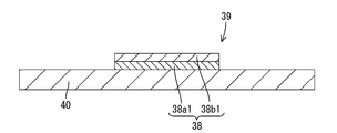
- a cross-sectional view of the main part of the source wiring 38 is shown.
- the step (1) of forming the wiring pattern 39 of the source wiring 38 which is a wet etching method and a wiring pattern forming method according to the first embodiment, is shown.
- a step (2) of forming the wiring pattern 39 of the source wiring 38 is shown.
- a step (3) of forming the wiring pattern 39 of the source wiring 38 is shown.
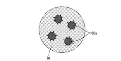
- the figure which expanded a part of compound etching solution 70 is shown.
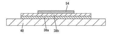
- a step (4) of forming the wiring pattern 39 of the source wiring 38 is shown.
- the figure which expanded a part of compound etching solution 70 at the time of microcapsule 80 destruction is shown.
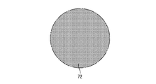
- the figure which expanded a part of mixed etching solution 72 is shown.
- FIG. 1 is a cross-sectional view of a liquid crystal display device 10 according to the first embodiment.
- the upper side shown in FIG. 1 is the front side, and the lower side is the back side.
- the liquid crystal display device 10 includes a liquid crystal panel 11 that is a display panel and a backlight device 12 that is an external light source, and these are integrally held by a bezel 13 that forms a frame shape. It is like that.
- the backlight device 12 is a so-called direct-type backlight in which a light source is arranged directly under the back surface of the liquid crystal panel 11, and has a chassis 14 opened on the front side (light emitting side, liquid crystal panel 11 side), A reflective sheet 15 laid on the optical member 16, an optical member 16 attached to the opening of the chassis 14, a frame 17 for fixing the optical member 16, and a plurality of cold cathodes accommodated in the chassis 14 in parallel.
- the tube 18 is configured to include a lamp holder 19 that shields light from the end of the cold cathode tube 18 and has light reflectivity.
- FIG. 2 shows a cross-sectional view of the liquid crystal panel 11.
- the liquid crystal panel 11 includes a liquid crystal material, which is a substance whose optical characteristics change with application of an electric field, between a pair of transparent (translucent) glass substrates 20 and 30. A liquid crystal layer 29 is enclosed.
- the two substrates 20 and 30 constituting the liquid crystal panel 11 the one disposed on the back side (backlight device 12 side) is the active matrix substrate 30, and the one disposed on the front side (light emitting side) is the CF substrate 20. It is said that.
- FIG. 1 shows a cross-sectional view of the liquid crystal panel 11.
- TFTs Thin Film Transistors
- pixel electrodes 36 which are switching elements. Many are arranged side by side.
- alignment films 25 and 35 for aligning liquid crystal molecules contained in the liquid crystal layer 29 as well as the liquid crystal layer 29 are formed on the inner surfaces of both the substrates 20 and 30, respectively.
- the pretilt angle of the liquid crystal molecules in the liquid crystal layer 29 is controlled by irradiating the alignment films 25 and 35 with ultraviolet rays.
- a pair of front and back polarizing plates 22 are attached to the outer surface sides of both the substrates 20 and 30, respectively.
- the configuration of the CF substrate 20 will be described.
- On the inner surface side of the CF substrate 20 (the liquid crystal layer 29 side and the surface facing the active matrix substrate 30), there is a color filter composed of each colored portion 21 exhibiting R (red), G (green), and B (blue).
- a plurality of the colored portions 21 are arranged in parallel in a matrix at positions that overlap each pixel electrode 36 on the active matrix substrate 30 side, which will be described later, in plan view.
- the light-shielding part (black matrix) 23 which comprises the grid
- the light shielding portion 23 is arranged so as to overlap with a source wiring 38, a gate wiring 32, and a Cs wiring 34 on the active matrix substrate 30 side, which will be described later, in a plan view.
- a counter electrode 26 is provided to face the pixel electrode 36 on the active matrix substrate 30 side.
- the counter electrode is made of a transparent film electrode such as an ITO (Indium Tin Oxide) film, and is formed in a solid shape on the entire surface.
- FIG. 3 shows an enlarged plan view of a part of the active matrix substrate 30.
- the liquid crystal layer 29 side the side facing the CF substrate 20
- many extend along the Y-axis direction (column direction, vertical direction) and are parallel to each other.
- a plurality of source wirings (signal wirings) 38 and a plurality of gate wirings 32 extending in parallel to each other and extending in the X-axis direction (row direction, lateral direction), that is, in a direction orthogonal (crossing) to the source wirings 38.
- a plurality of Cs wirings 34 arranged in parallel with each other while being arranged between the gate wirings 32 and in parallel with the gate wirings 32 are formed in a lattice shape.
- the vertical direction of the drawing is referred to as the column direction
- the horizontal direction of the drawing is referred to as the row direction.
- the gate wiring 32 and the Cs wiring 34 are alternately arranged, and the interval between the adjacent gate wiring 32 and the Cs wiring 34 is set to be approximately equal.
- the source line 38 extends in the column direction along the end of each pixel region (end along the direction orthogonal to the gate line 32), and has a relatively small width with respect to the gate line 32 and the Cs line 34. Is formed.
- the Cs wiring 34 extends in the row direction so as to partially overlap the end portions of the two pixel regions adjacent to each other in the column direction.
- the gate wiring 32 and the Cs wiring 34 are provided by the same material in the same process in the manufacturing process of the active matrix substrate 30 and are arranged in the same layer.
- the gate wiring 32 and the Cs wiring 34 are arranged on the lower layer side relative to the source wiring 38.
- a gate insulating film (not shown) is interposed between the source wiring 38, the gate wiring 32, and the Cs wiring 38 that intersect with each other, so that they are kept in an insulated state.
- an interlayer insulating film (passivation film, protective layer) (not shown) is provided on a further upper layer side of the source wiring 38 relatively disposed on the upper layer side, and the source wiring 38 is protected by this interlayer insulating film. It is illustrated.
- TFTs 37 as switching elements connected to both the wirings 38 and 32 are formed at the intersections of the source wirings 38 and the gate wirings 32, respectively.
- the TFT 37 is a so-called reverse stagger type (bottom gate type), and is disposed on the gate wiring 32.
- a part of the gate wiring 32 is a gate electrode 42.
- the gate electrode 42 is supplied with a scanning signal input to the gate wiring 32 at a predetermined timing.
- a branch line drawn from the source wiring 38 to the TFT 37 side constitutes a source electrode 48 of the TFT 37 that overlaps the gate electrode 42 via a semiconductor film or the like (not shown).
- the image signal (data signal) input to the source wiring 38 is supplied.
- a drain wiring 31 is connected to the pixel electrode 36 through a contact hole 33, and one end side of the drain wiring 31 is drawn to the TFT 37 side and overlapped with a gate electrode 42 via a semiconductor film or the like (not shown). Electrode 41 is formed.
- the drain wiring 31 is provided in the same layer by the same material as the source wiring 38 in the same process, and is provided on the upper layer side relative to the gate wiring 32 and the Cs wiring 34.
- the end of the pixel electrode 36 on the Cs wiring 34 side is disposed so as to overlap the Cs wiring 34 via a gate insulating film and an interlayer insulating film, thereby forming a capacitance with the Cs wiring 34. (See symbol 36a). Thereby, the voltage of the pixel electrode 36 can be held even during a period when the scanning signal is not input to the gate electrode 42 of the TFT 37 (TFT off period).
- the pixel electrode 36 is made of a transparent film electrode such as ITO or ZnO (Zinc Oxide). Note that the active matrix substrate 30 according to the present embodiment employs a so-called multi-pixel driving method in which one pixel region that is a display unit is driven by being divided into two sub-pixels, thereby achieving a favorable viewing angle. The characteristics are realized.
- each of the wirings 32, 38, 31, and 34 are each formed of a metal film patterned on the active matrix substrate 30, and this metal film has a light shielding property.
- each of these wirings is made of a metal material containing copper (Cu), for example, an alloy made of copper and titanium (Ti).
- FIG. 4 shows a cross-sectional view of the main part of the source wiring 38 formed on the glass substrate 40.
- FIG. 4 shows a cross-sectional configuration in which the source wiring 38 is cut along a plane along a direction orthogonal to the direction in which the source wiring 38 extends. As shown in FIG.
- the source wiring 38 of the active matrix substrate 30 is a wiring pattern 39 including a titanium layer 38a1 made of titanium and a copper layer 38b1 made of copper formed on the titanium layer 38a1. Is formed. Since the source wiring 38 has such a configuration, in the source wiring 38, the titanium layer 38a1 functions as a barrier metal. As described above, the titanium layer 38a1 functions as a barrier metal in the source wiring 38, whereby the reliability of the wiring is improved, for example, diffusion of a metal material and mutual reaction are prevented in the source wiring 38.
- the thickness of the titanium layer 38a1 is relatively smaller than the thickness of the copper layer 38b1. Specifically, the thickness of the titanium layer 38a1 is 250 mm, and the thickness of the copper layer 38b1 is 4000 mm. Thus, the wiring layer resistance of the source wiring 38 is reduced because the titanium layer 38a1 that functions as a barrier metal is formed very thin with respect to the copper layer 38b1.
- FIG. 4 a method for forming the wiring pattern 39 of the source wiring 38 shown in FIG. 4 will be described.
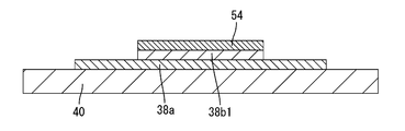
- 5 to 7, 10, and 12 show steps (1) to (5) of forming the wiring pattern 39 of the source wiring 38 in the same cross section as FIG. 4.
- FIG. 10 and FIG. 11 show enlarged views of a part of the composite etching solution 70 (mixed etching solution 72).
- a method for forming the wiring pattern 39 of the source wiring 38 on the glass substrate 40 will be described, but the material for the base can be changed as appropriate. In this method, first, as shown in FIG.
- a titanium film is formed on a glass substrate 40 to a thickness of 250 mm, and a first metal layer 38a (first material) made of titanium (an example of a first material) is formed.
- a first metal layer 38a first material made of titanium (an example of a first material) is formed.
- An example of a layer) (an example of a first layer forming step), and then a copper film having a thickness of 4000 mm is formed on the entire surface of the first metal layer 38a from copper (an example of a second material).
- a second metal layer 38b is formed (an example of a second layer forming step).
- a positive resist resin is applied to the entire surface of the second metal layer 38 a and a part of the glass substrate 40 to form a resist layer 52.
- the resist layer 52 is exposed through a photomask 60 that has been subjected to predetermined patterning. As a result, a portion of the resist layer 52 that overlaps the opening pattern of the photomask 60 is exposed.
- the exposed resist layer 52 is developed. As a result, the exposed portion of the resist layer 52 is removed, and as shown in FIG. 7, a resist pattern 54 is formed on the second metal layer 38a (an example of a resist pattern forming step).
- a composite etching solution 70 shown in FIG. 8 is used as an etching solution.
- FIG. 8 shows an enlarged view of a part of the composite etching solution 70.
- the composite etching solution 70 is a solution in which microcapsules 80 are dispersed in an acetic acid solution (an example of a second etching solution).
- the microcapsule 80 contains a hydrofluoric acid solution (an example of a first etching solution).
- the microcapsule 80 is a known microcapsule that can be broken by applying ultrasonic vibration energy of 20 kHz or higher, and the size, shape, manufacturing method, and the like are not limited.
- a method for including the hydrofluoric acid solution in the microcapsule 80 a known method is used.
- the glass substrate 40 is immersed in the composite etching solution 70.
- a part of the second metal layer 38b is removed by wet etching with an acetic acid solution in the composite etching solution 70 (an example of a first etching process).
- the acetic acid solution can dissolve the second metal layer 38b made of copper and cannot dissolve the first metal layer 38a made of titanium, the first metal layer 38a is not dissolved in the first etching step. Only a part of the second metal layer 38b is removed without being removed. As a result, as shown in FIG.
- the portion overlapping with the resist pattern 54 remains and other portions are removed, and the copper forming a part of the wiring pattern 39 of the source wiring 38 is removed.
- Layer 38b1 is formed. Note that this first etching step is performed without destroying the microcapsules 80.
- FIG. 10 shows an enlarged view of a part of the composite etching solution 70 when the microcapsule 80 is broken.
- FIG. 11 shows an enlarged view of a part of a mixed etching solution 72 described later after the microcapsule 80 is destroyed.
- the timing at which a part of the second metal layer 38b is removed by wet etching can be calculated in advance from the etching rate of copper with respect to the acetic acid solution.
- a known apparatus is used as an apparatus for applying ultrasonic energy of 20 kHz or more to the composite etching solution 70, and a method of applying ultrasonic energy from the outside to the microcapsule 80 is known. This method shall be used.
- the hydrofluoric acid solution flows out of the destroyed microcapsule 80, and the composite etching solution 70 becomes a mixed etching solution 72 of an acetic acid solution and a hydrofluoric acid solution (see FIG. 11).
- a part of the first metal layer 38a is removed by the hydrofluoric acid solution that has flowed out of the broken microcapsule 80 using the resist pattern 54 as a mask. Removal by wet etching (an example of a second etching step). At this time, since the portion of the second metal layer 38b that does not overlap with the resist pattern 54 has already been etched, the hydrofluoric acid solution is prevented or suppressed from adversely affecting the second metal layer 38b such as corrosion. Is done. As a result, as shown in FIG. 12, a portion of the first metal layer 38 b that overlaps with the resist pattern 54 remains and other portions are removed, and titanium forming a part of the wiring pattern 39 of the source wiring 38 is formed. Layer 38a1 is formed.
- the glass substrate 40 is removed from the mixed etching solution 72 at a timing at which a part of the first metal layer 38a is removed by wet etching (specifically, around 15 seconds after the second etching step is started).
- the resist pattern 54 is removed by ashing (an example of an ashing process). Note that the timing at which a part of the first metal layer 38a is removed by wet etching can be calculated in advance from the etching rate of titanium with respect to the hydrofluoric acid solution.
- the second metal layer 38b is changed to the hydrofluoric acid solution in the first etching step. Exposure can be prevented. Furthermore, since the acetic acid solution cannot dissolve the first metal layer 38a made of titanium, it is possible to prevent the first metal layer 38a from being etched in the first etching step. In the second etching step, since part of the second metal layer 38b has already been etched, only the first metal layer 38a is etched by the hydrofluoric acid solution. For this reason, it is possible to prevent or suppress the hydrofluoric acid solution from affecting the second metal layer 38b.
- first metal layer 38a and second metal layer 38b are successively wet-etched with different etching solutions (hydrofluoric acid solution and acetic acid solution), one etching is performed. It is possible to prevent or suppress the solution (hydrofluoric acid solution) from affecting one layer (second metal layer 38b).
- the hydrofluoric acid solution is a strong acid
- the second metal layer 38b made of copper is in contact with the hydrofluoric acid solution for a long time, disconnection due to excessive etching of the second metal layer 38b or two metal layers. Differences in wiring width between the layers 38a and 38b, corrosion of the second metal layer 38b due to oxidation of the copper surface, and the like may occur.
- the wet etching method according to the present embodiment it is possible to prevent or suppress the hydrofluoric acid solution from exerting such an adverse effect on the second metal layer 38b.
- etching a part of each of the two laminated metal layers 38a and 38b a method of removing one metal layer by wet etching and removing the other metal layer by dry etching is conceivable.
- at least two etching apparatuses are required to perform wet etching and dry etching, respectively, and the cost increases.
- a part of the stacked two metal layers 38a and 38b can be removed by wet etching using one etching apparatus, so that the cost can be reduced. it can.
- the two metal layers 38a and 38b cannot be continuously etched by the above-described method using both wet etching and dry etching.
- the wet etching method according to the present embodiment the two metal layers 38a and 38b are continuously etched by destroying the microcapsule 80 in a state where the glass substrate 40 is immersed in the composite etching solution 70. Can do. Therefore, etching can be performed in a short time, and the work process can be shortened.
- the destruction process is performed at a timing when a part of the second metal layer 38b is removed by wet etching.
- the hydrofluoric acid solution flows out of the microcapsule 80 after a part of the second metal layer 38b is completely removed, so that the hydrofluoric acid solution affects the second metal layer 38b. Can be effectively prevented or suppressed.
- the microcapsule 80 is a microcapsule 80 that can be broken by ultrasonic vibration energy.
- the breaking step the microcapsule 80 is broken by applying ultrasonic vibration energy to the microcapsule 80 from the outside to vibrate the microcapsule 80 at the resonance frequency. For this reason, in the destruction step, a specific configuration for breaking the microcapsule 80 can be realized, and the microcapsule 80 can be broken from the outside.
- ultrasonic vibration energy of 20 kHz or more is applied to the microcapsule 80 in the destruction process. For this reason, the microcapsule 80 can be effectively broken by the ultrasonic vibration energy in the breaking step.
- the copper constituting the second metal layer 38b can be prevented from being exposed to the hydrofluoric acid solution in the first etching step, and the first The metal layer 38a can be prevented from being etched.
- the second etching step only titanium constituting the first metal layer 38a is etched by the hydrofluoric acid solution. For this reason, it is possible to prevent or suppress the hydrofluoric acid solution from affecting the copper constituting the second metal layer 38b, and to form a good wiring pattern 39 in which disconnection or the like of the second metal layer 38b is prevented. Can be formed.
- titanium is used as the first metal material in the first layer forming step
- copper is used as the second metal material in the second layer forming step. Is used.
- the microcapsule 80 including the hydrofluoric acid solution as the first etching solution is contained in the composite etching solution 70 dispersed in the acetic acid solution or the nitric acid solution as the second etching solution.
- the glass substrate 40 is immersed. Therefore, it is possible to prevent or suppress the hydrofluoric acid solution from affecting the copper in the first etching step and the second etching step, and to prevent or suppress the copper surface from being oxidized by the hydrofluoric acid solution. Can do.
- the second metal layer 38b having a relatively larger thickness than the first metal layer 38a is formed in the second layer forming step.
- the first metal layer 38a functions as a barrier metal for the second metal layer 38b, and the first metal layer 38a is relatively thinner than the second metal layer 38b.
- the wiring resistance of 38 can be reduced.
- the first metal layer 38a is formed with a thickness of 250 mm in the first forming step, and the first metal layer 38a is formed with a thickness of 4000 mm in the second forming step.
- the second metal layer 38b is formed.
- the first etching process is performed for about 100 seconds, and the second etching process is performed for about 15 seconds.
- the time for performing the second etching step is the first etching time. Since the time is much shorter than the time for performing the time, it is possible to suppress the hydrofluoric acid solution from affecting the second metal layer 38b.
- the first modification of the first embodiment is different from the method according to the first embodiment in the configuration of the microcapsule 80 and the method for destroying the microcapsule 80.
- the microcapsule 80 is a known microcapsule that can be destroyed by irradiation with laser light.
- the wavelength of the laser beam that can break the microcapsule 80 can be arbitrarily changed according to the use mode.
- the microcapsule 80 is broken by irradiating the microcapsule 80 with a YAG laser in the breaking step.
- the wavelength of the YAG laser can be 355 nm, 532 nm, or 1064 nm.
- the microcapsule 80 can be destroyed from the outside using a YAG laser.
- the configuration of the microcapsule 80 is the same as that according to the first modification, and the type of laser light for destroying the microcapsule 80 is different from that according to the first modification. ing.
- the microcapsule 80 is destroyed by irradiating the microcapsule 80 with an excimer laser.
- the wavelength of the excimer laser can be 193 nm, 248 nm, 308 nm, or 351 nm.
- the microcapsule 80 can be destroyed from the outside using an excimer laser.
- the second embodiment relates to a method for manufacturing the active matrix substrate 30 by the method for forming the wiring pattern 39 described in the first embodiment. Since the configuration of the active matrix substrate 30 and the configuration of the liquid crystal display device 10 are the same as those of the first embodiment, the description of the structure, operation, and effects is omitted.
- the wiring patterns of the source electrode 48 and the drain electrode 41 are formed in the region where the TFT 37 is formed by the method of forming the wiring pattern 39 described in the first embodiment. Further, before and after the formation of these wiring patterns, a gate insulating film, an interlayer insulating film, a pixel electrode, and the like constituting the active matrix substrate 30 are formed. As described above, the active matrix substrate 30 is manufactured.
- the thin film transistors are formed with a good wiring pattern in which the corrosion or disconnection of the wiring is prevented or suppressed with respect to the plurality of TFTs 37 formed in a plurality of locations of the active matrix substrate 30. Since it can be formed, the active matrix substrate 30 with high reliability can be manufactured.
- a hydrofluoric acid solution is used as the first etching solution
- an acetic acid solution is used as the second etching solution.
- the materials of the first etching solution and the second etching solution are limited.
- a nitric acid solution may be used as the second etching solution.
- a mixed solution of an acetic acid solution and a nitric acid solution may be used as the second etching solution.
- a method using a microcapsule that can be broken by applying ultrasonic vibration energy from the outside or irradiating a laser beam from the outside is exemplified.
- the method of destroying a microcapsule is not limited.
- a microcapsule that can be broken by applying thermal energy from the outside may be used, and the microcapsule may be broken by thermal energy.
- a first layer is formed by forming titanium with a thickness of 250 mm in the first layer forming step, and a copper film is formed with a thickness of 4000 mm in the second layer forming step.
- the method of forming the second layer has been exemplified, the material, thickness, and the like constituting the first layer and the second layer are not limited.
- a method of forming a wiring pattern on an inverted stagger type (bottom gate type) active matrix substrate is exemplified.
- a wiring pattern is formed on a stagger type (up gate type) active matrix substrate. May be formed.
- the method of forming the wiring pattern on the active matrix substrate configured by the multi-pixel driving method is exemplified.
- the wiring is formed on a normal active matrix substrate (without subpixels). A pattern may be formed.
Landscapes
- Chemical & Material Sciences (AREA)
- Chemical Kinetics & Catalysis (AREA)
- General Chemical & Material Sciences (AREA)
- Engineering & Computer Science (AREA)
- Materials Engineering (AREA)
- Mechanical Engineering (AREA)
- Metallurgy (AREA)
- Organic Chemistry (AREA)
- Liquid Crystal (AREA)
- Thin Film Transistor (AREA)
Abstract
本発明に係るエッチング方法は、フッ酸溶液が包含されたマイクロカプセル80が酢酸溶液中に分散された複合エッチング溶液70を用いてエッチングを行う方法であって、基板上にチタンを成膜して第1の層を形成する工程と、チタン層上に銅を成膜して第2の層を形成する工程と、基板を複合エッチング溶液70中に浸漬させ、マイクロカプセル80を破壊させることなく、酢酸溶液によって銅の一部をウェットエッチングにより除去する工程と、ガラス基板を複合エッチング溶液中に浸漬させた状態でマイクロカプセル80を破壊する工程と、破壊されたマイクロカプセル80内から流出したフッ酸溶液によってチタン層の一部をウェットエッチングにより除去する工程とを備える。
Description
本発明は、ウェットエッチング方法、配線パターンの形成方法、及びアクティブマトリクス基板の製造方法に関する。
液晶表示装置に用いられる液晶パネルは、一対のガラス基板の間に液晶層が挟持された構成とされており、そのうち一方のガラス基板は、アクティブ素子としてTFT(Thin Film Transistor、薄膜トランジスタ)を備えたアクティブマトリクス基板とされる。
このようなアクティブマトリクス基板は、下地層上にレジストパターンを形成し、フォトリソグラフィー技術を利用して露光、現像、及びエッチング工程を複数回繰り返すことによって製造する。即ち、アクティブマトリクス基板を形成するゲート配線、ゲート絶縁膜、ソース配線、ドレイン配線等の配線パターンや、半導体層、層間絶縁膜、画素電極等をそれぞれ露光、現像、及びエッチング工程等を繰り返すことで順次積層していくものである。このうちエッチング工程においては、配線のパターニング精度がトランジスタの性能に影響を及ぼすため、慎重に行う必要がある。
特許文献1に、エッチング溶液が包含されたマイクロカプセルを利用してウェットエッチングを行うエッチング方法が開示されている。このエッチング方法では、エッチング溶液が包含されたマイクロカプセルを金属層が形成された基板の表面上にパターニングした後に、マイクロカプセルを熱等により破壊し、マイクロカプセルから放出されたエッチング溶液を用いてパターニングした部位の金属層をエッチングする。これにより、基板上に形成された単一の層の一部をウェットエッチングにより精度良く除去することができる。
(発明が解決しようとする課題)
特許文献1のエッチング方法では、例えば基板上に2つの層が積層されている場合、各層の一部を連続してウェットエッチングするために、一方の層をエッチングするための溶液と他方の層をエッチングするための溶液との混合溶液をエッチング溶液として用いる必要がある。しかしながら、このようなエッチング溶液を用いた場合、一方の層をエッチングする工程において、一方の層をエッチングするための溶液がエッチング対象でない他方の層に対して影響を及ぼすことがある。この場合、他方の層において断線や腐食等が発生することがある。
特許文献1のエッチング方法では、例えば基板上に2つの層が積層されている場合、各層の一部を連続してウェットエッチングするために、一方の層をエッチングするための溶液と他方の層をエッチングするための溶液との混合溶液をエッチング溶液として用いる必要がある。しかしながら、このようなエッチング溶液を用いた場合、一方の層をエッチングする工程において、一方の層をエッチングするための溶液がエッチング対象でない他方の層に対して影響を及ぼすことがある。この場合、他方の層において断線や腐食等が発生することがある。
本発明は、上記の問題に鑑みて創作されたものである。本発明は、積層された2つの層を異なるエッチング溶液で連続してウェットエッチングする場合に、一方のエッチング溶液が一方の層に影響を及ぼすことを防止ないし抑制することができるウェットエッチング方法を提供することを目的とする。さらに、そのようなウェットエッチング方法を用いて配線パターンを形成する方法を提供することを目的とする。ひいては、そのような配線パターンの形成方法を用いてアクティブマトリクス基板を製造する方法を提供することをも目的とする。
(課題を解決するための手段)
本発明の第1の態様は、第1の材料を溶解可能な第1のエッチング溶液が包含されたマイクロカプセルが、第2の材料を溶解可能であって前記第1の材料を溶解不能な第2のエッチング溶液中に分散された複合エッチング溶液を用いてウェットエッチングを行う方法であって、下地層上に前記第1の材料を成膜して第1の層を形成する第1層形成工程と、該第1の層上に前記第2の材料を成膜して第2の層を形成する第2層形成工程と、前記下地層を前記複合エッチング溶液中に浸漬させ、マスクを介して、前記マイクロカプセルを破壊させることなく、前記第2のエッチング溶液によって前記第2の層の一部をウェットエッチングにより除去する第1エッチング工程と、該第1エッチング工程の後に、前記下地層を前記複合エッチング溶液中に浸漬させた状態で前記マイクロカプセルを破壊する破壊工程と、該破壊工程の後に、マスクを介して、破壊された前記マイクロカプセル内から流出した前記第1のエッチング溶液によって前記第1の層の一部をウェットエッチングにより除去する第2エッチング工程と、を備えるウェットエッチング方法に関する。
本発明の第1の態様は、第1の材料を溶解可能な第1のエッチング溶液が包含されたマイクロカプセルが、第2の材料を溶解可能であって前記第1の材料を溶解不能な第2のエッチング溶液中に分散された複合エッチング溶液を用いてウェットエッチングを行う方法であって、下地層上に前記第1の材料を成膜して第1の層を形成する第1層形成工程と、該第1の層上に前記第2の材料を成膜して第2の層を形成する第2層形成工程と、前記下地層を前記複合エッチング溶液中に浸漬させ、マスクを介して、前記マイクロカプセルを破壊させることなく、前記第2のエッチング溶液によって前記第2の層の一部をウェットエッチングにより除去する第1エッチング工程と、該第1エッチング工程の後に、前記下地層を前記複合エッチング溶液中に浸漬させた状態で前記マイクロカプセルを破壊する破壊工程と、該破壊工程の後に、マスクを介して、破壊された前記マイクロカプセル内から流出した前記第1のエッチング溶液によって前記第1の層の一部をウェットエッチングにより除去する第2エッチング工程と、を備えるウェットエッチング方法に関する。
上記のウェットエッチング方法によると、第1エッチング工程では第1のエッチング溶液がマイクロカプセル内に包含されているので、第1エッチング工程において第2の層が第1のエッチング溶液に晒されることを防止することができる。さらに、第2のエッチング溶液は第1の層を溶解不能なので、第1エッチング工程において第1の層がエッチングされることを防止することができる。そして、第2エッチング工程では、第2の層の一部が既にエッチングされているので、第1のエッチング溶液によって第1の層のみがエッチングされることとなる。このため、第1のエッチング溶液が第2の層に影響を及ぼすことを防止ないし抑制することができる。このように、積層された2つの層を異なるエッチング溶液で連続してウェットエッチングする場合に、一方のエッチング溶液が一方の層に影響を及ぼすことを防止ないし抑制することができる。
前記破壊工程は、前記第2の層の一部がウェットエッチングにより除去されたタイミングで行ってもよい。
この方法によると、第2の層の一部が完全に除去された後に第1のエッチング溶液がマイクロカプセル内から流出することとなるので、第1のエッチング溶液が第2の層に影響を及ぼすことを効果的に防止ないし抑制することができる。なお、第2の層の一部がウェットエッチングにより除去されるタイミングは、例えば第2のエッチング溶液に対する第2の層のエッチングレートから予め算出することができる。
この方法によると、第2の層の一部が完全に除去された後に第1のエッチング溶液がマイクロカプセル内から流出することとなるので、第1のエッチング溶液が第2の層に影響を及ぼすことを効果的に防止ないし抑制することができる。なお、第2の層の一部がウェットエッチングにより除去されるタイミングは、例えば第2のエッチング溶液に対する第2の層のエッチングレートから予め算出することができる。
前記マイクロカプセルが、超音波振動エネルギーによって破壊可能なマイクロカプセルであって、前記破壊工程では、前記マイクロカプセルに対して前記超音波振動エネルギーを外部から付与して前記マイクロカプセルを共振周波数で振動させることで該マイクロカプセルを破壊してもよい。
この方法によると、破壊工程において、マイクロカプセルを破壊するための具体的な構成を実現することができると共に、マイクロカプセルを外部から破壊することができる。
この方法によると、破壊工程において、マイクロカプセルを破壊するための具体的な構成を実現することができると共に、マイクロカプセルを外部から破壊することができる。
前記破壊工程では、前記マイクロカプセルに対して20kHz以上の前記超音波振動エネルギーを付与してもよい。
この方法によると、破壊工程において、超音波振動エネルギーによってマイクロカプセルを破壊するための具体的な構成を実現することができる。
この方法によると、破壊工程において、超音波振動エネルギーによってマイクロカプセルを破壊するための具体的な構成を実現することができる。
前記マイクロカプセルが、レーザ光によって破壊可能なマイクロカプセルであって、前記破壊工程では、前記マイクロカプセルに対して前記レーザ光を外部から照射して前記マイクロカプセルを破壊してもよい。
この方法によると、破壊工程において、マイクロカプセルを破壊するための具体的構成を実現することができると共に、マイクロカプセルを外部から破壊することができる。
この方法によると、破壊工程において、マイクロカプセルを破壊するための具体的構成を実現することができると共に、マイクロカプセルを外部から破壊することができる。
前記破壊工程では、前記マイクロカプセルに対してレーザ光としてYAGレーザを照射してもよい。
この方法によると、破壊工程において、レーザ光によってマイクロカプセルを破壊するための具体的な構成を実現することができる。
この方法によると、破壊工程において、レーザ光によってマイクロカプセルを破壊するための具体的な構成を実現することができる。
前記破壊工程では、前記マイクロカプセルに対してレーザ光としてエキシマレーザを照射してもよい。
この方法によると、破壊工程において、レーザ光によってマイクロカプセルを破壊するための具体的な構成を実現することができる。
この方法によると、破壊工程において、レーザ光によってマイクロカプセルを破壊するための具体的な構成を実現することができる。
本発明の第2の態様は、上記のウェットエッチング方法を用いて配線パターンを形成する方法であって、前記第1エッチング工程の前に、前記第2の層上にレジストパターンを形成するレジストパターン形成工程と、前記第2エッチング工程の後に、前記レジストパターンをアッシングにより除去するアッシング工程と、をさらに備え、前記第1層形成工程では、前記下地層として基板を用いると共に、前記第1の材料として第1の金属材料を用い、前記第2層形成工程では、前記第2の材料として第2の金属材料を用い、前記第1エッチング工程では、前記レジストパターンをマスクとして前記第2の層の一部をウェットエッチングにより除去し、前記第2エッチング工程では、前記レジストパターンをマスクとして前記第1の層の一部をウェットエッチングにより除去する配線パターンの形成方法に関する。
上記の配線パターンの形成方法によると、第1エッチング工程において、第2の層を構成する第2の金属材料が第1のエッチング溶液に晒されることを防止できると共に、第1の層がエッチングされることを防止することができる。そして、第2エッチング工程では、第1のエッチング溶液によって第1の層を構成する第1の金属材料のみがエッチングされることとなる。このため、第1のエッチング溶液が第2の層を構成する第2の金属材料に影響を及ぼすことを防止ないし抑制することができ、第2の層の断線等が防止された良好な配線パターンを形成することができる。
前記第1層形成工程では、前記第1の金属材料としてチタンを用い、前記第2層形成工程では、前記第2の金属材料として銅を用い、前記第1エッチング工程では、前記第1のエッチング溶液としてのフッ酸溶液が包含されたマイクロカプセルが、前記第2のエッチング溶液としての酢酸溶液又は硝酸溶液中に分散された前記複合エッチング溶液中に前記基板を浸漬させてもよい。
この方法によると、第1エッチング工程及び第2エッチング工程においてフッ酸溶液が銅に影響を及ぼすことを防止ないし抑制することができる。このため、銅の表面がフッ酸溶液によって酸化等することを防止ないし抑制することができる。
この方法によると、第1エッチング工程及び第2エッチング工程においてフッ酸溶液が銅に影響を及ぼすことを防止ないし抑制することができる。このため、銅の表面がフッ酸溶液によって酸化等することを防止ないし抑制することができる。
前記第2層形成工程では、前記第1の層よりも相対的に厚みが大きな前記第2の層を形成してもよい。
この方法によると、第1の層が第2の層に対するバリアメタルとして機能しながら第1の層が第2の層よりも相対的に膜厚が薄くなることで、配線パターンの形成後における配線の抵抗を低減することができる。
この方法によると、第1の層が第2の層に対するバリアメタルとして機能しながら第1の層が第2の層よりも相対的に膜厚が薄くなることで、配線パターンの形成後における配線の抵抗を低減することができる。
前記第1層形成工程では、250~500Åの範囲内の厚みで前記第1の層を形成し、前記第2層形成工程では、2800~4000Åの範囲内の厚みで前記第2の層を形成してもよい。
この方法によると、配線パターンの形成後における配線の抵抗を低減するための具体的な構成が実現された配線パターンを形成することができる。
この方法によると、配線パターンの形成後における配線の抵抗を低減するための具体的な構成が実現された配線パターンを形成することができる。
前記第1形成工程では、250Åの厚みで前記第1の層を形成し、前記第2形成工程では、4000Åの厚みで前記第2の層を形成し、前記第1のエッチング工程は約100秒間行い、前記第2のエッチング工程は約15秒間行ってもよい。
この方法によると、第1エッチング工程における第2の層のエッチングが完了するのとほぼ同時に破壊工程に移行することができ、さらに、第2エッチング工程における第1の層のエッチングが完了するのとほぼ同時にアッシング工程に移行することができる。このため、第1のエッチング溶液が第2の層に影響を及ぼすことを効果的に防止ないし抑制することができる。
この方法によると、第1エッチング工程における第2の層のエッチングが完了するのとほぼ同時に破壊工程に移行することができ、さらに、第2エッチング工程における第1の層のエッチングが完了するのとほぼ同時にアッシング工程に移行することができる。このため、第1のエッチング溶液が第2の層に影響を及ぼすことを効果的に防止ないし抑制することができる。
本発明の第3の態様は、基板と、該基板上に形成された複数の薄膜トランジスタと、を備えるアクティブマトリクス基板を製造する方法であって、前記基板上の前記薄膜トランジスタが形成される領域に上記の配線パターンの形成方法によって配線パターンを形成する工程を備えるアクティブマトリクス基板の製造方法に関する。
上記のアクティブマトリクス基板の製造方法によると、配線の腐食や断線等が防止ないし抑制された良好な配線パターンで薄膜トランジスタを形成することができるので、信頼性の高いアクティブマトリクス基板を製造することができる。
(発明の効果)
本発明によれば、積層された2つの異なる層を2つの異なるエッチング溶液で連続してウェットエッチングする場合に、一方のエッチング溶液が一方の層に影響を及ぼすことを防止ないし抑制することができる。さらに、そのようなウェットエッチング方法を用いて配線パターンを形成することができる。ひいては、そのような配線パターンを用いてアクティブマトリクス基板を製造することもできる。
本発明によれば、積層された2つの異なる層を2つの異なるエッチング溶液で連続してウェットエッチングする場合に、一方のエッチング溶液が一方の層に影響を及ぼすことを防止ないし抑制することができる。さらに、そのようなウェットエッチング方法を用いて配線パターンを形成することができる。ひいては、そのような配線パターンを用いてアクティブマトリクス基板を製造することもできる。
<実施形態1>
図面を参照して実施形態1を説明する。図1は、実施形態1に係る液晶表示装置10の断面図を示している。ここで、図1に示す上側を表側とし、同図下側を裏側とする。液晶表示装置10は、図1に示すように、表示パネルである液晶パネル11と、外部光源であるバックライト装置12とを備え、これらが枠状を成すベゼル13などにより一体的に保持されるようになっている。
図面を参照して実施形態1を説明する。図1は、実施形態1に係る液晶表示装置10の断面図を示している。ここで、図1に示す上側を表側とし、同図下側を裏側とする。液晶表示装置10は、図1に示すように、表示パネルである液晶パネル11と、外部光源であるバックライト装置12とを備え、これらが枠状を成すベゼル13などにより一体的に保持されるようになっている。
まず、バックライト装置12の構成の概略について説明する。バックライト装置12は、液晶パネル11の背面直下に光源が配されてなる、いわゆる直下型のバックライトであり、表側(光出射側、液晶パネル11側)に開口したシャーシ14と、シャーシ14内に敷設される反射シート15と、シャーシ14の開口部分に取り付けられる光学部材16と、光学部材16を固定するためのフレーム17と、シャーシ14内に並列した状態で収容される複数本の冷陰極管18と、冷陰極管18の端部を遮光すると共に自身が光反射性を備えてなるランプホルダ19と、を有して構成されている。
続いて、液晶パネル11の構成の概略について説明する。図2は、液晶パネル11の断面図を示している。液晶パネル11は、図2に示すように、一対の透明な(透光性を有する)ガラス製の基板20,30間に、電界印加に伴って光学特性が変化する物質である液晶材料を含む液晶層29を封入してなる。液晶パネル11を構成する両基板20,30のうち裏側(バックライト装置12側)に配されるものがアクティブマトリクス基板30とされ、表側(光出射側)に配されるものが、CF基板20とされている。アクティブマトリクス基板30における内面側(液晶層29側、CF基板20との対向面側)には、図2に示すように、スイッチング素子であるTFT(Thin Film Transistor、薄膜トランジスタ)37及び画素電極36が多数並んで設けられている。また、両基板20,30の内面側には、液晶層29に臨むと共に液晶層29に含まれる液晶分子を配向させるための配向膜25、35がそれぞれ形成されている。液晶パネル11では、これらの配向膜25、35に紫外線を照射することで液晶層29内の液晶分子のプレチルト角を制御する。なお、両基板20,30の外面側には、表裏一対の偏光板22がそれぞれ貼り付けられている。
先に、CF基板20の構成について説明する。CF基板20における内面側(液晶層29側、アクティブマトリクス基板30との対向面側)には、R(赤色)、G(緑色)、B(青色)を呈する各着色部21から成るカラーフィルタが設けられており、各着色部21は、後述するアクティブマトリクス基板30側の各画素電極36と平面視において重畳する位置に多数個がマトリクス状に並列配置されている。カラーフィルタを構成する各着色部間には、混色を防ぐための格子状を成す遮光部(ブラックマトリクス)23が形成されている。遮光部23は、後述するアクティブマトリクス基板30側のソース配線38、ゲート配線32及びCs配線34に対して平面視において重畳する配置とされている。各着色部21及び遮光部23の表面には、アクティブマトリクス基板30側の画素電極36と対向する対向電極26が設けられている。対向電極は、例えばITO(Indium Tin Oxide)膜等の透明膜電極から成り、全面ベタ状に形成されている。
続いて、アクティブマトリクス基板30の構成について説明する。図3は、アクティブマトリクス基板30の一部を拡大した平面図を示している。アクティブマトリクス基板30における内面側(液晶層29側、CF基板20との対面側)には、図3に示すように、Y軸方向(列方向、縦方向)に沿って延びると共に互いに並列する多数本のソース配線(信号配線)38と、X軸方向(行方向、横方向)、即ちソース配線38に対して直交(交差)する方向に沿って延びると共に互いに並列する多数本のゲート配線32と、各ゲート配線32間に配されると共にゲート配線32に並行しつつ互いに並列する多数本のCs配線34とが格子状に形成されている。なお、以下では、平面図又は裏面図において図の上下方向を列方向と称し、図の左右方向を行方向と称することとする。
ゲート配線32とCs配線34とは交互に配されており、隣り合うゲート配線32とCs配線34との間の間隔はほぼ等しく設定されている。ソース配線38は各画素領域の端部(ゲート配線32と直交する方向に沿った端部)に沿って列方向に延びており、ゲート配線32及びCs配線34に対して相対的に小さな幅で形成されている。Cs配線34はそれぞれ列方向に隣接する2つの画素領域それぞれの端部と一部が重なるように行方向に延びている。ゲート配線32及びCs配線34は、アクティブマトリクス基板30の製造工程において共に同一工程にて同一材料によって設けられており、同一の層に配されている。ゲート配線32及びCs配線34は、ソース配線38に対して相対的に下層側に配されている。互いに交差するソース配線38とゲート配線32、Cs配線38との間には、図示しないゲート絶縁膜が介在しており、それにより相互が絶縁状態に保たれている。また、相対的に上層側に配されるソース配線38のさらに上層側には、図示しない層間絶縁膜(パッシベーション膜、保護層)が設けられており、この層間絶縁膜によりソース配線38の保護が図られている。
各ソース配線38と各ゲート配線32との交差部には、図3に示すように、両配線38、32に接続されるスイッチング素子としてのTFT37がそれぞれ形成されている。TFT37は、いわゆる逆スタガ型(ボトムゲート型)であって、ゲート配線32上に配置されている。そして、ゲート配線32の一部は、ゲート電極42となっている。このゲート電極42には、所定のタイミングでゲート配線32に入力される走査信号が供給されるようになっている。また、ソース配線38からTFT37側に引き出された枝線がゲート電極42に対して半導体膜等(図示せず)を介して重畳するTFT37のソース電極48を構成しており、このソース電極48には、ソース配線38に入力される画像信号(データ信号)が供給されるようになっている。
ソース配線38、ゲート配線32及びCs配線34によって囲まれた領域には、図3に示すように、縦長の方形状をなす画素電極36がマトリクス状に多数並んで配されている。画素電極36には、コンタクトホール33を介してドレイン配線31が接続され、このドレイン配線31の一端側がTFT37側に引き出されてゲート電極42と半導体膜等(図示せず)を介して重畳するドレイン電極41となっている。このドレイン配線31は、ソース配線38と同一材料により同一工程にて同一の層に設けられており、ゲート配線32及びCs配線34に対して相対的に上層側に設けられている。画素電極36のうちCs配線34側の端部は、Cs配線34に対してゲート絶縁膜及び層間絶縁膜を介して重畳配置されることで、Cs配線34との間で容量を形成している(符号36a参照)。これにより、TFT37のゲート電極42に走査信号が入力されない期間(TFTオフ期間)においても、画素電極36の電圧を保持することが可能とされる。また、画素電極36は、ITO或いはZnO(Zinc Oxide)等の透明膜電極から成っている。なお、本実施形態に係るアクティブマトリクス基板30では、表示単位である1つの画素領域を2つの副画素に分割して駆動するいわゆるマルチ画素駆動方式を採用しており、これにより、良好な視野角特性が実現されている。
続いて、上述した各配線32、38、31、34の構成について説明する。ゲート配線32、ソース配線38、ドレイン配線31及びCs配線34は、アクティブマトリクス基板30上にそれぞれパターニングされた金属膜から成り、この金属膜は遮光性を有している。具体的には、これらの配線は、いずれも銅(Cu)を含む金属材料からなり、例えば銅及びチタン(Ti)から成る合金から成るものとされる。ここで、図4に、ガラス基板40上に形成されたソース配線38の要部断面図を示す。図4は、ソース配線38を当該ソース配線38が延びる方向と直交する方向に沿った面で切断した断面構成を示している。本実施形態に係るアクティブマトリクス基板30のソース配線38は、図4に示すように、チタンから成るチタン層38a1とチタン層38a1上に形成された銅から成る銅層38b1とから成る配線パターン39で形成されている。ソース配線38がこのような構成とされていることで、ソース配線38では、チタン層38a1がバリアメタルとしての機能を果たしている。このようにソース配線38においてチタン層38a1がバリアメタルとして機能することで、ソース配線38において金属材料の拡散や相互反応が防止される等、配線の信頼性が向上されている。
また、ソース配線38では、チタン層38a1の厚みが銅層38b1の厚みよりも相対的に小さいものとなっている。具体的には、チタン層38a1の厚みは250Åとなっており、銅層38b1の厚みは4000Åとなっている。このように、銅層38b1に対してバリアメタルとして機能するチタン層38a1が非常に薄く形成されていることで、ソース配線38の配線抵抗が低減されている。
続いて、図4に示したソース配線38の配線パターン39を形成する方法について説明する。図5~図7、図10、図12は、図4と同一の断面において、ソース配線38の配線パターン39を形成する工程(1)~(5)を示している。また、図8、図10、図11は、複合エッチング溶液70(混合エッチング溶液72)の一部を拡大した図を示している。なお、以下では、ガラス基板40上にソース配線38の配線パターン39を形成する方法について説明するが、下地とする材料については適宜に変更可能である。本方法では、まず、図5に示すように、ガラス基板40上にチタン膜を250Åの厚みで成膜してチタン(第1の材料の一例)から成る第1の金属層38a(第1の層の一例)を形成し(第1層形成工程の一例)、次いで、第1の金属層38a上の全面に銅膜を4000Åの厚みで成膜して銅(第2の材料の一例)から成る第2の金属層38b(第2の層の一例)を形成する(第2層形成工程の一例)。
次いで、図6に示すように、第2の金属層38a上の全面及びガラス基板40の一部にポジ型のレジスト樹脂を塗布してレジスト層52を形成する。次いで、図6に示すように、所定のパターニングがされたフォトマスク60を介して、レジスト層52に対して露光を行う。これにより、レジスト層52のうち、フォトマスク60の開口パターンと重畳する部位が感光する。次いで、露光されたレジスト層52の現像を行う。これにより、レジスト層52のうち感光した部位が取り除かれ、図7に示すように、第2の金属層38a上にレジストパターン54が形成される(レジストパターン形成工程の一例)。
続いて、形成したレジストパターン54をマスクとして第1の金属層38a及び第2の金属層38bのウェットエッチングを行うが、このときエッチング溶液として図8に示す複合エッチング溶液70を用いる。ここで、図8は、複合エッチング溶液70の一部を拡大した図を示している。この複合エッチング溶液70は、図8に示すように、酢酸溶液(第2のエッチング溶液の一例)中にマイクロカプセル80が分散された溶液である。マイクロカプセル80内には、フッ酸溶液(第1のエッチング溶液の一例)が包含されている。なお、マイクロカプセル80は、20kHz以上の超音波振動エネルギーを付与することで破壊可能な公知のマイクロカプセルとされており、大きさ、形状、製造方法等は限定されない。また、マイクロカプセル80内にフッ酸溶液を包含させる方法については、公知の方法を利用するものとする。
次いで、ガラス基板40をこの複合エッチング溶液70中に浸漬させる。そして、レジストパターン54をマスクとして、複合エッチング溶液70中の酢酸溶液によって第2の金属層38bの一部をウェットエッチングにより除去する(第1エッチング工程の一例)。ここで、酢酸溶液は、銅から成る第2の金属層38bを溶解可能であってチタンから成る第1の金属層38aを溶解不能であるので、第1エッチング工程では、第1の金属層38aが除去されることなく第2の金属層38bの一部のみが除去される。これにより、図9に示すように、第2の金属層38bのうち、レジストパターン54と重畳する部位が残存すると共にその他の部位が除去され、ソース配線38の配線パターン39の一部を成す銅層38b1が形成される。なお、この第1エッチング工程は、マイクロカプセル80を破壊させることなく行うものとする。
次いで、第2の金属層38bの一部がウェットエッチングにより除去されるタイミング(具体的には、第1エッチング工程を開始してから100秒前後)で、外部から複合エッチング溶液70に対して20kHz以上の超音波エネルギーを付与する。これにより、複合エッチング溶液70中に分散されたマイクロカプセル80を共振周波数で振動させ、図10に示すように、マイクロカプセル80を破壊する(破壊工程の一例)。ここで、図10は、マイクロカプセル80が破壊されるときの複合エッチング溶液70の一部を拡大した図を示している。また、図11は、マイクロカプセル80が破壊された後の後述する混合エッチング溶液72の一部を拡大した図を示している。なお、この破壊工程において、第2の金属層38bの一部がウェットエッチングにより除去されるタイミングは、酢酸溶液に対する銅のエッチングレートから予め算出することができる。また、複合エッチング溶液70に対して20kHz以上の超音波エネルギーを付与するための装置については公知の装置を利用するものとし、マイクロカプセル80に対して外部から超音波エネルギーを付与する方法については公知の方法を利用するものとする。この破壊工程により、破壊されたマイクロカプセル80内からフッ酸溶液が流出し、複合エッチング溶液70は酢酸溶液とフッ酸溶液との混合エッチング溶液72となる(図11参照)。
次いで、ガラス基板40をこの混合エッチング溶液72中に浸漬させた状態で、レジストパターン54をマスクとして、破壊されたマイクロカプセル80内から流出したフッ酸溶液によって第1の金属層38aの一部をウェットエッチングにより除去する(第2エッチング工程の一例)。このとき、第2の金属層38bのうちレジストパターン54と重畳しない部位は既にエッチングされているので、フッ酸溶液が第2の金属層38bに対して腐食等の悪影響を及ぼすことが防止ないし抑制される。これにより、図12に示すように、第1の金属層38bのうち、レジストパターン54と重畳する部位が残存すると共にその他の部位が除去され、ソース配線38の配線パターン39の一部を成すチタン層38a1が形成される。
次いで、第1の金属層38aの一部がウェットエッチングにより除去されるタイミング(具体的には、第2エッチング工程を開始してから15秒前後)で、ガラス基板40を混合エッチング溶液72中から取り出し、レジストパターン54をアッシングにより除去する(アッシング工程の一例)。なお、第1の金属層38aの一部がウェットエッチングにより除去されるタイミングは、フッ酸溶液に対するチタンのエッチングレートから予め算出することができる。以上の工程により、図4に示すソース配線38の配線パターンを形成することができる。
以上のように本実施形態に係るウェットエッチング方法では、第1エッチング工程においてフッ酸溶液がマイクロカプセル80内に包含されているので、第1エッチング工程において第2の金属層38bがフッ酸溶液に晒されることを防止することができる。さらに、酢酸溶液はチタンから成る第1の金属層38aを溶解不能なので、第1エッチング工程において第1の金属層38aがエッチングされることを防止することができる。そして、第2エッチング工程では、第2の金属層38bの一部が既にエッチングされているので、フッ酸溶液によって第1の金属層38aのみがエッチングされることとなる。このため、フッ酸溶液が第2の金属層38bに対して影響を及ぼすことを防止ないし抑制することができる。このように、積層された2つの層(第1の金属層38a、第2の金属層38b)を異なるエッチング溶液(フッ酸溶液、酢酸溶液)で連続してウェットエッチングする場合に、一方のエッチング溶液(フッ酸溶液)が一方の層(第2の金属層38b)に影響を及ぼすことを防止ないし抑制することができる。
ここで、フッ酸溶液は強酸であるため、銅から成る第2の金属層38bがフッ酸溶液に長時間接触すると、第2の金属層38bが過度にエッチングされることによる断線や2つの金属層38a、38bの配線幅の相違、銅の表面が酸化することによる第2の金属層38bの腐食等が発生することがある。本実施形態に係るウェットエッチング方法によると、フッ酸溶液が第2の金属層38bに対してこのような悪影響を及ぼすことを防止ないし抑制することができる。
積層された2つの金属層38a、38bの一部をそれぞれエッチングするための他の方法として、一方の金属層をウェットエッチングにより除去し、他方の金属層をドライエッチングにより除去する方法が考えられる。しかしながら、この方法の場合、ウェットエッチングとドライエッチングとをそれぞれ行うために少なくとも2台のエッチング装置が必要となり、コストが嵩んでしまう。本実施形態に係るウェットエッチング方法によると、積層された2つの金属層38a、38bの一部を1台のエッチング装置を用いてウェットエッチングにより除去することができるため、コストの削減を図ることができる。
また、上記したウェットエッチングとドライエッチングを併用する方法では、2つの金属層38a、38bを連続してエッチングすることができない。一方、本実施形態に係るウェットエッチング方法では、ガラス基板40を複合エッチング溶液70中に浸漬させた状態でマイクロカプセル80を破壊することで、2つの金属層38a、38bを連続してエッチングすることができる。このため、短時間でエッチングを行うことができ、作業工程の短縮化を図ることができる。
また、本実施形態に係るウェットエッチング方法では、破壊工程を、第2の金属層38bの一部がウェットエッチングにより除去されたタイミングで行う。これにより、第2の金属層38bの一部が完全に除去された後にフッ酸溶液がマイクロカプセル80内から流出することとなるので、フッ酸溶液が第2の金属層38bに影響を及ぼすことを効果的に防止ないし抑制することができる。
また、本実施形態に係るウェットエッチング方法では、マイクロカプセル80が、超音波振動エネルギーによって破壊可能なマイクロカプセル80とされている。そして、破壊工程では、マイクロカプセル80に対して超音波振動エネルギーを外部から付与してマイクロカプセル80を共振周波数で振動させることでマイクロカプセル80を破壊する。このため、破壊工程において、マイクロカプセル80を破壊するための具体的な構成を実現することができると共に、マイクロカプセル80を外部から破壊することができる。
また、本実施形態に係るウェットエッチング方法では、破壊工程において、マイクロカプセル80に対して20kHz以上の超音波振動エネルギーを付与する。このため、破壊工程において、超音波振動エネルギーによってマイクロカプセル80を効果的に破壊することができる。
さらに、本実施形態に係るソース配線38の配線パターン39の形成方法では、第1エッチング工程において、第2の金属層38bを構成する銅がフッ酸溶液に晒されることを防止できると共に、第1の金属層38aがエッチングされることを防止することができる。そして、第2エッチング工程では、フッ酸溶液によって第1の金属層38aを構成するチタンのみがエッチングされることとなる。このため、フッ酸溶液が第2の金属層38bを構成する銅に影響を及ぼすことを防止ないし抑制することができ、第2の金属層38bの断線等が防止された良好な配線パターン39を形成することができる。
また、本実施形態に係るソース配線38の配線パターン39の形成方法では、第1層形成工程において、第1の金属材料としてチタンを用い、第2層形成工程では、第2の金属材料として銅を用いる。そして、第1エッチング工程では、第1のエッチング溶液としてのフッ酸溶液が包含されたマイクロカプセル80が、第2のエッチング溶液としての酢酸溶液又は硝酸溶液中に分散された複合エッチング溶液70中にガラス基板40を浸漬させる。このため、第1エッチング工程及び第2エッチング工程においてフッ酸溶液が銅に影響を及ぼすことを防止ないし抑制することができ、銅の表面がフッ酸溶液によって酸化等することを防止ないし抑制することができる。
また、本実施形態に係るソース配線38の配線パターン39の形成方法では、第2層形成工程において、第1の金属層38aよりも相対的に厚みが大きな第2の金属層38bを形成する。これにより、第1の金属層38aが第2の金属層38bに対するバリアメタルとして機能しながら第1の金属層38aが第2の金属層38bよりも相対的に膜厚が薄くなるので、ソース配線38の配線抵抗を低減することができる。
また、本実施形態に係るソース配線38の配線パターン39の形成方法では、第1形成工程において、250Åの厚みで第1の金属層38aを形成し、第2形成工程において、4000Åの厚みで第2の金属層38bを形成する。そして、第1のエッチング工程を約100秒間行い、第2のエッチング工程を約15秒間行う。これにより、第1エッチング工程における第2の金属層38bのエッチングが完了するのとほぼ同時に破壊工程に移行することができ、さらに、第2エッチング工程における第1の金属層38aのエッチングが完了するのとほぼ同時にアッシング工程に移行することができる。このため、フッ酸溶液が第2の金属層38bに影響を及ぼすことを効果的に防止ないし抑制することができる。
また、本実施形態に係るウェットエッチング方法では、第2エッチング工程において、仮に第2の金属層38bの一部がフッ酸溶液に晒されたとしても、第2エッチング工程を行う時間は第1エッチング時間を行う時間に比して非常に短いので、フッ酸溶液が第2の金属層38bに影響を及ぼすことを抑制することができる。
<実施形態1の変形例>
続いて実施形態1の変形例1を説明する。実施形態1の変形例1は、マイクロカプセル80の構成及びマイクロカプセル80を破壊する方法が実施形態1に係る方法と異なっている。変形例1に係るウェットエッチング方法では、マイクロカプセル80が、レーザ光を照射することで破壊可能な公知のマイクロカプセルとされている。また、マイクロカプセル80を破壊可能なレーザ光の波長は、使用態様に応じて任意に変えることができる。そして、変形例1では、破壊工程において、マイクロカプセル80に対してYAGレーザを照射することでマイクロカプセル80を破壊する。なお、YAGレーザの波長は、355nm、532nm、1064nmを利用することができる。このように、変形例1ではYAGレーザを用いてマイクロカプセル80を外部から破壊することができる。
続いて実施形態1の変形例1を説明する。実施形態1の変形例1は、マイクロカプセル80の構成及びマイクロカプセル80を破壊する方法が実施形態1に係る方法と異なっている。変形例1に係るウェットエッチング方法では、マイクロカプセル80が、レーザ光を照射することで破壊可能な公知のマイクロカプセルとされている。また、マイクロカプセル80を破壊可能なレーザ光の波長は、使用態様に応じて任意に変えることができる。そして、変形例1では、破壊工程において、マイクロカプセル80に対してYAGレーザを照射することでマイクロカプセル80を破壊する。なお、YAGレーザの波長は、355nm、532nm、1064nmを利用することができる。このように、変形例1ではYAGレーザを用いてマイクロカプセル80を外部から破壊することができる。
続いて実施形態1の変形例2を説明する。実施形態1の変形例2は、マイクロカプセル80の構成が変形例1に係るものと同じ構成となっており、マイクロカプセル80を破壊するためのレーザ光の種類が変形例1に係るものと異なっている。変形例2では、マイクロカプセル80に対してエキシマレーザを照射することでマイクロカプセル80を破壊する。なお、エキシマレーザの波長は、193nm、248nm、308nm、351nmを利用することができる。このように、変形例2ではエキシマレーザを用いてマイクロカプセル80を外部から破壊することができる。
<実施形態2>
続いて実施形態2について説明する。実施形態2は、実施形態1で説明した配線パターン39の形成方法によってアクティブマトリクス基板30の製造する方法に係るものである。アクティブマトリクス基板30の構成及び液晶表示装置10の構成は実施形態1のものと同じであるため、構造、作用、及び効果の説明は省略する。
続いて実施形態2について説明する。実施形態2は、実施形態1で説明した配線パターン39の形成方法によってアクティブマトリクス基板30の製造する方法に係るものである。アクティブマトリクス基板30の構成及び液晶表示装置10の構成は実施形態1のものと同じであるため、構造、作用、及び効果の説明は省略する。
実施形態2に係るアクティブマトリクス基板30の製造方法では、TFT37が形成される領域に、実施形態1で説明した配線パターン39の形成方法によってソース電極48及びドレイン電極41の配線パターンを形成する。また、これらの配線パターンの形成に前後して、アクティブマトリクス基板30を構成するゲート絶縁膜、層間絶縁膜や画素電極等を形成する。以上により、アクティブマトリクス基板30を製造する。
実施形態2に係るアクティブマトリクス基板30の製造方法によると、アクティブマトリクス基板30の複数箇所に形成された複数のTFT37について、配線の腐食や断線等が防止ないし抑制された良好な配線パターンで薄膜トランジスタを形成することができるので、信頼性の高いアクティブマトリクス基板30を製造することができる。
上記の各実施形態の変形例を以下に列挙する。
(1)上記の各実施形態では、第1のエッチング溶液としてフッ酸溶液を用い、第2のエッチング溶液として酢酸溶液を用いたが、第1のエッチング溶液及び第2のエッチング溶液の材料は限定されない。例えば、第2のエッチング溶液として硝酸溶液を用いてもよい。または、第2のエッチング溶液として酢酸溶液と硝酸溶液の混合溶液を用いてもよい。
(1)上記の各実施形態では、第1のエッチング溶液としてフッ酸溶液を用い、第2のエッチング溶液として酢酸溶液を用いたが、第1のエッチング溶液及び第2のエッチング溶液の材料は限定されない。例えば、第2のエッチング溶液として硝酸溶液を用いてもよい。または、第2のエッチング溶液として酢酸溶液と硝酸溶液の混合溶液を用いてもよい。
(2)上記の各実施形態では、外部から超音波振動エネルギーを付与することによって、又は外部からレーザ光を照射することで破壊可能なマイクロカプセルを用いた方法を例示したが、マイクロカプセルの構成及びマイクロカプセルを破壊する方法は限定されない。例えば、外部から熱エネルギーを付与することによって破壊可能なマイクロカプセルを用い、熱エネルギーによってマイクロカプセルを破壊してもよい。
(3)上記の各実施形態では、第1層形成工程において250Åの厚みでチタンを成膜して第1の層を形成し、第2層形成工程において4000Åの厚みで銅を成膜して第2の層を形成する方法を例示したが、第1の層及び第2の層を構成する材料や厚み等は限定されない。
(4)上記の各実施形態では、逆スタガ型(ボトムゲート型)のアクティブマトリクス基板上に配線パターンを形成する方法を例示したが、スタガ型(アップゲート型)のアクティブマトリクス基板上に配線パターンを形成してもよい。
(5)上記の各実施形態では、マルチ画素駆動方式で構成されたアクティブマトリクス基板上に配線パターンを形成する方法を例示したが、通常の(副画素を有さない)アクティブマトリクス基板上に配線パターンを形成してもよい。
(6)上記の各実施形態では、ポジ型のレジスト樹脂を用いてレジストパターンを形成する方法を例示したが、レジストパターンを形成する方法については、適宜に変更可能である。
以上、本発明の各実施形態について詳細に説明したが、これらは例示に過ぎず、特許請求の範囲を限定するものではない。特許請求の範囲に記載の技術には、以上に例示した具体例を様々に変形、変更したものが含まれる。
また、本明細書または図面に説明した技術要素は、単独であるいは各種の組合せによって技術的有用性を発揮するものであり、出願時の請求項に記載の組合せに限定されるものではない。また、本明細書または図面に例示した技術は複数目的を同時に達成し得るものであり、そのうちの一つの目的を達成すること自体で技術的有用性を持つものである。
TV:テレビ受信装置、Ca、Cb:キャビネット、T:チューナー、S:スタンド、10:液晶表示装置、11:液晶パネル、12:バックライト装置、13:ベゼル、14:シャーシ、16:光学部材、17:フレーム、18:冷陰極管、19:ランプホルダ、20:CF基板、21:着色部、22:偏光板、23:遮光部、25、35:配向膜、26:対向電極、29:液晶層、30:アクティブマトリクス基板、31:ドレイン配線、32:ゲート配線、33:コンタクトホール、34:Cs配線、36:画素電極、37:TFT、41:ドレイン電極、42:ゲート電極、48:ソース電極、38:ソース配線、38a:第1の金属層、38a1:チタン層、38b:第2の金属層、38b1:銅層、39:配線パターン、40:ガラス基板、54:レジストパターン、60:フォトマスク、70:複合エッチング溶液、72:混合エッチング溶液、80:マイクロカプセル
Claims (13)
- 第1の材料を溶解可能な第1のエッチング溶液が包含されたマイクロカプセルが、第2の材料を溶解可能であって前記第1の材料を溶解不能な第2のエッチング溶液中に分散された複合エッチング溶液を用いてウェットエッチングを行う方法であって、
下地層上に前記第1の材料を成膜して第1の層を形成する第1層形成工程と、
該第1の層上に前記第2の材料を成膜して第2の層を形成する第2層形成工程と、
前記下地層を前記複合エッチング溶液中に浸漬させ、マスクを介して、前記マイクロカプセルを破壊させることなく、前記第2のエッチング溶液によって前記第2の層の一部をウェットエッチングにより除去する第1エッチング工程と、
該第1エッチング工程の後に、前記下地層を前記複合エッチング溶液中に浸漬させた状態で前記マイクロカプセルを破壊する破壊工程と、
該破壊工程の後に、マスクを介して、破壊された前記マイクロカプセル内から流出した前記第1のエッチング溶液によって前記第1の層の一部をウェットエッチングにより除去する第2エッチング工程と、
を備えることを特徴とするウェットエッチング方法。 - 前記破壊工程は、前記第2の層の一部がウェットエッチングにより除去されたタイミングで行うことを特徴とする請求項1に記載のウェットエッチング方法。
- 前記マイクロカプセルが、超音波振動エネルギーによって破壊可能なマイクロカプセルであって、
前記破壊工程では、前記マイクロカプセルに対して前記超音波振動エネルギーを外部から付与して前記マイクロカプセルを共振周波数で振動させることで該マイクロカプセルを破壊することを特徴とする請求項1又は請求項2に記載のウェットエッチング方法。 - 前記破壊工程では、前記マイクロカプセルに対して20kHz以上の前記超音波振動エネルギーを付与することを特徴とする請求項3に記載のウェットエッチング方法。
- 前記マイクロカプセルが、レーザ光によって破壊可能なマイクロカプセルであって、
前記破壊工程では、前記マイクロカプセルに対して前記レーザ光を外部から照射して前記マイクロカプセルを破壊することを特徴とする請求項1又は請求項2に記載のウェットエッチング方法。 - 前記破壊工程では、前記マイクロカプセルに対してレーザ光としてYAGレーザを照射することを特徴とする請求項5に記載のウェットエッチング方法。
- 前記破壊工程では、前記マイクロカプセルに対してレーザ光としてエキシマレーザを照射することを特徴とする請求項5に記載のウェットエッチング方法。
- 請求項1から請求項7のいずれか1項に記載のウェットエッチング方法を用いて配線パターンを形成する方法であって、
前記第1エッチング工程の前に、前記第2の層上にレジストパターンを形成するレジストパターン形成工程と、
前記第2エッチング工程の後に、前記レジストパターンをアッシングにより除去するアッシング工程と、をさらに備え、
前記第1層形成工程では、前記下地層として基板を用いると共に、前記第1の材料として第1の金属材料を用い、
前記第2層形成工程では、前記第2の材料として第2の金属材料を用い、
前記第1エッチング工程では、前記レジストパターンをマスクとして前記第2の層の一部をウェットエッチングにより除去し、
前記第2エッチング工程では、前記レジストパターンをマスクとして前記第1の層の一部をウェットエッチングにより除去することを特徴とする配線パターンの形成方法。 - 前記第1層形成工程では、前記第1の金属材料としてチタンを用い、
前記第2層形成工程では、前記第2の金属材料として銅を用い、
前記第1エッチング工程では、前記第1のエッチング溶液としてのフッ酸溶液が包含されたマイクロカプセルが、前記第2のエッチング溶液としての酢酸溶液又は硝酸溶液中に分散された前記複合エッチング溶液中に前記基板を浸漬させることを特徴とする請求項8に記載の配線パターンの形成方法。 - 前記第2層形成工程では、前記第1の層よりも相対的に厚みが大きな前記第2の層を形成することを特徴とする請求項8又は請求項9に記載の配線パターンの形成方法。
- 前記第1層形成工程では、250~500Åの範囲内の厚みで前記第1の層を形成し、
前記第2層形成工程では、2800~4000Åの範囲内の厚みで前記第2の層を形成することを特徴とする請求項10に記載の配線パターンの形成方法。 - 前記第1形成工程では、250Åの厚みで前記第1の層を形成し、
前記第2形成工程では、4000Åの厚みで前記第2の層を形成し、
前記第1のエッチング工程は約100秒間行い、
前記第2のエッチング工程は約15秒間行うことを特徴とする請求項11に記載の配線パターンの形成方法。 - 基板と、該基板上に形成された複数の薄膜トランジスタと、を備えるアクティブマトリクス基板を製造する方法であって、
前記基板上の前記薄膜トランジスタが形成される領域に請求項8から請求項12のいずれか1項に記載の配線パターンの形成方法によって配線パターンを形成する工程を備えることを特徴とするアクティブマトリクス基板の製造方法。
Applications Claiming Priority (2)
| Application Number | Priority Date | Filing Date | Title |
|---|---|---|---|
| JP2011-051869 | 2011-03-09 | ||
| JP2011051869 | 2011-03-09 |
Publications (1)
| Publication Number | Publication Date |
|---|---|
| WO2012121136A1 true WO2012121136A1 (ja) | 2012-09-13 |
Family
ID=46798100
Family Applications (1)
| Application Number | Title | Priority Date | Filing Date |
|---|---|---|---|
| PCT/JP2012/055346 Ceased WO2012121136A1 (ja) | 2011-03-09 | 2012-03-02 | ウェットエッチング方法、配線パターンの形成方法、及びアクティブマトリクス基板の製造方法 |
Country Status (1)
| Country | Link |
|---|---|
| WO (1) | WO2012121136A1 (ja) |
Cited By (2)
| Publication number | Priority date | Publication date | Assignee | Title |
|---|---|---|---|---|
| CN103681277A (zh) * | 2012-09-20 | 2014-03-26 | 无锡华润上华半导体有限公司 | 一种多层金属图形化工艺中的湿法腐蚀方法 |
| CN111385974A (zh) * | 2018-12-29 | 2020-07-07 | 北京梦之墨科技有限公司 | 一种电路制作方法及电路制作设备 |
Citations (4)
| Publication number | Priority date | Publication date | Assignee | Title |
|---|---|---|---|---|
| JPS6475686A (en) * | 1987-09-17 | 1989-03-22 | Sumitomo Metal Mining Co | Etchant and etching method using same |
| JPH07130751A (ja) * | 1993-06-22 | 1995-05-19 | Casio Comput Co Ltd | アルミ系金属膜のパターニング方法 |
| JP2004172171A (ja) * | 2002-11-15 | 2004-06-17 | Nec Lcd Technologies Ltd | 積層膜の複合ウェットエッチング方法及び該方法に用いられるウェットエッチング装置 |
| JP2005307325A (ja) * | 2004-04-26 | 2005-11-04 | Nippon Decor Inc | エッチング方法 |
-
2012
- 2012-03-02 WO PCT/JP2012/055346 patent/WO2012121136A1/ja not_active Ceased
Patent Citations (4)
| Publication number | Priority date | Publication date | Assignee | Title |
|---|---|---|---|---|
| JPS6475686A (en) * | 1987-09-17 | 1989-03-22 | Sumitomo Metal Mining Co | Etchant and etching method using same |
| JPH07130751A (ja) * | 1993-06-22 | 1995-05-19 | Casio Comput Co Ltd | アルミ系金属膜のパターニング方法 |
| JP2004172171A (ja) * | 2002-11-15 | 2004-06-17 | Nec Lcd Technologies Ltd | 積層膜の複合ウェットエッチング方法及び該方法に用いられるウェットエッチング装置 |
| JP2005307325A (ja) * | 2004-04-26 | 2005-11-04 | Nippon Decor Inc | エッチング方法 |
Cited By (3)
| Publication number | Priority date | Publication date | Assignee | Title |
|---|---|---|---|---|
| CN103681277A (zh) * | 2012-09-20 | 2014-03-26 | 无锡华润上华半导体有限公司 | 一种多层金属图形化工艺中的湿法腐蚀方法 |
| CN111385974A (zh) * | 2018-12-29 | 2020-07-07 | 北京梦之墨科技有限公司 | 一种电路制作方法及电路制作设备 |
| CN111385974B (zh) * | 2018-12-29 | 2025-04-18 | 北京梦之墨科技有限公司 | 一种电路制作方法及电路制作设备 |
Similar Documents
| Publication | Publication Date | Title |
|---|---|---|
| US10061162B2 (en) | Method for fabricating the liquid crystal display device having a seal insertion groove and a plurality of anti-spreading grooves | |
| JP4925030B2 (ja) | 液晶表示装置及びその製造方法 | |
| JP4299113B2 (ja) | 液晶表示装置用アレイ基板の製造方法 | |
| JP4927640B2 (ja) | 液晶表示装置用基板及びその製造方法 | |
| KR101248005B1 (ko) | 어레이 기판 및 그의 제조방법 | |
| JP5538106B2 (ja) | 液晶表示パネル | |
| CN103713427A (zh) | 液晶显示装置 | |
| WO2016204056A1 (ja) | 表示装置の製造方法及び表示装置 | |
| JP2009218604A (ja) | 薄膜トランジスタ表示板の製造方法 | |
| CN100406984C (zh) | 液晶显示器件及其制造方法 | |
| CN100476529C (zh) | 面内切换型液晶显示装置用阵列基板的制造方法 | |
| JP5133512B2 (ja) | 液晶表示装置及びその製造方法 | |
| US20200012137A1 (en) | Substrate for display device, display device, and method of producing substrate for display device | |
| WO2012121136A1 (ja) | ウェットエッチング方法、配線パターンの形成方法、及びアクティブマトリクス基板の製造方法 | |
| KR20060070873A (ko) | 액정표시장치와 그 제조방법 | |
| JP5292594B2 (ja) | 液晶表示パネル | |
| JP4448635B2 (ja) | 液晶表示装置用基板及びそれを備えた液晶表示装置 | |
| WO2016093122A1 (ja) | 表示パネル用基板の製造方法 | |
| WO2010079706A1 (ja) | 液晶パネル用アレイ基板と該基板を備える液晶表示装置 | |
| KR20070002779A (ko) | 액정 표시패널 및 그 제조방법 | |
| WO2012144433A1 (ja) | 表示装置の製造方法、液晶表示装置の製造方法、及び液晶表示装置 | |
| JP2007309965A (ja) | 液晶表示装置 | |
| JP2002258290A (ja) | 液晶表示装置 | |
| WO2012121138A1 (ja) | レジストパターンの形成方法、配線パターンの形成方法、及びアクティブマトリクス基板の製造方法 | |
| KR100841614B1 (ko) | 횡전계방식 액정표시소자 및 그 제조방법 |
Legal Events
| Date | Code | Title | Description |
|---|---|---|---|
| 121 | Ep: the epo has been informed by wipo that ep was designated in this application |
Ref document number: 12755218 Country of ref document: EP Kind code of ref document: A1 |
|
| NENP | Non-entry into the national phase |
Ref country code: DE |
|
| 122 | Ep: pct application non-entry in european phase |
Ref document number: 12755218 Country of ref document: EP Kind code of ref document: A1 |
|
| NENP | Non-entry into the national phase |
Ref country code: JP |