WO2012120738A1 - 光源およびその光源を用いた投射型表示装置 - Google Patents
光源およびその光源を用いた投射型表示装置 Download PDFInfo
- Publication number
- WO2012120738A1 WO2012120738A1 PCT/JP2011/077941 JP2011077941W WO2012120738A1 WO 2012120738 A1 WO2012120738 A1 WO 2012120738A1 JP 2011077941 W JP2011077941 W JP 2011077941W WO 2012120738 A1 WO2012120738 A1 WO 2012120738A1
- Authority
- WO
- WIPO (PCT)
- Prior art keywords
- light
- light source
- refractive index
- periodic structure
- optical
- Prior art date
Links
- 230000003287 optical effect Effects 0.000 claims abstract description 53
- 230000000737 periodic effect Effects 0.000 claims abstract description 44
- 238000000605 extraction Methods 0.000 abstract description 9
- 239000004973 liquid crystal related substance Substances 0.000 description 11
- 230000005855 radiation Effects 0.000 description 7
- 238000004364 calculation method Methods 0.000 description 6
- 238000010586 diagram Methods 0.000 description 6
- 238000004088 simulation Methods 0.000 description 5
- 230000000694 effects Effects 0.000 description 3
- 238000005286 illumination Methods 0.000 description 3
- 238000009826 distribution Methods 0.000 description 2
- 238000000034 method Methods 0.000 description 2
- 239000004038 photonic crystal Substances 0.000 description 2
- 230000010287 polarization Effects 0.000 description 2
- 229920000139 polyethylene terephthalate Polymers 0.000 description 2
- 239000005020 polyethylene terephthalate Substances 0.000 description 2
- 230000001902 propagating effect Effects 0.000 description 2
- 239000004065 semiconductor Substances 0.000 description 2
- 239000000126 substance Substances 0.000 description 2
- -1 Polyethylene terephthalate Polymers 0.000 description 1
- 238000000609 electron-beam lithography Methods 0.000 description 1
- 239000011521 glass Substances 0.000 description 1
- 238000004519 manufacturing process Methods 0.000 description 1
- 239000000463 material Substances 0.000 description 1
- 230000002265 prevention Effects 0.000 description 1
- 230000000644 propagated effect Effects 0.000 description 1
- 239000011347 resin Substances 0.000 description 1
- 229920005989 resin Polymers 0.000 description 1
- 239000000758 substrate Substances 0.000 description 1
- 230000001131 transforming effect Effects 0.000 description 1
Images


Classifications
-
- G—PHYSICS
- G02—OPTICS
- G02B—OPTICAL ELEMENTS, SYSTEMS OR APPARATUS
- G02B1/00—Optical elements characterised by the material of which they are made; Optical coatings for optical elements
- G02B1/10—Optical coatings produced by application to, or surface treatment of, optical elements
- G02B1/11—Anti-reflection coatings
- G02B1/118—Anti-reflection coatings having sub-optical wavelength surface structures designed to provide an enhanced transmittance, e.g. moth-eye structures
-
- B—PERFORMING OPERATIONS; TRANSPORTING
- B82—NANOTECHNOLOGY
- B82Y—SPECIFIC USES OR APPLICATIONS OF NANOSTRUCTURES; MEASUREMENT OR ANALYSIS OF NANOSTRUCTURES; MANUFACTURE OR TREATMENT OF NANOSTRUCTURES
- B82Y20/00—Nanooptics, e.g. quantum optics or photonic crystals
-
- G—PHYSICS
- G02—OPTICS
- G02B—OPTICAL ELEMENTS, SYSTEMS OR APPARATUS
- G02B27/00—Optical systems or apparatus not provided for by any of the groups G02B1/00 - G02B26/00, G02B30/00
- G02B27/10—Beam splitting or combining systems
- G02B27/14—Beam splitting or combining systems operating by reflection only
- G02B27/149—Beam splitting or combining systems operating by reflection only using crossed beamsplitting surfaces, e.g. cross-dichroic cubes or X-cubes
-
- G—PHYSICS
- G02—OPTICS
- G02B—OPTICAL ELEMENTS, SYSTEMS OR APPARATUS
- G02B27/00—Optical systems or apparatus not provided for by any of the groups G02B1/00 - G02B26/00, G02B30/00
- G02B27/28—Optical systems or apparatus not provided for by any of the groups G02B1/00 - G02B26/00, G02B30/00 for polarising
- G02B27/283—Optical systems or apparatus not provided for by any of the groups G02B1/00 - G02B26/00, G02B30/00 for polarising used for beam splitting or combining
-
- G—PHYSICS
- G03—PHOTOGRAPHY; CINEMATOGRAPHY; ANALOGOUS TECHNIQUES USING WAVES OTHER THAN OPTICAL WAVES; ELECTROGRAPHY; HOLOGRAPHY
- G03B—APPARATUS OR ARRANGEMENTS FOR TAKING PHOTOGRAPHS OR FOR PROJECTING OR VIEWING THEM; APPARATUS OR ARRANGEMENTS EMPLOYING ANALOGOUS TECHNIQUES USING WAVES OTHER THAN OPTICAL WAVES; ACCESSORIES THEREFOR
- G03B21/00—Projectors or projection-type viewers; Accessories therefor
- G03B21/14—Details
- G03B21/20—Lamp housings
- G03B21/208—Homogenising, shaping of the illumination light
-
- H—ELECTRICITY
- H01—ELECTRIC ELEMENTS
- H01L—SEMICONDUCTOR DEVICES NOT COVERED BY CLASS H10
- H01L33/00—Semiconductor devices having potential barriers specially adapted for light emission; Processes or apparatus specially adapted for the manufacture or treatment thereof or of parts thereof; Details thereof
- H01L33/48—Semiconductor devices having potential barriers specially adapted for light emission; Processes or apparatus specially adapted for the manufacture or treatment thereof or of parts thereof; Details thereof characterised by the semiconductor body packages
- H01L33/58—Optical field-shaping elements
-
- H—ELECTRICITY
- H04—ELECTRIC COMMUNICATION TECHNIQUE
- H04N—PICTORIAL COMMUNICATION, e.g. TELEVISION
- H04N9/00—Details of colour television systems
- H04N9/12—Picture reproducers
- H04N9/31—Projection devices for colour picture display, e.g. using electronic spatial light modulators [ESLM]
- H04N9/3141—Constructional details thereof
- H04N9/315—Modulator illumination systems
-
- G—PHYSICS
- G02—OPTICS
- G02B—OPTICAL ELEMENTS, SYSTEMS OR APPARATUS
- G02B2207/00—Coding scheme for general features or characteristics of optical elements and systems of subclass G02B, but not including elements and systems which would be classified in G02B6/00 and subgroups
- G02B2207/101—Nanooptics
Definitions
- the present invention relates to a light source having directivity.
- Such a projector includes an LED, an illumination optical system into which light from the LED is incident, a modulation element that modulates and emits light from the illumination optical system in accordance with a video signal, and light from the modulation element on a screen. And a projection optical system for projecting onto the screen.
- LED Light Emitting Diode
- Such a projector includes an LED, an illumination optical system into which light from the LED is incident, a modulation element that modulates and emits light from the illumination optical system in accordance with a video signal, and light from the modulation element on a screen.
- a projection optical system for projecting onto the screen.
- the above projector is required to efficiently use light from a light source as projection light in order to increase the brightness of a projected image. How much light from the light source can be used as projection light varies depending on the etendue, which is the product of the light emitting area and the radiation angle of the light source. More specifically, if the etendue of the light source is made equal to or less than the product of the light receiving area of the modulation element and the capture angle determined by the F number of the illumination optical system, the light from the light source can be efficiently used as projection light. it can. For this reason, as a light source of a projector, a light source with high directivity is desired in order to reduce etendue.
- Patent Document 1 describes a light emitting element that emits light efficiently in a predetermined direction.
- this light emitting element an optical part that propagates and emits light from the light emitting part is laminated on a light emitting part that generates light.
- a light emitting surface in the optical unit is formed with a periodic structure in which the refractive index periodically changes in a two-dimensional direction parallel to the light emitting surface. Since light is diffracted and emitted in a predetermined direction by this periodic structure, light can be emitted efficiently in the predetermined direction.
- An object of the present invention is to provide a light source capable of increasing light extraction efficiency while increasing directivity and a projection display device using the light source.
- a light source includes a light-emitting unit that generates light, an optical unit that includes an incident surface on which light generated from the light-emitting unit is incident, and an output surface that emits the light.
- a structure group is formed in which the refractive index changes at an interval equal to or less than the first interval shorter than the wavelength of the light, and the refractive index changes at the second interval longer than the first interval on the emission surface.
- a periodic structure is formed.
- the projection display device uses the light source described above.
- FIG. 1 is a perspective view showing a light source according to a first embodiment of the present invention. As shown in FIG. 1, the light source 10 is laminated in the order of the light emitting unit 1, the bonding unit 2, and the optical unit 3.
- each layer in an actual light source is very thin, and the difference in thickness between the layers is large, making it difficult to illustrate each layer in an accurate ratio. For this reason, in FIG. 1, each layer is not drawn as an actual ratio but is shown typically. Further, as shown in FIG. 1, a plane parallel to the lower surface of the light emitting unit 1 is defined as an XY plane, and a direction orthogonal to the XY plane is defined as a Z direction.
- the light emitting unit 1 generates light. More specifically, the light emitting unit 1 is stacked in the order of a p-type layer 11 formed of a p-type semiconductor, an active layer 12, and an n-type layer 13 formed of an n-type semiconductor. When a voltage is applied to the mold layer 13 by an external power source (not shown) and a current flows between them, light is generated in the active layer 12.
- the joint portion 2 is formed of a transparent dielectric or the like, and guides the light generated from the light emitting portion 1 to the optical portion 3 by propagating inside. It is assumed that the refractive index of the joint portion 2 is smaller than the refractive index of the optical portion 3.
- the light source 10 may be a light source provided with a gap between the light emitting part 1 and the optical part 3 instead of providing the joint part 2.
- FIG. 2 is a perspective view showing the optical unit 3
- FIG. 3 is a longitudinal sectional view of the optical unit 3 cut along an XZ plane.
- the optical unit 3 includes an incident surface 31 on which light generated from the light emitting unit 1 is incident, and an output surface 32 that emits light incident on the incident surface 31.
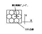
- the incident surface 31 has a first periodic structure 31A that is a group of structures whose refractive index changes in a first period in a two-dimensional direction (XY direction) parallel to the incident surface 31, and the output surface 32 is an output surface.
- 32 has a second periodic structure 32 ⁇ / b> A that is a periodic structure whose refractive index changes in a second period in a two-dimensional direction (XY direction) parallel to 32.
- the first period is shorter than the wavelength of the light generated from the light emitting unit 1, and the second period is longer than the first period.
- the second period may be shorter than the wavelength of the light generated from the light emitting unit 1, may be the same, or may be longer. More preferably, if the wavelength of light generated from the light emitting unit 1 is ⁇ , the first period ⁇ 1 is about ⁇ / 4, and the second period ⁇ 2 is about 5 ⁇ .
- first periodic structure 31 ⁇ / b> A may be formed so as to be in contact with the incident surface 31, or may be formed so as not to be in contact with the incident surface 31.
- the first periodic structure 31 ⁇ / b> A may have a refractive index that changes in a first period in a one-dimensional direction parallel to the incident surface 31.
- the second periodic structure 32 ⁇ / b> A may be formed so as to be in contact with the emission surface 32, or may be formed so as not to be in contact with the emission surface 32.
- the first periodic structure 32 ⁇ / b> A may have a refractive index that changes in a first period in a one-dimensional direction parallel to the emission surface 32.
- the refractive index changes in a one-dimensional direction or a two-dimensional direction parallel to the incident surface 31 at an interval equal to or shorter than the first interval shorter than the wavelength of the light generated from the light emitting unit 1.
- a structure group that does not have a periodic structure may be provided.
- the first periodic structure 31A is a moth-eye structure in which irregularities are formed in a first period in the XY direction
- the second periodic structure 32A is formed in irregularities in a second period in the XY direction. It is assumed that it has a periodic structure like a photonic crystal.
- the convex portion 31B of the first periodic structure 31A and the convex portion 32B of the first periodic structure 32A have a conical shape.
- FIG. 4A is a cross-sectional view in which a part of the first periodic structure 31A is cut by the incident surface 31, and FIG. 4B is a cross-sectional view in which a part of the second periodic structure 32A is cut by the emission surface 32.
- each of the convex portions 31B and 32B is arranged in a triangular lattice shape, and adjacent convex portions are arranged on the incident surface 31 and the outgoing surface 32 without a gap.
- the period of the first periodic structure 31A coincides with the distance from the center of the bottom surface of the convex part 31B to the center of the bottom surface of the adjacent convex part 31B
- the period of the first periodic structure 32A is As shown in FIG. 4B, the distance is the same as the distance from the center of the bottom surface of the convex portion 32B to the center of the bottom surface of the adjacent convex portion 32B.
- Each of the convex portions 31B and 32B may be arranged in another arrangement structure such as a square lattice shape or in another arrangement structure having anisotropy in the XY plane. Further, on the incident surface 31 and the emission surface 32, there may be a gap between adjacent convex portions.
- FIG. 4C is a diagram in which a part of the first periodic structure 31A is cut out along the XY plane between the apex and the bottom of the convex portion 31A.
- the convex portion 31 ⁇ / b> B and the joint portion 2 are arranged in the first cycle in the XY plane. Therefore, since the refractive index of the convex part 31B and the junction part 2 differs from each other, the first periodic structure 31A has a refractive index changing in the first period in the XY plane. That is, by forming the moth-eye structure on the incident surface 31, the refractive index can be changed in the first period with respect to the two-dimensional direction parallel to the incident surface 31. Similarly, by forming the periodic structure on the emission surface 32, the refractive index can be changed in the second period with respect to a two-dimensional direction parallel to the emission surface 32.
- the convex portion 31B has a conical shape
- the volume occupied by the joint portion 2 is larger at the tip of the convex portion 31B than the convex portion 31B, and the bottom surface of the convex portion 31B is larger than the joint portion 2.
- the volume occupied by the convex portion 31B increases.
- the effective refractive index that is an average refractive index in the XY plane of the first periodic structure 31A continuously changes from the tip of the convex portion 31B toward the bottom.
- Fresnel reflection that occurs at the interface between substances having different refractive indexes is less likely to occur as the difference in refractive index between the substances is smaller. Therefore, as described above, the effective refractive index is the tip of the convex portion 31B. Fresnel reflection can be prevented when it continuously changes from the bottom to the bottom.
- the second periodic structure 32A functions as a diffraction grating that diffracts light and guides it in a predetermined direction, the directivity of the light source 10 can be increased.
- the convex portions 31B and 32B are preferably tapered such as a conical shape, but may be other shapes such as a cylindrical shape or a prismatic shape.
- the convex part 31A may have a conical shape and the convex part 32B may have a cylindrical shape.
- the light generated from the light emitting unit 1 is incident on the incident surface 31 of the optical unit 3 through the bonding unit 2.
- the light incident on the incident surface 31 passes through the optical unit 3 with almost no reflection by the first periodic structure 31A. Since the refractive index n1 of the junction part 2 is smaller than the refractive index n2 of the optical part 3, as shown in FIG. 6, when the light passes through the incident surface 31, the exit angle becomes small according to Snell's law, and the exit surface 32 Propagate until.
- the light propagated to the emission surface 32 is emitted after the radiation angle is converted by the second periodic structure 32A.
- the optical unit 3 having the above-described configuration can be manufactured by processing using a glass substrate, PET (Polyethylene terephthalate), an ultraviolet curable resin, or the like as a material by interference exposure, electron beam lithography, nanoimprinting, or the like.
- PET Polyethylene terephthalate
- ultraviolet curable resin or the like as a material by interference exposure, electron beam lithography, nanoimprinting, or the like.
- the fine structure is not processed on both the entrance surface and the exit surface of one optical unit 3, the fine structure is provided on each side of the two optical units 3, and the fine structure of the two optical units 3 is not provided.
- a configuration in which the surfaces are bonded together may be used.
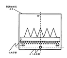
- FIG. 7 is a diagram for explaining a simulation by the FDTD method (Finite Difference Time Domain method) for evaluating the directivity of the light source 10. Moreover, since the difference of the size of each structure is large and it is difficult to represent each structure by an exact ratio, it has shown typically. As shown in FIG. 7, the present simulation performs far field (Far field) by Fourier transforming the intensity distribution of the TE polarized light and TM polarized light emitted concentrically from the point light source 41 and reaching the calculation region end 42. The average of the TE-polarized component and the TM-polarized component in the angular distribution of the light intensity is evaluated. The point light source 41 emits light having a wavelength of 532 nm.
- FDTD method Finite Difference Time Domain method
- the diameter of the bottom surface of the convex portion 31B is fixed to 0.1 ⁇ m, and the height of the convex portion 31B is fixed to 0.5 ⁇ m.
- the light intensity of light was calculated while changing the diameter v of the bottom surface of the convex portion 32B, assuming that the diameter of the bottom surface of the convex portion 32B was v [ ⁇ m], the height of the convex portion 32B was 5 v, and the diameter v of the bottom surface of the convex portion 32B was changed.
- the horizontal axis represents the radiation angle in the far field, and the vertical axis represents the light intensity in the far field that has not been normalized.
- the dotted line indicates the light intensity in the far field when TE polarized light is emitted from the light source, and the straight line indicates the light intensity in the far field when TM polarized light is emitted from the light source.
- there is no optical unit 3 in the calculation area that is, the far-field light intensity of TE polarized light in the case of free space is indicated by a chain line.
- the result of TM polarization is the same as the result of TE polarization, and is omitted.
- the far-field light intensity corresponding to the radiation angle is modulated by diffraction due to the periodic structure of the exit surface of the optical unit 3.
- the ratio of the average value is calculated, it is 1.16, and the directivity is improved.
- FIG. 9 is a diagram showing the relationship between the diameter v of the bottom surface of the convex portion 32B and the gain of light intensity at the calculation region end 42 (Gain of Far field intensity).
- the gain of light intensity is the ratio of the light intensity of the far field at the calculation region end 42 when the optical unit 3 is present to the light intensity of the far field at the calculation region end 42 when the optical unit 3 is not present. It is. Further, FIG.
- the radiation angle is within 15 degrees ( ⁇ 15 degrees to 15 degrees), within 30 degrees ( ⁇ 30 degrees to 30 degrees), within 45 degrees ( ⁇ 45 degrees to 45 degrees), within 60 degrees ( ⁇ 60 degrees to 60 degrees), within 75 degrees (-75 degrees to 75 degrees), within 90 degrees (-90 degrees to 90 degrees), and within 180 degrees (-180 degrees to 180 degrees). Show.
- the light intensity in the radiation angle within 15 degrees to 75 degrees is greater than about 1, and the light source 10 It can be seen that the directivity of is high. Therefore, since the refractive index period in the first periodic structure 31A and the second periodic structure 32A is the distance from the center of the bottom surface of the convex portion to the center of the bottom surface of the adjacent convex portion, the refractive index in the second periodic structure 32A. It can be seen that the directivity of the light source 10 is increased if the second period, which is the period of, is longer than the period of the refractive index in the first periodic structure 31A.
- the aspect ratio (ratio of bottom surface diameter to height) of the convex portions 31B and 32B was calculated as 5. As the aspect ratio is higher, the effect of reducing the Fresnel reflection of the moth-eye structure and the diffraction effect of the photonic crystal are increased, and the light intensity in the far field of FIG. 8 and the gain of the light intensity of FIG. Since the difficulty level increases, it is necessary to determine the aspect ratio by a trade-off between the two. For example, the aspect ratio may be reduced in order to reduce the manufacturing difficulty level.
- FIG. 10 is a layout diagram illustrating an example of the configuration of the projector according to the present embodiment.
- a projector 100 includes light sources 101R, 101G, and 101B, optical elements 102R, 102G, and 102B, liquid crystal panels 103R, 103G, and 103B, a cross dichroic prism 104, and a projection optical system 105.
- Each of the light sources 101R, 101G, and 101B has the same structure as the light source 10 shown in FIG.
- the light emitting units 1 of the light sources 101R, 101G, and 101B generate light having different wavelengths.
- red (R) light is emitted from the light source 101R
- green (G) light is emitted from the light source 101G
- blue (B) light is emitted from the light source 101B.
- Each of the optical elements 102R, 102G, and 102B guides the respective color lights generated from the light sources 101R, 101G, and 101B to the liquid crystal panels 103R, 103G, and 103B, respectively, and enters them.
- the liquid crystal panels 103R, 103G, and 103B are spatial light modulation elements that modulate and emit incident color light according to a video signal.
- the cross dichroic prism 104 combines and outputs the modulated lights emitted from the liquid crystal panels 103R, 103G, and 103B.
- the projection optical system 105 projects the combined light emitted from the cross dichroic prism 104 onto the screen 200 and displays an image corresponding to the video signal on the screen 200.
- FIG. 11 is a layout diagram showing another example of the configuration of the projector according to the present embodiment.
- the projector 100 ′ includes light sources 101 ⁇ / b> R, 101 ⁇ / b> G, and 101 ⁇ / b> B, a light guide 106, a liquid crystal panel 107, and a projection optical system 108.
- the light guide 106 combines the color lights generated from the light sources 101R, 101G, and 101B and outputs the combined light to the liquid crystal panel 107.
- the liquid crystal panel 107 is a spatial light modulation element that modulates incident combined light according to a video signal and emits the modulated light.
- the projection optical system 108 projects the modulated light emitted from the liquid crystal panel 107 onto the screen 200 and displays an image corresponding to the video signal on the screen 200.
- a liquid crystal panel is used as the spatial light modulation element.
- the modulation element is not limited to the liquid crystal panel and can be changed as appropriate.
- a DMD Digital Micromirror Device
- the liquid crystal panel 107 may be used instead of the liquid crystal panel 107.
- the optical unit 3 includes the incident surface 31 on which the light generated from the light emitting unit 1 is incident, and the emission surface 32 that emits the light incident on the incident surface 31.
- the incident surface 31 is formed with a first periodic structure 31 ⁇ / b> A whose refractive index changes in a first period shorter than the wavelength of light in a two-dimensional direction parallel to the incident surface 31.
- a second periodic structure 32 ⁇ / b> A whose refractive index changes in a second period longer than the first period is formed on the emission surface 32 in a two-dimensional direction parallel to the emission surface 32.
- Fresnel reflection occurring on the incident surface 31 can be prevented by the first periodic structure 31A, and the radiation angle of the light emitted from the emission surface 32 can be converted by the second periodic structure 32A. It is possible to increase the light extraction efficiency while increasing.
- the convex portions 31B and 32B are conical, the effective refractive index can be continuously changed in the Z direction perpendicular to the incident surface 31 and the outgoing surface 32, and Fresnel reflection can be performed.
- the prevention effect can be increased.
- FIG. 12 is a perspective view showing the light source of the present embodiment
- FIG. 13 is a longitudinal sectional view of the light source of the present embodiment cut along an XZ plane.
- the 12 and 13 is different from the light source 10 shown in FIG. 1 in that the wall surfaces of the joint portion 2 and the optical portion 3 are formed of a reflecting member 51 that reflects light.
- the junction part 2 is hollow and is filled with air.
- the light incident on the wall surface of the optical unit 3 out of the light generated from the light emitting unit 1 is also reflected by the reflecting member 51 and is incident on the optical unit 3. Since a large amount of light can be guided to the optical unit 3, the light extraction efficiency can be further increased. Further, among the light propagating in the optical unit 3, the light incident on the wall surface of the optical unit 3 can be reflected by the reflecting member 51 and guided to the emission surface 32, so that the light extraction efficiency is further improved. It becomes possible to make it higher.
- all of the wall surfaces of the joint portion 2 and the optical portion 3 are formed of the reflecting member 51. However, only a part of the wall surfaces of the joint portion 2 and the optical portion 3 reflects light. If it is the structure provided with, compared with 1st Embodiment, the extraction efficiency of light can be made high.
- a reflective film that reflects light may be provided on the lower surface or the upper surface of the light emitting unit 1.
Landscapes
- Physics & Mathematics (AREA)
- Engineering & Computer Science (AREA)
- General Physics & Mathematics (AREA)
- Optics & Photonics (AREA)
- Chemical & Material Sciences (AREA)
- Signal Processing (AREA)
- Multimedia (AREA)
- Nanotechnology (AREA)
- Microelectronics & Electronic Packaging (AREA)
- Life Sciences & Earth Sciences (AREA)
- Biophysics (AREA)
- Crystallography & Structural Chemistry (AREA)
- Manufacturing & Machinery (AREA)
- Computer Hardware Design (AREA)
- Power Engineering (AREA)
- Projection Apparatus (AREA)
- Led Device Packages (AREA)
Abstract
指向性を高くしつつ、光の取り出し効率を高くすることが可能な光源を提供する。 光学部(3)は、発光部から発生した光が入射する入射面(31)と、その光を出射する出射面(32)とを有する。入射面(31)上には、屈折率が光の波長より短い第1の間隔以下の間隔で変化する構造物群(31A)が形成されている。出射面32上には、屈折率が第1の間隔より長い第2の間隔で変化する周期構造物(32A)が形成されている。
Description
本発明は、指向性を有する光源に関する。
近年、光源としてLED(Light Emitting Diode)を用いたプロジェクタが注目されている。このようなプロジェクタは、LEDと、LEDからの光が入射される照明光学系と、照明光学系からの光を映像信号に応じて変調して出射する変調素子と、変調素子からの光をスクリーンに投射する投射光学系とを備えている。
上記のプロジェクタでは、投射画像の輝度を高めるために、光源からの光を効率良く投射光として利用することが求められている。光源からの光がどれだけ投射光として利用できるかは、光源の発光面積と放射角との積であるエテンデューによって変化する。より具体的には、光源のエテンデューを、変調素子の受光面積と照明光学系のFナンバーで決まる取り込み角との積の値以下にすると、光源からの光を効率良く投射光として利用することができる。このため、プロジェクタの光源としては、エテンデューを小さくするために、指向性の高い光源が望まれている。
これに対して特許文献1には、所定の方向に効率良く光を出射する発光素子が記載されている。この発光素子では、光を発生する発光部に、発光部からの光を伝播して出射する光学部が積層されている。光学部における光の出射面には、その出射面に平行な2次元方向に対して、屈折率が周期的に変化する周期構造が形成されている。この周期構造によって光が所定の方向に回折されて出射されるので、所定の方向に効率良く光を出射することが可能になる。
特許文献1に記載の発光素子では、光が光学部に入射する際にフレネル反射が発生し、その反射光が発光部に戻ってしまう。発光部に戻された光は、発光素子から出射されない損失となるため、光の取り出し効率が低いという問題がある。なお、発光部に反射膜を設けて、発光部に戻った光を光学部に再入射させることで、光の損失を少なくすることはできる。しかしながら、反射時に光が減衰するため、光の取り出し効率は十分ではない。
本発明の目的は、指向性を高くしつつ、光の取り出し効率を高くすることが可能な光源およびそれを用いた投射型表示装置を提供することである。
本発明による光源は、光を発生する発光部と、前記発光部から発生した光が入射する入射面と、当該光を出射する出射面とを有する光学部とを備え、前記入射面上には、屈折率が前記光の波長より短い第1の間隔以下の間隔で変化する構造物群が形成され、前記出射面上には、屈折率が前記第1の間隔より長い第2の間隔で変化する周期構造物が形成されている。
また、本発明による投射型表示装置は、上記の光源を用いる。
本発明によれば、指向性を高くしつつ、光の取り出し効率を高くすることが可能になる。
以下、本発明の実施形態について図面を参照して説明する。なお、以下の説明では、同じ機能を有するものには同じ符号を付け、その説明を省略する場合がある。
図1は、本発明の第1の実施形態の光源を示す斜視図である。図1に示すように、光源10は、発光部1、接合部2、光学部3の順番に積層されている。
なお、実際の光源における各層の厚さは非常に薄く、また、各層の厚さの違いが大きいので、各層を正確な比率で図示することが困難である。このため、図1では、各層は実際の比率通りには描かれておらず、模式的に示している。また、図1に示すように、発光部1の下面に平行な面をXY平面とし、XY平面と直交する方向をZ方向とする。
発光部1は、光を発生する。より具体的には、発光部1は、p型半導体で形成されたp型層11、活性層12、n型半導体で形成されたn型層13の順番に積層され、p型層11とn型層13との間に外部電源(不図示)によって電圧が印加され、それらの間に電流が流れると、活性層12で光が発生する。
接合部2は、透明誘電体などで形成され、発光部1から発生した光を内部で伝播させて光学部3まで導く。接合部2の屈折率は、光学部3の屈折率より小さいものとする。なお、光源10は、接合部2を設ける代わりに、発光部1および光学部3の間に間隙を設けたものでもよい。
図2は、光学部3を示す斜視図であり、図3は、光学部3をXZ平面で切った縦断面図である。
図2および図3に示すように、光学部3は、発光部1から発生した光が入射する入射面31と、入射面31に入射した光を出射する出射面32とを有する。
入射面31は、入射面31と平行な2次元方向(XY方向)において、屈折率が第1周期で変化する構造物群である第1周期構造31Aを有し、出射面32は、出射面32と平行な2次元方向(XY方向)において、屈折率が第2周期で変化する周期構造物である第2周期構造32Aを有する。第1周期は、発光部1から発生する光の波長より短く、第2周期は、第1周期よりも長い。第2周期は、発光部1から発生する光の波長より短くてもよいし、同じでもよいし、長くてもよい。より好ましくは、発光部1から発生する光の波長をλとすると、第1周期Γ1は、λ/4程度であり、第2周期Γ2は、5λ程度である。
なお、第1周期構造31Aは、入射面31に接するように形成されてもよいし、入射面31に接しないように形成されてもよい。また、第一周期構造31Aは、屈折率が入射面31と平行な一次元方向に第一周期で変化するものでもよい。
また、第2周期構造32Aは、出射面32に接するように形成されてもよいし、出射面32に接しないように形成されてもよい。また、第一周期構造32Aは、屈折率が出射面32と平行な一次元方向に第一周期で変化するものでもよい。
また、第1周期構造31Aの代わりに、入射面31と平行な1次元方向または2次元方向に、屈折率が発光部1から発生する光の波長より短い第1の間隔以下の間隔で変化する、周期構造を有していない構造物群が設けられてもよい。
図2および図3では、第1周期構造31Aは、凹凸がXY方向に第1周期で形成されたモスアイ構造であり、第2周期構造32Aは、凹凸がXY方向に第2周期で形成されたフォトニック結晶のような周期構造であるとしている。また、第1周期構造31Aの凸部31Bと、第1周期構造32Aの凸部32Bは、円錐形状であるとする。
図4Aは、第1周期構造31Aの一部を入射面31で切った横断面図であり、図4Bは、第2周期構造32Aの一部を出射面32で切った横断面図である。
図4Aおよび図4Bに示すように、凸部31Bおよび32Bのそれぞれは、三角格子状に配置されており、入射面31および出射面32上では、隣り合う凸部が隙間なく配置されている。ここで、第1周期構造31Aの周期は、図4Aに示すように、凸部31Bの底面の中心から隣の凸部31B底面の中心までの距離と一致し、第1周期構造32A周期は、図4Bで示すように、凸部32Bの底面の中心から隣の凸部32B底面の中心までの距離と一致している。
なお、凸部31Bおよび32Bのそれぞれは、正方格子状などの他の配置構造や、XY平面内で異方性を有する他の配置構造で配置されてもよい。また、入射面31および出射面32上において、隣り合う凸部に隙間があってもよい。
図4Cは、第1周期構造31Aの一部を凸部31Aの頂点から底面の間のXY平面で切り取った図である。図4Cで示されたように、XY平面内において、凸部31Bと接合部2とが第1周期で配置されている。したがって、凸部31Bと接合部2の屈折率は互いに異なるため、第1周期構造31Aは、XY平面内において、屈折率が第1周期で変化していることになる。つまり、入射面31に上記のモスアイ構造を形成することで、入射面31と平行な2次元方向に対して、屈折率を第1周期で変化させることができる。同様に、出射面32に上記の周期構造を形成することで、出射面32と平行な2次元方向に対して、屈折率を第2周期で変化させることができる。
また、凸部31Bは円錐形状であるため、凸部31Bの先端の方では、凸部31Bに比べて接合部2が占める体積が大きく、凸部31Bの底面の方では、接合部2に比べて凸部31Bが占める体積が大きくなる。このため、第1周期構造31AのXY平面内における平均的な屈折率である有効屈折率は、凸部31Bの先端から底面に向かって連続的に変化していることになる。ここで、互いに異なる屈折率を有する物質間の界面で発生するフレネル反射は、その物質間の屈折率の差が小さいほど発生しづらくなるので、上記のように有効屈折率が凸部31Bの先端から底面に向かって連続的に変化していると、フレネル反射を防止することができる。
また、第2周期構造32Aは光を回折して所定の方向に導く回折格子として機能するので、光源10の指向性を高くすることができる。
なお、凸部31Bおよび32Bは、円錐形状などのテーパー形状が望ましいが、円柱形状や角柱形状などの他の形状でもよい。例えば、光学部3は、図5に示すように、凸部31Aが円錐形状であり、凸部32Bが円柱形状でもよい。
上記の構成を有する光学部3では、発光部1から発生した光は、接合部2を介して光学部3の入射面31に入射する。入射面31に入射した光は、第1周期構造31Aによってほとんど反射することなく、光学部3を透過する。接合部2の屈折率n1が光学部3の屈折率n2より小さいので、図6に示すように、光は、入射面31を透過した際にスネルの法則に従って出射角が小さくなり、出射面32まで伝播する。そして、出射面32に伝播された光は、第2周期構造32Aによって放射角が変換されて出射される。
上記の構成を有する光学部3は、ガラス基板、PET(Polyethylene terephthalate)および紫外線硬化樹脂などを材料に用いて、干渉露光法、電子線リソグラフィーまたはナノインプリントなどによって加工することで作製することが出来る。
また、1つの光学部3の入射面および出射面の両面に微細構造を加工せず、2つの光学部3のそれぞれの片面に微細構造を設け、2つの光学部3の微細構造を設けていない面同士で貼り合せた構成にしても良い。
次に光源10の指向性を評価する。
図7は、光源10の指向性を評価するためのFDTD法(Finite Difference Time Domain method)によるシミュレーションを説明するための図である。また、各構造物のサイズの違いが大きく、各構造物を正確な比率で表すことが困難であるため、模式的に示している。図7に示すように、本シミュレーションは、点光源41から同心円状に出射されたTE偏光およびTM偏光の光の計算領域端42に到達した強度分布をフーリエ変換することで、遠方界(Far field)の光強度の角度分布のTE偏光成分およびTM偏光成分の平均を評価したものである。なお、点光源41からは、波長532nmの光が出射されている。
また、凸部31Bの底面の直径を0.1μmに固定し、凸部31Bの高さを0.5μmに固定する。また、凸部32Bの底面の直径をv[μm]とし、その凸部32Bの高さを5vとし、凸部32Bの底面の直径vを変化させながら光の光強度を計算した。
図8は、一例として、v=4[μm]のときの計算結果を示す図である。横軸は遠方界における放射角を示し、縦軸は遠方界における、規格化をしていない光強度を示す。点線は光源からTE偏光を出射した場合の遠方界での光強度を示し、直線は光源からTM偏光を出射した場合の遠方界での光強度を示している。ここで、リファレンスのために、計算領域内に光学部3がない、つまり自由空間の場合でのTE偏光の遠方界の光強度を鎖線で示している。また自由空間においてはTM偏光の結果はTE偏光の結果と等しいので省略する。
図8に示すグラフから光学部3の出射面の周期構造による回折によって、放射角に応じた遠方界の光強度が変調されていることが判る。ここで、例えば、45度内(-45度~+45度)における自由空間の場合でのTE偏光の遠方界の光強度の積分値に対するTE偏光およびTM偏光の遠方界の光強度の積分値の平均値の割合を計算すると、1.16であり、指向性が向上している。
図9は、凸部32Bの底面の直径vと、計算領域端42における光強度のゲイン(Gain of Far field intensity)との関係を示す図である。ここで、光強度のゲインとは、光学部3が存在しないときの計算領域端42における遠方界の光強度に対する、光学部3が存在するときの計算領域端42における遠方界の光強度の割合である。また、図9は、放射角が15度内(-15度~15度)、30度内(-30度~30度)、45度内(-45度~45度)、60度内(-60度~60度)、75度内(-75度~75度)、90度内(-90度~90度)、180度内(-180度~180度)のそれぞれにおける光強度のゲインを示している。
図9に示すように、凸部32Bの底面の直径が凸部31Bの底面の直径より大きい場合、放射角が15度内~75度内における光強度は略1より大きくなっており、光源10の指向性が高くなっていることが分かる。したがって、第1周期構造31Aおよび第2周期構造32Aにおける屈折率の周期は、凸部の底面の中心から隣の凸部の底面の中心までの距離であるので、第2周期構造32Aにおける屈折率の周期である第2周期が、第1周期構造31Aにおける屈折率の周期よりより長ければ、光源10の指向性を高くなることが分かる。
図8および図9においては、凸部31Bおよび32Bのアスペクト比(底面の直径と高さの比)は5として計算した。アスペクト比が高いほど、モスアイ構造のフレネル反射低減効果やフォトニック結晶の回折効果は高くなり、図8の遠方界での光強度および図9の光強度のゲインが上がるものの、同時に構造物の作製の難易度が上がるので、両者のトレードオフでアスペクト比を決定する必要がある。例えば、作製難易度を下げるために、アスペクト比を下げても良い。
次に光源10を用いた投射型表示装置(プロジェクタ)について説明する。
図10は、本実施形態のプロジェクタの構成の一例を示す配置図である。図10において、プロジェクタ100は、光源101R、101Gおよび101Bと、光学素子102R、102Gおよび102Bと、液晶パネル103R、103Gおよび103Bと、クロスダイクロイックプリズム104と、投射光学系105とを備える。
光源101R、101Gおよび101Bのそれぞれは、図1に示した光源10と同じ構造を有する。光源101R、101Gおよび101Bのそれぞれの発光部1は、波長がそれぞれ異なる光を発生するものとする。以下、光源101Rから赤色(R)光が出射され、光源101Gから緑色(G)光が出射され、光源101Bから青色(B)光が出射されるものとする。
光学素子102R、102Gおよび102Bのそれぞれは、光源101R、101Gおよび101Bから発生した各色光を、液晶パネル103R、103Gおよび103Bのそれぞれに導いて入射する。
液晶パネル103R、103Gおよび103Bは、入射された各色光を映像信号に応じて変調して出射する空間光変調素子である。
クロスダイクロイックプリズム104は、液晶パネル103R、103Gおよび103Bのそれぞれから出射された各変調光を合成して出射する。
投射光学系105は、クロスダイクロイックプリズム104から出射された合成光をスクリーン200に投射して、スクリーン200上に映像信号に応じた映像を表示する。
図11は、本実施形態のプロジェクタの構成の別の例を示す配置図である。図11において、プロジェクタ100’は、光源101R、101Gおよび101Bと、導光体106と、液晶パネル107と、投射光学系108とを有する。
導光体106は、光源101R、101Gおよび101Bから発生した各色光を合成して液晶パネル107に出射する。
液晶パネル107は、入射された合成光を映像信号に応じて変調して出射する空間光変調素子である。
投射光学系108は、液晶パネル107から出射された変調光をスクリーン200に投射して、スクリーン200上に映像信号に応じた映像を表示する。
なお、図10および図11では、空間光変調素子として液晶パネルを用いたが、変調素子は液晶パネルに限らず適宜変更可能である。例えば、図11で示したプロジェクタでは、液晶パネル107の代わりに、DMD(Digital Micromirror Device)を用いてもよい。
以上説明したように本実施形態によれば、光学部3は、発光部1から発生した光が入射する入射面31と、入射面31に入射した光を出射する出射面32とを備える。入射面31には、その入射面31と平行な2次元方向に対して、屈折率が光の波長より短い第1周期で変化する第1周期構造31Aが形成されている。出射面32には、その出射面32と平行な2次元方向に対して、屈折率が第1周期より長い第2周期で変化する第2周期構造32Aが形成されている。
このため、第1周期構造31Aによって入射面31で生じるフレネル反射を防止することができ、第2周期構造32Aによって出射面32から出射される光の放射角を変換することができるので、指向性を高くしつつ、光の取り出し効率を高くすることが可能になる。
また、本実施形態では、凸部31Bおよび32Bは円錐状であるので、入射面31および出射面32と垂直なZ方向に有効屈折率を連続的に変化させることが可能になり、フレネル反射の防止効果を高くすることができる。
次に第2の実施形態について説明する。
図12は、本実施形態の光源を示す斜視図であり、図13は、本実施形態の光源をXZ平面で切った縦断面図である。
図12および図13に示す光源10’は、図1で示した光源10と比べて、接合部2および光学部3の壁面が光を反射する反射部材51で形成されている点が異なる。なお、接合部2は、中空になっており、空気で満たされている。
本実施形態では、発光部1から発生した光のうち光学部3の壁面に入射した光も反射部材51によって反射して光学部3に入射されるので、発光部1から出射された光をより多く光学部3に導くことが可能になるため、光の取り出し効率をより高くすることが可能になる。また、光学部3の内部を伝播する光のうち、光学部3の壁面に入射される光も反射部材51によって反射して出射面32に導くことが可能になるため、光の取り出し効率をより高くすることが可能になる。
なお、本実施形態では、接合部2および光学部3の壁面の全てが反射部材51で形成されていたが、接合部2および光学部3の壁面の一部のみでも、光を反射する反射部が備わった構成であれば、第1の実施形態と比べて、光の取り出し効率を高くすることができる。
以上説明した各実施形態において、図示した構成は単なる一例であって、本発明はその構成に限定されるものではない。
例えば、発光部1の下面や上面などに光を反射する反射膜を設けてもよい。
この出願は、2011年3月9日に出願された日本出願特願2011-051386号公報を基礎とする優先権を主張し、その開示の全てをここに取り込む。
Claims (9)
- 光を発生する発光部と、
前記発光部から発生した光が入射する入射面と、当該光を出射する出射面とを有する光学部とを備え、
前記入射面上には、屈折率が前記光の波長より短い第1の間隔以下の間隔で変化する構造物群が形成され、
前記出射面上には、屈折率が前記第1の間隔より長い第2の間隔で変化する周期構造物が形成されている、光源。 - 請求項1に記載の光源において、
前記構造物群は、凹凸が前記第1周期で形成されたモスアイ構造である、光源。 - 請求項2に記載の光源において、
前記構造物群の凸部は、円錐形状である、光源。 - 請求項1ないし3のいずれか1項に記載の光源において、
前記周期構造物は、凹凸が前記第2周期で形成されたモスアイ構造である、光源。 - 請求項4に記載の光源において、
前記周期構造物の凸部は、円錐形状である、光源。 - 請求項1ないし5のいずれか1項に記載の光源において、
前記発光部および前記光学部は、前記光を伝播する接合部を介して積層され、
前記接合部の屈折率は、前記光学部の屈折率より小さい、光源。 - 請求項6に記載の光源において、
前記接合部は、中空である、光源。 - 請求項6または7に記載の光源において、
前記光学部および前記接合部の壁面の少なくとも一部が前記光を反射する反射部を有する、光源。 - 請求項1ないし8のいずれか1項に記載の光源を用いた投射型表示装置。
Priority Applications (1)
| Application Number | Priority Date | Filing Date | Title |
|---|---|---|---|
| JP2013503336A JPWO2012120738A1 (ja) | 2011-03-09 | 2011-12-02 | 光源およびその光源を用いた投射型表示装置 |
Applications Claiming Priority (2)
| Application Number | Priority Date | Filing Date | Title |
|---|---|---|---|
| JP2011-051386 | 2011-03-09 | ||
| JP2011051386 | 2011-03-09 |
Publications (1)
| Publication Number | Publication Date |
|---|---|
| WO2012120738A1 true WO2012120738A1 (ja) | 2012-09-13 |
Family
ID=46797719
Family Applications (1)
| Application Number | Title | Priority Date | Filing Date |
|---|---|---|---|
| PCT/JP2011/077941 WO2012120738A1 (ja) | 2011-03-09 | 2011-12-02 | 光源およびその光源を用いた投射型表示装置 |
Country Status (2)
| Country | Link |
|---|---|
| JP (1) | JPWO2012120738A1 (ja) |
| WO (1) | WO2012120738A1 (ja) |
Cited By (3)
| Publication number | Priority date | Publication date | Assignee | Title |
|---|---|---|---|---|
| JP2016028275A (ja) * | 2014-07-09 | 2016-02-25 | 恵和株式会社 | 光学シート、エッジライト型のバックライトユニット及び光学シートの製造方法 |
| EP3550334A1 (en) * | 2018-04-04 | 2019-10-09 | Samsung Electronics Co., Ltd. | Light source module including transparent member with meta-surface and electronic device comprising the same |
| JP2022069533A (ja) * | 2017-10-17 | 2022-05-11 | ルミレッズ リミテッド ライアビリティ カンパニー | Ledからの発光をコリメートするためのナノ構造化されたメタマテリアルおよびメタサーフェス |
Citations (2)
| Publication number | Priority date | Publication date | Assignee | Title |
|---|---|---|---|---|
| JP2005274934A (ja) * | 2004-03-24 | 2005-10-06 | Seiko Epson Corp | 光源装置及びプロジェクタ |
| JP2010074090A (ja) * | 2008-09-22 | 2010-04-02 | Meijo Univ | 発光素子、発光素子用サファイア基板及び発光素子用サファイア基板の製造方法 |
-
2011
- 2011-12-02 WO PCT/JP2011/077941 patent/WO2012120738A1/ja active Application Filing
- 2011-12-02 JP JP2013503336A patent/JPWO2012120738A1/ja active Pending
Patent Citations (2)
| Publication number | Priority date | Publication date | Assignee | Title |
|---|---|---|---|---|
| JP2005274934A (ja) * | 2004-03-24 | 2005-10-06 | Seiko Epson Corp | 光源装置及びプロジェクタ |
| JP2010074090A (ja) * | 2008-09-22 | 2010-04-02 | Meijo Univ | 発光素子、発光素子用サファイア基板及び発光素子用サファイア基板の製造方法 |
Cited By (6)
| Publication number | Priority date | Publication date | Assignee | Title |
|---|---|---|---|---|
| JP2016028275A (ja) * | 2014-07-09 | 2016-02-25 | 恵和株式会社 | 光学シート、エッジライト型のバックライトユニット及び光学シートの製造方法 |
| JP2022069533A (ja) * | 2017-10-17 | 2022-05-11 | ルミレッズ リミテッド ライアビリティ カンパニー | Ledからの発光をコリメートするためのナノ構造化されたメタマテリアルおよびメタサーフェス |
| JP7148747B2 (ja) | 2017-10-17 | 2022-10-05 | ルミレッズ リミテッド ライアビリティ カンパニー | Ledからの発光をコリメートするためのナノ構造化されたメタマテリアルおよびメタサーフェス |
| US11726308B2 (en) | 2017-10-17 | 2023-08-15 | Lumileds Llc | Nanostructured meta-materials and meta-surfaces to collimate light emissions from LEDs |
| EP3550334A1 (en) * | 2018-04-04 | 2019-10-09 | Samsung Electronics Co., Ltd. | Light source module including transparent member with meta-surface and electronic device comprising the same |
| US10920957B2 (en) | 2018-04-04 | 2021-02-16 | Samsung Electronics Co., Ltd. | Light source module including transparent member with meta-surface and electronic device comprising the same |
Also Published As
| Publication number | Publication date |
|---|---|
| JPWO2012120738A1 (ja) | 2014-07-07 |
Similar Documents
| Publication | Publication Date | Title |
|---|---|---|
| US9010938B2 (en) | Projector with multiple different types of illumination devices | |
| US8870383B2 (en) | Incoherence device and optical apparatus using same | |
| JP2016085430A (ja) | 虚像表示装置 | |
| JP5772090B2 (ja) | プロジェクター | |
| EP2988170A1 (en) | Light-emitting device and projection system | |
| JP6173456B2 (ja) | 照明デバイス | |
| US9429829B2 (en) | Illumination system and projection apparatus | |
| JP5338987B2 (ja) | 光源および投射型表示装置 | |
| WO2011122555A1 (ja) | 光学素子、光源装置、および投射型表示装置 | |
| US20110305000A1 (en) | Display screen with low-index region surrounding phospors | |
| US10830417B2 (en) | Wavelength converter, light source apparatus, and projector | |
| US9880383B2 (en) | Display device | |
| JP4678231B2 (ja) | 均一化光学素子、照明装置及び画像表示装置 | |
| JP2019174572A (ja) | 光源装置及びプロジェクター | |
| WO2012120738A1 (ja) | 光源およびその光源を用いた投射型表示装置 | |
| JP5170221B2 (ja) | 照明装置および画像表示装置 | |
| JP2017146552A (ja) | 照明装置及びプロジェクター | |
| JP2008070769A (ja) | 光源ユニット、照明装置およびプロジェクタ装置 | |
| JPWO2013157211A1 (ja) | 投射装置 | |
| WO2011162321A1 (ja) | 照明装置及びプロジェクタ | |
| JP2013041132A (ja) | 光学素子、照明装置、およびプロジェクター | |
| KR20100081194A (ko) | 조명 유닛 및 이를 구비한 투사영 조명장치 | |
| WO2014013712A1 (ja) | 光学装置およびそれを用いた表示装置 | |
| JP2007317916A (ja) | 光学素子、発光素子及びプロジェクタ | |
| US10921698B2 (en) | Light source device, projector, and phosphor rod |
Legal Events
| Date | Code | Title | Description |
|---|---|---|---|
| 121 | Ep: the epo has been informed by wipo that ep was designated in this application |
Ref document number: 11860321 Country of ref document: EP Kind code of ref document: A1 |
|
| ENP | Entry into the national phase |
Ref document number: 2013503336 Country of ref document: JP Kind code of ref document: A |
|
| NENP | Non-entry into the national phase |
Ref country code: DE |
|
| 122 | Ep: pct application non-entry in european phase |
Ref document number: 11860321 Country of ref document: EP Kind code of ref document: A1 |