WO2012115132A1 - Transfer film - Google Patents
Transfer film Download PDFInfo
- Publication number
- WO2012115132A1 WO2012115132A1 PCT/JP2012/054223 JP2012054223W WO2012115132A1 WO 2012115132 A1 WO2012115132 A1 WO 2012115132A1 JP 2012054223 W JP2012054223 W JP 2012054223W WO 2012115132 A1 WO2012115132 A1 WO 2012115132A1
- Authority
- WO
- WIPO (PCT)
- Prior art keywords
- transfer layer
- transfer
- film
- thickness
- support film
- Prior art date
Links
- 238000012546 transfer Methods 0.000 title claims abstract description 468
- KPUWHANPEXNPJT-UHFFFAOYSA-N disiloxane Chemical class [SiH3]O[SiH3] KPUWHANPEXNPJT-UHFFFAOYSA-N 0.000 claims abstract description 57
- XUIMIQQOPSSXEZ-UHFFFAOYSA-N Silicon Chemical group [Si] XUIMIQQOPSSXEZ-UHFFFAOYSA-N 0.000 claims abstract description 34
- 238000004833 X-ray photoelectron spectroscopy Methods 0.000 claims abstract description 22
- OKTJSMMVPCPJKN-UHFFFAOYSA-N Carbon Chemical compound [C] OKTJSMMVPCPJKN-UHFFFAOYSA-N 0.000 claims abstract description 15
- QVGXLLKOCUKJST-UHFFFAOYSA-N atomic oxygen Chemical compound [O] QVGXLLKOCUKJST-UHFFFAOYSA-N 0.000 claims abstract description 15
- 229910052799 carbon Inorganic materials 0.000 claims abstract description 15
- 229910052760 oxygen Inorganic materials 0.000 claims abstract description 15
- 239000001301 oxygen Substances 0.000 claims abstract description 15
- 238000005259 measurement Methods 0.000 claims description 60
- 229910052710 silicon Inorganic materials 0.000 claims description 20
- 239000000853 adhesive Substances 0.000 claims description 13
- 230000001070 adhesive effect Effects 0.000 claims description 13
- 239000010703 silicon Substances 0.000 claims description 10
- 239000004925 Acrylic resin Substances 0.000 claims description 7
- 229920000178 Acrylic resin Polymers 0.000 claims description 7
- 229920005672 polyolefin resin Polymers 0.000 claims description 6
- 238000004519 manufacturing process Methods 0.000 abstract description 7
- 239000010410 layer Substances 0.000 description 325
- 238000000034 method Methods 0.000 description 38
- -1 silicon alkoxide Chemical class 0.000 description 29
- 238000010438 heat treatment Methods 0.000 description 26
- 239000000523 sample Substances 0.000 description 26
- 239000011248 coating agent Substances 0.000 description 19
- 238000000576 coating method Methods 0.000 description 18
- 238000007373 indentation Methods 0.000 description 17
- 239000011295 pitch Substances 0.000 description 16
- 238000010586 diagram Methods 0.000 description 15
- 239000000463 material Substances 0.000 description 15
- 230000007547 defect Effects 0.000 description 13
- 230000002829 reductive effect Effects 0.000 description 13
- LYCAIKOWRPUZTN-UHFFFAOYSA-N Ethylene glycol Chemical compound OCCO LYCAIKOWRPUZTN-UHFFFAOYSA-N 0.000 description 12
- 238000011156 evaluation Methods 0.000 description 12
- 239000011521 glass Substances 0.000 description 12
- 229920005989 resin Polymers 0.000 description 12
- 239000011347 resin Substances 0.000 description 12
- 239000000758 substrate Substances 0.000 description 11
- 230000000052 comparative effect Effects 0.000 description 10
- 239000007788 liquid Substances 0.000 description 9
- BLRPTPMANUNPDV-UHFFFAOYSA-N Silane Chemical compound [SiH4] BLRPTPMANUNPDV-UHFFFAOYSA-N 0.000 description 8
- 229910000077 silane Inorganic materials 0.000 description 8
- 238000004364 calculation method Methods 0.000 description 7
- 238000012937 correction Methods 0.000 description 7
- 230000001846 repelling effect Effects 0.000 description 7
- XLYOFNOQVPJJNP-UHFFFAOYSA-N water Substances O XLYOFNOQVPJJNP-UHFFFAOYSA-N 0.000 description 7
- ZHNUHDYFZUAESO-UHFFFAOYSA-N Formamide Chemical compound NC=O ZHNUHDYFZUAESO-UHFFFAOYSA-N 0.000 description 6
- 125000000217 alkyl group Chemical group 0.000 description 6
- 229910052782 aluminium Inorganic materials 0.000 description 6
- XAGFODPZIPBFFR-UHFFFAOYSA-N aluminium Chemical compound [Al] XAGFODPZIPBFFR-UHFFFAOYSA-N 0.000 description 6
- 125000003118 aryl group Chemical group 0.000 description 6
- 125000004432 carbon atom Chemical group C* 0.000 description 6
- 229910052739 hydrogen Inorganic materials 0.000 description 6
- 239000001257 hydrogen Substances 0.000 description 6
- 238000000691 measurement method Methods 0.000 description 6
- 150000001282 organosilanes Chemical class 0.000 description 6
- 238000012360 testing method Methods 0.000 description 6
- VYPSYNLAJGMNEJ-UHFFFAOYSA-N Silicium dioxide Chemical group O=[Si]=O VYPSYNLAJGMNEJ-UHFFFAOYSA-N 0.000 description 5
- 239000006185 dispersion Substances 0.000 description 5
- 238000001035 drying Methods 0.000 description 5
- 238000005530 etching Methods 0.000 description 5
- 239000000203 mixture Substances 0.000 description 5
- 229920006267 polyester film Polymers 0.000 description 5
- 239000002904 solvent Substances 0.000 description 5
- JOLQKTGDSGKSKJ-UHFFFAOYSA-N 1-ethoxypropan-2-ol Chemical compound CCOCC(C)O JOLQKTGDSGKSKJ-UHFFFAOYSA-N 0.000 description 4
- RTZKZFJDLAIYFH-UHFFFAOYSA-N Diethyl ether Chemical compound CCOCC RTZKZFJDLAIYFH-UHFFFAOYSA-N 0.000 description 3
- XEKOWRVHYACXOJ-UHFFFAOYSA-N Ethyl acetate Chemical compound CCOC(C)=O XEKOWRVHYACXOJ-UHFFFAOYSA-N 0.000 description 3
- ZMXDDKWLCZADIW-UHFFFAOYSA-N N,N-Dimethylformamide Chemical compound CN(C)C=O ZMXDDKWLCZADIW-UHFFFAOYSA-N 0.000 description 3
- DNIAPMSPPWPWGF-UHFFFAOYSA-N Propylene glycol Chemical compound CC(O)CO DNIAPMSPPWPWGF-UHFFFAOYSA-N 0.000 description 3
- YXFVVABEGXRONW-UHFFFAOYSA-N Toluene Chemical compound CC1=CC=CC=C1 YXFVVABEGXRONW-UHFFFAOYSA-N 0.000 description 3
- 125000002252 acyl group Chemical group 0.000 description 3
- 239000003513 alkali Substances 0.000 description 3
- 125000003342 alkenyl group Chemical group 0.000 description 3
- 238000005520 cutting process Methods 0.000 description 3
- 125000004122 cyclic group Chemical group 0.000 description 3
- NZZFYRREKKOMAT-UHFFFAOYSA-N diiodomethane Chemical compound ICI NZZFYRREKKOMAT-UHFFFAOYSA-N 0.000 description 3
- 125000001495 ethyl group Chemical group [H]C([H])([H])C([H])([H])* 0.000 description 3
- 230000001788 irregular Effects 0.000 description 3
- 239000002346 layers by function Substances 0.000 description 3
- VLKZOEOYAKHREP-UHFFFAOYSA-N n-Hexane Chemical compound CCCCCC VLKZOEOYAKHREP-UHFFFAOYSA-N 0.000 description 3
- 238000002360 preparation method Methods 0.000 description 3
- LLHKCFNBLRBOGN-UHFFFAOYSA-N propylene glycol methyl ether acetate Chemical compound COCC(C)OC(C)=O LLHKCFNBLRBOGN-UHFFFAOYSA-N 0.000 description 3
- 150000004756 silanes Chemical class 0.000 description 3
- 239000000126 substance Substances 0.000 description 3
- LFQCEHFDDXELDD-UHFFFAOYSA-N tetramethyl orthosilicate Chemical compound CO[Si](OC)(OC)OC LFQCEHFDDXELDD-UHFFFAOYSA-N 0.000 description 3
- DURPTKYDGMDSBL-UHFFFAOYSA-N 1-butoxybutane Chemical compound CCCCOCCCC DURPTKYDGMDSBL-UHFFFAOYSA-N 0.000 description 2
- RRQYJINTUHWNHW-UHFFFAOYSA-N 1-ethoxy-2-(2-ethoxyethoxy)ethane Chemical compound CCOCCOCCOCC RRQYJINTUHWNHW-UHFFFAOYSA-N 0.000 description 2
- ARXJGSRGQADJSQ-UHFFFAOYSA-N 1-methoxypropan-2-ol Chemical compound COCC(C)O ARXJGSRGQADJSQ-UHFFFAOYSA-N 0.000 description 2
- HXVNBWAKAOHACI-UHFFFAOYSA-N 2,4-dimethyl-3-pentanone Chemical compound CC(C)C(=O)C(C)C HXVNBWAKAOHACI-UHFFFAOYSA-N 0.000 description 2
- PTTPXKJBFFKCEK-UHFFFAOYSA-N 2-Methyl-4-heptanone Chemical compound CC(C)CC(=O)CC(C)C PTTPXKJBFFKCEK-UHFFFAOYSA-N 0.000 description 2
- SZNYYWIUQFZLLT-UHFFFAOYSA-N 2-methyl-1-(2-methylpropoxy)propane Chemical compound CC(C)COCC(C)C SZNYYWIUQFZLLT-UHFFFAOYSA-N 0.000 description 2
- VATRWWPJWVCZTA-UHFFFAOYSA-N 3-oxo-n-[2-(trifluoromethyl)phenyl]butanamide Chemical compound CC(=O)CC(=O)NC1=CC=CC=C1C(F)(F)F VATRWWPJWVCZTA-UHFFFAOYSA-N 0.000 description 2
- YEJRWHAVMIAJKC-UHFFFAOYSA-N 4-Butyrolactone Chemical compound O=C1CCCO1 YEJRWHAVMIAJKC-UHFFFAOYSA-N 0.000 description 2
- DKPFZGUDAPQIHT-UHFFFAOYSA-N Butyl acetate Natural products CCCCOC(C)=O DKPFZGUDAPQIHT-UHFFFAOYSA-N 0.000 description 2
- IAZDPXIOMUYVGZ-UHFFFAOYSA-N Dimethylsulphoxide Chemical compound CS(C)=O IAZDPXIOMUYVGZ-UHFFFAOYSA-N 0.000 description 2
- YCKRFDGAMUMZLT-UHFFFAOYSA-N Fluorine atom Chemical compound [F] YCKRFDGAMUMZLT-UHFFFAOYSA-N 0.000 description 2
- NTIZESTWPVYFNL-UHFFFAOYSA-N Methyl isobutyl ketone Chemical compound CC(C)CC(C)=O NTIZESTWPVYFNL-UHFFFAOYSA-N 0.000 description 2
- UIHCLUNTQKBZGK-UHFFFAOYSA-N Methyl isobutyl ketone Natural products CCC(C)C(C)=O UIHCLUNTQKBZGK-UHFFFAOYSA-N 0.000 description 2
- SECXISVLQFMRJM-UHFFFAOYSA-N N-Methylpyrrolidone Chemical compound CN1CCCC1=O SECXISVLQFMRJM-UHFFFAOYSA-N 0.000 description 2
- 239000004721 Polyphenylene oxide Substances 0.000 description 2
- 239000004793 Polystyrene Substances 0.000 description 2
- 230000015572 biosynthetic process Effects 0.000 description 2
- 230000008859 change Effects 0.000 description 2
- 239000003795 chemical substances by application Substances 0.000 description 2
- 238000004140 cleaning Methods 0.000 description 2
- 238000009833 condensation Methods 0.000 description 2
- 230000005494 condensation Effects 0.000 description 2
- 238000012790 confirmation Methods 0.000 description 2
- 239000013078 crystal Substances 0.000 description 2
- 238000001723 curing Methods 0.000 description 2
- JHIVVAPYMSGYDF-UHFFFAOYSA-N cyclohexanone Chemical compound O=C1CCCCC1 JHIVVAPYMSGYDF-UHFFFAOYSA-N 0.000 description 2
- BGTOWKSIORTVQH-UHFFFAOYSA-N cyclopentanone Chemical compound O=C1CCCC1 BGTOWKSIORTVQH-UHFFFAOYSA-N 0.000 description 2
- 238000000354 decomposition reaction Methods 0.000 description 2
- 229910003460 diamond Inorganic materials 0.000 description 2
- 239000010432 diamond Substances 0.000 description 2
- 229940019778 diethylene glycol diethyl ether Drugs 0.000 description 2
- SBZXBUIDTXKZTM-UHFFFAOYSA-N diglyme Chemical compound COCCOCCOC SBZXBUIDTXKZTM-UHFFFAOYSA-N 0.000 description 2
- USIUVYZYUHIAEV-UHFFFAOYSA-N diphenyl ether Chemical compound C=1C=CC=CC=1OC1=CC=CC=C1 USIUVYZYUHIAEV-UHFFFAOYSA-N 0.000 description 2
- 239000000428 dust Substances 0.000 description 2
- 230000000694 effects Effects 0.000 description 2
- XLLIQLLCWZCATF-UHFFFAOYSA-N ethylene glycol monomethyl ether acetate Natural products COCCOC(C)=O XLLIQLLCWZCATF-UHFFFAOYSA-N 0.000 description 2
- 238000002474 experimental method Methods 0.000 description 2
- 239000011737 fluorine Substances 0.000 description 2
- 229910052731 fluorine Inorganic materials 0.000 description 2
- 238000001879 gelation Methods 0.000 description 2
- CATSNJVOTSVZJV-UHFFFAOYSA-N heptan-2-one Chemical compound CCCCCC(C)=O CATSNJVOTSVZJV-UHFFFAOYSA-N 0.000 description 2
- NGAZZOYFWWSOGK-UHFFFAOYSA-N heptan-3-one Chemical compound CCCCC(=O)CC NGAZZOYFWWSOGK-UHFFFAOYSA-N 0.000 description 2
- FUZZWVXGSFPDMH-UHFFFAOYSA-N hexanoic acid Chemical compound CCCCCC(O)=O FUZZWVXGSFPDMH-UHFFFAOYSA-N 0.000 description 2
- 125000004435 hydrogen atom Chemical class [H]* 0.000 description 2
- 230000007062 hydrolysis Effects 0.000 description 2
- 238000006460 hydrolysis reaction Methods 0.000 description 2
- 238000003384 imaging method Methods 0.000 description 2
- 229910010272 inorganic material Inorganic materials 0.000 description 2
- 239000011147 inorganic material Substances 0.000 description 2
- 125000001449 isopropyl group Chemical group [H]C([H])([H])C([H])(*)C([H])([H])[H] 0.000 description 2
- 238000010030 laminating Methods 0.000 description 2
- 238000003475 lamination Methods 0.000 description 2
- 125000002496 methyl group Chemical group [H]C([H])([H])* 0.000 description 2
- 125000004108 n-butyl group Chemical group [H]C([H])([H])C([H])([H])C([H])([H])C([H])([H])* 0.000 description 2
- 125000001280 n-hexyl group Chemical group C(CCCCC)* 0.000 description 2
- 125000004123 n-propyl group Chemical group [H]C([H])([H])C([H])([H])C([H])([H])* 0.000 description 2
- 125000001624 naphthyl group Chemical group 0.000 description 2
- 239000002245 particle Substances 0.000 description 2
- 125000001997 phenyl group Chemical group [H]C1=C([H])C([H])=C(*)C([H])=C1[H] 0.000 description 2
- BASFCYQUMIYNBI-UHFFFAOYSA-N platinum Chemical compound [Pt] BASFCYQUMIYNBI-UHFFFAOYSA-N 0.000 description 2
- 229920000570 polyether Polymers 0.000 description 2
- 238000006116 polymerization reaction Methods 0.000 description 2
- 229920002223 polystyrene Polymers 0.000 description 2
- 238000003825 pressing Methods 0.000 description 2
- 230000008569 process Effects 0.000 description 2
- 238000012545 processing Methods 0.000 description 2
- 239000013074 reference sample Substances 0.000 description 2
- 238000003980 solgel method Methods 0.000 description 2
- 238000004383 yellowing Methods 0.000 description 2
- WYTZZXDRDKSJID-UHFFFAOYSA-N (3-aminopropyl)triethoxysilane Chemical compound CCO[Si](OCC)(OCC)CCCN WYTZZXDRDKSJID-UHFFFAOYSA-N 0.000 description 1
- RYNQKSJRFHJZTK-UHFFFAOYSA-N (3-methoxy-3-methylbutyl) acetate Chemical compound COC(C)(C)CCOC(C)=O RYNQKSJRFHJZTK-UHFFFAOYSA-N 0.000 description 1
- QYGBYAQGBVHMDD-XQRVVYSFSA-N (z)-2-cyano-3-thiophen-2-ylprop-2-enoic acid Chemical compound OC(=O)C(\C#N)=C/C1=CC=CS1 QYGBYAQGBVHMDD-XQRVVYSFSA-N 0.000 description 1
- OKIRBHVFJGXOIS-UHFFFAOYSA-N 1,2-di(propan-2-yl)benzene Chemical compound CC(C)C1=CC=CC=C1C(C)C OKIRBHVFJGXOIS-UHFFFAOYSA-N 0.000 description 1
- WKBPZYKAUNRMKP-UHFFFAOYSA-N 1-[2-(2,4-dichlorophenyl)pentyl]1,2,4-triazole Chemical compound C=1C=C(Cl)C=C(Cl)C=1C(CCC)CN1C=NC=N1 WKBPZYKAUNRMKP-UHFFFAOYSA-N 0.000 description 1
- RWNUSVWFHDHRCJ-UHFFFAOYSA-N 1-butoxypropan-2-ol Chemical compound CCCCOCC(C)O RWNUSVWFHDHRCJ-UHFFFAOYSA-N 0.000 description 1
- XNWFRZJHXBZDAG-UHFFFAOYSA-N 2-METHOXYETHANOL Chemical compound COCCO XNWFRZJHXBZDAG-UHFFFAOYSA-N 0.000 description 1
- SVONRAPFKPVNKG-UHFFFAOYSA-N 2-ethoxyethyl acetate Chemical compound CCOCCOC(C)=O SVONRAPFKPVNKG-UHFFFAOYSA-N 0.000 description 1
- MFKRHJVUCZRDTF-UHFFFAOYSA-N 3-methoxy-3-methylbutan-1-ol Chemical compound COC(C)(C)CCO MFKRHJVUCZRDTF-UHFFFAOYSA-N 0.000 description 1
- LDMRLRNXHLPZJN-UHFFFAOYSA-N 3-propoxypropan-1-ol Chemical compound CCCOCCCO LDMRLRNXHLPZJN-UHFFFAOYSA-N 0.000 description 1
- DCQBZYNUSLHVJC-UHFFFAOYSA-N 3-triethoxysilylpropane-1-thiol Chemical compound CCO[Si](OCC)(OCC)CCCS DCQBZYNUSLHVJC-UHFFFAOYSA-N 0.000 description 1
- URDOJQUSEUXVRP-UHFFFAOYSA-N 3-triethoxysilylpropyl 2-methylprop-2-enoate Chemical compound CCO[Si](OCC)(OCC)CCCOC(=O)C(C)=C URDOJQUSEUXVRP-UHFFFAOYSA-N 0.000 description 1
- SJECZPVISLOESU-UHFFFAOYSA-N 3-trimethoxysilylpropan-1-amine Chemical compound CO[Si](OC)(OC)CCCN SJECZPVISLOESU-UHFFFAOYSA-N 0.000 description 1
- KBQVDAIIQCXKPI-UHFFFAOYSA-N 3-trimethoxysilylpropyl prop-2-enoate Chemical compound CO[Si](OC)(OC)CCCOC(=O)C=C KBQVDAIIQCXKPI-UHFFFAOYSA-N 0.000 description 1
- 101100064324 Arabidopsis thaliana DTX48 gene Proteins 0.000 description 1
- 238000012935 Averaging Methods 0.000 description 1
- XDTMQSROBMDMFD-UHFFFAOYSA-N Cyclohexane Chemical compound C1CCCCC1 XDTMQSROBMDMFD-UHFFFAOYSA-N 0.000 description 1
- ZAFNJMIOTHYJRJ-UHFFFAOYSA-N Diisopropyl ether Chemical compound CC(C)OC(C)C ZAFNJMIOTHYJRJ-UHFFFAOYSA-N 0.000 description 1
- 229920000181 Ethylene propylene rubber Polymers 0.000 description 1
- FXHOOIRPVKKKFG-UHFFFAOYSA-N N,N-Dimethylacetamide Chemical compound CN(C)C(C)=O FXHOOIRPVKKKFG-UHFFFAOYSA-N 0.000 description 1
- 229920000459 Nitrile rubber Polymers 0.000 description 1
- CTQNGGLPUBDAKN-UHFFFAOYSA-N O-Xylene Chemical compound CC1=CC=CC=C1C CTQNGGLPUBDAKN-UHFFFAOYSA-N 0.000 description 1
- 239000004698 Polyethylene Substances 0.000 description 1
- 229920002367 Polyisobutene Polymers 0.000 description 1
- 239000004743 Polypropylene Substances 0.000 description 1
- BOTDANWDWHJENH-UHFFFAOYSA-N Tetraethyl orthosilicate Chemical compound CCO[Si](OCC)(OCC)OCC BOTDANWDWHJENH-UHFFFAOYSA-N 0.000 description 1
- 125000002777 acetyl group Chemical group [H]C([H])([H])C(*)=O 0.000 description 1
- 150000001298 alcohols Chemical class 0.000 description 1
- 150000001338 aliphatic hydrocarbons Chemical class 0.000 description 1
- 150000001408 amides Chemical class 0.000 description 1
- 230000003373 anti-fouling effect Effects 0.000 description 1
- 238000000149 argon plasma sintering Methods 0.000 description 1
- 150000004945 aromatic hydrocarbons Chemical class 0.000 description 1
- 239000012298 atmosphere Substances 0.000 description 1
- 125000004429 atom Chemical group 0.000 description 1
- 230000001588 bifunctional effect Effects 0.000 description 1
- 238000009835 boiling Methods 0.000 description 1
- 229920005549 butyl rubber Polymers 0.000 description 1
- XGZGKDQVCBHSGI-UHFFFAOYSA-N butyl(triethoxy)silane Chemical compound CCCC[Si](OCC)(OCC)OCC XGZGKDQVCBHSGI-UHFFFAOYSA-N 0.000 description 1
- SXPLZNMUBFBFIA-UHFFFAOYSA-N butyl(trimethoxy)silane Chemical compound CCCC[Si](OC)(OC)OC SXPLZNMUBFBFIA-UHFFFAOYSA-N 0.000 description 1
- 238000006243 chemical reaction Methods 0.000 description 1
- 239000008119 colloidal silica Substances 0.000 description 1
- 238000003851 corona treatment Methods 0.000 description 1
- KQAHMVLQCSALSX-UHFFFAOYSA-N decyl(trimethoxy)silane Chemical compound CCCCCCCCCC[Si](OC)(OC)OC KQAHMVLQCSALSX-UHFFFAOYSA-N 0.000 description 1
- 230000018044 dehydration Effects 0.000 description 1
- 238000006297 dehydration reaction Methods 0.000 description 1
- 230000008021 deposition Effects 0.000 description 1
- YPENMAABQGWRBR-UHFFFAOYSA-N dibutyl(dimethoxy)silane Chemical compound CCCC[Si](OC)(OC)CCCC YPENMAABQGWRBR-UHFFFAOYSA-N 0.000 description 1
- 238000007865 diluting Methods 0.000 description 1
- JJQZDUKDJDQPMQ-UHFFFAOYSA-N dimethoxy(dimethyl)silane Chemical compound CO[Si](C)(C)OC JJQZDUKDJDQPMQ-UHFFFAOYSA-N 0.000 description 1
- AHUXYBVKTIBBJW-UHFFFAOYSA-N dimethoxy(diphenyl)silane Chemical compound C=1C=CC=CC=1[Si](OC)(OC)C1=CC=CC=C1 AHUXYBVKTIBBJW-UHFFFAOYSA-N 0.000 description 1
- YYLGKUPAFFKGRQ-UHFFFAOYSA-N dimethyldiethoxysilane Chemical compound CCO[Si](C)(C)OCC YYLGKUPAFFKGRQ-UHFFFAOYSA-N 0.000 description 1
- NYMVBZHJSKIHQK-UHFFFAOYSA-N dimethylsilyl acetate Chemical compound C[SiH](C)OC(C)=O NYMVBZHJSKIHQK-UHFFFAOYSA-N 0.000 description 1
- 238000006073 displacement reaction Methods 0.000 description 1
- 229920001971 elastomer Polymers 0.000 description 1
- 150000002148 esters Chemical class 0.000 description 1
- 150000002168 ethanoic acid esters Chemical class 0.000 description 1
- FWDBOZPQNFPOLF-UHFFFAOYSA-N ethenyl(triethoxy)silane Chemical compound CCO[Si](OCC)(OCC)C=C FWDBOZPQNFPOLF-UHFFFAOYSA-N 0.000 description 1
- NKSJNEHGWDZZQF-UHFFFAOYSA-N ethenyl(trimethoxy)silane Chemical compound CO[Si](OC)(OC)C=C NKSJNEHGWDZZQF-UHFFFAOYSA-N 0.000 description 1
- SBRXLTRZCJVAPH-UHFFFAOYSA-N ethyl(trimethoxy)silane Chemical compound CC[Si](OC)(OC)OC SBRXLTRZCJVAPH-UHFFFAOYSA-N 0.000 description 1
- MYEJNNDSIXAGNK-UHFFFAOYSA-N ethyl-tri(propan-2-yloxy)silane Chemical compound CC(C)O[Si](CC)(OC(C)C)OC(C)C MYEJNNDSIXAGNK-UHFFFAOYSA-N 0.000 description 1
- 238000001125 extrusion Methods 0.000 description 1
- 125000000524 functional group Chemical group 0.000 description 1
- 150000002334 glycols Chemical class 0.000 description 1
- PCHJSUWPFVWCPO-UHFFFAOYSA-N gold Chemical compound [Au] PCHJSUWPFVWCPO-UHFFFAOYSA-N 0.000 description 1
- 229910052737 gold Inorganic materials 0.000 description 1
- 239000010931 gold Substances 0.000 description 1
- 125000003104 hexanoyl group Chemical group O=C([*])C([H])([H])C([H])([H])C([H])([H])C([H])([H])C([H])([H])[H] 0.000 description 1
- CZWLNMOIEMTDJY-UHFFFAOYSA-N hexyl(trimethoxy)silane Chemical compound CCCCCC[Si](OC)(OC)OC CZWLNMOIEMTDJY-UHFFFAOYSA-N 0.000 description 1
- 238000005984 hydrogenation reaction Methods 0.000 description 1
- 150000002576 ketones Chemical class 0.000 description 1
- 239000004973 liquid crystal related substance Substances 0.000 description 1
- AUHZEENZYGFFBQ-UHFFFAOYSA-N mesitylene Substances CC1=CC(C)=CC(C)=C1 AUHZEENZYGFFBQ-UHFFFAOYSA-N 0.000 description 1
- 125000001827 mesitylenyl group Chemical group [H]C1=C(C(*)=C(C([H])=C1C([H])([H])[H])C([H])([H])[H])C([H])([H])[H] 0.000 description 1
- 229910052751 metal Inorganic materials 0.000 description 1
- 239000002184 metal Substances 0.000 description 1
- POPACFLNWGUDSR-UHFFFAOYSA-N methoxy(trimethyl)silane Chemical compound CO[Si](C)(C)C POPACFLNWGUDSR-UHFFFAOYSA-N 0.000 description 1
- HLXDKGBELJJMHR-UHFFFAOYSA-N methyl-tri(propan-2-yloxy)silane Chemical compound CC(C)O[Si](C)(OC(C)C)OC(C)C HLXDKGBELJJMHR-UHFFFAOYSA-N 0.000 description 1
- BFXIKLCIZHOAAZ-UHFFFAOYSA-N methyltrimethoxysilane Chemical compound CO[Si](C)(OC)OC BFXIKLCIZHOAAZ-UHFFFAOYSA-N 0.000 description 1
- 239000006082 mold release agent Substances 0.000 description 1
- 239000000178 monomer Substances 0.000 description 1
- 125000000740 n-pentyl group Chemical group [H]C([H])([H])C([H])([H])C([H])([H])C([H])([H])C([H])([H])* 0.000 description 1
- 229910000510 noble metal Inorganic materials 0.000 description 1
- 230000003287 optical effect Effects 0.000 description 1
- 239000003960 organic solvent Substances 0.000 description 1
- 230000036961 partial effect Effects 0.000 description 1
- 238000000016 photochemical curing Methods 0.000 description 1
- 229910052697 platinum Inorganic materials 0.000 description 1
- 229920006122 polyamide resin Polymers 0.000 description 1
- 229920001083 polybutene Polymers 0.000 description 1
- 229920001707 polybutylene terephthalate Polymers 0.000 description 1
- 239000004431 polycarbonate resin Substances 0.000 description 1
- 229920005668 polycarbonate resin Polymers 0.000 description 1
- 238000006068 polycondensation reaction Methods 0.000 description 1
- 229920001225 polyester resin Polymers 0.000 description 1
- 239000004645 polyester resin Substances 0.000 description 1
- 229920006149 polyester-amide block copolymer Polymers 0.000 description 1
- 229920000573 polyethylene Polymers 0.000 description 1
- 229920000139 polyethylene terephthalate Polymers 0.000 description 1
- 239000005020 polyethylene terephthalate Substances 0.000 description 1
- 229920001721 polyimide Polymers 0.000 description 1
- 239000009719 polyimide resin Substances 0.000 description 1
- 230000000379 polymerizing effect Effects 0.000 description 1
- 229920000306 polymethylpentene Polymers 0.000 description 1
- 239000011116 polymethylpentene Substances 0.000 description 1
- 229920001155 polypropylene Polymers 0.000 description 1
- 229920001296 polysiloxane Polymers 0.000 description 1
- 229920000734 polysilsesquioxane polymer Polymers 0.000 description 1
- 229920005749 polyurethane resin Polymers 0.000 description 1
- 229920000915 polyvinyl chloride Polymers 0.000 description 1
- 239000004800 polyvinyl chloride Substances 0.000 description 1
- 238000012805 post-processing Methods 0.000 description 1
- 238000010248 power generation Methods 0.000 description 1
- 230000002265 prevention Effects 0.000 description 1
- 230000001681 protective effect Effects 0.000 description 1
- 239000002994 raw material Substances 0.000 description 1
- 230000009467 reduction Effects 0.000 description 1
- 230000004044 response Effects 0.000 description 1
- 230000002441 reversible effect Effects 0.000 description 1
- 239000005060 rubber Substances 0.000 description 1
- 239000004065 semiconductor Substances 0.000 description 1
- 230000035945 sensitivity Effects 0.000 description 1
- 239000000377 silicon dioxide Substances 0.000 description 1
- 235000012239 silicon dioxide Nutrition 0.000 description 1
- 229920002050 silicone resin Polymers 0.000 description 1
- 229920002379 silicone rubber Polymers 0.000 description 1
- 230000003068 static effect Effects 0.000 description 1
- 238000003860 storage Methods 0.000 description 1
- 239000013077 target material Substances 0.000 description 1
- 229910052714 tellurium Inorganic materials 0.000 description 1
- PORWMNRCUJJQNO-UHFFFAOYSA-N tellurium atom Chemical compound [Te] PORWMNRCUJJQNO-UHFFFAOYSA-N 0.000 description 1
- 238000009864 tensile test Methods 0.000 description 1
- 125000000999 tert-butyl group Chemical group [H]C([H])([H])C(*)(C([H])([H])[H])C([H])([H])[H] 0.000 description 1
- ADLSSRLDGACTEX-UHFFFAOYSA-N tetraphenyl silicate Chemical compound C=1C=CC=CC=1O[Si](OC=1C=CC=CC=1)(OC=1C=CC=CC=1)OC1=CC=CC=C1 ADLSSRLDGACTEX-UHFFFAOYSA-N 0.000 description 1
- 125000003944 tolyl group Chemical group 0.000 description 1
- YZVRVDPMGYFCGL-UHFFFAOYSA-N triacetyloxysilyl acetate Chemical compound CC(=O)O[Si](OC(C)=O)(OC(C)=O)OC(C)=O YZVRVDPMGYFCGL-UHFFFAOYSA-N 0.000 description 1
- GIHPVQDFBJMUAO-UHFFFAOYSA-N tributoxy(ethyl)silane Chemical compound CCCCO[Si](CC)(OCCCC)OCCCC GIHPVQDFBJMUAO-UHFFFAOYSA-N 0.000 description 1
- GYZQBXUDWTVJDF-UHFFFAOYSA-N tributoxy(methyl)silane Chemical compound CCCCO[Si](C)(OCCCC)OCCCC GYZQBXUDWTVJDF-UHFFFAOYSA-N 0.000 description 1
- ISEIIPDWJVGTQS-UHFFFAOYSA-N tributylsilicon Chemical compound CCCC[Si](CCCC)CCCC ISEIIPDWJVGTQS-UHFFFAOYSA-N 0.000 description 1
- DENFJSAFJTVPJR-UHFFFAOYSA-N triethoxy(ethyl)silane Chemical compound CCO[Si](CC)(OCC)OCC DENFJSAFJTVPJR-UHFFFAOYSA-N 0.000 description 1
- WUMSTCDLAYQDNO-UHFFFAOYSA-N triethoxy(hexyl)silane Chemical compound CCCCCC[Si](OCC)(OCC)OCC WUMSTCDLAYQDNO-UHFFFAOYSA-N 0.000 description 1
- CPUDPFPXCZDNGI-UHFFFAOYSA-N triethoxy(methyl)silane Chemical compound CCO[Si](C)(OCC)OCC CPUDPFPXCZDNGI-UHFFFAOYSA-N 0.000 description 1
- JCVQKRGIASEUKR-UHFFFAOYSA-N triethoxy(phenyl)silane Chemical compound CCO[Si](OCC)(OCC)C1=CC=CC=C1 JCVQKRGIASEUKR-UHFFFAOYSA-N 0.000 description 1
- NBXZNTLFQLUFES-UHFFFAOYSA-N triethoxy(propyl)silane Chemical compound CCC[Si](OCC)(OCC)OCC NBXZNTLFQLUFES-UHFFFAOYSA-N 0.000 description 1
- BOVWGKNFLVZRDU-UHFFFAOYSA-N triethoxy(trifluoromethyl)silane Chemical compound CCO[Si](OCC)(OCC)C(F)(F)F BOVWGKNFLVZRDU-UHFFFAOYSA-N 0.000 description 1
- JXUKBNICSRJFAP-UHFFFAOYSA-N triethoxy-[3-(oxiran-2-ylmethoxy)propyl]silane Chemical compound CCO[Si](OCC)(OCC)CCCOCC1CO1 JXUKBNICSRJFAP-UHFFFAOYSA-N 0.000 description 1
- 125000002023 trifluoromethyl group Chemical group FC(F)(F)* 0.000 description 1
- JLGNHOJUQFHYEZ-UHFFFAOYSA-N trimethoxy(3,3,3-trifluoropropyl)silane Chemical compound CO[Si](OC)(OC)CCC(F)(F)F JLGNHOJUQFHYEZ-UHFFFAOYSA-N 0.000 description 1
- ZNOCGWVLWPVKAO-UHFFFAOYSA-N trimethoxy(phenyl)silane Chemical compound CO[Si](OC)(OC)C1=CC=CC=C1 ZNOCGWVLWPVKAO-UHFFFAOYSA-N 0.000 description 1
- HQYALQRYBUJWDH-UHFFFAOYSA-N trimethoxy(propyl)silane Chemical compound CCC[Si](OC)(OC)OC HQYALQRYBUJWDH-UHFFFAOYSA-N 0.000 description 1
- ORVBHOQTQDOUIW-UHFFFAOYSA-N trimethoxy(trifluoromethyl)silane Chemical compound CO[Si](OC)(OC)C(F)(F)F ORVBHOQTQDOUIW-UHFFFAOYSA-N 0.000 description 1
- DQZNLOXENNXVAD-UHFFFAOYSA-N trimethoxy-[2-(7-oxabicyclo[4.1.0]heptan-4-yl)ethyl]silane Chemical compound C1C(CC[Si](OC)(OC)OC)CCC2OC21 DQZNLOXENNXVAD-UHFFFAOYSA-N 0.000 description 1
- BPSIOYPQMFLKFR-UHFFFAOYSA-N trimethoxy-[3-(oxiran-2-ylmethoxy)propyl]silane Chemical compound CO[Si](OC)(OC)CCCOCC1CO1 BPSIOYPQMFLKFR-UHFFFAOYSA-N 0.000 description 1
- 125000003774 valeryl group Chemical group O=C([*])C([H])([H])C([H])([H])C([H])([H])C([H])([H])[H] 0.000 description 1
- 125000000391 vinyl group Chemical group [H]C([*])=C([H])[H] 0.000 description 1
- 238000005406 washing Methods 0.000 description 1
- 239000008096 xylene Substances 0.000 description 1
Images


Classifications
-
- B—PERFORMING OPERATIONS; TRANSPORTING
- B32—LAYERED PRODUCTS
- B32B—LAYERED PRODUCTS, i.e. PRODUCTS BUILT-UP OF STRATA OF FLAT OR NON-FLAT, e.g. CELLULAR OR HONEYCOMB, FORM
- B32B27/00—Layered products comprising a layer of synthetic resin
- B32B27/06—Layered products comprising a layer of synthetic resin as the main or only constituent of a layer, which is next to another layer of the same or of a different material
- B32B27/08—Layered products comprising a layer of synthetic resin as the main or only constituent of a layer, which is next to another layer of the same or of a different material of synthetic resin
-
- B—PERFORMING OPERATIONS; TRANSPORTING
- B44—DECORATIVE ARTS
- B44C—PRODUCING DECORATIVE EFFECTS; MOSAICS; TARSIA WORK; PAPERHANGING
- B44C1/00—Processes, not specifically provided for elsewhere, for producing decorative surface effects
- B44C1/16—Processes, not specifically provided for elsewhere, for producing decorative surface effects for applying transfer pictures or the like
- B44C1/165—Processes, not specifically provided for elsewhere, for producing decorative surface effects for applying transfer pictures or the like for decalcomanias; sheet material therefor
- B44C1/17—Dry transfer
-
- B—PERFORMING OPERATIONS; TRANSPORTING
- B29—WORKING OF PLASTICS; WORKING OF SUBSTANCES IN A PLASTIC STATE IN GENERAL
- B29C—SHAPING OR JOINING OF PLASTICS; SHAPING OF MATERIAL IN A PLASTIC STATE, NOT OTHERWISE PROVIDED FOR; AFTER-TREATMENT OF THE SHAPED PRODUCTS, e.g. REPAIRING
- B29C48/00—Extrusion moulding, i.e. expressing the moulding material through a die or nozzle which imparts the desired form; Apparatus therefor
- B29C48/022—Extrusion moulding, i.e. expressing the moulding material through a die or nozzle which imparts the desired form; Apparatus therefor characterised by the choice of material
-
- B—PERFORMING OPERATIONS; TRANSPORTING
- B29—WORKING OF PLASTICS; WORKING OF SUBSTANCES IN A PLASTIC STATE IN GENERAL
- B29C—SHAPING OR JOINING OF PLASTICS; SHAPING OF MATERIAL IN A PLASTIC STATE, NOT OTHERWISE PROVIDED FOR; AFTER-TREATMENT OF THE SHAPED PRODUCTS, e.g. REPAIRING
- B29C48/00—Extrusion moulding, i.e. expressing the moulding material through a die or nozzle which imparts the desired form; Apparatus therefor
- B29C48/03—Extrusion moulding, i.e. expressing the moulding material through a die or nozzle which imparts the desired form; Apparatus therefor characterised by the shape of the extruded material at extrusion
- B29C48/07—Flat, e.g. panels
- B29C48/08—Flat, e.g. panels flexible, e.g. films
-
- B—PERFORMING OPERATIONS; TRANSPORTING
- B29—WORKING OF PLASTICS; WORKING OF SUBSTANCES IN A PLASTIC STATE IN GENERAL
- B29C—SHAPING OR JOINING OF PLASTICS; SHAPING OF MATERIAL IN A PLASTIC STATE, NOT OTHERWISE PROVIDED FOR; AFTER-TREATMENT OF THE SHAPED PRODUCTS, e.g. REPAIRING
- B29C48/00—Extrusion moulding, i.e. expressing the moulding material through a die or nozzle which imparts the desired form; Apparatus therefor
- B29C48/16—Articles comprising two or more components, e.g. co-extruded layers
- B29C48/18—Articles comprising two or more components, e.g. co-extruded layers the components being layers
- B29C48/21—Articles comprising two or more components, e.g. co-extruded layers the components being layers the layers being joined at their surfaces
-
- B—PERFORMING OPERATIONS; TRANSPORTING
- B32—LAYERED PRODUCTS
- B32B—LAYERED PRODUCTS, i.e. PRODUCTS BUILT-UP OF STRATA OF FLAT OR NON-FLAT, e.g. CELLULAR OR HONEYCOMB, FORM
- B32B27/00—Layered products comprising a layer of synthetic resin
- B32B27/30—Layered products comprising a layer of synthetic resin comprising vinyl (co)polymers; comprising acrylic (co)polymers
-
- B—PERFORMING OPERATIONS; TRANSPORTING
- B32—LAYERED PRODUCTS
- B32B—LAYERED PRODUCTS, i.e. PRODUCTS BUILT-UP OF STRATA OF FLAT OR NON-FLAT, e.g. CELLULAR OR HONEYCOMB, FORM
- B32B27/00—Layered products comprising a layer of synthetic resin
- B32B27/32—Layered products comprising a layer of synthetic resin comprising polyolefins
-
- C—CHEMISTRY; METALLURGY
- C08—ORGANIC MACROMOLECULAR COMPOUNDS; THEIR PREPARATION OR CHEMICAL WORKING-UP; COMPOSITIONS BASED THEREON
- C08J—WORKING-UP; GENERAL PROCESSES OF COMPOUNDING; AFTER-TREATMENT NOT COVERED BY SUBCLASSES C08B, C08C, C08F, C08G or C08H
- C08J5/00—Manufacture of articles or shaped materials containing macromolecular substances
- C08J5/18—Manufacture of films or sheets
-
- C—CHEMISTRY; METALLURGY
- C08—ORGANIC MACROMOLECULAR COMPOUNDS; THEIR PREPARATION OR CHEMICAL WORKING-UP; COMPOSITIONS BASED THEREON
- C08L—COMPOSITIONS OF MACROMOLECULAR COMPOUNDS
- C08L83/00—Compositions of macromolecular compounds obtained by reactions forming in the main chain of the macromolecule a linkage containing silicon with or without sulfur, nitrogen, oxygen or carbon only; Compositions of derivatives of such polymers
- C08L83/04—Polysiloxanes
-
- H—ELECTRICITY
- H01—ELECTRIC ELEMENTS
- H01L—SEMICONDUCTOR DEVICES NOT COVERED BY CLASS H10
- H01L31/00—Semiconductor devices sensitive to infrared radiation, light, electromagnetic radiation of shorter wavelength or corpuscular radiation and specially adapted either for the conversion of the energy of such radiation into electrical energy or for the control of electrical energy by such radiation; Processes or apparatus specially adapted for the manufacture or treatment thereof or of parts thereof; Details thereof
- H01L31/02—Details
- H01L31/0236—Special surface textures
- H01L31/02366—Special surface textures of the substrate or of a layer on the substrate, e.g. textured ITO/glass substrate or superstrate, textured polymer layer on glass substrate
-
- C—CHEMISTRY; METALLURGY
- C08—ORGANIC MACROMOLECULAR COMPOUNDS; THEIR PREPARATION OR CHEMICAL WORKING-UP; COMPOSITIONS BASED THEREON
- C08J—WORKING-UP; GENERAL PROCESSES OF COMPOUNDING; AFTER-TREATMENT NOT COVERED BY SUBCLASSES C08B, C08C, C08F, C08G or C08H
- C08J2383/00—Characterised by the use of macromolecular compounds obtained by reactions forming in the main chain of the macromolecule a linkage containing silicon with or without sulfur, nitrogen, oxygen, or carbon only; Derivatives of such polymers
- C08J2383/04—Polysiloxanes
-
- Y—GENERAL TAGGING OF NEW TECHNOLOGICAL DEVELOPMENTS; GENERAL TAGGING OF CROSS-SECTIONAL TECHNOLOGIES SPANNING OVER SEVERAL SECTIONS OF THE IPC; TECHNICAL SUBJECTS COVERED BY FORMER USPC CROSS-REFERENCE ART COLLECTIONS [XRACs] AND DIGESTS
- Y02—TECHNOLOGIES OR APPLICATIONS FOR MITIGATION OR ADAPTATION AGAINST CLIMATE CHANGE
- Y02E—REDUCTION OF GREENHOUSE GAS [GHG] EMISSIONS, RELATED TO ENERGY GENERATION, TRANSMISSION OR DISTRIBUTION
- Y02E10/00—Energy generation through renewable energy sources
- Y02E10/50—Photovoltaic [PV] energy
-
- Y—GENERAL TAGGING OF NEW TECHNOLOGICAL DEVELOPMENTS; GENERAL TAGGING OF CROSS-SECTIONAL TECHNOLOGIES SPANNING OVER SEVERAL SECTIONS OF THE IPC; TECHNICAL SUBJECTS COVERED BY FORMER USPC CROSS-REFERENCE ART COLLECTIONS [XRACs] AND DIGESTS
- Y10—TECHNICAL SUBJECTS COVERED BY FORMER USPC
- Y10T—TECHNICAL SUBJECTS COVERED BY FORMER US CLASSIFICATION
- Y10T428/00—Stock material or miscellaneous articles
- Y10T428/24—Structurally defined web or sheet [e.g., overall dimension, etc.]
- Y10T428/24479—Structurally defined web or sheet [e.g., overall dimension, etc.] including variation in thickness
- Y10T428/24521—Structurally defined web or sheet [e.g., overall dimension, etc.] including variation in thickness with component conforming to contour of nonplanar surface
-
- Y—GENERAL TAGGING OF NEW TECHNOLOGICAL DEVELOPMENTS; GENERAL TAGGING OF CROSS-SECTIONAL TECHNOLOGIES SPANNING OVER SEVERAL SECTIONS OF THE IPC; TECHNICAL SUBJECTS COVERED BY FORMER USPC CROSS-REFERENCE ART COLLECTIONS [XRACs] AND DIGESTS
- Y10—TECHNICAL SUBJECTS COVERED BY FORMER USPC
- Y10T—TECHNICAL SUBJECTS COVERED BY FORMER US CLASSIFICATION
- Y10T428/00—Stock material or miscellaneous articles
- Y10T428/24—Structurally defined web or sheet [e.g., overall dimension, etc.]
- Y10T428/24942—Structurally defined web or sheet [e.g., overall dimension, etc.] including components having same physical characteristic in differing degree
- Y10T428/2495—Thickness [relative or absolute]
- Y10T428/24967—Absolute thicknesses specified
-
- Y—GENERAL TAGGING OF NEW TECHNOLOGICAL DEVELOPMENTS; GENERAL TAGGING OF CROSS-SECTIONAL TECHNOLOGIES SPANNING OVER SEVERAL SECTIONS OF THE IPC; TECHNICAL SUBJECTS COVERED BY FORMER USPC CROSS-REFERENCE ART COLLECTIONS [XRACs] AND DIGESTS
- Y10—TECHNICAL SUBJECTS COVERED BY FORMER USPC
- Y10T—TECHNICAL SUBJECTS COVERED BY FORMER US CLASSIFICATION
- Y10T428/00—Stock material or miscellaneous articles
- Y10T428/26—Web or sheet containing structurally defined element or component, the element or component having a specified physical dimension
- Y10T428/263—Coating layer not in excess of 5 mils thick or equivalent
- Y10T428/264—Up to 3 mils
- Y10T428/265—1 mil or less
Definitions
- the present invention relates to a transfer film for transferring a layer made of siloxane to a transfer object having a large area.
- various substrates such as glass substrates, metal substrates, and crystal substrates have been used as semiconductor substrates for liquid crystal display devices, solar cells, LEDs, and the like. It is required to form functional layers having various functions such as antistatic, antireflection, antifouling, light scattering, power generation layer, and light emitting layer required for each application on the surface of these substrates.
- As a method for forming a functional layer it is conventionally known to apply a photocurable resin onto a substrate.
- a layer formed of a photocurable resin is decomposed at a high temperature exceeding 250 ° C. or yellowed by ultraviolet rays, so that it cannot be processed at a high temperature and has heat resistance and light resistance during use. The point that was not obtained was a problem.
- siloxane does not undergo decomposition or yellowing at high temperatures as compared with photo-curing resins, and can be used and processed at high temperatures.
- a sol-gel method is known in which a layer composed of siloxane is obtained by applying a solution containing silicon alkoxide to a substrate and heating (Patent Document 1). In these methods, a method of imparting a fine shape to the surface of the functional layer to be formed is also known.
- Patent Document 2 For example, after applying a solution containing silicon alkoxide on the substrate, press the mold to solidify (Patent Document 2), or form a pattern with a resist using a resin having a siloxane structure imparted with UV curability A method (Patent Document 3) is known.
- An object of the present invention is to provide a transfer film for applying a layer made of siloxane with few defects to a large-area transfer object by a simple manufacturing process such as lamination.
- Another object of the present invention is to provide a transfer film for applying a layer made of siloxane having an arbitrary fine shape formed on the surface by the same process.
- the transfer film of the present invention is a transfer film in which a transfer layer having a thickness of 0.01 to 10 ⁇ m is laminated on a support film, the transfer layer contains a siloxane oligomer, and the transfer layer is measured by X-ray photoelectron spectroscopy.
- the silicon atom content with respect to the total number of carbon, oxygen and silicon atoms is 5 to 33%.
- a siloxane layer excellent in heat resistance and light resistance and having few defects can be imparted to a large-area transferred object by a simple manufacturing process.
- a siloxane layer having a fine concavo-convex shape on a large area to be transferred with a simple manufacturing process without generating cracks. Can be granted.
- A A schematic cross-sectional view of a transfer film having an uneven shape at the interface between the support film and the transfer layer, and (b) an uneven transfer layer convex portion formed at the interface between the support film and the transfer layer is flat. It is a cross-sectional schematic diagram of the transfer film in the case.
- the transfer film of the present invention is a transfer film in which a transfer layer having a thickness of 0.01 to 10 ⁇ m is laminated on a support film, the transfer layer contains a siloxane oligomer, and the transfer layer is subjected to X-ray photoelectron spectroscopy (XPS). )
- XPS X-ray photoelectron spectroscopy
- the support is preferably a film having a thickness of 5 to 500 ⁇ m, and more preferably 40 to 300 ⁇ m.
- the thickness of the film is less than 5 ⁇ m, the film is swayed when the transfer layer is transferred, and the transferred object may not be covered accurately.
- the thickness of the film exceeds 500 ⁇ m, the support film becomes rigid and may not be able to follow the covering.
- the material of the support film is not particularly limited as long as it can withstand the solvent removal of the transfer layer and the heating at the time of transfer to the coating.
- the support film can be a laminated film composed of different resin layers.
- the surface of the support film on which the transfer layer is laminated is preferably made of the above resin.
- a surface adjusting agent, a primer, a silicone-based or fluorine-based release coating agent, or the like is applied to the surface of the support film in contact with the transfer layer in order to impart coatability and releasability.
- the surface may be treated, or a noble metal such as gold or platinum may be sputtered on the surface.
- the surface free energy on the surface on which the transfer layer is laminated is preferably 23 to 70 mN / m, more preferably 25 to 60 mN / m.
- the surface free energy is less than 23 mN / m, the wettability of the surface of the support film is poor, so that repelling occurs during coating, and it may be difficult to form a film without defects.
- the surface free energy exceeds 70 mN / m, the adhesiveness between the support film and the transfer layer is increased, while the releasability is deteriorated, and the function as the transfer film may be lost.
- the surface free energy is represented by the sum of the values of the dispersion force component, the polar force component, and the hydrogen bond component.
- the surface free energy of the measurement target surface is determined by measuring the contact angle with the measurement target surface for four types of liquids whose surface free energy and its components (dispersion force component, polar force component, hydrogen bond component) are known, It can be calculated by substituting the value of each component of the liquid and the value of the obtained contact angle into the following equation derived from the extended Fowkes equation and the Young equation, and solving the simultaneous equations.
- ⁇ L d , ⁇ L p and ⁇ L h are the values of dispersion force component, polar force component and hydrogenation component (known) of the measurement liquid, respectively
- ⁇ is the contact angle of the measurement liquid on the measurement surface
- ⁇ S d, ⁇ S p and gamma S h the dispersion force component of each measuring surface, representing the value of the polar force component and hydrogen bonding component.
- pure water, ethylene glycol, formamide, and methylene iodide are used as the four types of liquids whose surface free energy and its components are known. The value of each component is shown in Table 1.
- the influence of the measurement environment on the surface free energy is eliminated as follows. That is, for each of the measurement sample and standard sample, contact angle measurement and calculation of surface free energy from the measurement data are obtained, and after obtaining each actual measurement data, based on the difference between the standard sample actual measurement data and the standard value, By correcting the measured data of the measurement sample, the influence of the measurement environment on the surface free energy is offset.
- Specific procedures include (i) measurement of contact angle of measurement sample and calculation of surface free energy, (ii) measurement of contact angle of standard sample and calculation of surface free energy, (iii) value obtained in (ii), The correction is performed in the order of correction of the data obtained in (i) using the standard value of the standard sample.
- ⁇ / 2 (4) of the droplet is set.
- the contact angle is calculated as a value twice as large as ⁇ / 2.
- the measurement is repeated 5 times, and the average value is taken as the value of the contact angle of the measurement sample.
- an accurate value cannot be obtained. Therefore, when the standard deviation of the five contact angles measured exceeds 3.0, the measurement is performed again.
- the contact angle of three types of measurement liquids of ethylene glycol, formamide, and methylene iodide is measured in the same manner as in pure water.
- the standard values ([ ⁇ S d ] RT, [ ⁇ S p ] RT, [ ⁇ S h ] RT) of each component of the standard sample are the standard sample at room temperature 30 ° C., humidity 35%, and room temperature 23 ° C. Measurement was performed under three environments of humidity 32% and room temperature 24 ° C. and humidity 28%, and values obtained by averaging the components of the surface free energy calculated by the method (i) were used.
- the transfer layer laminated on the support film contains a siloxane oligomer.
- a siloxane oligomer the content of silicon atoms relative to the total number of carbon, oxygen, and silicon atoms (hereinafter simply referred to as silicon atoms) by X-ray photoelectron spectroscopy (XPS) measurement of the transfer layer.
- the content may also be described as 5 to 33%, more preferably 8 to 30%.
- the siloxane oligomer contained in the transfer layer contains few siloxane bonds and has a high organic content, resulting in decomposition at high temperatures and yellowing due to ultraviolet rays in the transfer layer. To do.
- the silicon atom content exceeds 33%, the structure of the siloxane oligomer contained in the transfer layer is very close to that of glass, and the adhesion to the transfer medium may be reduced.
- the content of the siloxane oligomer in the transfer layer is preferably 50 to 99% by mass.
- the transfer layer contains a siloxane oligomer as described above.
- the siloxane oligomer refers to a siloxane compound having a polyorganosiloxane skeleton having two or more continuous siloxane bonds in the structure.
- the siloxane oligomer may partially include a silica structure having no organic functional group directly bonded to a silicon atom as a partial structure.
- the weight average molecular weight of the siloxane oligomer is not particularly limited, but is preferably 500 to 100,000 in terms of polystyrene measured by GPC.
- the siloxane oligomer is synthesized by solidifying a siloxane sol synthesized by hydrolysis and polycondensation reaction of one or more types of organosilane represented by the following general formula (1) by heating and pressing.
- R1 represents any one of hydrogen, an alkyl group having 1 to 10 carbon atoms, an alkenyl group having 2 to 10 carbon atoms, and an aryl group having 6 to 15 carbon atoms, and a plurality of R1 may be the same or different.
- R2 represents any one of hydrogen, an alkyl group having 1 to 6 carbon atoms, an acyl group having 1 to 6 carbon atoms, and an aryl group having 6 to 15 carbon atoms, and a plurality of R2 may be the same or different.
- n represents an integer of 0 to 3.
- the alkyl group, alkenyl group or aryl group of R1 may be either unsubstituted or substituted, and can be selected according to the characteristics of the composition.
- Specific examples of the alkyl group include methyl group, ethyl group, n-propyl group, isopropyl group, n-butyl group, t-butyl group, n-hexyl group, n-decyl group, trifluoromethyl group, 3, 3 , 3-trifluoropropyl group, 3-glycidoxypropyl group, 2- (3,4-epoxycyclohexyl) ethyl group, [(3-ethyl3-oxetanyl) methoxy] propyl group, 3-aminopropyl group, 3 -Mercaptopropyl group, 3-isocyanatopropyl group.
- alkenyl group examples include a vinyl group, a 3-acryloxypropyl group, and a 3-methacryloxypropyl group.
- aryl group examples include phenyl, tolyl, p-hydroxyphenyl, 1- (p-hydroxyphenyl) ethyl, 2- (p-hydroxyphenyl) ethyl, 4-hydroxy-5- (p -Hydroxyphenylcarbonyloxy) pentyl group, naphthyl group.
- the alkyl group, acyl group or aryl group of R2 may be either unsubstituted or substituted, and can be selected according to the characteristics of the composition.
- the alkyl group include methyl group, ethyl group, n-propyl group, isopropyl group, n-butyl group, n-pentyl group, and n-hexyl group.
- the acyl group include an acetyl group, a propinoyl group, a butyroyl group, a pentanoyl group, and a hexanoyl group.
- Specific examples of the aryl group include a phenyl group and a naphthyl group.
- N in the general formula (1) represents an integer of 0 to 3.
- organosilane represented by the general formula (1) include tetrafunctional silanes such as tetramethoxysilane, tetraethoxysilane, tetraacetoxysilane, and tetraphenoxysilane; methyltrimethoxysilane, methyltriethoxysilane, methyl Triisopropoxysilane, methyltri-n-butoxysilane, ethyltrimethoxysilane, ethyltriethoxysilane, ethyltriisopropoxysilane, ethyltrin-butoxysilane, n-propyltrimethoxysilane, n-propyltriethoxysilane, n-butyl Trimethoxysilane, n-butyltriethoxysilane, n-hexyltrimethoxysilane, n-hexyltriethoxysilane, dec
- organosilanes may be used alone or in combination of two or more. From the viewpoint of preventing cracks in the concavo-convex layer after curing and the flexibility of the transfer film, trifunctional silane and difunctional silane. It is preferable to combine a functional silane. In addition, silica particles may be added to the transfer layer in order to improve scratch resistance and hardness.
- the mold release agent and leveling agent for the purpose of improving the releasability from the support film and wettability, and the adhesion and crack resistance to the resin-based transfer object.
- An acrylic resin or the like for improving the properties may be included.
- the solvent used for diluting the siloxane sol is not particularly limited as long as it has a solubility capable of obtaining a solution of a siloxane sol having an appropriate concentration to be used for coating, but it is difficult to cause repellency on the film.
- An organic solvent is preferred.
- high boiling alcohols such as 3-methyl-3-methoxy-1-butanol
- glycols such as ethylene glycol and propylene glycol
- ethylene glycol monomethyl ether ethylene glycol monomethyl ether acetate, propylene glycol monomethyl ether, propylene glycol monoethyl Ether, propylene glycol monomethyl ether acetate, propylene glycol monoethyl ether, propylene glycol monopropyl ether, propylene glycol monobutyl ether, diethyl ether, diisopropyl ether, di-n-butyl ether, diphenyl ether, diethylene glycol dimethyl ether, diethylene glycol diethyl ether, diethylene glycol ethyl methyl ether Ethers such as tellurium and dipropylene glycol dimethyl ether; ketones such as methyl isobutyl ketone, diisopropyl ketone, diisobutyl ketone,
- propylene glycol monomethyl ether propylene glycol monoethyl ether, propylene glycol monomethyl ether acetate, propylene glycol monoethyl ether, diisobutyl ether, di n-butyl ether, diethylene glycol dimethyl ether, diethylene glycol diethyl ether,
- a solvent selected from diethylene glycol ethyl methyl ether, dipropylene glycol dimethyl ether, methyl isobutyl ketone, diisobutyl ketone and butyl acetate is preferred.
- a gravure coat, roll coat, spin coat, reverse coat, bar coat, screen coat, blade coat, air knife coat, dip coat, etc. may be appropriately selected and applied.
- the support film coated with the siloxane sol is dried by heating or reduced pressure.
- the heating temperature is preferably 20 ° C. or higher and 180 ° C. or lower. When the heating temperature is lower than 20 ° C., much time is required for drying.
- the transfer film may lose its flexibility due to the polymerization of siloxane by heating, and cracks may be generated, or the transferability to the transfer medium may be reduced.
- the reduced pressure condition may be set as appropriate as long as the shape of the transfer film does not collapse. It is preferable to reduce the pressure to 0.1 atm. Furthermore, you may heat and dry simultaneously with pressure reduction.
- the transfer film is heated at 80 ° C. for 1 hour, the transfer film is dried to a point where no change is observed in the thickness of the transfer layer.
- a method of standing at a reduced pressure of 0.1 atm for 5 minutes and then heating to 80 ° C. for 5 minutes may be used.
- the thickness of the transfer layer is preferably from 0.01 to 10 ⁇ m, more preferably from 0.1 to 5 ⁇ m.
- the thickness of the transfer layer is less than 0.01 ⁇ m, repelling is likely to occur in the application of the siloxane sol, and a defect may occur in the transfer layer.
- the thickness of the transfer layer is greater than 10 ⁇ m, cracks may occur in the transfer layer due to film stress when the transfer layer is cured.
- the thickness of the transfer layer is the thickness of the transfer film and is the thickness after drying in the transfer layer laminating step. The thickness of the transfer layer is measured by cutting the transfer film with a microtome, and imaging the cross section with a scanning electron microscope (hereinafter sometimes abbreviated as SEM).
- the thickness of the transfer layer is measured at four points that are boundaries when an image captured by the SEM is equally divided into five in the direction perpendicular to the thickness, and the average of the four points is taken as the thickness of the transfer layer. To do.
- the transfer layer is the most in the captured image.
- the thickened part is defined as the thickness of the transfer layer. That is, with reference to FIG. 2, when the transfer film is placed horizontally with the surface opposite to the transfer layer of the support film facing down, the most of the dent at the interface between the support film 6 and the transfer layer 8 is the most.
- the distance between the lower position and the outermost surface of the transfer layer is the transfer layer thickness 9.
- the magnification of observation and measurement by SEM is 50000 times when the transfer layer thickness is 0.001 to 0.01 ⁇ m, 20000 times when 0.01 to 2 ⁇ m, 5000 times and 5 ⁇ m to 10 ⁇ m when 2 ⁇ m to 5 ⁇ m. In this case, it is 2500 times.
- the adhesion force at the interface between the support film and the transfer layer (sometimes simply referred to as adhesion force) is preferably 0.02 MPa to 1.50 MPa.
- adhesion force is weaker than 0.02 MPa
- the support film and the transfer layer are peeled off and cannot be handled as the transfer film, and the transfer operation to the transfer target material may be substantially impossible.
- the adhesion is stronger than 1.50 MPa
- the transfer layer may not be peeled off from the support film, and the transfer layer may not be transferred to the transfer target.
- the adhesion at the interface between the support film and the transfer layer is measured by the following method.
- a low alkali glass model number 1737 (30 mm ⁇ 30 mm, thickness 1.1 mm) manufactured by Corning Co., Ltd. is used as a transfer object for evaluation (denoted as a transfer object in this description).
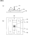
- plasma irradiation is performed so that adhesiveness with the transfer layer is sufficiently developed.
- the mount clip 12 After curing, the mount clip 12 is removed, and an adhesion test sample in which the stud pin 11 is bonded to a three-layer laminate of glass / transfer layer / support film as shown in FIG. 4 is obtained.
- the transferred object 10 of the obtained adhesion test sample was placed on a lower pressure plate 15 of a small table tester EZTest model number EZ-S manufactured by Shimadzu Corporation, and an aluminum fixing plate 13 was used.
- the transferred object 10 is pressed and fixed.
- the aluminum fixing plate 13 is set to be parallel to the side of the transfer body 10, and the distance 14 between the aluminum fixing plates is 15 mm.
- the stud pin 11 is held by the load cell of the tester.
- the stud pin In the tensile test mode, the stud pin is pulled up at a constant speed of 10 mm / min, and the maximum stress when the interface peels between the transfer layer and the support film is defined as the adhesive force at the interface between the support film and the transfer layer.
- the adhesive force varies depending not only on the surface free energy of each material constituting the laminate interface, but also on the interface shape, transfer layer thickness, compositing and post-processing conditions after compositing. Is preferably designed to be in the above preferred range. For example, when a support film having a fine concavo-convex structure on the surface is used, the adhesion between the transfer layer and the support film is higher than when a support film having a flat surface is used.
- the surface free energy of the film is preferably low as long as the transfer layer can be applied.
- the adhesive force between the support film and the transfer layer is lowered, so that an appropriate adhesive force can be obtained by increasing the surface free energy.
- the transfer layer preferably has a hardness of 0.1 to 0.6 GPa.
- the hardness is Mayer hardness, and is measured by pushing a triangular pyramid indenter to a depth corresponding to the transfer layer thickness.
- the hardness is greater than 0.6 GPa, when the transfer layer is pressed and transferred to the transfer target, the transfer layer surface cannot be sufficiently adhered to the transfer target and transfer may not be possible.
- the hardness is less than 0.1 GPa, when the transfer layer is pressed against the transfer target, the transfer layer may be crushed and deformed, or the thickness may be changed.
- the hardness in the present invention is calculated from a load-indentation diagram obtained by measurement by the nanoindentation method. That is, using a regular triangular pyramid shaped diamond indenter, that is, a Barkovic indenter, a static sample was pushed to the same depth as the transfer layer thickness, a load / unload test was performed, and a load-indentation depth diagram (FIG. 6) is acquired. As shown by the following equation, in this load-indentation diagram, the hardness is calculated by dividing the indentation point load by the projected area of the indenter obtained by applying the Oliver-Pharr approximation.
- H the hardness
- P the load
- A the projected contact area
- ⁇ the correction coefficient of the indenter tip shape
- k a coefficient determined from the geometric shape of the indenter, and is 24.56 for the Barkovic indenter.
- hc is an effective contact depth and is represented by the following formula.
- h c h ⁇ P / (dP / dh)
- h is the total displacement to be measured
- dP / dh is the initial gradient 16 at the time of unloading in the load-pushing depth diagram as shown in FIG. 6 obtained by the measurement.
- ⁇ is a constant obtained from the geometric shape of the indenter, and is 0.75 for the Berkovich indenter.
- the indenter is microvibrated during the indentation test, measured by a continuous stiffness measurement method that obtains the response amplitude and phase difference as a function of time, and the hardness-indentation depth diagram (Fig. 7) is obtained. obtain.
- the hardness corresponding to the indentation depth is affected by the hardness of the film as a support for the transfer layer when the indentation depth is deep, and therefore the indentation depth / transfer layer thickness value is 0 to 0.
- region of 125 be the hardness of a transfer layer.
- the surface on the side where the support film is in contact with the transfer layer may be flat or uneven. That is, as shown in FIG. 8A, even if the interface between the transfer film 6 and the transfer layer 8 is flat, a fine uneven shape is formed at the interface between the transfer film 6 and the transfer layer 8 as shown in FIG. There may be seven.
- the interface between the support film and the transfer layer has an uneven shape
- the surface of the transfer layer transferred to the transfer target body has an uneven shape, so that it is possible to provide a covering having an uneven surface on the outermost surface. it can.
- the uneven shape may be a geometric shape or a random shape.
- geometric shapes include prism shapes, moth-eye shapes, inverted truncated cone shapes, hemispherical shapes, cylindrical shapes, and the like.
- the inverted truncated cone shape means an irregular shape in which the shape of the recess is a truncated cone.
- the method for forming the concavo-convex shape on the surface of the support film is not particularly limited, and known methods such as a thermal imprint method, a UV imprint method, coating, and etching can be applied.
- the concavo-convex shape formed on the outermost surface of the transfer layer preferably has a representative pitch in the transfer layer of 0.01 to 10 ⁇ m, and more preferably 0.1 to 8 ⁇ m.
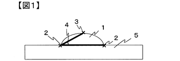
- the representative pitch of the concavo-convex shape in the transfer layer refers to the pitch of the repeated shape when the concavo-convex shape is a geometric shape, and the average value of 10 arbitrarily selected pitches in the case of a random shape.
- the pitch is a horizontal distance 17 between points indicating the respective maximum heights of two adjacent convex portions in the transfer layer. If the convex upper part is flat as shown in FIG. 9B, the horizontal distance 17 between the center points is set as the pitch.
- the representative pitch When the representative pitch is smaller than 0.01 ⁇ m, foreign matter is likely to bite into the recesses between the shapes, and the target structure may not be obtained. On the other hand, when the representative pitch is larger than 10 ⁇ m, the density of the convex shape becomes low, and the effect of the concavo-convex structure may not be sufficiently obtained.
- the aspect ratio of the concavo-convex shape formed on the outermost surface of the transfer layer is preferably 0.01 to 3.0.
- the aspect ratio is a value obtained by dividing the height 19 of the convex portion by the width 18 of the convex shape of the transfer layer, as described with reference to FIG.
- the height 19 of the convex portion is a vertical distance between the adjacent convex portion and the concave portion of the transfer layer.
- the aspect ratio of the uneven shape of the transfer layer is not constant, the average value of the aspect ratios of 10 uneven shapes selected arbitrarily is taken as the value of the aspect ratio.
- the aspect ratio of the concavo-convex shape is smaller than 0.01, the convex shape is very low, and it may be difficult to obtain the effect of the concavo-convex shape.
- the aspect ratio is larger than 3.0, the uneven shape on the support film cannot be filled with the transfer layer, or the releasability between the support film and the transfer layer is lowered, resulting in unevenness during transfer. The shape is easy to tear or fall down.
- the pitch and aspect ratio of the surface irregularities of the transfer layer are measured by cutting the transfer film with a microtome and observing the cross section with a scanning electron microscope.
- the magnification of observation and measurement is 50000 times when the pitch and height of the concavo-convex shape is 0.01 to 0.2 ⁇ m, 20000 times when 0.2 to 2 ⁇ m, and 5000 times when 2 ⁇ m to 5 ⁇ m. In the case of 5 ⁇ m to 10 ⁇ m, it is 2500 times.
- the residual film thickness of the transfer layer is a minimum value of the thickness between the surface of the transfer layer on the side in contact with the transfer target and the surface of the transfer layer on the side in contact with the support film.
- the remaining film thickness of the transfer layer is equal to the thickness of the transfer layer.
- the transfer layer has a concavo-convex shape, the surface of the transfer layer that is in contact with the transfer target and the concave portion of the transfer layer , That is, the distance at which the thickness of the transfer layer is minimized. If it demonstrates using a figure, the distance shown by 20 in Fig.9 (a) is a remaining film thickness.
- the uniformity of the residual film thickness is obtained by dividing the residual film thickness difference indicated by the difference between the maximum value and the minimum value obtained by measuring the residual film thickness at 10 points by the average value of the residual film thickness.
- the uniformity of the remaining film thickness is preferably 25% or less, and more preferably 15% or less.
- the residual film thickness of the transfer layer is measured by cutting the transfer film with a microtome and imaging and measuring the cross section with a scanning electron microscope, as in the method for measuring the transfer layer thickness.
- the magnification of observation and measurement is 50000 times when the remaining film thickness is 0.01 to 0.2 ⁇ m, 20000 times when the remaining film thickness is 0.2 to 2 ⁇ m, 5000 times when 2 ⁇ m to 5 ⁇ m, and 5 ⁇ m to 10 ⁇ m. 2500 times.
- Transfer method A method for transferring a transfer layer to a transfer medium using the transfer film of the present invention will be described.
- the surface of the transfer film on the transfer layer side is brought into contact with the member to be transferred to form a laminate, and the transfer layer can be transferred to the member to be transferred by applying pressure or heating together with pressurization.
- Examples of the pressurizing method at the time of transfer include, but are not limited to, nip rolls and pressurizing with a press.
- the pressure for pressurizing the laminate is preferably 1 kPa to 50 MPa. If the pressure is less than 1 kPa, transfer defects may occur, and if it exceeds 50 MPa, the uneven shape of the support film may be broken or the transferred material may be damaged.
- a buffer material can also be used between the support film of the laminate and a pressure plate, a pressure roll, or the like.
- the cushioning material By using the cushioning material, the transfer layer can be transferred with high accuracy without biting air or the like.
- the buffer material fluorine rubber, silicon rubber, ethylene propylene rubber, isobutylene isoprene rubber, acrylonitrile butadiene rubber, or the like can be used.
- heating can be performed together with pressurization.
- high-temperature heat treatment After transferring the transfer layer to the transfer target, high-temperature heat treatment can be performed in order to advance the polymerization of the siloxane oligomer contained in the transfer layer to vitrify it.
- it may be performed on a laminate of the transfer target / transfer layer / support film, or may be performed on a two-layer stack of the transfer target / transfer layer from which the support film has been peeled off. Good.
- the support film is peeled before the heat treatment in order to obtain a two-layer laminate of the transfer target / transfer layer, the support film is peeled at a temperature equal to or lower than the press temperature after the transfer.
- the temperature at which the support film is peeled is higher than the press temperature, the shape of the transfer layer may be lost, or the peelability between the transfer layer and the support film may be reduced.
- the temperature of the high-temperature heat treatment can be appropriately set according to the heat resistance, chemical resistance and reliability required for the laminate.
- the heat treatment temperature when the transfer layer is used as a protective film by transferring to an inorganic material such as a glass plate or used for imparting irregular shapes on the surface of the glass plate is preferably 150 to 1000 ° C., and preferably 180 to 800 ° C. is more preferable, and 200 to 400 ° C. is most preferable.
- the heat treatment temperature is preferably 700 to 1200 ° C.
- the transfer layer may not be sufficiently densified and may not be used as an etching resist film. If the heat treatment temperature is higher than 1200 ° C., cracks may occur in the transfer layer.
- pre-baking at a temperature lower than the high temperature heat treatment temperature before the treatment can prevent the uneven shape from being deformed by heat.
- the difference between the maximum value and the minimum value of the 10 remaining film thicknesses obtained in this manner was defined as the difference in remaining film thickness.
- the difference of the remaining film thickness was divided by the average value of 10 remaining film thicknesses, and the value expressed as a percentage was defined as the uniformity of the remaining film thickness.
- the transfer layer surface of a 20 mm ⁇ 20 mm transfer film was brought into contact with the glass substrate prepared in (7-1) as a transfer target. Further, a model number F200 manufactured by Kinyo Co., Ltd. was laminated as a buffer material on the support film surface of the transfer film, pressed at a press temperature of 20 ° C. and a press pressure of 1.38 MPa for 10 seconds, and then the support film was peeled off at room temperature.
- the transfer area ratio was calculated by dividing the area of the transfer layer transferred to the transfer medium under the above conditions by the transfer film size of 20 mm ⁇ 20 mm.
- the evaluation criteria for the transfer area ratio were defined and described as follows. A: Transfer area ratio 100%. Good transferability. B: Transfer area ratio of 90% or more and less than 100%. C: Transfer area ratio of 10% or more and less than 90%. D: Transfer area ratio of 0% or more and less than 10%.
- the transfer layer appearance evaluation criteria were defined and evaluated as follows. Good: No crack having a width of 2.0 ⁇ m or more and a length of 5 mm or more in the transfer layer. Defect: There is a crack having a width of 2.0 ⁇ m or more and a length of 5 mm or more in the transfer layer.
- Adhesive force measurement at the interface between the support film and the transfer layer (8-1) Preparation of transfer object Low alkali glass model number 1737 (30 mm ⁇ 30 mm, thickness 1. 1 mm) After removing dust adhering to the surface with a blower, cleaning was performed twice at 45 kHz for 10 minutes using a three-frequency ultrasonic cleaner model number VS-100III manufactured by AS ONE Co., Ltd. in a state immersed in pure water. . Thereafter, the surface of the transferred material was irradiated with plasma at 15000 VAC for 5 minutes using a tabletop vacuum plasma apparatus manufactured by Sakai Semiconductor Co., Ltd.
- Example 1 A film having a thickness of 60 ⁇ m, “Zeonor Film (registered trademark)” model ZF14, manufactured by Nippon Zeon Co., Ltd., which is a cyclic polyolefin resin, and having no irregularities on the surface was used as a support film.
- the surface free energy of the support film was determined by the above method and found to be 34.3 mN / m.
- an OCNL505 model 14000 siloxane sol manufactured by Tokyo Ohka Kogyo Co., Ltd. is applied to the above support film and left to stand at 25 ° C. and 0.1 atm for 3 minutes and dried under reduced pressure, and the support film is composed of a siloxane oligomer.
- a transfer film on which a transfer layer was formed was obtained.
- the thickness of the transfer layer was 9.56 ⁇ m, and the uniformity of the transfer layer thickness was 2%.
- the coatability was good.
- XPS X-ray photoelectron spectroscopy
- the silicon content relative to the total number of carbon, oxygen and silicon atoms in the transfer layer was 25%, and the transfer layer had a hardness of 0.12 GPa.
- the adhesive force at the interface between the film as the support film and the transfer layer was 0.02 MPa.
- Example 2 A transfer film was obtained in the same manner as in Example 1 except that the thickness of the transfer layer was 0.04 ⁇ m. The residual film thickness uniformity of the transfer layer was 23%, and the coating property was good. The transfer layer had a hardness of 0.10 GPa, and an adhesion force at the interface between the support film and the transfer layer was 0.48 MPa.
- Example 3 A transfer film was obtained in the same manner as in Example 1 except that the thickness of the transfer layer was 4.83 ⁇ m. The residual film thickness uniformity of the transfer layer was 11%, and the coating property was very good. The transfer layer had a hardness of 0.12 GPa, and an adhesion force at the interface between the support film and the transfer layer was 0.21 MPa.
- Example 4 A transfer film was obtained in the same manner as in Example 1 except that the thickness of the transfer layer was 0.37 ⁇ m. The residual film thickness uniformity of the transfer layer was 14%, and the coating property was very good. The transfer layer had a hardness of 0.13 GPa, and an adhesion force at the interface between the support film and the transfer layer was 0.38 MPa.
- Example 5 A transfer film was obtained in the same manner as in Example 1 except that a siloxane sol condensed with tetramethoxysilane was used.
- X-ray photoelectron spectroscopy (XPS) measurement shows that the transfer layer has a silicon atom content of 31% of the total number of carbon, oxygen and silicon atoms, the transfer layer thickness is 4.63 ⁇ m, and the residual film thickness is uniform. It was 8%. The coatability was very good.
- the transfer layer had a hardness of 0.15 GPa, and an adhesion force at the interface between the support film and the transfer layer was 0.18 MPa.
- Example 6 A transfer film was obtained in the same manner as in Example 5 except that the thickness of the transfer layer was 0.15 ⁇ m. The residual film thickness uniformity of the transfer layer was 22%. The transfer layer had a hardness of 0.17 GPa, and an adhesion force at the interface between the support film and the transfer layer was 1.69 MPa.
- Example 7 As siloxane sol, colloidal silica particle model number PL-2L (average particle size 17 nm surface area conversion method) manufactured by Fuso Chemical Industry Co., Ltd., obtained by hydrolysis and dehydration condensation of methylsiloxane, phenylsiloxane and dimethylsiloxane are used.
- a transfer film was obtained in the same manner as in Example 1 except that. The content of silicon atoms was 19% with respect to the total number of carbon, oxygen and silicon atoms in the transfer layer as measured by X-ray photoelectron spectroscopy (XPS). The coatability is generally good, the transfer layer thickness is 3.20 ⁇ m, the residual film thickness uniformity is 7%, the transfer layer hardness is 0.19 MPa, and the adhesion between the support film and the transfer layer is 0. It was .81 MPa.
- Example 8 A transfer film was obtained in the same manner as in Example 7 except that the thickness of the transfer layer was 0.09 ⁇ m. The residual film thickness uniformity of the transfer layer was 14%. The transfer layer had a hardness of 0.18 MPa, and an adhesion force at the interface between the support film and the transfer layer was 1.08 MPa.
- Example 9 A film of Toray Film Processing Co., Ltd. “Tretec (registered trademark)” model No. 7721 having a thickness of 45 ⁇ m and having no irregular shape on the surface was used as a support film. The surface free energy was determined by the above method and found to be 33.4 mN / m. Next, a sol prepared by dissolving polysilsesquioxane SR-21 manufactured by Konishi Chemical Industry Co., Ltd. in propylene glycol monomethyl ether acetate was coated on the above support film and dried by heating at 120 ° C. for 1 hour. A transfer film in which a transfer layer made of a siloxane oligomer was formed on the body film was obtained.
- the coatability of the siloxane sol was good.
- the transfer layer had a thickness of 8.65 ⁇ m, the residual film thickness uniformity of the transfer layer was 2%, and the coating property was good.
- the silicon content relative to the total number of carbon, oxygen and silicon atoms in the transfer layer as measured by X-ray photoelectron spectroscopy (XPS) was 9%, and the hardness of the transfer layer was 0.1 GPa.
- the adhesive force at the interface between the support film and the transfer layer was less than 0.02 MPa.
- Example 10 A transfer film was obtained in the same manner as in Example 9 except that the thickness of the transfer layer was 0.64 ⁇ m. The residual film thickness uniformity of the transfer layer was 5%. The transfer layer had a hardness of 0.1 MPa, and an adhesion force at the interface between the support film and the transfer layer was 0.28 MPa.
- Example 11 After the siloxane sol coating, a transfer film was obtained in the same manner as in Example 9 except that the film was left to stand at 25 ° C. and 0.1 atm for 3 minutes and dried under reduced pressure to change the thickness of the transfer layer to 4.21 ⁇ m.
- the transfer layer residual film thickness uniformity was 4%
- the transfer layer hardness was 0.03 MPa
- the adhesion between the support film and the transfer layer was 0.07 MPa.
- Example 12 Example 1 except that a film having a thickness of 60 ⁇ m formed by melt extrusion of a resin of “TOPAS (registered trademark)” model 6013 manufactured by Polyplastics Co., Ltd., which is a cyclic polyolefin resin, was used as a support film. Thus, a transfer film was obtained. The surface free energy of the support film was 38.2 mN / m, and the coating property was very good. The resulting transfer film had a transfer layer thickness of 9.88 ⁇ m and a residual film thickness uniformity of 2%. Moreover, the hardness of the transfer layer was 0.13 GPa, and the adhesive force at the interface between the support film and the transfer layer was less than 0.02 MPa, and could not be measured.
- TOPAS registered trademark
- Example 13 A transfer film was obtained in the same manner as in Example 12 except that the thickness of the transfer layer was 0.06 ⁇ m.
- the residual film thickness uniformity of the transfer layer was 11%, the transfer layer hardness was 0.11 MPa, and the adhesion between the support film and the transfer layer was 1.28 MPa.
- Example 14 Toray Co., Ltd. UV-curable acrylic resin Aronix UV 3701 is applied to a polyester film “Lumirror (registered trademark)” model number U34 with a thickness of 250 ⁇ m to a thickness of 10 ⁇ m. It was. The surface free energy of the UV3701 surface of the support film was determined by the above method and found to be 34.9 mN / m. Next, OCNL505 siloxane sol manufactured by Tokyo Ohka Kogyo Co., Ltd. was coated on the UV3701 surface of the support film and left to stand at 25 ° C. and 0.1 atm for 5 minutes to dry under reduced pressure, and the transfer made of the siloxane oligomer on the support film.
- a transfer film having a layer formed thereon was obtained.
- the coatability was very good.
- XPS X-ray photoelectron spectroscopy
- the silicon content relative to the total number of carbon, oxygen and silicon atoms in the transfer layer was 25%.
- the thickness of the transfer layer was 3.64 ⁇ m, and the uniformity of the remaining film thickness was 20%.
- the hardness of the transfer layer was 0.15 GPa, and the adhesion at the interface between the support film and the transfer layer was 0.69 MPa.
- Example 15 On a polyester film “Lumirror (registered trademark)” model number U34 manufactured by Toray Industries, Inc. having a thickness of 50 ⁇ m, a silicone resin model number ZX-101 manufactured by Fuji Kasei Kogyo Co., Ltd. and “IRGACURE (registered trademark)” model number 250 manufactured by BASF Japan Ltd. The mixture was mixed at a mass ratio of 100 / 3.3 and coated to a thickness of 5 ⁇ m to obtain a support film. The surface free energy of the ZX-101 surface of the support film was determined by the above method and found to be 20.5 mN / m. Next, an OCNL505 siloxane sol manufactured by Tokyo Ohka Kogyo Co., Ltd.
- the transfer layer had a hardness of 0.16 GPa and an adhesion force at the interface between the support film and the transfer layer of 0.05 MPa.
- Example 16 A transfer film was obtained in the same manner as in Example 15 except that the surface of ZX-101 was subjected to corona treatment to obtain a support film.
- the surface free energy of the support film was 64.8 mN / m
- the thickness of the transfer layer was 1.62 ⁇ m
- the uniformity of the remaining film thickness was 3%.
- the transfer layer had a hardness of 0.14 GPa, and an adhesion force at the interface between the support film and the transfer layer was 0.12 MPa.
- Example 17 A transfer film was obtained in the same manner as in Example 1 except that the siloxane sol was coated and dried under reduced pressure, and then heat-treated at 90 ° C. for 1 hour.
- the thickness of the transfer layer was 0.86 ⁇ m, and the uniformity of the remaining film thickness was 6%.
- the hardness of the transfer layer was 0.31 GPa, and the adhesive force at the interface between the support film and the transfer layer was 0.29 MPa.
- Example 18 A transfer film was obtained in the same manner as in Example 1 except that the siloxane sol was coated and dried under reduced pressure, and then heat-treated at 120 ° C. for 1 hour.
- the thickness of the transfer layer was 0.76 ⁇ m, and the uniformity of the remaining film thickness was 7%.
- the transfer layer had a hardness of 0.63 GPa, and an adhesion force at the interface between the support film and the transfer layer was 0.38 MPa.
- Example 19 A transfer film was obtained in the same manner as in Example 1 except that the shape of the surface of the support film in contact with the transfer layer was changed to a prism shape having a pitch of 5 ⁇ m and an aspect ratio of 0.5.
- the surface free energy of the support film was 42.9 mN / m
- the thickness of the transfer layer was 6.96 ⁇ m
- the uniformity of the remaining film thickness was 4%.
- the hardness of the transfer layer was 0.17 GPa
- the adhesive force at the interface between the support film and the transfer layer was 0.17 MPa.
- Example 20 A transfer film was obtained in the same manner as in Example 1 except that the shape of the surface of the support film in contact with the transfer layer was changed to a prism shape having a pitch of 10 ⁇ m and an aspect ratio of 0.5.
- the surface free energy of the support film was 46.4 mN / m
- the thickness of the transfer layer was 8.2 ⁇ m
- the uniformity of the remaining film thickness was 6%.
- the transfer layer had a hardness of 0.14 GPa, and an adhesion force at the interface between the support film and the transfer layer was 1.65 MPa.
- Example 21 A transfer film was obtained in the same manner as in Example 1 except that the shape of the surface of the support film in contact with the transfer layer was changed to a moth-eye shape having a pitch of 0.25 ⁇ m and an aspect ratio of 1.
- the surface free energy of the support film was 45.8 mN / m
- the thickness of the transfer layer was 0.85 ⁇ m
- the uniformity of the remaining film thickness was 12%.
- the transfer layer had a hardness of 0.18 GPa, and an adhesion force at the interface between the support film and the transfer layer was 0.21 MPa.
- Example 22 A transfer film was obtained in the same manner as in Example 1 except that the shape of the surface of the support film in contact with the transfer layer was changed to a truncated cone inverted shape having a pitch of 6.1 ⁇ m and an aspect ratio of 0.08.
- the surface free energy of the support film was 38.2 mN / m
- the thickness of the transfer layer was 0.18 ⁇ m
- the uniformity of the remaining film thickness was 8%.
- the hardness of the transfer layer was 0.16 GPa
- the adhesion between the support film and the transfer layer was 0.33 MPa.
- Example 23 A transfer film was obtained in the same manner as in Example 1 except that the shape of the surface of the support film in contact with the transfer layer was changed to a truncated cone inverted shape having a pitch of 0.25 ⁇ m and an aspect ratio of 2.8.
- the surface free energy of the support film was 72.5 mN / m
- the thickness of the transfer layer was 1.21 ⁇ m
- the uniformity of the remaining film thickness was 3%.
- the transfer layer had a hardness of 0.15 GPa, and an adhesion force at the interface between the support film and the transfer layer was 0.89 MPa.
- Example 3 A transfer film was obtained in the same manner as in Example 1 except that the thickness of the transfer layer was 12 ⁇ m. The residual film thickness uniformity of the transfer layer was 7%, and the transfer layer hardness was 0.17 GPa. The interfacial adhesion between the support film and the transfer layer could not be measured smaller than 0.02 MPa. The transfer layer was transferred to the transfer medium, but cracks occurred due to the shrinkage of the transfer layer.
- Example 5 A transfer film was produced in the same manner as in Example 7 except that the thickness of the transfer layer was 14.6 ⁇ m.
- the transfer film residual film thickness uniformity was 16%
- the transfer layer hardness was 0.20 GPa
- the interfacial adhesion between the support film and the transfer layer was 1.63 MPa.
- the transfer layer was transferred to the transfer target, cracks occurred in the transfer layer due to the shrinkage of the transfer layer.
- a transfer film was obtained in the same manner as in Example 1 except that a mixture of UV curable acrylic resin Aronix UV3701 manufactured by Toagosei Co., Ltd. and tetramethoxysilane was used as the transfer layer.
- the content of silicon atoms relative to the total number of carbon, oxygen and silicon atoms in the transfer layer by XPS was 3%.
- the thickness of the transfer layer was 7.39 ⁇ m, and the residual film thickness uniformity of the transfer layer was 9%.
- the transfer layer had a hardness of 0.15 GPa.
- the interfacial adhesion force between the support film and the transfer layer was larger than the adhesion force between the glass surface as the transfer target and the transfer layer, and could not be measured because peeling was not possible.
- Tables 2 and 3 show the results of conducting transferability confirmation experiments on the transfer films prepared in Examples 1 to 24 and Comparative Examples 1 to 6.
- each of Examples 1 to 17 and 19 to 22 showed good transferability, and a siloxane layer with few defects could be formed on the transfer target.
- Example 18 the appearance of the transfer film was good, but since the transfer layer was hard, the followability to the substrate was low, and the transfer area ratio was low.
- Example 23 the appearance of the transfer film was good, but there were defects due to repelling in the transfer layer formation.
- Comparative Examples 1 and 6 the transfer layer of the transfer film could not be transferred.
- Comparative Examples 2 and 4 a transfer film could not be obtained due to repelling during the formation of the transfer layer.
- the siloxane oligomer is siloxane
- the silicon atom content relative to the total number of atoms of carbon, oxygen, and silicon is the silicon atom content
- the adhesion force at the interface between the support film and the transfer layer was abbreviated as adhesion.
- a siloxane layer excellent in heat resistance and light resistance and having few defects can be imparted to a large-area transferred object by a simple manufacturing process.
- a siloxane layer having a fine concavo-convex shape on a large area to be transferred with a simple manufacturing process without generating cracks. Can be granted.
Landscapes
- Engineering & Computer Science (AREA)
- Chemical & Material Sciences (AREA)
- Mechanical Engineering (AREA)
- Manufacturing & Machinery (AREA)
- Polymers & Plastics (AREA)
- Organic Chemistry (AREA)
- Medicinal Chemistry (AREA)
- Chemical Kinetics & Catalysis (AREA)
- Health & Medical Sciences (AREA)
- Physics & Mathematics (AREA)
- Materials Engineering (AREA)
- Condensed Matter Physics & Semiconductors (AREA)
- Electromagnetism (AREA)
- General Physics & Mathematics (AREA)
- Computer Hardware Design (AREA)
- Microelectronics & Electronic Packaging (AREA)
- Power Engineering (AREA)
- Laminated Bodies (AREA)
- Coating Of Shaped Articles Made Of Macromolecular Substances (AREA)
Abstract
Description
支持体としては、厚さが5~500μmのフィルムが好ましく、厚さは40~300μmがより好ましい。フィルムの厚さが5μmより薄い場合、転写層を転写する際によれてしまい、被転写体を正確に被覆できない場合がある。一方、フィルムの厚さが500μmを超える場合は、支持体フィルムが剛直になり、被覆体に追従できなくなる場合がある。該支持体フィルムの材質は、転写層の溶媒除去や、被覆体への転写の際の加熱に耐えうるものであれば特に限定されず、例えばポリエチレンテレフタレート、ポリエチレン-2,6-ナフタレート、ポリプロピレンテレフタレート、ポリブチレンテレフタレート等のポリエステル系樹脂;ポリエチレン、ポリスチレン、ポリプロピレン、ポリイソブチレン、ポリブテン、ポリメチルペンテン等のポリオレフィン系樹脂;環状ポリオレフィン系樹脂、ポリアミド系樹脂、ポリイミド系樹脂、ポリエーテル系樹脂、ポリエステルアミド系樹脂、ポリエーテルエステル系樹脂、アクリル系樹脂、ポリウレタン系樹脂、ポリカーボネート系樹脂、あるいはポリ塩化ビニル系樹脂等を用いることができる。転写層の原料であるシロキサンゾルの塗工性、および、転写層と支持体フィルムとの離型性を両立できる観点から、ポリオレフィン系樹脂やアクリル系樹脂が好ましい。 [Support]
The support is preferably a film having a thickness of 5 to 500 μm, and more preferably 40 to 300 μm. When the thickness of the film is less than 5 μm, the film is swayed when the transfer layer is transferred, and the transferred object may not be covered accurately. On the other hand, when the thickness of the film exceeds 500 μm, the support film becomes rigid and may not be able to follow the covering. The material of the support film is not particularly limited as long as it can withstand the solvent removal of the transfer layer and the heating at the time of transfer to the coating. For example, polyethylene terephthalate, polyethylene-2,6-naphthalate, polypropylene terephthalate Polyester resins such as polybutylene terephthalate; Polyolefin resins such as polyethylene, polystyrene, polypropylene, polyisobutylene, polybutene and polymethylpentene; Cyclic polyolefin resins, polyamide resins, polyimide resins, polyether resins, polyesteramides Resin, polyether ester resin, acrylic resin, polyurethane resin, polycarbonate resin, polyvinyl chloride resin, or the like can be used. Polyolefin resins and acrylic resins are preferred from the viewpoints of achieving both the coatability of the siloxane sol that is the raw material of the transfer layer and the releasability between the transfer layer and the support film.
(γS d・γL d)1/2+(γS p・γL p)1/2+(γS h・γL h)1/2=(1+cosθ)/2
ここで、γL d、γL pおよびγL hは、それぞれ測定液の分散力成分、極性力成分および水素結成分の値(既知)、θは測定面上での測定液の接触角、また、γS d、γS pおよびγS hは、それぞれ測定表面の分散力成分、極性力成分および水素結合成分の値を表す。なお、表面自由エネルギーおよびその各成分が既知の4種類の液体としては、純水、エチレングリコール、ホルムアミド、ヨウ化メチレンを用いる。各成分の値は表1に示す。 Here, the surface free energy is represented by the sum of the values of the dispersion force component, the polar force component, and the hydrogen bond component. The surface free energy of the measurement target surface is determined by measuring the contact angle with the measurement target surface for four types of liquids whose surface free energy and its components (dispersion force component, polar force component, hydrogen bond component) are known, It can be calculated by substituting the value of each component of the liquid and the value of the obtained contact angle into the following equation derived from the extended Fowkes equation and the Young equation, and solving the simultaneous equations.
(Γ S d · γ L d ) 1/2 + (γ S p · γ L p) 1/2 + (γ S h · γ L h) 1/2 = (1 + cosθ) / 2
Here, γ L d , γ L p and γ L h are the values of dispersion force component, polar force component and hydrogenation component (known) of the measurement liquid, respectively, θ is the contact angle of the measurement liquid on the measurement surface, Further, γ S d, γ S p and gamma S h, the dispersion force component of each measuring surface, representing the value of the polar force component and hydrogen bonding component. In addition, pure water, ethylene glycol, formamide, and methylene iodide are used as the four types of liquids whose surface free energy and its components are known. The value of each component is shown in Table 1.

表面自由エネルギー算出のための接触角測定は、協和界面科学株式会社製接触角計CA-X型で、手動3測定点計測による液滴法(θ/2法)で行う。まず、測定試料表面が水平になるように試料台にセットする。測定液として純水を用い、シリンジを用いて純水0.4μLの液滴を測定試料の測定表面に付着させる。付着させてから5秒後に、液滴画像をフリーズさせて、その液滴の接触角を測定する。接触角は手動3測定点計測によるため、図1に示すような試料5の上の液滴1の両端の点2と、頂点3を選択して、その液滴のθ/2 (4)を算出し、θ/2の2倍の値を接触角とする。測定は5回繰り返し、その平均値を測定サンプルの接触角の値とする。ただし、測定表面に汚れやキズがある場合は正確な値を得ることができないため、測定した5回の接触角の標準偏差が3.0を超えた場合は再度測定するものとする。エチレングリコール、ホルムアミドおよびヨウ化メチレンの3種類の測定液についても、純水で行ったのと同様にして、接触角を測定する。次いで、上記4種類の液体の接触角測定値を前述の式に代入して表面自由エネルギーの各成分の実測値([γS d]SE,[γS p]SE,[γS h]SE)を算出する。 (I) Contact angle measurement of the measurement sample and calculation of surface free energy Contact angle measurement for calculating surface free energy is a contact angle meter CA-X manufactured by Kyowa Interface Science Co., Ltd. By the method (θ / 2 method). First, the measurement sample surface is set on the sample stage so that it is horizontal. Pure water is used as the measurement liquid, and a droplet of 0.4 μL of pure water is attached to the measurement surface of the measurement sample using a syringe. Five seconds after deposition, the droplet image is frozen and the contact angle of the droplet is measured. Since the contact angle is measured manually at three measurement points, the
厚さ100μmの東レ株式会社製ポリエステルフィルム“ルミラー(登録商標)”型番U426の表面を補正用の基準サンプルとした。補正用基準サンプル表面について、前記(i)と同じ温湿度環境下で、純水、エチレングリコール、ホルムアミドおよびヨウ化メチレンの4種類の測定液の接触角を前記(i)と同一の手順、かつ、同一の環境下で行い、表面自由エネルギーの各成分の実測値([γS d]RE,[γS p]RE,[γS h]RE)を算出する。 (Ii) Measurement of contact angle of standard sample and calculation of surface free energy The surface of polyester film “Lumirror (registered trademark)” model number U426 having a thickness of 100 μm manufactured by Toray Industries, Inc. was used as a reference sample for correction. With respect to the reference sample surface for correction, in the same temperature and humidity environment as in the above (i), the contact angle of four kinds of measurement liquids of pure water, ethylene glycol, formamide and methylene iodide was set in the same procedure as in the above (i), and carried out under the same environment, measured values of each component of the surface free energy ([γ S d] RE, [γ S p] RE, [γ S h] RE) is calculated.
ここで、補正用のサンプルである厚さ100μmの東レ株式会社製ポリエステルフィルム“ルミラー(登録商標)”型番U426の表面の分散力成分の標準値([γS d]RT)、極性力成分の標準値([γS p]RT)、水素結合成分の標準値([γS h]RT)はそれぞれ27.1mN/m、10.8mN/m、7.0mN/mであるので、この値を用いて下記式により、前記(i)により求めた実測値([γS d]SE,[γS p]SE,[γS h]SE)を補正し、測定サンプルの各成分値([γS d]ST,[γS p]ST,[γS h]ST)を得る。
[γS d]ST=[γS d]SE-([γS d]RE-[γS d]RT)
[γS p]ST=[γS p]SE-([γS p]RE-[γS p]RT)
[γS h]ST=[γS h]SE-([γS h]RE-[γS h]RT)
なお、本発明において標準サンプルの各成分の標準値([γS d]RT,[γS p]RT,[γS h]RT)は、標準サンプルを室温30℃湿度35%、室温23℃湿度32%、室温24℃湿度28%の3環境下で測定し、それぞれ前記(i)の方法で算出した表面自由エネルギーの各成分を平均して求めた値を用いている。 (Iii) Correction of measured value of each component of surface free energy Here, standard of dispersion force component of surface of polyester film “Lumirror (registered trademark)” model number U426 manufactured by Toray Industries Inc. with a thickness of 100 μm, which is a sample for correction The value ([γ S d ] RT), the standard value of the polar force component ([γ S p ] RT), and the standard value of the hydrogen bond component ([γ S h ] RT) are 27.1 mN / m and 10.8 mN, respectively. / M, 7.0 mN / m, and using this value, the measured values ([γ S d ] SE, [γ S p ] SE, [γ S h ]] obtained from the above (i) by the following formula: SE) is corrected, and each component value ([γ S d ] ST, [γ S p ] ST, [γ S h ] ST) of the measurement sample is obtained.
[Γ S d ] ST = [γ S d ] SE − ([γ S d ] RE− [γ S d ] RT)
[Γ S p ] ST = [γ S p ] SE − ([γ S p ] RE− [γ S p ] RT)
[Γ S h ] ST = [γ S h ] SE − ([γ S h ] RE− [γ S h ] RT)
In the present invention, the standard values ([γ S d ] RT, [γ S p ] RT, [γ S h ] RT) of each component of the standard sample are the standard sample at room temperature 30 ° C., humidity 35%, and room temperature 23 ° C. Measurement was performed under three environments of humidity 32% and room temperature 24 ° C. and humidity 28%, and values obtained by averaging the components of the surface free energy calculated by the method (i) were used.
本発明の転写フィルムにおいて、支持体フィルム上に積層された転写層にはシロキサンオリゴマーが含まれる。転写層の個別の成分についての詳細は後述するが、転写層のX線光電子分光(XPS)測定による炭素、酸素およびケイ素の各原子数の合計に対するケイ素原子数の含有率(以降単にケイ素原子の含有率と記すこともある)は5~33%であることが好ましく、8~30%であることがより好ましい。ケイ素原子の含有率が5%未満の場合、転写層に含まれるシロキサンオリゴマー中のシロキサン結合が少なく、有機物の割合が高い構造となるため、転写層において高温での分解や紫外線による黄変が発生する。また、ケイ素原子の含有率が33%を超えると、転写層に含まれるシロキサンオリゴマーの構造がガラスに非常に近くなり、被転写体との密着性が低下するおそれがある。また、転写層中のシロキサンオリゴマーの含有量は、50~99質量%であることが好ましい。 [Transfer layer composition]
In the transfer film of the present invention, the transfer layer laminated on the support film contains a siloxane oligomer. Although details of the individual components of the transfer layer will be described later, the content of silicon atoms relative to the total number of carbon, oxygen, and silicon atoms (hereinafter simply referred to as silicon atoms) by X-ray photoelectron spectroscopy (XPS) measurement of the transfer layer. The content may also be described as 5 to 33%, more preferably 8 to 30%. When the silicon atom content is less than 5%, the siloxane oligomer contained in the transfer layer contains few siloxane bonds and has a high organic content, resulting in decomposition at high temperatures and yellowing due to ultraviolet rays in the transfer layer. To do. On the other hand, if the silicon atom content exceeds 33%, the structure of the siloxane oligomer contained in the transfer layer is very close to that of glass, and the adhesion to the transfer medium may be reduced. The content of the siloxane oligomer in the transfer layer is preferably 50 to 99% by mass.
転写層には、上述のようにシロキサンオリゴマーが含まれる。ここで、シロキサンオリゴマーとは、2つ以上の連続したシロキサン結合を有するポリオルガノシロキサン骨格を構造内に含むシロキサン化合物を指す。また、該シロキサンオリゴマーには、部分構造としてケイ素原子に直接結合する有機官能基をもたないシリカ構造を一部含んでいても良い。該シロキサンオリゴマーの重量平均分子量は、特に制限されないが、GPCで測定されるポリスチレン換算で500~100000であることが好ましい。シロキサンオリゴマーは、下記一般式(1)で表されるオルガノシランの1種類以上を加水分解・重縮合反応させることによって合成されるシロキサンゾルを、加熱加圧によって固化して合成される。 [Siloxane oligomer]
The transfer layer contains a siloxane oligomer as described above. Here, the siloxane oligomer refers to a siloxane compound having a polyorganosiloxane skeleton having two or more continuous siloxane bonds in the structure. In addition, the siloxane oligomer may partially include a silica structure having no organic functional group directly bonded to a silicon atom as a partial structure. The weight average molecular weight of the siloxane oligomer is not particularly limited, but is preferably 500 to 100,000 in terms of polystyrene measured by GPC. The siloxane oligomer is synthesized by solidifying a siloxane sol synthesized by hydrolysis and polycondensation reaction of one or more types of organosilane represented by the following general formula (1) by heating and pressing.
式中、R1は水素、炭素数1~10のアルキル基、炭素数2~10のアルケニル基および炭素数6~15のアリール基のいずれかを表し、複数のR1はそれぞれ同じでも異なっていてもよい。R2は水素、炭素数1~6のアルキル基、炭素数1~6のアシル基および炭素数6~15のアリール基のいずれかを表し、複数のR2はそれぞれ同じでも異なっていてもよい。nは0から3の整数を表す。 (R1) n -Si- (OR2) 4-n (1)
In the formula, R1 represents any one of hydrogen, an alkyl group having 1 to 10 carbon atoms, an alkenyl group having 2 to 10 carbon atoms, and an aryl group having 6 to 15 carbon atoms, and a plurality of R1 may be the same or different. Good. R2 represents any one of hydrogen, an alkyl group having 1 to 6 carbon atoms, an acyl group having 1 to 6 carbon atoms, and an aryl group having 6 to 15 carbon atoms, and a plurality of R2 may be the same or different. n represents an integer of 0 to 3.
支持体フィルム上に転写層を積層する方法としては、膜厚の調整がしやすく、支持体フィルムの厚み等に影響を受けにくいため、溶媒で希釈したシロキサンゾルを支持体フィルム上に塗工し、乾燥する方法が好ましい。 [Lamination of transfer layer]
As a method of laminating the transfer layer on the support film, it is easy to adjust the film thickness and is not easily affected by the thickness of the support film, so apply a siloxane sol diluted with a solvent on the support film. A method of drying is preferred.
転写層の厚みは0.01~10μmであることが好ましく、0.1~5μmであることがより好ましい。転写層の厚みが0.01μmより薄い場合、シロキサンゾルの塗工においてハジキが発生しやすく、転写層に欠点が生じる場合がある。一方、転写層の厚みが10μmより厚い場合、転写層が硬化する際の膜応力によって、転写層にクラックが発生する場合がある。なお、転写層の厚みとは、転写フィルムにおける厚みであって、上記の転写層の積層工程において乾燥した後の厚みであることは言うまでもない。転写層の厚みは、転写フィルムをミクロトームで切削し、その断面を走査型電子顕微鏡(以下SEMと略記することもある)で撮像し、測定する。 [Thickness of transfer layer]
The thickness of the transfer layer is preferably from 0.01 to 10 μm, more preferably from 0.1 to 5 μm. When the thickness of the transfer layer is less than 0.01 μm, repelling is likely to occur in the application of the siloxane sol, and a defect may occur in the transfer layer. On the other hand, when the thickness of the transfer layer is greater than 10 μm, cracks may occur in the transfer layer due to film stress when the transfer layer is cured. It should be noted that the thickness of the transfer layer is the thickness of the transfer film and is the thickness after drying in the transfer layer laminating step. The thickness of the transfer layer is measured by cutting the transfer film with a microtome, and imaging the cross section with a scanning electron microscope (hereinafter sometimes abbreviated as SEM).
支持体フィルムと転写層との界面の密着力(単に密着力と記す場合もある)は、0.02MPa~1.50MPaであることが好ましい。0.02MPaよりも密着力が弱い場合、支持体フィルムと転写層が剥離して、転写フィルムとしてハンドリングできず、実質的に被転写体への転写作業をできない場合がある。一方、1.50MPaよりも密着力が強い場合、転写層が支持体フィルムから剥がれず、被転写体に転写層を転写することができない場合がある。 [Adhesion at interface between support film and transfer layer]
The adhesion force at the interface between the support film and the transfer layer (sometimes simply referred to as adhesion force) is preferably 0.02 MPa to 1.50 MPa. When the adhesive force is weaker than 0.02 MPa, the support film and the transfer layer are peeled off and cannot be handled as the transfer film, and the transfer operation to the transfer target material may be substantially impossible. On the other hand, when the adhesion is stronger than 1.50 MPa, the transfer layer may not be peeled off from the support film, and the transfer layer may not be transferred to the transfer target.
転写層は、硬さが0.1~0.6GPaであることが好ましい。詳細な測定方法は後述するが、ここでいう硬さはMayer硬度のことであり、三角錐圧子を転写層厚みに対応する深さまで押し込むことにより測定される硬さである。硬さが0.6GPaより大きい場合は、転写層を被転写体に押圧して転写する際に、転写層表面が被転写体に十分に密着できず、転写できないおそれがある。一方、硬さが0.1GPaより小さい場合は、転写層を被転写体に押圧した際に、転写層が押しつぶされて変形したり、厚みが変わったりするおそれがある。 [Hardness of transfer layer]
The transfer layer preferably has a hardness of 0.1 to 0.6 GPa. Although a detailed measuring method will be described later, the hardness here is Mayer hardness, and is measured by pushing a triangular pyramid indenter to a depth corresponding to the transfer layer thickness. When the hardness is greater than 0.6 GPa, when the transfer layer is pressed and transferred to the transfer target, the transfer layer surface cannot be sufficiently adhered to the transfer target and transfer may not be possible. On the other hand, when the hardness is less than 0.1 GPa, when the transfer layer is pressed against the transfer target, the transfer layer may be crushed and deformed, or the thickness may be changed.
H=P/A
A=ηkhc
ここで、Hは硬さ、Pは荷重、Aは接触投影面積、ηは圧子先端形状の補正係数、kは圧子の幾何学形状から決まる係数であり、バーコビッチ圧子では24.56である。また、hcは有効接触深さであり下記式で表される。
hc=h-εP/(dP/dh)
ここで、hは測定される全変位、dP/dhは測定によって得られた図6に示すような荷重-押し込み深さ線図における除荷時の初期勾配16である。また、εは圧子の幾何形状から求まる定数であり、バーコビッチ圧子では0.75となる。 The hardness in the present invention is calculated from a load-indentation diagram obtained by measurement by the nanoindentation method. That is, using a regular triangular pyramid shaped diamond indenter, that is, a Barkovic indenter, a static sample was pushed to the same depth as the transfer layer thickness, a load / unload test was performed, and a load-indentation depth diagram (FIG. 6) is acquired. As shown by the following equation, in this load-indentation diagram, the hardness is calculated by dividing the indentation point load by the projected area of the indenter obtained by applying the Oliver-Pharr approximation.
H = P / A
A = ηkh c
Here, H is the hardness, P is the load, A is the projected contact area, η is the correction coefficient of the indenter tip shape, k is a coefficient determined from the geometric shape of the indenter, and is 24.56 for the Barkovic indenter. Moreover, hc is an effective contact depth and is represented by the following formula.
h c = h−εP / (dP / dh)
Here, h is the total displacement to be measured, and dP / dh is the
支持体フィルムが転写層と接する側の表面は平坦でも凹凸形状であっても良い。すなわち図8(a)に示すように、転写フィルム6と転写層8の界面が平坦であっても、図8(b)に示すように転写フィルム6と転写層8の界面に微細な凹凸形状7があっても良い。支持体フィルムと転写層の界面が凹凸形状である場合、被転写体に転写された転写層の表面が凹凸形状を有することになるので、最表面が凹凸形状を有する被覆体を提供することができる。 [Form of the surface of the support film on the side in contact with the transfer layer]
The surface on the side where the support film is in contact with the transfer layer may be flat or uneven. That is, as shown in FIG. 8A, even if the interface between the
転写層の残膜厚みとは、転写層の被転写体と接する側の表面と、転写層の支持体フィルムと接する側の表面との間の厚みの極小値である。転写層が平坦な場合は、転写層の残膜厚みは、転写層の厚みと等しくなるが、転写層が凹凸形状を有する場合は、転写層の被転写体と接する側の表面と転写層凹部の距離、すなわち、転写層の厚みが極小になる距離を残膜厚みとする。図を用いて説明すると、図9(a)において、20で示される距離が残膜厚みである。また、残膜厚みを10点計測して得られた最大値と最小値の差で示される残膜厚み差を、残膜厚みの平均値で除算して得られる値を残膜厚みの均一性とする。残膜厚みの均一性は25%以下が好ましく、15%以下がより好ましい。残膜厚みの均一性が25%を超える場合、転写層を被転写体と接触させて押圧する際に転写ムラや欠点の発生原因となったり、被転写体に形成した凹凸形状をエッチング処理する際に形状サイズが不均一になったりするおそれがある。なお、転写層の残膜厚みは、転写層厚みの測定方法と同様に、転写フィルムをミクロトームで切削し、その断面を走査型電子顕微鏡で撮像および計測することにより測定する。観察および測定の倍率は、残膜厚みが0.01~0.2μmの場合は50000倍、0.2~2μmの場合は20000倍、2μm~5μmの場合は5000倍、5μm~10μmの場合は2500倍とする。 [Uniformity of transfer layer residual film thickness]
The residual film thickness of the transfer layer is a minimum value of the thickness between the surface of the transfer layer on the side in contact with the transfer target and the surface of the transfer layer on the side in contact with the support film. When the transfer layer is flat, the remaining film thickness of the transfer layer is equal to the thickness of the transfer layer. However, when the transfer layer has a concavo-convex shape, the surface of the transfer layer that is in contact with the transfer target and the concave portion of the transfer layer , That is, the distance at which the thickness of the transfer layer is minimized. If it demonstrates using a figure, the distance shown by 20 in Fig.9 (a) is a remaining film thickness. In addition, the uniformity of the residual film thickness is obtained by dividing the residual film thickness difference indicated by the difference between the maximum value and the minimum value obtained by measuring the residual film thickness at 10 points by the average value of the residual film thickness. And The uniformity of the remaining film thickness is preferably 25% or less, and more preferably 15% or less. When the uniformity of the residual film thickness exceeds 25%, when the transfer layer is brought into contact with the transfer object and pressed, it causes transfer unevenness and defects, or the uneven shape formed on the transfer object is etched. In some cases, the shape size may be uneven. The residual film thickness of the transfer layer is measured by cutting the transfer film with a microtome and imaging and measuring the cross section with a scanning electron microscope, as in the method for measuring the transfer layer thickness. The magnification of observation and measurement is 50000 times when the remaining film thickness is 0.01 to 0.2 μm, 20000 times when the remaining film thickness is 0.2 to 2 μm, 5000 times when 2 μm to 5 μm, and 5 μm to 10 μm. 2500 times.
本発明の転写フィルムを用い、転写層を被転写体に転写する方法について述べる。転写フィルムの転写層の側の面を被転写体に接触させて積層体とし、加圧するか、または加圧とともに加熱することにより、転写層を被転写体に転写することができる。転写の際の加圧方法としては、例えば、ニップロールや、プレス機による加圧などが挙げられるがこれらに限定されるものではない。積層体を加圧する圧力は1kPa~50MPaが好ましい。圧力が1kPa未満であると、転写欠点が生じる場合があり、50MPaを超えると、支持体フィルムの凹凸形状が崩れたり、被転写体が破損したりする場合がある。また、加圧する際には、該積層体の支持体フィルムと加圧プレートや加圧ロール等との間に緩衝材を用いることもできる。緩衝材を使用することによって空気等を噛み込むことなく精度よく転写層を転写できる。緩衝材としては、フッ素ゴム、シリコンゴム、エチレンプロピレンゴム、イソブチレンイソプレンゴム、アクリロニトリルブタジエンゴムなどが使用できる。また、被転写体に転写層を十分に密着させるために、加圧とともに加熱することもできる。 [Transfer method]
A method for transferring a transfer layer to a transfer medium using the transfer film of the present invention will be described. The surface of the transfer film on the transfer layer side is brought into contact with the member to be transferred to form a laminate, and the transfer layer can be transferred to the member to be transferred by applying pressure or heating together with pressurization. Examples of the pressurizing method at the time of transfer include, but are not limited to, nip rolls and pressurizing with a press. The pressure for pressurizing the laminate is preferably 1 kPa to 50 MPa. If the pressure is less than 1 kPa, transfer defects may occur, and if it exceeds 50 MPa, the uneven shape of the support film may be broken or the transferred material may be damaged. Moreover, when pressurizing, a buffer material can also be used between the support film of the laminate and a pressure plate, a pressure roll, or the like. By using the cushioning material, the transfer layer can be transferred with high accuracy without biting air or the like. As the buffer material, fluorine rubber, silicon rubber, ethylene propylene rubber, isobutylene isoprene rubber, acrylonitrile butadiene rubber, or the like can be used. In addition, in order to sufficiently adhere the transfer layer to the transfer target, heating can be performed together with pressurization.
被転写体に転写層を転写した後、転写層に含まれるシロキサンオリゴマーの重合を進行させてガラス化するために高温熱処理を行うこともできる。高温熱処理を行う際は、被転写体/転写層/支持体フィルムの積層体に対して行っても、支持体フィルムを剥離した被転写体/転写層の2層積層体に対して行ってもよい。被転写体/転写層の2層積層体にするために支持体フィルムを熱処理前に剥離する場合は、転写後、プレス温度以下で支持体フィルムを剥離する。支持体フィルムを剥離する際の温度が、プレス温度より高い場合、転写層の形状が崩れたり、転写層と支持体フィルムの間の剥離性が低下したりするおそれがある。前記高温熱処理の温度は、積層体に求められる耐熱性、耐薬品性および信頼性に応じて適宜設定することができる。例えば、ガラス板等の無機系材料に転写することで、転写層を保護膜としたり、ガラス板表面の凹凸形状付与に使用したりする場合の熱処理温度は、150~1000℃が好ましく、180~800℃がより好ましく、200~400℃がもっとも好ましい。150℃未満で熱処理した場合、シロキサンオリゴマーの縮合が十分に進行せず、十分に固化できなかったり耐熱性が悪くなったりする場合がある。一方、1000℃より高い温度で熱処理した場合、転写層にクラックが発生したり、凹凸形状が崩れてしまったりする場合がある。一方、エッチングレートの低い無機材料または結晶材料からなる被転写体に転写した転写層をエッチングレジスト膜として使用する場合は、被転写体よりも転写層のエッチングレートを低くする必要がある。そのためには、転写層中の有機成分を焼散させて緻密な二酸化ケイ素膜にすることが有効であるため、熱処理温度は700~1200℃であることが好ましい。熱処理温度が700℃未満の場合、転写層が十分に緻密化されず、エッチングレジスト膜として使用できない場合がある。熱処理温度が、1200℃より高い場合、転写層にクラックが発生するおそれがある。高温熱処理に際しては、処理前に高温熱処理温度よりも低い温度でプレベークすることで熱による凹凸形状の崩れを防止することもできる。 [Post-transfer processing]
After transferring the transfer layer to the transfer target, high-temperature heat treatment can be performed in order to advance the polymerization of the siloxane oligomer contained in the transfer layer to vitrify it. When performing the high-temperature heat treatment, it may be performed on a laminate of the transfer target / transfer layer / support film, or may be performed on a two-layer stack of the transfer target / transfer layer from which the support film has been peeled off. Good. In the case where the support film is peeled before the heat treatment in order to obtain a two-layer laminate of the transfer target / transfer layer, the support film is peeled at a temperature equal to or lower than the press temperature after the transfer. When the temperature at which the support film is peeled is higher than the press temperature, the shape of the transfer layer may be lost, or the peelability between the transfer layer and the support film may be reduced. The temperature of the high-temperature heat treatment can be appropriately set according to the heat resistance, chemical resistance and reliability required for the laminate. For example, the heat treatment temperature when the transfer layer is used as a protective film by transferring to an inorganic material such as a glass plate or used for imparting irregular shapes on the surface of the glass plate is preferably 150 to 1000 ° C., and preferably 180 to 800 ° C. is more preferable, and 200 to 400 ° C. is most preferable. When heat treatment is performed at a temperature lower than 150 ° C., the condensation of the siloxane oligomer does not proceed sufficiently and may not be sufficiently solidified or heat resistance may deteriorate. On the other hand, when heat treatment is performed at a temperature higher than 1000 ° C., cracks may occur in the transfer layer, or the uneven shape may be lost. On the other hand, when a transfer layer transferred to a transfer material made of an inorganic material or a crystal material having a low etching rate is used as an etching resist film, the transfer layer needs to have a lower etching rate than the transfer material. For this purpose, it is effective to burn the organic components in the transfer layer to form a dense silicon dioxide film, and therefore the heat treatment temperature is preferably 700 to 1200 ° C. When the heat treatment temperature is less than 700 ° C., the transfer layer may not be sufficiently densified and may not be used as an etching resist film. If the heat treatment temperature is higher than 1200 ° C., cracks may occur in the transfer layer. In the high temperature heat treatment, pre-baking at a temperature lower than the high temperature heat treatment temperature before the treatment can prevent the uneven shape from being deformed by heat.
協和界面科学株式会社製接触角計CA-X型を使用して、支持体フィルムの接触角を測定し、前記の方法により、基準値で補正した表面自由エネルギーを求めた。なお、測定においてはそれぞれ5回ずつ測定し、その平均値を接触角とした。 (1) Evaluation of surface free energy of support film Using contact angle meter CA-X manufactured by Kyowa Interface Science Co., Ltd., the contact angle of the support film was measured and corrected with the reference value by the above method. The surface free energy was determined. In addition, in each measurement, it measured 5 times each and the average value was made into the contact angle.
30mm×30mmの支持体フィルムに表2に記載の各転写層厚みになるようシロキサンゾルを塗工し、その塗工性を評価した。転写層厚みが5μm以下の場合は、ミカサ株式会社製スピンコーター型番1H-DX2を使用して、転写層厚みが5μmを超える場合はベーカーアプリケーターを使用して塗工した。
塗工性は次の基準で評価した。
A:ハジキがなく、塗工性良好。
B:ハジキがあるが、塗工可能。
C:ハジキや転写層のクラックにより転写層を形成できない、もしくは、塗工不可能。 (2) Evaluation of coating property and evaluation of transfer property Siloxane sol was applied to a support film of 30 mm x 30 mm so as to have the thickness of each transfer layer described in Table 2, and the coating property was evaluated. When the transfer layer thickness was 5 μm or less, coating was performed using a spin coater model 1H-DX2 manufactured by Mikasa Co., Ltd., and when the transfer layer thickness exceeded 5 μm, a Baker applicator was used.
The coatability was evaluated according to the following criteria.
A: There is no cissing and coating properties are good.
B: There is repelling, but coating is possible.
C: The transfer layer cannot be formed or coated due to repelling or cracks in the transfer layer.
転写層の炭素、酸素およびケイ素の各原子数の合計に対するケイ素原子の含有率は、アルバック-ファイ株式会社製走査型X線光電子分光分析装置PHI Quantera SXM(X線源AlKα)により測定した。測定データはC1s結合エネルギーに対応するピークを284.4eVに補正し、Si2pに対応する102~103eV付近のピークおよびO1sに対応する530~535eV付近のピークに着目して、相対感度係数(RSF)を用いて定量した。 (3) Measurement of silicon atom content with respect to the total number of carbon, oxygen and silicon atoms by XPS (X-ray photoelectron spectroscopy) Content of silicon atom with respect to the total number of carbon, oxygen and silicon atoms in the transfer layer Was measured with a scanning X-ray photoelectron spectrometer PHI Quantera SXM (X-ray source AlKα) manufactured by ULVAC-PHI Co., Ltd. In the measurement data, the peak corresponding to the C1s binding energy is corrected to 284.4 eV, and the relative sensitivity coefficient (RSF) is focused on the peak near 102 to 103 eV corresponding to Si2p and the peak near 530 to 535 eV corresponding to O1s. Was quantified.
(4-1)転写層の厚みと残膜厚みの測定
株式会社ミクロトーム研究所製ロータリーミクロトーム型番RMSで転写フィルムを切削し、その断面をTOPCON社製miniSEM型番ABT-32で観察および測定した。倍率とその測定方法は前記の条件とした。
(4-2)残膜厚み均一性の算出
転写層が平坦な場合は、転写層の任意の10点について厚みを計測した。転写層が凹凸形状を有する場合は、厚みの極小点を任意に10点選んで計測した。このようにして得られた10点の残膜厚みの、最大値と最小値の差を残膜厚みの差とした。この残膜厚みの差を、10点の残膜厚みの平均値で除して百分率表示した値を残膜厚みの均一性とした。 (4) Evaluation of Transfer Layer Thickness and Residual Film Thickness (4-1) Measurement of Transfer Layer Thickness and Residual Film Thickness The transfer film is cut with a rotary microtome model number RMS manufactured by Microtome Laboratories, Inc. Observation and measurement were performed with a miniSEM model number ABT-32. The magnification and the measurement method were the above conditions.
(4-2) Calculation of residual film thickness uniformity When the transfer layer was flat, the thickness was measured at any 10 points on the transfer layer. In the case where the transfer layer had a concavo-convex shape, measurement was performed by arbitrarily selecting 10 minimum points of thickness. The difference between the maximum value and the minimum value of the 10 remaining film thicknesses obtained in this manner was defined as the difference in remaining film thickness. The difference of the remaining film thickness was divided by the average value of 10 remaining film thicknesses, and the value expressed as a percentage was defined as the uniformity of the remaining film thickness.
ミクロトーム研究所製ロータリーミクロトーム型番RMSで転写フィルムを切削し、その断面をTOPCON社製miniSEM型番ABT-32で観察および測定した。倍率とその測定ならびに算出方法は前記の条件とした。 (5) Evaluation of uneven shape of transfer layer The transfer film was cut with a rotary microtome model RMS manufactured by Microtome Laboratories, and the cross section was observed and measured with a miniSEM model ABT-32 manufactured by TOPCON. The magnification, its measurement and calculation method were the above-mentioned conditions.
(6-1)サンプルの準備
(6-2)測定条件
以下の条件で転写フィルムを測定し、荷重-押し込み深さ線図を得た。
測定装置:MTSシステムズ社製 超微小硬度計 Nano Indenter XP
測定方法:ナノインデンテーション法 連続剛性測定法
使用圧子:ダイヤモンド製正三角錐圧子(バーコビッチ圧子)
測定雰囲気:25℃ 大気中
(6-3)転写層硬さの評価
前記条件で得られた荷重-押し込み深さ線図から、押し込み深さに対応する硬度を算出し、硬さ-押し込み深さ線図を作成した。硬さ-押し込み深さ線図において、押し込み深さ/転写層厚みが0~0.125の領域の硬さデータを平均した値を転写層の硬さとした。 (6) Evaluation of transfer layer hardness (6-1) Sample preparation (6-2) Measurement conditions The transfer film was measured under the following conditions to obtain a load-indentation depth diagram.
Measuring device: MTS Systems Co., Ltd. Ultra micro hardness tester Nano Indenter XP
Measurement method: Nanoindentation method Continuous stiffness measurement method Indenter: Diamond regular triangular pyramid indenter (Berkovic indenter)
Measurement atmosphere: 25 ° C In air (6-3) Transfer layer hardness evaluation From the load-indentation depth diagram obtained under the above conditions, the hardness corresponding to the indentation depth is calculated, and the hardness-indentation depth A diagram was created. In the hardness-indentation depth diagram, the average value of the hardness data in the region of indentation depth / transfer layer thickness of 0 to 0.125 was defined as the hardness of the transfer layer.
転写フィルムを作製した直後、以下に示す条件で転写層を被転写体に転写し、その転写面積率から転写性を評価した。
(7-1)被転写体の準備
被転写体であるコーニング社製低アルカリガラス型番1737(30mm×30mm、厚さ1.1mm)表面に付着したゴミをブロワーで除去した後、純水に浸漬した状態でアズワン株式会社製3周波超音波洗浄機型番VS-100IIIを使用して45kHzで10分間の洗浄を2回繰り返した。その後、株式会社魁半導体製卓上真空プラズマ装置を用いて、15000VACで5分間、被転写体表面にプラズマ照射した。
(7-2)転写方法
20mm×20mmサイズの転写フィルムの転写層表面を、被転写体として(7-1)で準備したガラス基板に接触させた。さらに転写フィルムの支持体フィルム面に緩衝材として金陽社製型番F200を積層し、プレス温度20℃、プレス圧力1.38MPaで10秒間加圧した後に、室温で支持体フィルムを剥離した。
(7-3)転写面積率と転写層外観評価
前記条件で被転写体に転写した転写層の面積を、転写フィルムのサイズ20mm×20mmで除することにより転写面積率を算出した。転写面積率の評価基準は以下のように定め、表記した。
A:転写面積率100%。転写性良好。
B:転写面積率90%以上100%未満。
C:転写面積率10%以上90%未満。
D:転写面積率0%以上10%未満。
また、転写層外観評価基準を以下のように定め、評価した。
良:転写層に幅2.0μm以上かつ長さ5mm以上のクラック無し。
不良:転写層に幅2.0μm以上かつ長さ5mm以上のクラックあり。 (7) Transferability of transfer layer and evaluation of transfer defects Immediately after the transfer film was produced, the transfer layer was transferred to a transfer target under the following conditions, and the transferability was evaluated from the transfer area ratio.
(7-1) Preparation of Transferred Body After removing dust adhering to the surface of the low-alkali glass model No. 1737 (30 mm × 30 mm, thickness 1.1 mm) made by Corning, which is the transfer object, immersed in pure water In this state, a 10-minute cleaning at 45 kHz was repeated twice using a three-frequency ultrasonic cleaner No. VS-100III manufactured by AS ONE Corporation. Thereafter, the surface of the transferred material was irradiated with plasma at 15000 VAC for 5 minutes using a tabletop vacuum plasma apparatus manufactured by Sakai Semiconductor Co., Ltd.
(7-2) Transfer Method The transfer layer surface of a 20 mm × 20 mm transfer film was brought into contact with the glass substrate prepared in (7-1) as a transfer target. Further, a model number F200 manufactured by Kinyo Co., Ltd. was laminated as a buffer material on the support film surface of the transfer film, pressed at a press temperature of 20 ° C. and a press pressure of 1.38 MPa for 10 seconds, and then the support film was peeled off at room temperature.
(7-3) Transfer Area Ratio and Transfer Layer Appearance Evaluation The transfer area ratio was calculated by dividing the area of the transfer layer transferred to the transfer medium under the above conditions by the transfer film size of 20 mm × 20 mm. The evaluation criteria for the transfer area ratio were defined and described as follows.
A: Transfer area ratio 100%. Good transferability.
B: Transfer area ratio of 90% or more and less than 100%.
C: Transfer area ratio of 10% or more and less than 90%.
D: Transfer area ratio of 0% or more and less than 10%.
The transfer layer appearance evaluation criteria were defined and evaluated as follows.
Good: No crack having a width of 2.0 μm or more and a length of 5 mm or more in the transfer layer.
Defect: There is a crack having a width of 2.0 μm or more and a length of 5 mm or more in the transfer layer.
(8-1)被転写体の準備
評価用の被転写体であるコーニング社製低アルカリガラス型番1737(30mm×30mm、厚さ1.1mm)表面に付着したゴミをブロワーで除去した後、純水に浸漬した状態でアズワン株式会社製3周波超音波洗浄機型番VS-100IIIを使用して45kHzで10分間の洗浄を2回繰り返した。その後、株式会社魁半導体製卓上真空プラズマ装置を用いて、15000VACで5分間、被転写体表面にプラズマ照射した。
(8-2)密着力の測定
株式会社島津製作所製小型卓上試験器EZTest型番EZ-Sを使用して、前記の方法で支持体フィルムと転写層との界面の密着力を測定した。なお、測定においてはそれぞれ5回測定し、その平均値を密着力とした。 (8) Adhesive force measurement at the interface between the support film and the transfer layer (8-1) Preparation of transfer object Low alkali glass model number 1737 (30 mm × 30 mm,
(8-2) Measurement of adhesion The adhesion at the interface between the support film and the transfer layer was measured by the above method using a small tabletop tester EZTest model number EZ-S manufactured by Shimadzu Corporation. In addition, in each measurement, it measured 5 times and made the average value the adhesive force.
環状ポリオレフィン系樹脂である日本ゼオン株式会社製“ゼオノアフィルム(登録商標)”型番ZF14の厚さ60μm、表面に凹凸形状のないフィルムを支持体フィルムとして用いた。該支持体フィルムの表面自由エネルギーを前記の方法で求めたところ、34.3mN/mであった。次に、上記支持体フィルムに、東京応化工業株式会社製OCNL505型番14000シロキサンゾルを塗工および25℃、0.1atmで3分間静置して減圧乾燥し、支持体フィルム上にシロキサンオリゴマーからなる転写層が形成された転写フィルムを得た。転写層の厚みは9.56μm、転写層厚みの均一性は2%であった。塗工性は良好であった。X線光電子分光(XPS)測定による、転写層の炭素、酸素およびケイ素の各原子数の合計に対するケイ素含有率は25%、転写層の硬さは0.12GPaであった。また、支持体フィルムとしてのフィルムと転写層の界面の密着力は0.02MPaであった。 [Example 1]
A film having a thickness of 60 μm, “Zeonor Film (registered trademark)” model ZF14, manufactured by Nippon Zeon Co., Ltd., which is a cyclic polyolefin resin, and having no irregularities on the surface was used as a support film. The surface free energy of the support film was determined by the above method and found to be 34.3 mN / m. Next, an OCNL505 model 14000 siloxane sol manufactured by Tokyo Ohka Kogyo Co., Ltd. is applied to the above support film and left to stand at 25 ° C. and 0.1 atm for 3 minutes and dried under reduced pressure, and the support film is composed of a siloxane oligomer. A transfer film on which a transfer layer was formed was obtained. The thickness of the transfer layer was 9.56 μm, and the uniformity of the transfer layer thickness was 2%. The coatability was good. As a result of X-ray photoelectron spectroscopy (XPS) measurement, the silicon content relative to the total number of carbon, oxygen and silicon atoms in the transfer layer was 25%, and the transfer layer had a hardness of 0.12 GPa. Moreover, the adhesive force at the interface between the film as the support film and the transfer layer was 0.02 MPa.
転写層の厚みを0.04μmとした以外は実施例1と同様の方法で転写フィルムを得た。転写層の残膜厚み均一性は23%で塗工性は良好であった。転写層の硬さは0.10GPa、支持体フィルムと転写層の界面の密着力は0.48MPaであった。 [Example 2]
A transfer film was obtained in the same manner as in Example 1 except that the thickness of the transfer layer was 0.04 μm. The residual film thickness uniformity of the transfer layer was 23%, and the coating property was good. The transfer layer had a hardness of 0.10 GPa, and an adhesion force at the interface between the support film and the transfer layer was 0.48 MPa.
転写層の厚みを4.83μmとした以外は実施例1と同様の方法で転写フィルムを得た。転写層の残膜厚み均一性は11%で塗工性は非常に良好であった。転写層の硬さは0.12GPa、支持体フィルムと転写層の界面の密着力は0.21MPaであった。 [Example 3]
A transfer film was obtained in the same manner as in Example 1 except that the thickness of the transfer layer was 4.83 μm. The residual film thickness uniformity of the transfer layer was 11%, and the coating property was very good. The transfer layer had a hardness of 0.12 GPa, and an adhesion force at the interface between the support film and the transfer layer was 0.21 MPa.
転写層の厚みを0.37μmとした以外は実施例1と同様の方法で転写フィルムを得た。転写層の残膜厚み均一性は14%で塗工性は非常に良好であった。転写層の硬さは0.13GPa、支持体フィルムと転写層の界面の密着力は0.38MPaであった。 [Example 4]
A transfer film was obtained in the same manner as in Example 1 except that the thickness of the transfer layer was 0.37 μm. The residual film thickness uniformity of the transfer layer was 14%, and the coating property was very good. The transfer layer had a hardness of 0.13 GPa, and an adhesion force at the interface between the support film and the transfer layer was 0.38 MPa.
テトラメトキシシランを縮合させたシロキサンゾルを使用したこと以外は実施例1と同様の方法で転写フィルムを得た。X線光電子分光(XPS)測定による転写層の炭素、酸素およびケイ素の各原子数の合計に対するケイ素原子の含有率は31%、転写層の厚みは、4.63μm、残膜厚みの均一性は8%であった。塗工性は非常に良好であった。転写層の硬さは0.15GPa、支持体フィルムと転写層の界面の密着力は0.18MPaであった。 [Example 5]
A transfer film was obtained in the same manner as in Example 1 except that a siloxane sol condensed with tetramethoxysilane was used. X-ray photoelectron spectroscopy (XPS) measurement shows that the transfer layer has a silicon atom content of 31% of the total number of carbon, oxygen and silicon atoms, the transfer layer thickness is 4.63 μm, and the residual film thickness is uniform. It was 8%. The coatability was very good. The transfer layer had a hardness of 0.15 GPa, and an adhesion force at the interface between the support film and the transfer layer was 0.18 MPa.
転写層の厚みを0.15μmとした以外は実施例5と同様の方法で転写フィルムを得た。転写層の残膜厚み均一性は22%であった。転写層の硬さは0.17GPa、支持体フィルムと転写層の界面の密着力は1.69MPaであった。 [Example 6]
A transfer film was obtained in the same manner as in Example 5 except that the thickness of the transfer layer was 0.15 μm. The residual film thickness uniformity of the transfer layer was 22%. The transfer layer had a hardness of 0.17 GPa, and an adhesion force at the interface between the support film and the transfer layer was 1.69 MPa.
シロキサンゾルとして、扶桑化学工業株式会社製コロイダルシリカ粒子型番PL-2L(平均粒径17nm 被表面積換算法)、メチルシロキサン、フェニルシロキサンおよびジメチルシロキサンを加水分解および脱水縮合して得られたものを用いた以外は実施例1と同様の方法で転写フィルムを得た。X線光電子分光(XPS)測定による転写層の炭素、酸素およびケイ素の各原子数の合計に対するケイ素原子の含有率が19%であった。塗工性は概ね良好であり、転写層の厚みは3.20μm、残膜厚み均一性は7%、転写層の硬さは0.19MPa、支持体フィルムと転写層の界面の密着力は0.81MPaであった。 [Example 7]
As siloxane sol, colloidal silica particle model number PL-2L (
転写層の厚みを0.09μmとした以外は実施例7と同様の方法で転写フィルムを得た。転写層の残膜厚み均一性は14%であった。転写層の硬さは0.18MPa、支持体フィルムと転写層の界面の密着力は1.08MPaであった。 [Example 8]
A transfer film was obtained in the same manner as in Example 7 except that the thickness of the transfer layer was 0.09 μm. The residual film thickness uniformity of the transfer layer was 14%. The transfer layer had a hardness of 0.18 MPa, and an adhesion force at the interface between the support film and the transfer layer was 1.08 MPa.
ポリオレフィン系樹脂である東レフィルム加工株式会社製“トレテック(登録商標)”型番7721の厚さ45μm、表面に凹凸形状をもたないフィルムを、支持体フィルムとして用いた。表面自由エネルギーを前記の方法で求めたところ、33.4mN/mであった。次に、上記支持体フィルムに、小西化学工業株式会社製ポリシルセスキオキサンSR-21をプロピレングリコールモノメチルエーテルアセテートに溶解させたゾルを、塗工および120℃で1時間加熱乾燥して、支持体フィルム上にシロキサンオリゴマーからなる転写層が形成された転写フィルムを得た。シロキサンゾルの塗工性は良好であった。転写層の厚みは8.65μm、転写層の残膜厚み均一性は2%で、塗工性は良好であった。X線光電子分光(XPS)測定による転写層の炭素、酸素およびケイ素の各原子数の合計に対するケイ素含有率は9%、転写層の硬さは0.1GPaであった。また、支持体フィルムと転写層の界面の密着力は0.02MPa未満であった。 [Example 9]
A film of Toray Film Processing Co., Ltd. “Tretec (registered trademark)” model No. 7721 having a thickness of 45 μm and having no irregular shape on the surface was used as a support film. The surface free energy was determined by the above method and found to be 33.4 mN / m. Next, a sol prepared by dissolving polysilsesquioxane SR-21 manufactured by Konishi Chemical Industry Co., Ltd. in propylene glycol monomethyl ether acetate was coated on the above support film and dried by heating at 120 ° C. for 1 hour. A transfer film in which a transfer layer made of a siloxane oligomer was formed on the body film was obtained. The coatability of the siloxane sol was good. The transfer layer had a thickness of 8.65 μm, the residual film thickness uniformity of the transfer layer was 2%, and the coating property was good. The silicon content relative to the total number of carbon, oxygen and silicon atoms in the transfer layer as measured by X-ray photoelectron spectroscopy (XPS) was 9%, and the hardness of the transfer layer was 0.1 GPa. Moreover, the adhesive force at the interface between the support film and the transfer layer was less than 0.02 MPa.
転写層の厚みを0.64μmとした以外は実施例9と同様の方法で転写フィルムを得た。転写層の残膜厚み均一性は5%であった。転写層の硬さは0.1MPa、支持体フィルムと転写層の界面の密着力は0.28MPaであった。 [Example 10]
A transfer film was obtained in the same manner as in Example 9 except that the thickness of the transfer layer was 0.64 μm. The residual film thickness uniformity of the transfer layer was 5%. The transfer layer had a hardness of 0.1 MPa, and an adhesion force at the interface between the support film and the transfer layer was 0.28 MPa.
シロキサンゾル塗工後、25℃、0.1atmで3分間静置して減圧乾燥を行い、転写層の厚みを4.21μmとした以外は実施例9と同様の方法で転写フィルムを得た。転写層の残膜厚み均一性は4%、転写層の硬さは0.03MPa、支持体フィルムと転写層の界面の密着力は0.07MPaであった。 [Example 11]
After the siloxane sol coating, a transfer film was obtained in the same manner as in Example 9 except that the film was left to stand at 25 ° C. and 0.1 atm for 3 minutes and dried under reduced pressure to change the thickness of the transfer layer to 4.21 μm. The transfer layer residual film thickness uniformity was 4%, the transfer layer hardness was 0.03 MPa, and the adhesion between the support film and the transfer layer was 0.07 MPa.
環状ポリオレフィン系樹脂であるポリプラスチックス株式会社製“TOPAS(登録商標)”型番6013の樹脂を溶融押出法で製膜した厚さ60μmのフィルムを支持体フィルムとして使用した以外は実施例1と同様の方法で転写フィルムを得た。支持体フィルムの表面自由エネルギーは38.2mN/mで、塗工性は非常に良好であった。得られた転写フィルムの転写層の厚みは9.88μm、残膜厚み均一性は2%であった。また、転写層の硬さは0.13GPa、支持体フィルムと転写層の界面の密着力は0.02MPa未満であり、測定できなかった。 [Example 12]
Example 1 except that a film having a thickness of 60 μm formed by melt extrusion of a resin of “TOPAS (registered trademark)” model 6013 manufactured by Polyplastics Co., Ltd., which is a cyclic polyolefin resin, was used as a support film. Thus, a transfer film was obtained. The surface free energy of the support film was 38.2 mN / m, and the coating property was very good. The resulting transfer film had a transfer layer thickness of 9.88 μm and a residual film thickness uniformity of 2%. Moreover, the hardness of the transfer layer was 0.13 GPa, and the adhesive force at the interface between the support film and the transfer layer was less than 0.02 MPa, and could not be measured.
転写層の厚みを0.06μmとした以外は実施例12と同様の方法で転写フィルムを得た。転写層の残膜厚み均一性は11%、転写層の硬さは0.11MPa、支持体フィルムと転写層の界面の密着力は1.28MPaであった。 [Example 13]
A transfer film was obtained in the same manner as in Example 12 except that the thickness of the transfer layer was 0.06 μm. The residual film thickness uniformity of the transfer layer was 11%, the transfer layer hardness was 0.11 MPa, and the adhesion between the support film and the transfer layer was 1.28 MPa.
厚さ250μmの東レ株式会社製ポリエステルフィルム“ルミラー(登録商標)”型番U34上に、東亞合成株式会社製紫外線硬化型アクリル系樹脂アロニックスUV3701を厚さ10μmになるように塗工し、支持体フィルムとした。支持体フィルムのUV3701表面の表面自由エネルギーを前記の方法で求めたところ、34.9mN/mであった。次に、支持体フィルムのUV3701表面に東京応化工業株式会社製OCNL505シロキサンゾルを塗工および25℃、0.1atmで5分間静置して減圧乾燥し、支持体フィルム上にシロキサンオリゴマーからなる転写層が形成された転写フィルムを得た。塗工性は非常に良好であった。X線光電子分光(XPS)測定による、転写層の炭素、酸素およびケイ素の各原子数の合計に対するケイ素含有率は25%であった。また、転写層の厚みは3.64μm、残膜厚みの均一性は20%であった。また、転写層の硬さは0.15GPa、支持体フィルムと転写層の界面の密着力は0.69MPaであった。 [Example 14]
Toray Co., Ltd. UV-curable acrylic resin Aronix UV 3701 is applied to a polyester film “Lumirror (registered trademark)” model number U34 with a thickness of 250 μm to a thickness of 10 μm. It was. The surface free energy of the UV3701 surface of the support film was determined by the above method and found to be 34.9 mN / m. Next, OCNL505 siloxane sol manufactured by Tokyo Ohka Kogyo Co., Ltd. was coated on the UV3701 surface of the support film and left to stand at 25 ° C. and 0.1 atm for 5 minutes to dry under reduced pressure, and the transfer made of the siloxane oligomer on the support film. A transfer film having a layer formed thereon was obtained. The coatability was very good. As a result of X-ray photoelectron spectroscopy (XPS) measurement, the silicon content relative to the total number of carbon, oxygen and silicon atoms in the transfer layer was 25%. Further, the thickness of the transfer layer was 3.64 μm, and the uniformity of the remaining film thickness was 20%. Moreover, the hardness of the transfer layer was 0.15 GPa, and the adhesion at the interface between the support film and the transfer layer was 0.69 MPa.
厚さ50μmの東レ株式会社製ポリエステルフィルム“ルミラー(登録商標)”型番U34上に、富士化成工業株式会社製シリコーン樹脂型番ZX-101とBASFジャパン株式会社製“IRGACURE(登録商標)”型番250を質量比100/3.3で混合し、厚さ5μmになるように塗工して支持体フィルムとした。前記の方法で支持体フィルムのZX-101表面の表面自由エネルギーを求めたところ、20.5mN/mであった。次に、支持体フィルムのZX-101表面に東京応化工業株式会社製OCNL505シロキサンゾルを塗工および25℃、0.1atmで3分間静置して減圧乾燥し、支持体フィルム上にシロキサンオリゴマーからなる転写層が形成された転写フィルムを得た。塗工性は良好であった。X線光電子分光(XPS)測定による、転写層の炭素、酸素およびケイ素の各原子数の合計に対するケイ素原子の含有率は25%であった。転写層の厚みは2.41μm、残膜厚みの均一性は4%であった。また、転写層の硬さは0.16GPa、支持体フィルムと転写層の界面の密着力は0.05MPaであった。 [Example 15]
On a polyester film “Lumirror (registered trademark)” model number U34 manufactured by Toray Industries, Inc. having a thickness of 50 μm, a silicone resin model number ZX-101 manufactured by Fuji Kasei Kogyo Co., Ltd. and “IRGACURE (registered trademark)” model number 250 manufactured by BASF Japan Ltd. The mixture was mixed at a mass ratio of 100 / 3.3 and coated to a thickness of 5 μm to obtain a support film. The surface free energy of the ZX-101 surface of the support film was determined by the above method and found to be 20.5 mN / m. Next, an OCNL505 siloxane sol manufactured by Tokyo Ohka Kogyo Co., Ltd. was coated on the ZX-101 surface of the support film and left to stand at 25 ° C. and 0.1 atm for 3 minutes to dry under reduced pressure. From the siloxane oligomer on the support film A transfer film having a transfer layer formed thereon was obtained. The coatability was good. As a result of X-ray photoelectron spectroscopy (XPS) measurement, the content of silicon atoms relative to the total number of carbon, oxygen and silicon atoms in the transfer layer was 25%. The thickness of the transfer layer was 2.41 μm, and the uniformity of the remaining film thickness was 4%. The transfer layer had a hardness of 0.16 GPa and an adhesion force at the interface between the support film and the transfer layer of 0.05 MPa.
ZX-101表面にコロナ処理を施して支持体フィルムとしたこと以外は実施例15と同様にして転写フィルムを得た。支持体フィルムの表面自由エネルギーは、64.8mN/m、転写層の厚みは1.62μm、残膜厚みの均一性は3%であった。また、転写層の硬さは0.14GPa、支持体フィルムと転写層の界面の密着力は0.12MPaであった。 [Example 16]
A transfer film was obtained in the same manner as in Example 15 except that the surface of ZX-101 was subjected to corona treatment to obtain a support film. The surface free energy of the support film was 64.8 mN / m, the thickness of the transfer layer was 1.62 μm, and the uniformity of the remaining film thickness was 3%. The transfer layer had a hardness of 0.14 GPa, and an adhesion force at the interface between the support film and the transfer layer was 0.12 MPa.
シロキサンゾルを塗工および減圧乾燥した後に、90℃で1時間熱処理したこと以外は実施例1と同様にして転写フィルムを得た。転写層の厚みは0.86μm、残膜厚みの均一性は6%であった。また、転写層の硬さは0.31GPa、支持体フィルムと転写層の界面の密着力は0.29MPaであった。 [Example 17]
A transfer film was obtained in the same manner as in Example 1 except that the siloxane sol was coated and dried under reduced pressure, and then heat-treated at 90 ° C. for 1 hour. The thickness of the transfer layer was 0.86 μm, and the uniformity of the remaining film thickness was 6%. Moreover, the hardness of the transfer layer was 0.31 GPa, and the adhesive force at the interface between the support film and the transfer layer was 0.29 MPa.
シロキサンゾルを塗工および減圧乾燥した後に、120℃で1時間熱処理したこと以外は実施例1と同様にして転写フィルムを得た。転写層の厚みは0.76μm、残膜厚みの均一性は7%であった。また、転写層の硬さは0.63GPa、支持体フィルムと転写層の界面の密着力は0.38MPaであった。 [Example 18]
A transfer film was obtained in the same manner as in Example 1 except that the siloxane sol was coated and dried under reduced pressure, and then heat-treated at 120 ° C. for 1 hour. The thickness of the transfer layer was 0.76 μm, and the uniformity of the remaining film thickness was 7%. The transfer layer had a hardness of 0.63 GPa, and an adhesion force at the interface between the support film and the transfer layer was 0.38 MPa.
支持体フィルムの転写層と接する表面の形状を、ピッチ5μm、アスペクト比0.5のプリズム形状にしたこと以外は実施例1と同様にして転写フィルムを得た。支持体フィルムの表面自由エネルギーは、42.9mN/m、転写層の厚みは6.96μm、残膜厚みの均一性は4%であった。また、転写層の硬さは0.17GPa、支持体フィルムと転写層の界面の密着力は0.17MPaであった。 [Example 19]
A transfer film was obtained in the same manner as in Example 1 except that the shape of the surface of the support film in contact with the transfer layer was changed to a prism shape having a pitch of 5 μm and an aspect ratio of 0.5. The surface free energy of the support film was 42.9 mN / m, the thickness of the transfer layer was 6.96 μm, and the uniformity of the remaining film thickness was 4%. Moreover, the hardness of the transfer layer was 0.17 GPa, and the adhesive force at the interface between the support film and the transfer layer was 0.17 MPa.
支持体フィルムの転写層と接する表面の形状を、ピッチ10μm、アスペクト比0.5のプリズム形状にしたこと以外は実施例1と同様にして転写フィルムを得た。支持体フィルムの表面自由エネルギーは、46.4mN/m、転写層の厚みは8.2μm、残膜厚みの均一性は6%であった。また、転写層の硬さは0.14GPa、支持体フィルムと転写層の界面の密着力は1.65MPaであった。 [Example 20]
A transfer film was obtained in the same manner as in Example 1 except that the shape of the surface of the support film in contact with the transfer layer was changed to a prism shape having a pitch of 10 μm and an aspect ratio of 0.5. The surface free energy of the support film was 46.4 mN / m, the thickness of the transfer layer was 8.2 μm, and the uniformity of the remaining film thickness was 6%. The transfer layer had a hardness of 0.14 GPa, and an adhesion force at the interface between the support film and the transfer layer was 1.65 MPa.
支持体フィルムの転写層と接する表面の形状を、ピッチ0.25μm、アスペクト比1のモスアイ形状にしたこと以外は実施例1と同様にして転写フィルムを得た。支持体フィルムの表面自由エネルギーは、45.8mN/m、転写層の厚みは0.85μm、残膜厚みの均一性は12%であった。また、転写層の硬さは0.18GPa、支持体フィルムと転写層の界面の密着力は0.21MPaであった。 [Example 21]
A transfer film was obtained in the same manner as in Example 1 except that the shape of the surface of the support film in contact with the transfer layer was changed to a moth-eye shape having a pitch of 0.25 μm and an aspect ratio of 1. The surface free energy of the support film was 45.8 mN / m, the thickness of the transfer layer was 0.85 μm, and the uniformity of the remaining film thickness was 12%. The transfer layer had a hardness of 0.18 GPa, and an adhesion force at the interface between the support film and the transfer layer was 0.21 MPa.
支持体フィルムの転写層と接する表面の形状を、ピッチ6.1μm、アスペクト比0.08の円錐台反転形状にしたこと以外は実施例1と同様にして転写フィルムを得た。支持体フィルムの表面自由エネルギーは、38.2mN/m、転写層の厚みは0.18μm、残膜厚みの均一性は8%であった。また、転写層の硬さは0.16GPa、支持体フィルムと転写層の界面の密着力は0.33MPaであった。 [Example 22]
A transfer film was obtained in the same manner as in Example 1 except that the shape of the surface of the support film in contact with the transfer layer was changed to a truncated cone inverted shape having a pitch of 6.1 μm and an aspect ratio of 0.08. The surface free energy of the support film was 38.2 mN / m, the thickness of the transfer layer was 0.18 μm, and the uniformity of the remaining film thickness was 8%. Moreover, the hardness of the transfer layer was 0.16 GPa, and the adhesion between the support film and the transfer layer was 0.33 MPa.
支持体フィルムの転写層と接する表面の形状を、ピッチ0.25μm、アスペクト比2.8の円錐台反転形状にしたこと以外は実施例1と同様にして転写フィルムを得た。支持体フィルムの表面自由エネルギーは、72.5mN/m、転写層の厚みは1.21μm、残膜厚みの均一性は3%であった。また、転写層の硬さは0.15GPa、支持体フィルムと転写層の界面の密着力は0.89MPaであった。 [Example 23]
A transfer film was obtained in the same manner as in Example 1 except that the shape of the surface of the support film in contact with the transfer layer was changed to a truncated cone inverted shape having a pitch of 0.25 μm and an aspect ratio of 2.8. The surface free energy of the support film was 72.5 mN / m, the thickness of the transfer layer was 1.21 μm, and the uniformity of the remaining film thickness was 3%. The transfer layer had a hardness of 0.15 GPa, and an adhesion force at the interface between the support film and the transfer layer was 0.89 MPa.
厚さ100μm東レ株式会社製ポリエステルフィルム“ルミラー(登録商標)”型番U34を支持体フィルムとして用い、東亞合成株式会社製紫外線硬化型アクリル系樹脂アロニックスUV3701を転写層として塗工し、転写フィルムを得た。支持体フィルムの表面自由エネルギーは34.9mN/m、転写層の厚みは1.21μm、残膜厚みの均一性は18%であった。転写層の硬さは0.23GPa、支持体フィルムと転写層の界面の密着力は、被転写体であるガラス表面と転写層の間の密着力よりも大きく、剥離できないため測定できなかった。 [Comparative Example 1]
Thickness 100 μm Polyester film “Lumirror (registered trademark)” manufactured by Toray Industries, Inc. Model No. U34 is used as a support film, and UV curable acrylic resin Aronix UV3701 manufactured by Toagosei Co., Ltd. is applied as a transfer layer to obtain a transfer film. It was. The surface free energy of the support film was 34.9 mN / m, the thickness of the transfer layer was 1.21 μm, and the uniformity of the remaining film thickness was 18%. The transfer layer had a hardness of 0.23 GPa, and the adhesion force at the interface between the support film and the transfer layer was larger than the adhesion force between the glass surface to be transferred and the transfer layer and could not be measured.
転写層の厚みを0.008μmに設定したこと以外は実施例1と同様の方法で転写フィルムを作製しようとしたが、転写層塗工時にハジキが発生し、均一な転写膜を得ることができなかった。 [Comparative Example 2]
An attempt was made to produce a transfer film by the same method as in Example 1 except that the thickness of the transfer layer was set to 0.008 μm. However, repelling occurred during coating of the transfer layer, and a uniform transfer film could be obtained. There wasn't.
転写層の厚みを12μmにしたこと以外は、実施例1と同様の方法で転写フィルムを得た。転写層の残膜厚み均一性は、7%で、転写層の硬さは0.17GPaであった。支持体フィルムと転写層の界面密着力は0.02MPaよりも小さく測定することができなかった。転写層を被転写体に転写したが、転写層の収縮によってクラックが発生した。 [Comparative Example 3]
A transfer film was obtained in the same manner as in Example 1 except that the thickness of the transfer layer was 12 μm. The residual film thickness uniformity of the transfer layer was 7%, and the transfer layer hardness was 0.17 GPa. The interfacial adhesion between the support film and the transfer layer could not be measured smaller than 0.02 MPa. The transfer layer was transferred to the transfer medium, but cracks occurred due to the shrinkage of the transfer layer.
転写層の厚みを0.005μmに設定したこと以外は、実施例7と同様の方法で転写フィルムの作製を試みたが、転写層塗工において転写層に厚みムラが発生し、均一な転写膜を得ることができなかった。 [Comparative Example 4]
Except that the thickness of the transfer layer was set to 0.005 μm, an attempt was made to produce a transfer film in the same manner as in Example 7, but the transfer layer was uneven in thickness during coating of the transfer layer, and the transfer film was uniform. Could not get.
転写層の厚みを14.6μmとした以外は、実施例7と同様の方法で転写フィルムを作製した。転写層の残膜厚み均一性は16%、転写層の硬さは0.20GPa、支持体フィルムと転写層の界面密着力は1.63MPaであった。転写層を被転写体に転写したが、転写層の収縮によって転写層にクラックが発生した。 [Comparative Example 5]
A transfer film was produced in the same manner as in Example 7 except that the thickness of the transfer layer was 14.6 μm. The transfer film residual film thickness uniformity was 16%, the transfer layer hardness was 0.20 GPa, and the interfacial adhesion between the support film and the transfer layer was 1.63 MPa. Although the transfer layer was transferred to the transfer target, cracks occurred in the transfer layer due to the shrinkage of the transfer layer.
転写層として東亞合成株式会社製紫外線硬化型アクリル系樹脂アロニックスUV3701と、テトラメトキシシランを混合したものを用いた以外は実施例1と同様にして転写フィルムを得た。XPSによる転写層の炭素、酸素およびケイ素の各原子数の合計に対するケイ素原子の含有率は3%であった。転写層の厚みは7.39μm、転写層の残膜厚み均一性は9%であった。転写層の硬さは0.15GPaであった。支持体フィルムと転写層の界面密着力は、被転写体であるガラス表面と転写層の間の密着力よりも大きく、剥離できないため測定できなかった。 [Comparative Example 6]
A transfer film was obtained in the same manner as in Example 1 except that a mixture of UV curable acrylic resin Aronix UV3701 manufactured by Toagosei Co., Ltd. and tetramethoxysilane was used as the transfer layer. The content of silicon atoms relative to the total number of carbon, oxygen and silicon atoms in the transfer layer by XPS was 3%. The thickness of the transfer layer was 7.39 μm, and the residual film thickness uniformity of the transfer layer was 9%. The transfer layer had a hardness of 0.15 GPa. The interfacial adhesion force between the support film and the transfer layer was larger than the adhesion force between the glass surface as the transfer target and the transfer layer, and could not be measured because peeling was not possible.


2:液滴の両端の点
3:液滴の頂点
4:θ/2
5:試料
6:支持体フィルム
7:支持体フィルム上の凹凸形状
8:転写層
9:転写層厚み
10:被転写体
11:スタッドピン
12:マウントクリップ
13:アルミ製固定板
14:アルミ製固定板間の距離
15:下部圧板
16:除荷時の初期勾配
17:転写層凹凸形状のピッチ
18:転写層凸形状の幅
19:転写層凸部の高さ
20:転写層の残膜厚み 1: Droplet 2: Points at both ends of the droplet 3: Top of the droplet 4: θ / 2
5: Sample 6: Support film 7: Uneven shape on support film 8: Transfer layer 9: Transfer layer thickness 10: Transfer object 11: Stud pin 12: Mount clip 13: Aluminum fixing plate 14: Aluminum fixing Distance between plates 15: Lower pressure plate 16: Initial gradient at unloading 17: Pitch of uneven shape of transfer layer 18: Width of convex shape of transfer layer 19: Height of convex portion of transfer layer 20: Thickness of remaining film of transfer layer
Claims (11)
- 支持体フィルム上に、厚みが0.01~10μmの転写層が積層された転写フィルムであって、転写層がシロキサンオリゴマーを含み、転写層のX線光電子分光測定による炭素、酸素、ケイ素の各原子数の合計に対するケイ素原子の含有率が5~33%である転写フィルム。 A transfer film in which a transfer layer having a thickness of 0.01 to 10 μm is laminated on a support film, the transfer layer containing a siloxane oligomer, and each of carbon, oxygen, and silicon by X-ray photoelectron spectroscopy measurement of the transfer layer A transfer film having a silicon atom content of 5 to 33% based on the total number of atoms.
- 前記支持体フィルムの厚みが5~500μmである請求項1に記載の転写フィルム。 2. The transfer film according to claim 1, wherein the support film has a thickness of 5 to 500 μm.
- 前記支持体フィルムの表面自由エネルギーが23~70mN/mである請求項1または2に記載の転写フィルム。 The transfer film according to claim 1 or 2, wherein the support film has a surface free energy of 23 to 70 mN / m.
- 前記支持体フィルムと転写層の界面の密着力が0.02~1.50MPaである請求項1~3のいずれかに記載の転写フィルム。 The transfer film according to any one of claims 1 to 3, wherein an adhesive force at an interface between the support film and the transfer layer is 0.02 to 1.50 MPa.
- 前記支持体フィルムの転写層が積層される側の表面がポリオレフィン系樹脂からなる請求項1~4のいずれかに記載の転写フィルム。 5. The transfer film according to claim 1, wherein the surface of the support film on which the transfer layer is laminated is made of a polyolefin resin.
- 前記支持体フィルムの転写層が積層される側の表面がアクリル系樹脂からなる請求項1~4のいずれかに記載の転写フィルム。 The transfer film according to any one of claims 1 to 4, wherein a surface of the support film on which the transfer layer is laminated is made of an acrylic resin.
- 転写層の硬さが、0.1~0.6GPaである請求項1~6のいずれかに記載の転写フィルム。 7. The transfer film according to claim 1, wherein the transfer layer has a hardness of 0.1 to 0.6 GPa.
- 前記支持体フィルムの転写層と接する側の表面が、凹凸形状を有する請求項1~7のいずれかに記載の転写フィルム。 The transfer film according to any one of claims 1 to 7, wherein a surface of the support film on a side in contact with the transfer layer has an uneven shape.
- 前記凹凸形状の代表ピッチが0.01~10μmである請求項8に記載の転写フィルム。 The transfer film according to claim 8, wherein a representative pitch of the concavo-convex shape is 0.01 to 10 µm.
- 前記凹凸形状のアスペクト比が0.01~3である請求項8または9に記載の転写フィルム。 The transfer film according to claim 8 or 9, wherein the concavo-convex shape has an aspect ratio of 0.01 to 3.
- 転写層の極小厚みを残膜厚みとして10箇所計測したときに、残膜厚みの最大値と最小値の差を、残膜厚みの平均値で除算した残膜厚みの均一性が、25%以下である請求項1~10のいずれかに記載の転写フィルム。 When the minimum thickness of the transfer layer is measured at 10 positions as the remaining film thickness, the uniformity of the remaining film thickness obtained by dividing the difference between the maximum value and the minimum value of the remaining film thickness by the average value of the remaining film thickness is 25% or less. The transfer film according to any one of claims 1 to 10.
Priority Applications (5)
| Application Number | Priority Date | Filing Date | Title |
|---|---|---|---|
| CN201280008943.8A CN103370193B (en) | 2011-02-24 | 2012-02-22 | Transfer film |
| KR20137022857A KR20140014157A (en) | 2011-02-24 | 2012-02-22 | Transfer film |
| US14/000,980 US20130330518A1 (en) | 2011-02-24 | 2012-02-22 | Transfer film |
| EP12748876.5A EP2679385A4 (en) | 2011-02-24 | 2012-02-22 | Transfer film |
| JP2013501085A JP5842909B2 (en) | 2011-02-24 | 2012-02-22 | Transfer film |
Applications Claiming Priority (4)
| Application Number | Priority Date | Filing Date | Title |
|---|---|---|---|
| JP2011-038042 | 2011-02-24 | ||
| JP2011038042 | 2011-02-24 | ||
| JP2011184394 | 2011-08-26 | ||
| JP2011-184394 | 2011-08-26 |
Publications (1)
| Publication Number | Publication Date |
|---|---|
| WO2012115132A1 true WO2012115132A1 (en) | 2012-08-30 |
Family
ID=46720908
Family Applications (1)
| Application Number | Title | Priority Date | Filing Date |
|---|---|---|---|
| PCT/JP2012/054223 WO2012115132A1 (en) | 2011-02-24 | 2012-02-22 | Transfer film |
Country Status (7)
| Country | Link |
|---|---|
| US (1) | US20130330518A1 (en) |
| EP (1) | EP2679385A4 (en) |
| JP (1) | JP5842909B2 (en) |
| KR (1) | KR20140014157A (en) |
| CN (1) | CN103370193B (en) |
| TW (1) | TWI554398B (en) |
| WO (1) | WO2012115132A1 (en) |
Cited By (6)
| Publication number | Priority date | Publication date | Assignee | Title |
|---|---|---|---|---|
| JP2012232428A (en) * | 2011-04-28 | 2012-11-29 | Toray Ind Inc | Method for manufacturing laminate |
| WO2014041904A1 (en) * | 2012-09-13 | 2014-03-20 | 東レ株式会社 | Method for manufacturing laminate provided with uneven shape, and transfer film |
| WO2014133799A1 (en) * | 2013-02-27 | 2014-09-04 | 3M Innovative Properties Company | Lamination transfer films for forming embedded nanostructures |
| JP2015071503A (en) * | 2013-10-02 | 2015-04-16 | 独立行政法人産業技術総合研究所 | Method of producing glass having uneven shape in surface and glass having uneven shape on surface produced by the method |
| WO2017026365A1 (en) * | 2015-08-11 | 2017-02-16 | 東洋紡株式会社 | Release film for molding solid polymer fuel cell members |
| WO2023145973A1 (en) * | 2022-01-31 | 2023-08-03 | 太陽ホールディングス株式会社 | Dry film, cured product, interlayer insulation layer comprising cured product, and wiring board |
Families Citing this family (2)
| Publication number | Priority date | Publication date | Assignee | Title |
|---|---|---|---|---|
| US10781335B2 (en) * | 2016-10-25 | 2020-09-22 | Daikin Industries, Ltd. | Functional film |
| WO2020067291A1 (en) * | 2018-09-26 | 2020-04-02 | 富士フイルム株式会社 | Transfer film, polarizing plate, image display device, and method for producing polarizing plate |
Citations (6)
| Publication number | Priority date | Publication date | Assignee | Title |
|---|---|---|---|---|
| JPH10158594A (en) * | 1996-11-27 | 1998-06-16 | Matsushita Electric Works Ltd | Silicone-transfer film and transfer constituent |
| JP2003025794A (en) * | 2001-07-11 | 2003-01-29 | Tonen Chem Corp | Thin film composite for transfer and its manufacturing method |
| JP2004122701A (en) * | 2002-10-07 | 2004-04-22 | Mitsubishi Plastics Ind Ltd | Polysiloxane thin film transfer sheet |
| JP3750393B2 (en) | 1998-02-05 | 2006-03-01 | 日本板硝子株式会社 | Method for producing article having uneven surface |
| JP2006154037A (en) | 2004-11-26 | 2006-06-15 | Toray Ind Inc | Negative photosensitive resin composition, transparent hardened film formed of the same, and element having hardened film |
| JP4079383B2 (en) | 1995-12-29 | 2008-04-23 | 東京応化工業株式会社 | Silica-based coating solution |
Family Cites Families (4)
| Publication number | Priority date | Publication date | Assignee | Title |
|---|---|---|---|---|
| CA2350825A1 (en) * | 1999-09-16 | 2001-03-22 | Nippon Sheet Glass Co., Ltd. | Method for producing article having predetermined surface shape, and optical waveguide element |
| US6703184B1 (en) * | 2003-05-22 | 2004-03-09 | Eastman Kodak Company | Low moisture donor substrate coatable with organic layers transferrable in response in incident radiation |
| JP4764173B2 (en) * | 2006-01-16 | 2011-08-31 | 株式会社ブリヂストン | Photocurable transfer sheet, method for producing optical information recording medium using the same, and optical information recording medium |
| US20100209670A1 (en) * | 2009-02-17 | 2010-08-19 | Nitto Denko Corporation | Sheet for photosemiconductor encapsulation |
-
2012
- 2012-02-22 EP EP12748876.5A patent/EP2679385A4/en not_active Withdrawn
- 2012-02-22 CN CN201280008943.8A patent/CN103370193B/en not_active Expired - Fee Related
- 2012-02-22 WO PCT/JP2012/054223 patent/WO2012115132A1/en active Application Filing
- 2012-02-22 JP JP2013501085A patent/JP5842909B2/en not_active Expired - Fee Related
- 2012-02-22 KR KR20137022857A patent/KR20140014157A/en not_active Application Discontinuation
- 2012-02-22 US US14/000,980 patent/US20130330518A1/en not_active Abandoned
- 2012-02-23 TW TW101106038A patent/TWI554398B/en not_active IP Right Cessation
Patent Citations (6)
| Publication number | Priority date | Publication date | Assignee | Title |
|---|---|---|---|---|
| JP4079383B2 (en) | 1995-12-29 | 2008-04-23 | 東京応化工業株式会社 | Silica-based coating solution |
| JPH10158594A (en) * | 1996-11-27 | 1998-06-16 | Matsushita Electric Works Ltd | Silicone-transfer film and transfer constituent |
| JP3750393B2 (en) | 1998-02-05 | 2006-03-01 | 日本板硝子株式会社 | Method for producing article having uneven surface |
| JP2003025794A (en) * | 2001-07-11 | 2003-01-29 | Tonen Chem Corp | Thin film composite for transfer and its manufacturing method |
| JP2004122701A (en) * | 2002-10-07 | 2004-04-22 | Mitsubishi Plastics Ind Ltd | Polysiloxane thin film transfer sheet |
| JP2006154037A (en) | 2004-11-26 | 2006-06-15 | Toray Ind Inc | Negative photosensitive resin composition, transparent hardened film formed of the same, and element having hardened film |
Non-Patent Citations (1)
| Title |
|---|
| See also references of EP2679385A4 |
Cited By (8)
| Publication number | Priority date | Publication date | Assignee | Title |
|---|---|---|---|---|
| JP2012232428A (en) * | 2011-04-28 | 2012-11-29 | Toray Ind Inc | Method for manufacturing laminate |
| WO2014041904A1 (en) * | 2012-09-13 | 2014-03-20 | 東レ株式会社 | Method for manufacturing laminate provided with uneven shape, and transfer film |
| WO2014133799A1 (en) * | 2013-02-27 | 2014-09-04 | 3M Innovative Properties Company | Lamination transfer films for forming embedded nanostructures |
| EP2961601A4 (en) * | 2013-02-27 | 2017-07-05 | 3M Innovative Properties Company | Lamination transfer films for forming embedded nanostructures |
| JP2015071503A (en) * | 2013-10-02 | 2015-04-16 | 独立行政法人産業技術総合研究所 | Method of producing glass having uneven shape in surface and glass having uneven shape on surface produced by the method |
| WO2017026365A1 (en) * | 2015-08-11 | 2017-02-16 | 東洋紡株式会社 | Release film for molding solid polymer fuel cell members |
| JPWO2017026365A1 (en) * | 2015-08-11 | 2018-05-24 | 東洋紡株式会社 | Release film for molding polymer electrolyte fuel cell members |
| WO2023145973A1 (en) * | 2022-01-31 | 2023-08-03 | 太陽ホールディングス株式会社 | Dry film, cured product, interlayer insulation layer comprising cured product, and wiring board |
Also Published As
| Publication number | Publication date |
|---|---|
| TWI554398B (en) | 2016-10-21 |
| EP2679385A1 (en) | 2014-01-01 |
| TW201240813A (en) | 2012-10-16 |
| US20130330518A1 (en) | 2013-12-12 |
| CN103370193B (en) | 2016-06-22 |
| JP5842909B2 (en) | 2016-01-13 |
| EP2679385A4 (en) | 2014-08-27 |
| KR20140014157A (en) | 2014-02-05 |
| JPWO2012115132A1 (en) | 2014-07-07 |
| CN103370193A (en) | 2013-10-23 |
Similar Documents
| Publication | Publication Date | Title |
|---|---|---|
| JP5842909B2 (en) | Transfer film | |
| WO2014041904A1 (en) | Method for manufacturing laminate provided with uneven shape, and transfer film | |
| CN103249562B (en) | Fine-structure laminate, method for preparing fine-tructure laminate, and production method for fine-structure laminate | |
| JP6295276B2 (en) | Optical substrate, mold used for manufacturing optical substrate, and light emitting device including optical substrate | |
| EP2463073B1 (en) | Resin mold for imprinting and method for producing same | |
| JP5796449B2 (en) | Manufacturing method of electronic device, manufacturing method of carrier substrate with resin layer | |
| US10618247B2 (en) | Segmented and non-segmented transfer tapes, articles therefrom and method of making and use thereof | |
| KR20140082974A (en) | Method for manufacturing electronic device with adherent resin layer | |
| JP7063682B2 (en) | Composite members for fluid devices and their manufacturing methods | |
| US9306137B2 (en) | Method of producing crystalline substrate having concave-convex structure | |
| KR101362511B1 (en) | A method for manufacturing high transmittance and stable hydrophobic surface by aligning nano particles coated with silicon-carbon complex | |
| WO2017010419A1 (en) | Layered body and method for manufacturing same | |
| WO2014163041A1 (en) | Transfer film and substrate with relief structure | |
| JP2020044456A (en) | Hard coat film and method for producing the same | |
| JP5915062B2 (en) | Wafer with uneven film and method for producing wafer with uneven film | |
| JP5790127B2 (en) | Manufacturing method of laminate | |
| JP2013208796A (en) | Transfer film | |
| TWI524825B (en) | Method of transferring carbon conductive film | |
| JP6783978B2 (en) | Method for manufacturing thermosetting resin composition and processed film | |
| JP2018002947A (en) | Protective film and manufacturing method therefor and functional transferring body | |
| WO2018101027A1 (en) | Gas barrier film, and gas barrier film molding method |
Legal Events
| Date | Code | Title | Description |
|---|---|---|---|
| 121 | Ep: the epo has been informed by wipo that ep was designated in this application |
Ref document number: 12748876 Country of ref document: EP Kind code of ref document: A1 |
|
| WWE | Wipo information: entry into national phase |
Ref document number: 2013501085 Country of ref document: JP |
|
| REEP | Request for entry into the european phase |
Ref document number: 2012748876 Country of ref document: EP |
|
| WWE | Wipo information: entry into national phase |
Ref document number: 2012748876 Country of ref document: EP |
|
| WWE | Wipo information: entry into national phase |
Ref document number: 14000980 Country of ref document: US |
|
| NENP | Non-entry into the national phase |
Ref country code: DE |
|
| ENP | Entry into the national phase |
Ref document number: 20137022857 Country of ref document: KR Kind code of ref document: A |