WO2012111841A1 - 線欠陥検出方法及び線欠陥検出装置 - Google Patents
線欠陥検出方法及び線欠陥検出装置 Download PDFInfo
- Publication number
- WO2012111841A1 WO2012111841A1 PCT/JP2012/053993 JP2012053993W WO2012111841A1 WO 2012111841 A1 WO2012111841 A1 WO 2012111841A1 JP 2012053993 W JP2012053993 W JP 2012053993W WO 2012111841 A1 WO2012111841 A1 WO 2012111841A1
- Authority
- WO
- WIPO (PCT)
- Prior art keywords
- line defect
- tft array
- threshold
- defect detection
- array substrate
- Prior art date
- Legal status (The legal status is an assumption and is not a legal conclusion. Google has not performed a legal analysis and makes no representation as to the accuracy of the status listed.)
- Ceased
Links
Images



Classifications
-
- G—PHYSICS
- G09—EDUCATION; CRYPTOGRAPHY; DISPLAY; ADVERTISING; SEALS
- G09G—ARRANGEMENTS OR CIRCUITS FOR CONTROL OF INDICATING DEVICES USING STATIC MEANS TO PRESENT VARIABLE INFORMATION
- G09G3/00—Control arrangements or circuits, of interest only in connection with visual indicators other than cathode-ray tubes
- G09G3/006—Electronic inspection or testing of displays and display drivers, e.g. of LED or LCD displays
Definitions
- the present invention relates to an inspection method and an inspection apparatus for detecting a defect state of a TFT (Thin film transistor) array substrate used for a liquid crystal display or an organic EL display.
- TFT Thin film transistor
- a TFT array inspection process is included in the manufacturing process, and the TFT array is inspected for defects in this TFT array inspection process.
- a TFT array substrate for example, a plurality of gate lines functioning as scanning lines are disposed in parallel, and a plurality of source lines functioning as signal lines are disposed orthogonal to the gate lines.
- a TFT is disposed in the vicinity of a portion where the two intersect, and a pixel electrode (pixel) is connected to the TFT.
- the TFT array inspection apparatus an electron beam system or an optical system is known, and the potential state of the TFT array substrate obtained by irradiating the TFT array substrate with an electron beam or light is measured, and the abnormal potential of the TFT array substrate is measured.
- the TFT array defect is detected by detecting a number of pixels.
- Patent Document 1 discloses that two-dimensional measurement data obtained by driving each pixel of a TFT array substrate is obtained by calculating an integrated value or an average intensity of measurement data of each line in the x direction and / or y direction. Cumulative profile data in the direction is created, a threshold value for each line is obtained from the created cumulative profile data, and this threshold value is compared with the cumulative profile data for each line, so that the x direction and / or y of the TFT array substrate is obtained.
- a TFT array inspection method for detecting a pixel defect for each line in a direction is disclosed.
- FIG. 5 shows the result of defect detection using the inspection method disclosed in the patent document.
- the defect strength is strong for both point defects and line defects, and defects are detected even with data measured using low-sensitivity signals. It's easy to do. For this reason, it is possible to easily determine what kind of defect the defect is simply by obtaining an integrated value or an average value of the measurement data and comparing it with a threshold value. For example, if the value of the accumulated profile data is low, it can be determined that the defect is a point defect, if it is high, it is a line defect, and if it is significantly higher, it is a plurality of line defects.
- Japanese Patent Publication Japanese Patent Laid-Open No. 2005-208245 (published on August 4, 2005)
- the present invention has been made in view of the above problems, and its object is to detect a line defect and a line defect detection that can clearly detect even a line defect in the gate direction in the defect detection of a TFT array substrate. To provide an apparatus.
- a line defect detection method is a line defect detection method in which a scanning image of a surface potential is formed by irradiating an electron beam onto a TFT array substrate, and a line defect of a TFT array is detected from the scanned image.
- the step of forming a scanning image of the surface potential of the TFT array substrate obtained by irradiating the TFT array substrate with an electron beam, and the pixel value of each pixel in one direction to which the TFT array is connected are integrated from the scanning image
- the line defect detection apparatus is a line defect detection apparatus that irradiates a TFT array substrate with an electron beam to form a scanning image of a surface potential and detects a line defect of the TFT array from the scanning image.
- An image forming unit that forms a scanning image of the surface potential of the TFT array substrate obtained by irradiating the TFT array substrate with an electron beam, and a pixel value of each pixel in one direction to which the TFT array is connected from the scanning image
- a difference processing unit for performing difference processing to obtain data, and a first threshold value for the difference processed data, and setting the first threshold value.
- a characteristic calculation unit that calculates a characteristic value of a portion exceeding the threshold value, and a detection unit that sets a second threshold for the characteristic value and detects a line defect based on the second threshold. And butterflies.
- the present invention in the defect detection of the TFT array substrate, even a line defect in the gate direction can be clearly detected without being affected by noise or the like.
- FIG. 1 is a flowchart illustrating a flow of line defect detection processing according to the first embodiment.
- S represents each step in the flowchart.
- an inspection signal is applied to the TFT array, and a scanning image is obtained by detecting the surface potential distribution of the TFT array obtained by this inspection signal.
- a highly sensitive inspection signal is used to detect a line defect in the gate direction.
- an inspection signal is applied to the TFT array substrate, a surface potential distribution having a two-dimensional pattern is formed on the TFT array based on the applied inspection signal.
- the TFT array is irradiated with an electron beam (step S101), and secondary electrons are detected (step S102).
- a scanned image is formed based on the data obtained from the detected secondary electrons (step S103).
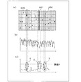
- FIG. 2 shows a series of processing results from scan image formation to pattern processing.
- FIG. 2A is a scanned image obtained by the above processing. Since a signal for detecting a line defect in the gate direction is used, this scanned image is referred to as a line defect enhancement pattern here.
- the line defect emphasis pattern the line defect 201 is thin, and the point defect 202 or other noise appears darker than the line defect. This is because line defects are often short-circuited and are not completely disconnected. Further, the line defect 201 appears in a band shape, and the point defect 202 or other noise appears in a dot shape. This is because the point defect 202 often occurs independently, whereas a plurality of line defects 201 often occur together.
- point defects occur in half picture elements, whereas line defects occur in one picture element.
- a projection process is performed on the line defect emphasis pattern (step S104). Specifically, the scanned image is scanned vertically and the average intensity of each projection line is obtained.
- FIG. 2B shows a projection waveform after the projection processing.
- difference processing is performed on the projection waveform (step S105). Generally, it is compared with the average value of adjacent picture elements, etc., but in the case of the present invention, there may be a case where it extends over a plurality of picture elements like a line defect. The region where the difference is larger than a predetermined numerical value is extracted as an object.
- FIG. 2C shows the waveform extracted using the difference processing.
- the respective peaks are substantially the same. This is because the defect strength of the line defect 201 is weak, but the corresponding portion X has a large number of pixels (wide), whereas the defect strength of the point defect 202 or other noise is strong, but the corresponding portion Y In the line defect emphasizing pattern, a large amount of point defects 202 or other noises are generated and the number of pixels of the line defect 201 having a weak defect intensity is integrated.
- the peak of the integrated value of the point defect 201 having a high value and the defect strength or the number of other noise pixels is the same, or in some cases, the peak may be high even in a portion other than the line defect 201. For this reason, even if the threshold value is set as the 0th threshold value in FIG. 2C, it is difficult to detect the line defect 201 depending on whether or not the 0th threshold value is exceeded.
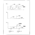
- FIG. 3 shows a process for detecting the line defect 201 based on the difference processed data.
- a first threshold is set for the waveform after difference processing (step S106).
- the first threshold value is set to be surely smaller than the peak of the waveform after the difference processing.
- FIG. 3A shows a state in which the first threshold is set.
- a specific threshold may be set based on past defect inspection data.
- the sum of the portions 301, 302, and 303 exceeding the first threshold is calculated for the waveform after the difference processing (step S107).
- FIG. 3B is a graph of the calculation result of step S107.
- a second threshold value is set for the graph of the calculation result (step S108).
- the second threshold is a threshold for discriminating whether the defect is a line defect or not, and may be set as appropriate based on past defect inspection data.
- FIG. 3C shows a state in which the second threshold is set. It is compared with this threshold value to determine whether or not the defect is a line defect (step S109). According to FIG.3 (c), the thing 302 exceeding the 2nd threshold value is determined to be a line defect (step S110), and the things 301 and 303 below the 2nd threshold value are determined to be a point defect or noise (step S111).
- Embodiment 2 will be described.
- line defects in the source direction were detected.
- the point that a normal inspection signal is applied to the TFT array substrate 2 is different from that in the second embodiment.
- a scanning image is obtained by detecting the surface potential distribution of the TFT array obtained by this inspection signal, and the obtained scanning image is subjected to projection processing and differential processing to obtain a defect detection waveform.
- a first threshold value is set for the waveform, and a sum is calculated for each portion exceeding the first threshold value.
- a second threshold value is set for the calculation result, and a value exceeding the second threshold value is determined as a line defect.
- Each specific threshold value may be set based on past defect inspection data. Since the defect intensity and the defect waveform are different in the source direction and the gate direction, it is possible to appropriately detect the line defects in the source direction and the gate direction by setting appropriate threshold values.
- FIG. 4 is a diagram for explaining a configuration example of the line defect detection device 1 of the present invention.
- the line defect detection device 1 includes an inspection signal forming unit 3 that applies an inspection signal to the TFT array substrate 2 to be inspected, an irradiation device 4 that irradiates the TFT array substrate with an electron beam, and a secondary electron that detects secondary electrons on the TFT substrate.
- a characteristic calculation unit 9 that calculates characteristics of the processed data and a detection unit 10 that detects line defects are provided.
- the TFT substrate 2 is a TFT substrate provided with pixel electrodes arranged in an array, a driving circuit for the TFT substrate, and wiring including a power supply line.
- the inspection signal forming unit 3 applies an inspection signal having a predetermined pattern corresponding to the defect inspection item.
- the irradiation device 4 arranges an electron beam source that irradiates the electron beam on the TFT substrate 2.
- the secondary electron detector 5 detects secondary electrons emitted from the TFT substrate 2 by the irradiated electron beam.
- the image forming unit 6 forms a scanned image based on the detected potential state of the secondary electrons.
- the projection processing unit 7 integrates pixel values of each pixel in one direction to which the TFT array is connected from the scanned image.
- the difference processing unit 8 sets a background image of the projection waveform as a reference image in advance for the projection processed data, performs subtraction for each pixel with the current waveform image, and obtains an area where the difference is larger than a predetermined numerical value. Extract as an object.
- the characteristic calculation unit 9 sets a first threshold value for the difference-processed data, and calculates a characteristic of a portion exceeding the first threshold value.
- the detection unit 10 sets a second threshold value for the calculated characteristic data, and detects a line defect based on the second threshold value.
- the sum of the portions exceeding the first threshold is calculated for the waveform after the difference processing.
- the method for determining the characteristics of the portion exceeding the first threshold is not limited to this. For example, a method of calculating a mountain-shaped area of a portion exceeding the first threshold or a full width at half maximum may be used.
- the line defect of the TFT array substrate can be extracted accurately and easily.
- the line defect detection method forms a scanning image of a surface potential by irradiating an electron beam onto a TFT array substrate, and detects the line defect of the TFT array from the scanning image.
- a projection processing step for integrating pixel values a difference processing step for obtaining data by performing difference processing on the projection processed data, a first threshold value is set for the data subjected to the difference processing, and the first A characteristic calculation step for calculating a characteristic value of a portion exceeding the threshold value, and a line defect detection process for setting a second threshold value for the characteristic value and detecting a line defect based on the second threshold value Characterized in that it comprises a.
- one form of the line defect detection method according to the present invention is characterized in that the characteristic calculation step calculates a sum of portions exceeding the first threshold.
- one form of the line defect detection method according to the present invention is characterized in that the characteristic calculation step calculates a full width at half maximum of a portion exceeding the first threshold.
- one form of the line defect detection method according to the present invention is characterized in that the line defect detection method detects a line defect in the gate direction of the TFT array substrate.
- one form of the line defect detection method according to the present invention is characterized in that the first threshold value and / or the second threshold value are made different depending on a gate or a source.
- the line defect detection device irradiates the electron beam onto the TFT array substrate to form a surface potential scan image, and detects a TFT array line defect from the scan image.
- a line defect detection device an image forming unit for forming a scanning image of a surface potential of a TFT array substrate obtained by irradiating an electron beam to the TFT array substrate, and a direction in which the TFT array is connected from the scanning image
- a projection processing unit that integrates pixel values of the respective pixels, a difference processing unit that performs difference processing on the projection-processed data and obtains data, and a first threshold is set for the difference-processed data.
- a characteristic calculator that calculates a characteristic value of a portion that exceeds the first threshold; and a detection that sets a second threshold for the characteristic value and detects a line defect based on the second threshold Characterized in that it comprises a.
- the line defect detection method and line defect detection apparatus according to the present invention can be suitably used for defect inspection of a TFT array substrate, for example.
Landscapes
- Engineering & Computer Science (AREA)
- Physics & Mathematics (AREA)
- Computer Hardware Design (AREA)
- General Physics & Mathematics (AREA)
- Theoretical Computer Science (AREA)
- Analysing Materials By The Use Of Radiation (AREA)
- Testing Electric Properties And Detecting Electric Faults (AREA)
Abstract
電子ビームをTFTアレイ基板上に照射して、表面電位の走査画像を形成し、前記走査画像からTFTアレイの線欠陥を検出する線欠陥検出方法であって、TFTアレイ基板に電子ビームを照射することにより得られるTFTアレイ基板の表面電位の走査画像を形成する工程と、前記走査画像からTFTアレイが接続された一方向の各画素の画素値を積算する投影処理工程と、前記投影処理されたデータについて、差分処理を行いデータを取得する差分処理工程と、前記差分処理されたデータについて、第1の閾値を設定し、前記第1の閾値を超えた部分の特性値を算出する特性算出工程と、前記特性値について、第2の閾値を設定し、前記第2の閾値に基づいて線欠陥を検出する線欠陥検出工程を含むことを特徴とする。
Description
本発明は、液晶ディスプレイや有機ELディスプレイなどに使われるTFT(Thin film transistor)アレイ基板の欠陥状況を検出する検査方法および検査装置に関する。
液晶基板や有機EL基板等のTFTアレイが形成された半導体基板の製造過程では、製造過程中にTFTアレイ検査工程を含み、このTFTアレイ検査工程において、TFTアレイの欠陥検査が行われている。TFTアレイ基板は、例えば、走査線として機能する複数本のゲート線が平行に配設されるとともに、信号線として機能する複数本のソース線がゲート線に直交して配設され、この両線が交差する部分の近傍にTFTが配設され、このTFTに画素電極(ピクセル)が接続される。
TFTアレイ検査装置としては、電子線方式や光学方式が知られており、電子線や光をTFTアレイ基板に照射することにより得られるTFTアレイ基板の電位状態を測定し、TFTアレイ基板の異常電位のピクセルを検出することによってTFTアレイの欠陥を検出する。
例えば、特許文献1には、TFTアレイ基板の各画素を駆動して得られる二次元の測定データについて、x方向及び/またはy方向の各ラインの測定データの積算値または平均強度を求めて同方向の累積プロファイルデータを作成し、作成した累積プロファイルデータから各ラインのしきい値を求め、各ラインの累積プロファイルデータと、この閾値を比較することで、TFTアレイ基板のx方向及び/またはy方向のラインについてライン単位で画素欠陥を検出するTFTアレイ検査方法が開示されている。図5は、該特許文献に示された検査方法を用いて、欠陥検出を行った結果を示したものである。TFTアレイ基板のソース方向においては、液晶に信号電圧がかかるため、点欠陥、線欠陥のいずれにおいてもその欠陥強度が強く、感度の低い信号を用いて測定されたデータであっても欠陥を検出しやすい。このため、単に測定データの積算値または平均値を求めて閾値と比較するだけで、その欠陥がどのような欠陥であるかを容易に判定することができる。たとえば、累積プロファイルデータの値が低ければ点欠陥、高ければ線欠陥、更に大幅に高ければ複数の線欠陥であると判定することができる。
しかしながら、上記特許文献に示された方法で実際にTFTアレイ基板のゲート方向の欠陥を検出する場合、ゲート方向の線欠陥を検出するために感度の高い信号を用いて測定を行うと、点欠陥の強度が大きく出てしまったり、信号の影響により発生したノイズも検出されてしまい、単純に積算値あるいは平均強度を求めて、閾値と比較するという方法では、それが点欠陥か、線欠陥か、あるいはその他のノイズであるかを明確に区別することができない。このような理由により、これまではゲート方向の線欠陥を検出する有効な方法は実用化されていなかった。
本発明は、上記の問題点に鑑みてなされたものであり、その目的は、TFTアレイ基板の欠陥検出において、ゲート方向の線欠陥でも明確に検出することができる線欠陥検出方法及び線欠陥検出装置を提供することにある。
本発明に係る線欠陥検出方法は、電子ビームをTFTアレイ基板上に照射して、表面電位の走査画像を形成し、前記走査画像からTFTアレイの線欠陥を検出する線欠陥検出方法であって、TFTアレイ基板に電子ビームを照射することにより得られるTFTアレイ基板の表面電位の走査画像を形成する工程と、前記走査画像からTFTアレイが接続された一方向の各画素の画素値を積算する投影処理工程と、前記投影処理されたデータについて、差分処理を行いデータを取得する差分処理工程と、前記差分処理されたデータについて、第1の閾値を設定し、前記第1の閾値を超えた部分の特性値を算出する特性算出工程と、前記特性値について、第2の閾値を設定し、前記第2の閾値に基づき線欠陥を検出する線欠陥検出工程を含むことを特徴とする。
また本発明に係る線欠陥検出装置は、電子ビームをTFTアレイ基板上に照射して、表面電位の走査画像を形成し、前記走査画像からTFTアレイの線欠陥を検出する線欠陥検出装置であって、TFTアレイ基板に電子ビームを照射することにより得られるTFTアレイ基板の表面電位の走査画像を形成する画像形成部と、前記走査画像からTFTアレイが接続された一方向の各画素の画素値を積算する投影処理部と、前記投影処理されたデータについて、差分処理を行いデータを取得する差分処理部と、前記差分処理されたデータについて、第1の閾値を設定し、前記第1の閾値を超えた部分の特性値を算出する特性算出部と、前記特性値について、第2の閾値を設定し、前記第2の閾値に基づき線欠陥を検出する検出部を備えることを特徴とする。
本発明によれば、TFTアレイ基板の欠陥検出において、ゲート方向の線欠陥でもノイズ等の影響を受けることなく、明確に検出することが可能となる。
以下、本発明の実施の形態について図を参照しながら以下に説明する。なお、本発明の図面において、同一の参照符号は、同一部分または相当部分を表わすものとする。
<実施形態1>
図1は、実施形態1の線欠陥検出の処理の流れを示したフローチャートである。なお、図中のSは、フローチャートにおける各ステップを表す。
図1は、実施形態1の線欠陥検出の処理の流れを示したフローチャートである。なお、図中のSは、フローチャートにおける各ステップを表す。
まず、TFTアレイに検査信号を印加し、この検査信号で得られるTFTアレイの表面電位分布を検出することで走査画像を取得する。本実施形態では、ゲート方向の線欠陥を検出するために感度の高い検査信号を用いる。TFTアレイ基板に検査信号を印加するとTFTアレイにはこの印加した検査信号に基づいて二次元的パターンの表面電位分布が形成される。このTFTアレイに電子ビームを照射し(ステップS101)、二次電子を検出する(ステップS102)。次に、検出された二次電子により得られるデータに基づいて走査画像を形成する(ステップS103)。
図2は、走査画像の形成からパターン処理までの一連の処理結果を示している。図2(a)は、上記の処理により得られた走査画像である。ゲート方向における線欠陥を検出するための信号を用いているので、ここでは、この走査画像を線欠陥強調パターンと呼ぶ。線欠陥強調パターンにおいては、線欠陥201は薄く、また、点欠陥202もしくはその他のノイズは線欠陥より濃く現れる。これは、線欠陥の場合はショートである場合が多く、完全に断線しているわけではないためである。また、線欠陥201は帯状に、また点欠陥202もしくはその他のノイズは、点状に現れる。これは、点欠陥202は単独で発生することが多いことに対し、線欠陥201は複数本まとまって発生することが多いためである。また、ゲート方向の両側にTFTが配置されたマルチドメインの構成である場合は、点欠陥は半絵素で発生するのに対し、線欠陥では1絵素で発生するためである。
次に、線欠陥強調パターンに対して投影処理を行う(ステップS104)。具体的には、走査画像に対して、垂直にスキャンを行い、各投影ラインの平均強度を求める。図2(b)は、投影処理を行った投影波形である。次に、上記投影波形に対して差分処理を行う(ステップS105)。一般的には、隣接する絵素の平均値等と比較するが、本発明の場合は、線欠陥のように複数の絵素にまたがる場合があるので、複数絵素離れた絵素との比較を行い、差分が所定の数値よりも大きくなる領域を対象物として抽出する。図2(c)は、差分処理を用いて波形の抜き出しを行ったものである。
ここで、差分処理を行った波形において、線欠陥201に対応する部分Xと、点欠陥202、もしくはその他のノイズに対応する部分Yを比較すると、それぞれのピークはほぼ同じである。これは、線欠陥201の欠陥強度は弱いが、対応する部分Xの画素数は多い(幅が広い)のに対し、点欠陥202、もしくはその他のノイズの欠陥強度は強いが、対応する部分Yの画素数は少ない(幅が狭い)ことに起因しており、線欠陥強調パターンにおいては、点欠陥202、もしくはその他のノイズが大量に発生し、欠陥強度の弱い線欠陥201の画素数の積算値と欠陥強度の強い点欠陥201もしくはその他のノイズの画素数の積算値のピークが同じ、あるいは場合によっては、線欠陥201以外の部分でもピークが高く出てしまうことがあるためである。このため、閾値を仮に第0の閾値として図2(c)に設定しても、第0の閾値を超えるか否かによって、線欠陥201を検出することは困難である。
図3は、差分処理したデータに基づき、線欠陥201を検出する処理を示したものである。まず、差分処理後の波形に対し第1の閾値を設定する(ステップS106)。第1の閾値は、差分処理後の波形のピークよりも必ず小さくなるように設定する。図3(a)は、第1の閾値を設定した状態を示している。具体的な閾値は、過去の欠陥検査データに基づき、設定すればよい。次に、差分処理後の波形に対し、第1の閾値を越えた部分301、302、303の和をそれぞれ算出する(ステップS107)。図3(b)は、ステップS107の算出結果をグラフ化したものである。次にこの算出結果のグラフに対し、第2の閾値を設定する(ステップS108)。第2の閾値は、その欠陥が、線欠陥であるか、それ以外かを区別する閾値であり、過去の欠陥検査データに基づき、適宜設定すればよい。図3(c)は第2の閾値を設定した状態を示している。この閾値と比較して、欠陥が線欠陥か否かを判定する(ステップS109)。図3(c)によれば、第2の閾値を超えたもの302が線欠陥(ステップS110)、第2の閾値以下のもの301、303が点欠陥もしくはノイズと判定される(ステップS111)。
<実施形態2>
次に、実施形態2について説明する。上記と同様にしてソース方向の線欠陥検出を行った。ソース方向の場合は、上述したように欠陥強度が強いため、TFTアレイ基板2に通常の検査信号を印加する点が実施形態2とは異なる。この検査信号で得られるTFTアレイの表面電位分布を検出することで走査画像を取得し、得られた走査画像に対して、投影処理、差分処理を行い、欠陥検出の波形を得る。
次に、実施形態2について説明する。上記と同様にしてソース方向の線欠陥検出を行った。ソース方向の場合は、上述したように欠陥強度が強いため、TFTアレイ基板2に通常の検査信号を印加する点が実施形態2とは異なる。この検査信号で得られるTFTアレイの表面電位分布を検出することで走査画像を取得し、得られた走査画像に対して、投影処理、差分処理を行い、欠陥検出の波形を得る。
ここで、上記波形に対し第1の閾値を設定し、第1の閾値を越えた部分についてそれぞれの和を算出する。次にこの算出結果に対して第2の閾値を設定し、第2の閾値を超えたものを線欠陥と判定する。それぞれの具体的な閾値は、過去の欠陥検査データに基づき、設定すればよい。ソース方向、ゲート方向においては、欠陥強度や欠陥波形が異なるため、それぞれに適した閾値を設定することでソース方向、ゲート方向の線欠陥を適切に検出することが可能となる。
図4は、本発明の線欠陥検出装置1の一構成例を説明するための図である。線欠陥検出装置1は、検査対象であるTFTアレイ基板2に検査信号を印加する検査信号形成部3、TFTアレイ基板に電子ビームを照射する照射装置4、TFT基板の二次電子を検出する二次電子検出部5と、走査画像を形成する画像形成部6と、走査画像から画素値を積算する投影処理部7と、投影処理されたデータについて、差分処理を行う差分処理部8と、差分処理されたデータについて特性を算出する特性算出部9と、線欠陥を検出する検出部10とを備える。
TFT基板2は、アレイ状に配置されたピクセル電極と、TFT基板の駆動回路と、電源ラインを含む配線とを備えるTFT基板である。検査信号形成部3は、欠陥検査項目に応じた所定パターンの検査信号を印加する。照射装置4は、例えば荷電粒子ビームとして電子線を用いる場合には、TFT基板2上に電子線を照射する電子線源を配置する。二次電子検出部5は、照射された電子線によってTFT基板2から放出される二次電子を検出する。画像形成部6は、検出された二次電子の電位状態に基づき走査画像を形成する。投影処理部7は、走査画像からTFTアレイが接続された一方向の各画素の画素値を積算する。差分処理部8は、投影処理されたデータについて投影波形の背景画像をあらかじめ基準画像とし、現在の波形画像との間で画素ごとの引き算を行い、その差分が所定の数値よりも大きくなる領域を対象物として抽出する。特性算出部9は、差分処理されたデータについて、第1の閾値を設定し、前記第1の閾値を超えた部分の特性を算出する。検出部10は、算出された特性データについて第2の閾値を設定し、前記第2の閾値に基づいて線欠陥を検出する。
なお、本実施の形態では、差分処理後の波形に対し、第1の閾値を越えた部分の和を算出したが、第1の閾値を越えた部分の特性を決定する方法はこれに限らず、例えば、第1の閾値を越えた部分の山形の面積、あるいは全半値幅を算出する方法などを用いても構わない。
以上説明したように、本発明の線欠陥抽出方法を用いることで、TFTアレイ基板の線欠陥の抽出を正確かつ容易に行うことができる。
なお、本発明は上述した各実施形態に限定されるものではない。当業者は、請求項に示した範囲内において、本発明をいろいろと変更できる。すなわち、請求項に示した範囲内において、適宜変更された技術的手段を組み合わせれば、新たな実施形態が得られる。すなわち、発明の詳細な説明の項においてなされた具体的な実施形態は、あくまでも、本発明の技術内容を明らかにするものであって、そのような具体例にのみ限定して狭義に解釈されるべきものではなく、本発明の精神と次に記載する請求の範囲内で、いろいろと変更して実施することができるものである。
(本発明の総括)
以上のように、本発明に係る線欠陥検出方法は、電子ビームをTFTアレイ基板上に照射して、表面電位の走査画像を形成し、前記走査画像からTFTアレイの線欠陥を検出する線欠陥検出方法であって、TFTアレイ基板に電子ビームを照射することにより得られるTFTアレイ基板の表面電位の走査画像を形成する工程と、前記走査画像からTFTアレイが接続された一方向の各画素の画素値を積算する投影処理工程と、前記投影処理されたデータについて、差分処理を行いデータを取得する差分処理工程と、前記差分処理されたデータについて、第1の閾値を設定し、前記第1の閾値を超えた部分の特性値を算出する特性算出工程と、前記特性値について、第2の閾値を設定し、前記第2の閾値に基づき線欠陥を検出する線欠陥検出工程を含むことを特徴とする。
以上のように、本発明に係る線欠陥検出方法は、電子ビームをTFTアレイ基板上に照射して、表面電位の走査画像を形成し、前記走査画像からTFTアレイの線欠陥を検出する線欠陥検出方法であって、TFTアレイ基板に電子ビームを照射することにより得られるTFTアレイ基板の表面電位の走査画像を形成する工程と、前記走査画像からTFTアレイが接続された一方向の各画素の画素値を積算する投影処理工程と、前記投影処理されたデータについて、差分処理を行いデータを取得する差分処理工程と、前記差分処理されたデータについて、第1の閾値を設定し、前記第1の閾値を超えた部分の特性値を算出する特性算出工程と、前記特性値について、第2の閾値を設定し、前記第2の閾値に基づき線欠陥を検出する線欠陥検出工程を含むことを特徴とする。
また、本発明に係る線欠陥検出方法の一形態は、前記特性算出工程は、前記第1の閾値を越えた部分の和を算出することを特徴とする。
また、本発明に係る線欠陥検出方法の一形態は、前記特性算出工程は、前記第1の閾値を越えた部分の全半値幅を算出することを特徴とする。
また、本発明に係る線欠陥検出方法の一形態は、前記線欠陥検出方法は、前記TFTアレイ基板のゲート方向の線欠陥を検出することを特徴とする。
また、本発明に係る線欠陥検出方法の一形態は、ゲートまたはソースに応じて、前記第1の閾値及び/または第2の閾値を異ならせることを特徴とする。
また、本発明に係る線欠陥検出装置は、以上のように、電子ビームをTFTアレイ基板上に照射して、表面電位の走査画像を形成し、前記走査画像からTFTアレイの線欠陥を検出する線欠陥検出装置であって、TFTアレイ基板に電子ビームを照射することにより得られるTFTアレイ基板の表面電位の走査画像を形成する画像形成部と、前記走査画像からTFTアレイが接続された一方向の各画素の画素値を積算する投影処理部と、前記投影処理されたデータについて、差分処理を行いデータを取得する差分処理部と、前記差分処理されたデータについて、第1の閾値を設定し、前記第1の閾値を超えた部分の特性値を算出する特性算出部と、前記特性値について、第2の閾値を設定し、前記第2の閾値に基づき線欠陥を検出する検出部を備えることを特徴とする。
本発明に係る線欠陥検出方法及び線欠陥検出装置は、例えばTFTアレイ基板の欠陥検査に好適に利用できる。
1 線欠陥検出装置
2 TFTアレイ基板
3 検査信号形成部
4 照射装置
5 二次電子検出部
6 画像形成部
7 投影処理部
8 差分処理部
9 特性算出部
10 検出部
201 線欠陥
202 点欠陥
2 TFTアレイ基板
3 検査信号形成部
4 照射装置
5 二次電子検出部
6 画像形成部
7 投影処理部
8 差分処理部
9 特性算出部
10 検出部
201 線欠陥
202 点欠陥
Claims (6)
- 電子ビームをTFTアレイ基板上に照射して、表面電位の走査画像を形成し、前記走査画像からTFTアレイの線欠陥を検出する線欠陥検出方法であって、
TFTアレイ基板に電子ビームを照射することにより得られるTFTアレイ基板の表面電位の走査画像を形成する工程と、
前記走査画像からTFTアレイが接続された一方向の各画素の画素値を積算する投影処理工程と、
前記投影処理されたデータについて、差分処理を行いデータを取得する差分処理工程と、
前記差分処理されたデータについて、第1の閾値を設定し、前記第1の閾値を超えた部分の特性値を算出する特性算出工程と、
前記特性値について、第2の閾値を設定し、前記第2の閾値に基づき線欠陥を検出する線欠陥検出工程を含むことを特徴とする線欠陥検出方法。 - 前記特性算出工程は、前記第1の閾値を越えた部分の和を算出することを特徴とする請求項1に記載の線欠陥検出方法。
- 前記特性算出工程は、前記第1の閾値を越えた部分の全半値幅を算出することを特徴とする請求項1に記載の線欠陥検出方法。
- 前記線欠陥検出方法は、前記TFTアレイ基板のゲート方向の線欠陥を検出することを特徴とする請求項1から3のいずれかに記載の線欠陥検出方法。
- 前記線欠陥検出方法は、ゲートまたはソースに応じて、前記第1の閾値及び/または第2の閾値を異ならせることを特徴とする請求項1から3のいずれかに記載の線欠陥検出方法。
- 電子ビームをTFTアレイ基板上に照射して、表面電位の走査画像を形成し、前記走査画像からTFTアレイの線欠陥を検出する線欠陥検出装置であって、
TFTアレイ基板に電子ビームを照射することにより得られるTFTアレイ基板の表面電位の走査画像を形成する画像形成部と、
前記走査画像からTFTアレイが接続された一方向の各画素の画素値を積算する投影処理部と、
前記投影処理されたデータについて、差分処理を行いデータを取得する差分処理部と、
前記差分処理されたデータについて、第1の閾値を設定し、前記第1の閾値を超えた部分の特性値を算出する特性算出部と、
前記特性値について、第2の閾値を設定し、前記第2の閾値に基づき線欠陥を検出する検出部を備えることを特徴とする線欠陥検出装置。
Applications Claiming Priority (2)
| Application Number | Priority Date | Filing Date | Title |
|---|---|---|---|
| JP2011033030A JP5015334B1 (ja) | 2011-02-18 | 2011-02-18 | 線欠陥検出方法及び線欠陥検出装置 |
| JP2011-033030 | 2011-02-18 |
Publications (1)
| Publication Number | Publication Date |
|---|---|
| WO2012111841A1 true WO2012111841A1 (ja) | 2012-08-23 |
Family
ID=46672748
Family Applications (1)
| Application Number | Title | Priority Date | Filing Date |
|---|---|---|---|
| PCT/JP2012/053993 Ceased WO2012111841A1 (ja) | 2011-02-18 | 2012-02-20 | 線欠陥検出方法及び線欠陥検出装置 |
Country Status (2)
| Country | Link |
|---|---|
| JP (1) | JP5015334B1 (ja) |
| WO (1) | WO2012111841A1 (ja) |
Citations (2)
| Publication number | Priority date | Publication date | Assignee | Title |
|---|---|---|---|---|
| JP2005208245A (ja) * | 2004-01-21 | 2005-08-04 | Shimadzu Corp | Tftアレイ検査方法及びtftアレイ検査装置 |
| JP2009079922A (ja) * | 2007-09-25 | 2009-04-16 | Shimadzu Corp | Tftアレイの検査方法及びtftアレイ検査装置 |
-
2011
- 2011-02-18 JP JP2011033030A patent/JP5015334B1/ja not_active Expired - Fee Related
-
2012
- 2012-02-20 WO PCT/JP2012/053993 patent/WO2012111841A1/ja not_active Ceased
Patent Citations (2)
| Publication number | Priority date | Publication date | Assignee | Title |
|---|---|---|---|---|
| JP2005208245A (ja) * | 2004-01-21 | 2005-08-04 | Shimadzu Corp | Tftアレイ検査方法及びtftアレイ検査装置 |
| JP2009079922A (ja) * | 2007-09-25 | 2009-04-16 | Shimadzu Corp | Tftアレイの検査方法及びtftアレイ検査装置 |
Also Published As
| Publication number | Publication date |
|---|---|
| JP2012173034A (ja) | 2012-09-10 |
| JP5015334B1 (ja) | 2012-08-29 |
Similar Documents
| Publication | Publication Date | Title |
|---|---|---|
| CN104160439B (zh) | 显示设备的显示不均匀检测方法以及其装置 | |
| CN104137171B (zh) | 显示设备的显示不均匀检测方法及其装置 | |
| US7952699B2 (en) | Apparatus of inspecting defect in semiconductor and method of the same | |
| JP5787746B2 (ja) | 信号処理方法および信号処理装置 | |
| US8712184B1 (en) | Method and system for filtering noises in an image scanned by charged particles | |
| JP5459973B2 (ja) | 試料検査装置 | |
| JP2014035326A (ja) | 欠陥検査装置 | |
| IL281347B1 (en) | Detecting defects in a logic region on a wafer | |
| JP2010287442A (ja) | 電池の検査方法及び電池の検査装置 | |
| WO2010004914A1 (ja) | 致命傷の検出方法 | |
| JP5459469B2 (ja) | Tftアレイの検査方法、およびtftアレイの検査装置 | |
| JP2011053044A (ja) | メッシュ検査装置、メッシュ検査方法、プログラム、および記録媒体 | |
| JP5015334B1 (ja) | 線欠陥検出方法及び線欠陥検出装置 | |
| JP2008071988A (ja) | 半導体装置の欠陥検査装置及び欠陥検査方法 | |
| JP6119784B2 (ja) | 異物検査方法 | |
| JP2005321308A (ja) | アレイ検査装置 | |
| JP4386175B2 (ja) | Tftアレイ検査方法 | |
| JP5182595B2 (ja) | Tftアレイ検査方法およびtftアレイ検査装置 | |
| US20120262612A1 (en) | Electro optical modulator, electro optical sensor, and detecting method thereof | |
| JP5236615B2 (ja) | エッジ部分検出方法、測長方法、荷電粒子線装置 | |
| JP6729526B2 (ja) | 欠陥サイズ分布の測定方法 | |
| US20140061461A1 (en) | Defect inspection apparatus, defect inspection method and non-transitory computer readable recording medium | |
| JP2010135679A (ja) | 半導体検査装置及び検査方法 | |
| Kramer et al. | Physical matching of CD-SEM: noise analysis and verification in FAB environment | |
| KR20140068557A (ko) | 결함 검사 장치 및 이를 이용한 표시장치의 결함 검사 방법 |
Legal Events
| Date | Code | Title | Description |
|---|---|---|---|
| 121 | Ep: the epo has been informed by wipo that ep was designated in this application |
Ref document number: 12746696 Country of ref document: EP Kind code of ref document: A1 |
|
| NENP | Non-entry into the national phase |
Ref country code: DE |
|
| 122 | Ep: pct application non-entry in european phase |
Ref document number: 12746696 Country of ref document: EP Kind code of ref document: A1 |