WO2012111604A1 - 線幅測定装置 - Google Patents
線幅測定装置 Download PDFInfo
- Publication number
- WO2012111604A1 WO2012111604A1 PCT/JP2012/053252 JP2012053252W WO2012111604A1 WO 2012111604 A1 WO2012111604 A1 WO 2012111604A1 JP 2012053252 W JP2012053252 W JP 2012053252W WO 2012111604 A1 WO2012111604 A1 WO 2012111604A1
- Authority
- WO
- WIPO (PCT)
- Prior art keywords
- camera
- pattern
- line width
- magnification
- substrate
- Prior art date
- Legal status (The legal status is an assumption and is not a legal conclusion. Google has not performed a legal analysis and makes no representation as to the accuracy of the status listed.)
- Ceased
Links
Images



Classifications
-
- G—PHYSICS
- G01—MEASURING; TESTING
- G01B—MEASURING LENGTH, THICKNESS OR SIMILAR LINEAR DIMENSIONS; MEASURING ANGLES; MEASURING AREAS; MEASURING IRREGULARITIES OF SURFACES OR CONTOURS
- G01B11/00—Measuring arrangements characterised by the use of optical techniques
- G01B11/02—Measuring arrangements characterised by the use of optical techniques for measuring length, width or thickness
Definitions
- the present invention relates to a line width measuring apparatus.
- the present invention relates to a line width measuring device for measuring a pattern line width or interval formed on a large glass substrate. Note that this application claims priority based on Japanese Patent Application No. 2011-31563 filed on Feb. 17, 2011, the entire contents of which are incorporated herein by reference. .
- the line width measuring device or the dimension measuring device is a device for measuring the pattern line width or interval of a liquid crystal panel substrate (for example, a TFT substrate) or the pattern line width or interval of a mask for manufacturing a semiconductor device.
- the line width measuring apparatus for example, enlarges a pattern image obtained by irradiating a film pattern formed on a transparent glass substrate with a microscope, and then displays the image with an image sensor (for example, a CCD). The size or shape is measured by performing image processing on a pattern image obtained by imaging with a camera.
- the line width measuring device, the dimension measuring device, the line width inspecting device, or the dimension inspecting device is referred to as a “line width measuring device”.
- a liquid crystal panel which is a component of a liquid crystal display device (LCD) has a structure in which a pair of glass substrates are opposed to each other with a predetermined gap secured.
- glass substrates (mother glass) for liquid crystal panels are becoming larger year by year.
- the mother glass has a side exceeding 1 m (for example, from 1100 mm ⁇ 1300 mm (fifth generation substrate) to 2880 mm ⁇ 3130 mm (tenth generation substrate)).
- the mother glass has a side exceeding 1 m (for example, from 1100 mm ⁇ 1300 mm (fifth generation substrate) to 2880 mm ⁇ 3130 mm (tenth generation substrate)).
- a plurality of film patterns to be inspected having the same shape are present on the mother glass of the object to be measured.
- the exposure error (positional deviation) of the film pattern formed on the object to be measured tends to generally increase accordingly.
- the line width measuring apparatus does not move on the object even if the XY stage is moved to image a predetermined measurement position. Since the pattern position is shifted, a part of the measurement target area that is necessary in the captured image may protrude (for example, Patent Document 2).
- an object to be measured is carried on a sample table by a transfer robot or the like, and positioning stoppers such as fixing pins are provided on the sample table in the X and Y directions, respectively. Then, once the sample is placed on the sample table, the object to be measured is pressed against the stopper in the X and Y directions to improve the positioning accuracy. Thereafter, for example, the object to be measured is adsorbed by an adsorbing mechanism, and the object to be measured is fixed to the sample stage.
- the position of the object to be measured is similar to the above.
- a positioning mechanism is provided to reduce the deviation.
- the object to be measured is positioned by the positioning mechanism at the time of loading by a transport robot or the like so as not to impair the accuracy and sequence of measurement.
- the object to be measured becomes larger, it becomes difficult to move the object itself due to the influence of its mass, static electricity, etc., compulsory positioning becomes difficult, and a lot of positioning operation failures occur. It has become like this. Therefore, it is also proposed to perform alignment correction processing by moving the position of the imaging head unit instead of the positioning operation at the time of carrying in (for example, Patent Document 1).
- FIG. 1 is a block diagram showing a schematic configuration of a line width measuring apparatus 500 disclosed in Patent Document 1.
- the line width measuring apparatus 500 illustrated in FIG. 1 includes a measuring unit 501.
- the measurement unit 501 includes an imaging head unit 508, a sample stage 509, a position correction unit 510, an air vibration isolation table 512, an illumination power source 513, a stage control unit 520, a transmission illumination power source 521, and a transmission illumination head unit 522.
- the imaging head unit 508 includes an observation color camera unit, a measurement camera unit, an electric revolver unit, a laser autofocus unit, and the like.
- the line width measuring apparatus 501 is provided with a color monitor 514, a measurement monitor 515, and a measurement result display monitor 516. Further, the line width measuring apparatus 501 is provided with a video printer 517, an image processing PC (Personal Computer) 518, and a control PC 519.
- PC Personal Computer
- the line width measuring apparatus 500 an image taken by the observation color camera of the imaging head unit 508 is displayed on the color monitor 514, and an image taken by the measurement camera is displayed on the measurement monitor 515.
- the line width measuring apparatus 500 starts measurement in response to an instruction from the external host (HOST) or the control PC 519.
- the measurement is started automatically or manually based on a preset recipe, and the measurement result is displayed on the measurement result display monitor 516.
- the measurement result is written in a predetermined area of a storage device such as an HD (Hard Disk) in the control PC 519, for example.
- the measurement result data is distributed to the external host in response to a request from the external host.
- the air vibration isolation table 512 prevents external vibration from being transmitted to the sample table 509.
- the image processing PC 518 analyzes the image input from the imaging head unit 508 and recognizes a predetermined pattern set in advance in the measurement object. Then, the position coordinates are acquired to obtain the correction amount. The obtained correction amount information is output to the control PC 519, and the control PC 519 outputs a control instruction signal to the stage control unit 520 based on the correction amount information.
- the stage control unit 520 performs position correction by giving a control signal corresponding to the input control instruction signal to the position correction unit 510. As described above, in the line width measuring apparatus 500 shown in FIG. 1, even when the mounting position of the object to be measured cannot be forcibly moved mechanically by the correction by the position correction unit 510, the positional deviation correction is performed. It can be performed.
- the positional deviation can be corrected by the correction by the position correction unit 510.
- the positional deviation correction at the time of carry-in is performed, there is a case in which the measured site does not fit in the camera only by moving the camera of the line width measuring device once. I understood it. This will be further described below.
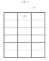
- FIG. 2 schematically shows the upper surface of the mother glass 110 on which the liquid crystal panel portion (115) having a predetermined dimension is multi-faced.
- the mother glass 110 shown in FIG. 2 is a 10th generation mother glass, and has a size of 2880 mm ⁇ 3130 mm, for example.
- each panel region 115 in the mother glass 110 corresponds to a 40-inch liquid crystal panel.
- TFT substrate the array substrate
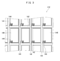
- a switching element (for example, TFT) 144 and a pixel electrode 146 are provided on the upper surface of the array substrate 112 (the surface of the array substrate 112 facing the liquid crystal layer, that is, the surface facing the color filter substrate). ing.
- a source wiring 141 and a gate wiring 142 are provided around the switching element 144 and the pixel electrode 146 so as to form a lattice pattern.
- the source wiring 141 and the gate wiring 142 are connected to the source electrode and the gate electrode of the switching element 144, respectively.
- the pixel electrode 146 is made of, for example, ITO (indium tin oxide).
- the pixel electrode 146 is formed in a rectangular shape, and in the example illustrated in FIG. 3, the pixel electrode 146 is formed in an elongated rectangular shape along the direction in which the source wiring 141 extends.
- the line width measuring device measures a part of the pattern shown in FIG. 3 (for example, the width of the source wiring 141, etc.), and determines the quality.
- a part of the pattern as shown in FIG. 3 (for example, the width of the source wiring 141) is enormous in the panel region 115 shown in FIG. 2, and the panel region 115 is formed on the mother glass 110.
- a plurality are arranged. Therefore, there are a large number of points to be measured by the line width measuring device (for example, about 350 points or more), and how to accurately and efficiently measure the points is a major theme. .
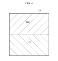
- the mother glass 110 shown in FIG. 4 is an array substrate 112 on which a pattern as shown in FIG. 3 is formed.
- One camera of the line width measuring device images the upper half area 111a of the mother glass 110, while the other camera of the line width measuring apparatus images the lower half area 111b of the mother glass 110.
- the camera inspection of the upper half area 111a it was possible to capture a normal image with almost one movement, but with the camera inspection of the lower half area 111b, almost all of the movement was performed with one movement. A case was observed where imaging could not be performed normally at the measurement point.
- the pattern of the measurement target is included in the camera position.
- the measurement target is located in the camera position. Does not contain patterns. Therefore, in the lower half area 111b, after the camera is moved once, the camera is moved to determine whether there is a measurement target pattern around it, and after the measurement target pattern is found, the measurement target pattern is measured. is necessary. Therefore, compared with the upper half area 111a, the measurement time of the lower half area 111b is very long, which naturally leads to a decrease in throughput.
- both of the two cameras are correcting the positional deviation of the loading position at the time of loading, there should be no problem of positional deviation of both cameras.
- one camera can capture and measure with a single movement, and the other camera cannot capture and measure with a single movement.
- the line width measuring device for measuring in such a state is left as it is, not only the measurement work efficiency is bad, but also a malfunction of the line width measurement may be missed.
- the present invention has been made in view of such a point, and a main object thereof is to provide a line width measuring apparatus capable of accurately and efficiently measuring an object to be measured.
- a line width measuring apparatus is a line width measuring apparatus that measures a line width of a pattern to be measured, a camera that images the pattern to be measured, a camera moving apparatus that moves the camera, and the camera movement And a control device that controls movement of the device, wherein the pattern to be measured is formed on a substrate for a liquid crystal panel that displays at least four primary colors, and the control device images the pattern imaged by the camera.
- An image analysis program to be analyzed is connected to a storage device, and the control device has a first camera magnification for measuring a line width of the pattern to be measured, and a magnification lower than the first camera magnification.
- a camera magnification switching device for switching between a second camera magnification for recognizing a pixel region included in the substrate
- the control device is configured to connect the second camera. After recognizing the picture element region by the camera with a magnification, and controls the camera so as to image the pattern of the measurement target by the camera with the first camera magnification.
- the apparatus further includes a stage on which the substrate is placed.
- the substrate is a mother glass for a liquid crystal panel displaying four primary colors, and the image data of the pattern to be measured is Registered in the storage device, and the control device has a function of collating the pattern of the measurement target imaged by the camera with the image data of the pattern of the measurement target registered in the storage device. ing.
- an alignment mark indicating a reference position is provided on the substrate on which the pattern to be measured is formed, and the image analysis program causes the camera to capture the alignment mark. Moving the camera moving device; moving the camera to first prescribed coordinates with reference to the alignment mark; and, at the first prescribed coordinates, moving the pixel region at the second camera magnification.
- a step of recognizing a step of switching from the second camera magnification to the first camera magnification; a step of searching for the same pattern as a registered pattern registered in the storage device at the first camera magnification; and Recognizing the pattern of the measurement object at the first specified coordinates; Measuring the identified line width of the pattern of the measurement target, from the first specified coordinates, and a step of moving said camera to said second specified coordinates.
- a color identification mark indicating a color in the four primary color display is formed on the substrate, and in the step of recognizing the pixel region, the camera images the color identification mark. Executed by.
- the image analysis program recognizes the pixel region at the second specified coordinate at the second camera magnification after moving the camera to the second specified coordinate.
- the image analysis program recognizes the pixel region at the second specified coordinate at the second camera magnification after moving the camera to the second specified coordinate.
- Switching from the second camera magnification to the first camera magnification searching for the same pattern as the registered pattern registered in the storage device at the first camera magnification, Recognizing the pattern of the measurement object at two specified coordinates; measuring the line width of the recognized pattern of the measurement object; from the second specified coordinates to the third specified coordinates; Moving the camera.
- the image analysis program executes the step of unloading the substrate after the step of measuring the line width of the pattern to be measured at all the specified coordinates is executed.
- the camera includes at least a first imaging unit and a second imaging unit.
- a line width measuring method is a line width measuring method for measuring a line width of a pattern to be measured, a step of carrying a substrate for a liquid crystal panel with a display of at least four primary colors onto a stage, and the substrate Obtaining the type and layer information, imaging the alignment mark formed on the substrate with a camera, and moving the camera to first prescribed coordinates with reference to the alignment mark; Recognizing the pixel region at the second camera magnification at the first specified coordinates, and switching from the second camera magnification to a first camera magnification having a higher magnification than the second camera magnification. Searching for the same pattern as the registered pattern registered in the storage device at the first camera magnification, and the first prescribed position by the search. Recognizing the pattern of the measurement object in step, measuring the line width of the recognized pattern of the measurement object, and moving the camera from the first prescribed coordinate to the second prescribed coordinate. Process.
- the line width measuring apparatus of the present invention after the pixel area is recognized by the camera having the second camera magnification for recognizing the pixel area, the first camera magnification for measuring the line width of the pattern to be measured is provided.
- the pattern to be measured is imaged with a camera. Therefore, it is possible to suppress the measurement of the pixel region of the adjacent color due to the camera shift.
- a line width measuring device that measures the line width of a pattern to be measured formed on a substrate for a liquid crystal panel by displaying at least four primary colors.
- FIG. 1 It is a figure which shows the structure of the conventional line
- (A) is a figure which shows the pattern of the area
- (b) is a figure which shows the pattern (45) of the registered measuring object. It is a top view which shows a mode that the color identification mark 47 is imaged in the pixel area
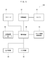
- FIG. 5 is a block diagram schematically showing the configuration of the line width measuring apparatus 100 according to the embodiment of the present invention.
- the line width measuring apparatus 100 of this embodiment is a line width measuring apparatus that measures the line width of a pattern to be measured, and is referred to as a dimension measuring apparatus, a line width inspecting apparatus, or a dimension inspecting apparatus in addition to the line width measuring apparatus. However, in this embodiment, it is referred to as a “line width measuring device”.
- the line width measuring apparatus 100 includes a camera 30 that captures a pattern to be measured, a camera moving device 32 that moves the camera 30, and a control device 40 that controls the movement of the camera moving device 32. Yes.
- the pattern to be measured in the present embodiment is formed on a substrate for a liquid crystal panel that displays at least four primary colors.
- control device 40 of the present embodiment is connected to a storage device 50 in which an image analysis program 52 for analyzing an image of a pattern captured by the camera 30 is stored.
- the image analysis program 52 is a program that can measure the line width (or interval) of the pattern from image data including the pattern captured by the camera 30.
- the camera 30 of this embodiment is, for example, a CCD image sensor or a CMOS image sensor.
- the camera moving device 32 of this embodiment is a mechanical device that can move the camera 30 in the XY directions.
- the control device 40 of the present embodiment is composed of a semiconductor integrated circuit, and is, for example, an MPU (micro processing unit) or a CPU (central processing unit).
- the storage device 50 of this embodiment is, for example, a hard disk (HDD), a semiconductor memory, an optical disk, a magneto-optical disk, or the like.
- the control device 40 is connected to an input device 62 (keyboard, mouse, touch panel, etc.) and an output device 64 (display, etc.).
- an input device 62 keyboard, mouse, touch panel, etc.
- an output device 64 display, etc.
- a general-purpose PC personal computer
- control device 40 of the present embodiment is connected to a camera magnification switching device 55 that switches between a first camera magnification (for example, 50 times) and a second camera magnification (for example, 20 times).
- the first camera magnification (for example, 50 times) is a magnification for measuring the line width of the pattern to be measured.
- the second camera magnification (for example, 20 times) is a magnification for recognizing the pixel region included in the substrate at a magnification lower than the first camera magnification (for example, 50 times).
- the camera magnification switching device 55 of the present embodiment is a device that enlarges / reduces image data captured by the camera 30, in other words, a program for changing the magnification of the image data captured by the camera 30. It is a device equipped.
- the program for constructing the camera magnification switching device 55 of this embodiment is stored in the same member as the storage device 50, and is stored in, for example, a hard disk (HDD), a semiconductor memory, or the like.
- the program for constructing the camera magnification switching device 55 may be stored in a part of the storage device 50 or may be stored in a device different from the storage device 50.
- the storage device 50 is a hard disk
- a program for constructing the camera magnification switching device 55 can be stored in a part of the hard disk.
- the camera magnification switching device 55 is not limited to a software device, and may be a device that optically changes the magnification of the camera 30.
- the control device 40 recognizes the pixel region with the camera 30 having the second camera magnification (for example, 20 times) and then uses the camera 30 with the first camera magnification (for example, 50 times).
- the camera 30 is controlled so as to capture the pattern to be measured. That is, the camera 30 once captures a wide area and identifies a target pixel region (for example, a green (G) pixel region), and then targets a pixel region (for example, a green (G) pixel).
- the pattern of the measurement target included in (region) is imaged.
- the target pixel region is recognized, and then the line width of the pattern to be measured in the target pixel region is determined. Can be measured. Therefore, in the line width measurement of a liquid crystal panel using a color filter composed of four primary colors of red (R), green (G), blue (B), and yellow (Y), even if a camera shift occurs, It is possible to avoid an erroneous measurement of measuring a color pixel region.
- the displacement of the camera 30 is not the displacement of the positioning that occurs when the substrate is carried onto the stage 20 but the data of the coordinate displacement that accompanies the movement of the camera 30.
- the cause of the occurrence of the coordinate shift accompanying the movement of the camera 30 is often not fully grasped even if it is specified in considerable detail. Therefore, when the coordinate shift occurs, the camera moving device 32 moves the camera 30 to a predetermined coordinate, so that the camera 30 captures the pattern to be measured in the target pixel area. In many cases, it is not possible to specify whether or not the pattern of the measurement target in the pixel area different from the target (for example, the adjacent pixel area) is captured.
- the size (area) of each pixel region is different. . Therefore, the same kind of measurement in the adjacent pixel region (for example, the blue (B) region) is caused by the movement shift in an attempt to capture the pattern of the measurement target in the narrow pixel region (for example, the green (G) region). There is a possibility that the target pattern is imaged, and it is difficult to notice the error.
- the size (area) of each pixel region is the same (or substantially the same).
- the line width measuring apparatus 100 measures line width in a liquid crystal panel using color filters composed of four primary colors of red (R), green (G), blue (B), and yellow (Y). Especially effective.
- the minimum unit for displaying each color is referred to as “picture element” or “picture element region”.
- the minimum unit for performing color display is referred to as “pixel” or “pixel region”.
- pixel or “pixel region”.
- a “pixel area” is referred to as a “pixel area” as a unit of one unit.
- the “picture element region” may be referred to as a sub-pixel. This relationship is the same for a liquid crystal panel that displays three primary colors and a liquid crystal panel that displays more than four primary colors (more than five primary colors).
- FIGS. 6A and 6B are process diagrams showing how the camera 30 is moved in the line width measuring apparatus 100 of the present embodiment.
- the substrate 10 is loaded onto the stage 20.
- substrate 10 is a glass substrate, for example, and the board
- the substrate 10 according to the present embodiment is a substrate (array substrate) for a liquid crystal panel that displays at least four primary colors. In this example, red (R), green (G), blue (B), This is a substrate (array substrate) for displaying four primary colors of yellow (Y).
- the substrate 10 in the illustrated example is a mother glass before being cut out to the dimensions of the liquid crystal panel.
- the size of the mother glass as the substrate 10 is 1 meter or more on one side. Specifically, when the substrate 10 is a 10th generation mother glass, the size is 2880 mm (W) ⁇ 3130 mm (L).
- the illustrated substrate 10 is an array substrate on which TFTs (thin film transistors) and / or wirings are formed.
- An example when the substrate 10 is mother glass is as shown in FIG. 2, and an example of a pattern when the substrate 10 is an array substrate is as shown in FIG.
- a camera 30 is disposed above the stage 20, and the camera 30 can be moved within a range (predetermined XY coordinates) of the stage 20 by a camera moving device 32.
- the camera moving device 32 can move the camera 30 with an accuracy of, for example, 50 ⁇ m to 80 ⁇ m (typically with an accuracy of 60 ⁇ m).
- the pins 22 are accommodated inside the stage 20, and the substrate 10 is placed on the surface of the stage 20.
- the substrate 10 disposed on the surface of the stage 20 is imaged by the camera 30, and the line width of the pattern on the substrate 10 is measured by analyzing the image of the camera 30.
- the camera 30 moves to a coordinate point (for example, about 350 points or more) registered on the substrate 10 (see arrow 72), and performs imaging at that point.
- the movement of the camera 30 is performed by the camera moving device 32 controlled by the control device 40 as described above.
- an alignment mark representing a reference position is formed on the substrate (mother glass) 10, and the camera 30 can be moved with reference to the alignment mark (for example, a + character mark).
- the number of the cameras 30 in the line width measuring apparatus 100 of the present embodiment may be one for one substrate 10, but can be two.
- one of the two cameras 30 can be used for imaging the upper half 111a of the substrate, and the other camera 30 can be used for imaging the lower half 111b.
- the substrate 10 is a mother glass of more than 1 meter, the moving distance of the camera 30 becomes very long, so that the technical merit of using the plurality of cameras 30 is great.
- the number of cameras 30 is not limited to two, and more (for example, four) can be used.
- FIG. 7A shows a pattern of a predetermined pixel area on the substrate 10 (array substrate).
- the gate wiring 41 extends in the row direction (lateral direction), and the source wiring 42 extends in the column direction (vertical direction).
- a semiconductor layer (for example, a silicon layer) 44 is formed at the intersection of the gate wiring 41 and the source wiring 42.
- a source electrode 46 s extending from the source wiring 42 and a drain electrode 46 d extending from the drain wiring 43 are formed on the surface of the semiconductor layer 44.
- a region 80 illustrated in FIG. 7A is a visual field region of the camera 30.
- FIG. 7B shows a measurement target pattern (registered recognition pattern) 45 stored in the storage device 50 of the present embodiment.
- the registration recognition pattern 45 for measuring the line width a part 41a of the gate wiring 41 and a part 43a of the drain wiring 43 are registered.
- This registration recognition pattern 45 is located in the area 80 in FIG.
- the line width measuring apparatus 100 recognizes the registration recognition pattern 45 and then measures the line width of the predetermined pattern (for example, the line width of the gate wiring 41, the line width of the source wiring 42, etc.). Specifically, after moving to a coordinate point (for example, about 350 points or more) registered on the substrate 10, the line width measuring apparatus 100 recognizes the registration recognition pattern 45 there, and then performs a predetermined pattern. Perform line width measurement.
- a coordinate point for example, about 350 points or more
- FIG. 8 shows a pixel region on an array substrate displaying four primary colors of red (R), green (G), blue (B), and yellow (Y).
- a color identification mark 47 is provided in the green (G) picture element region.
- the area of the green (G) and yellow (Y) pixel regions is smaller than the area of the red (R) and blue (B) pixel regions.
- FIG. 9 is an enlarged view of the green (G) picture element region. 8 and 9, the patterns of the gate wiring 41 and the source wiring 42 are shown for convenience.
- the camera 30 recognizes a pixel region (R, G, B, Y) included in the substrate 10 in a visual field region 82 with a second camera magnification (for example, 20 times).
- the green (G) picture element area is recognized by capturing an image of the color identification mark 47 provided in the green (G) picture element area.
- the camera 30 is changed from the second camera magnification (for example, 20 times) to the first camera magnification (for example, 50 times) by the camera magnification switching device 55, and the first camera A measurement target pattern in a predetermined picture element area (here, a green (G) picture element area) is imaged in a field area 84 with a magnification (for example, 50 times).
- a predetermined picture element area here, a green (G) picture element area
- the line width measuring apparatus 100 first recognizes the registration recognition pattern 45 and then the line width of a predetermined pattern (for example, the line width of the gate wiring 41). , The line width of the source wiring 42) is measured. After that, it moves to the next coordinate point and repeats the same process.
- the camera 30 (having the magnification (second camera magnification) for recognizing the pixel region (R, G, B, Y) ( After the picture element region is recognized in the visual field region 82), the pattern of the measurement target is imaged by the camera 30 (the visual field region 84) having a magnification (first camera magnification) for measuring the line width of the measurement target pattern.
- the target pixel region for example, G
- Measurement errors can be suppressed.
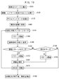
- FIG. 10 shows a flowchart of the line width measuring method of the present embodiment.
- the substrate 10 is loaded onto the stage 20 and installed (step S110).
- This substrate 10 carry-in process can be executed using the control device 40 in a configuration in which the control device 40 of the line width measuring device 100 is connected to a transport device (not shown) for transporting the substrate 10.
- a substrate transfer program for controlling the transfer of the substrate 10 is stored in the storage device 50 of the line width measuring apparatus 100.
- substrate conveyance program is operated, the stage 20 and a board
- the start of loading of the substrate 10 may be performed by an operator using the input device 62, or automatically in accordance with the completion of the operation of the previous substrate 10, for example, in accordance with the step of the line width measuring method of the substrate 10. May be executed automatically.
- a recipe corresponding to the type of substrate 10 carried in (that is, the type of the liquid crystal panel) and / or the layer of the substrate 10 (information on a predetermined layer in the laminated structure) is opened (step S120).
- the information recipe of the substrate 10 is stored in the storage device 50.
- the step of opening the recipe may be executed in synchronization with the step of carrying in the substrate 10.
- the operator designates the type of the board 10 using the input device 62 (for example, a mouse), and at the same time, while loading the board 10,
- the recipe for the substrate 10 may be opened.
- the operator does not specify the substrate 10 with the input device 62, but reads the type of the substrate 10 with a sensor or the like, and automatically loads the substrate 10 and / or opens the recipe for the substrate 10. It doesn't matter.
- the recipe for the substrate 10 includes the type of the substrate 10 (model of the liquid crystal panel), the layer information of the substrate 10, and the information on the pattern to be measured (pattern 45 in FIG. 7B) (all registered coordinates, all And the movement pattern of the camera 30 are also included.
- the recipe (recipe data) of the substrate 10 may be stored in the camera magnification switching device 55 in addition to being stored in the storage device 50.
- step S130 the camera 30 is moved by the camera moving device 32, and an alignment mark serving as a coordinate reference is read (step S130). Specifically, step S130 of moving the camera moving device 32 so that the camera 30 captures the alignment mark is executed.
- the alignment mark is often provided in a non-display area of the substrate 10. In the example shown in FIG. 2, alignment marks (for example, a cross mark extending in the XY direction) can be provided in an area of the mother glass 110 excluding the panel area 115.
- step S130 when the camera 30 reads the alignment mark, the positional deviation at the time of loading the substrate 10 can be canceled.
- the error can be suppressed to be smaller when the alignment mark formed on the substrate 10 is set as the reference point than when the predetermined position of the stage 20 of the line width measuring apparatus 100 is set as the reference point.
- the camera 30 is moved to the specified coordinates (step S140). Specifically, the camera 30 is moved to the first specified coordinates (first specified coordinates) with reference to the alignment mark. Therefore, the camera magnification switching device 55 sets the camera magnification (second camera magnification) to a low magnification (for example, 20 times) and executes a pattern search (step S142).
- the pattern search in step S142 is not a search for measuring the line width of the pattern to be measured, but a search for recognizing the pixel region. Specifically, as shown in FIG. 8, by searching the color identification mark 47 in the field area 82 of the second camera magnification (for example, low magnification such as 20 times), the pixel area (for example, A green (G) pixel region) is recognized. It is also possible to change to the second camera magnification before moving in step S140.
- the first camera magnification for example, a normal magnification such as 50 times
- a predetermined picture element area for example, a green (G) picture element area
- a field area 82 having a second camera magnification (20 times) is represented by a first camera magnification ( 50) to the visual field area 84.
- step S150 a step of searching for a registered pattern from the image data of the visual field region 84, that is, a pattern recognition step is executed (step S150). Specifically, as shown in FIG. 7, the same pattern as the measurement target pattern (registered recognition pattern) 45 stored in the storage device 50 of the present embodiment is recognized from the image data of the visual field region 80.
- the line width is measured from the image data captured in the visual field region 80 including the pattern 45 (step S160).
- the line width of the gate wiring 41, the line width of the source wiring 42, the line width of the drain wiring 43, the dimensions of the semiconductor layer 44, the source electrode 46s, and the drain electrode 46d is measured.
- the line width measurement in step S160 is executed by storing the image data captured by the camera 30 in the storage device 50 and analyzing the image data by the image analysis program 52.
- various line widths for example, the line width of the gate wiring 41
- various line widths are calculated from the image data of the visual field region 80 by the functions of the storage device 50 and the control device 40. be able to.
- edge processing of the image data captured by the camera 30 is necessary, the edge processing of the wiring image data included in the image data is performed by a typical edge processing program, and based on the data after the edge processing. Calculate the line width.
- the line width measurement can be performed by specifying edges (lines at both ends) extending in the extending direction from the image data pattern (for example, the pattern of the gate wiring 41) and calculating the distance between the edges.
- step S170 when the line width measurement in step S160 is completed, the process moves to the next measurement point (step S170). Specifically, based on the recipe information read out in step S120, the camera 30 is moved to specified coordinates (that is, second specified coordinates).
- specified coordinates that is, second specified coordinates.
- step S150 When searching for a registered pattern at the next measurement point (step S150), the above-described steps S142, S144, and S146 are executed, and the registration recognition pattern 45 is recognized there (step S152). Subsequently, the line width is measured from the image data captured in the visual field region 80 including the pattern 45 as in the previous case (step S160).
- Step S170 move from the second specified coordinates to the next specified coordinates (third specified coordinates). To do.
- the same steps (S142 to S160) are executed for the third specified coordinates, and then the third specified coordinates are moved to the next specified coordinates (fourth specified coordinates) (step S170).
- the step is executed for all measurement points (specified coordinates). That is, the above-described steps are executed for all the specified coordinates.
- a step of unloading the substrate 10 is executed (S180).
- the movement control of the camera 30 by the control device 40 is strictly performed.
- an error tolerance
- the error also has a peculiarity. Specifically, due to the influence of the motor that moves the camera 30 (the drive unit of the camera moving device 32) and the weight of the camera 30, the movement of the camera 30 moves (moves with a certain probability). Position misalignment) may occur.
- step S154 the periphery of the visual field region 80 is searched. More specifically, if the search in step S150 is executed and the registration recognition pattern 45 cannot be recognized, the vicinity of the visual field region 80 is searched (step S154). If pattern recognition can be executed in the peripheral search in step S154 (step S156), line width measurement is executed (step S160).
- the step (S142) of searching for a pattern with the second camera magnification (low magnification) is executed, so the number of times that steps S154 and S156 are executed is reduced or almost all. Does not occur. This is because even if the camera 30 is displaced, it is possible to absorb the displacement of the registered coordinates due to the displacement in step S142.
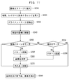
- FIG. 11 is a flowchart for explaining a line width measuring method according to a comparative example.
- the substrate 10 is carried onto the stage 20 (step S210).
- the recipe corresponding to the type of substrate 10 and / or the layer of substrate 10 is opened (step S220).
- the camera 30 is moved by the camera moving device 32, and an alignment mark serving as a reference for coordinates is read (step S230).
- the camera 30 is moved to the specified coordinates (step S240). Specifically, the camera 30 is moved to the first specified coordinates (first specified coordinates) with reference to the alignment mark. In this step S240, since the data of movement shift (registered coordinate correction value) is not added to the first specified coordinates, the camera 30 uses the first specified coordinates (first registered coordinates) as per the recipe. Move to.
- the same pattern as the measurement target pattern (registered recognition pattern) 45 is searched from the image data of the visual field area 80 at the first specified coordinates (first specified coordinates) (step S250).
- the registration recognition pattern 45 may not be included in the visual field region 80 at the first specified coordinates. That is, in this comparative example, the step (S142) of searching for a pattern with the second camera magnification (low magnification) in the present embodiment is not executed, so the registration recognition pattern 45 is included in the visual field region 80 at the first specified coordinates. The probability that failure will occur is relatively high.
- step S250 When the search in step S250 is executed and the step of recognizing the registration recognition pattern 45 (S252) can be executed, the line width is measured from the image data captured in the visual field region 80 including the registration recognition pattern 45 (step S252). S260).
- step S250 when the search in step S250 is executed and the registration recognition pattern 45 cannot be recognized, the periphery of the visual field region 80 is searched (step S254).
- This peripheral search is executed on the assumption that the registration recognition pattern 45 exists around the visual field region 80.
- the viewing area 80 exists in the adjacent picture element area due to the displacement of the camera 30, for example, the registration recognition pattern 45 as a target is immediately found by this peripheral search (step S254). Is difficult. Therefore, it may take a considerable time for the peripheral search in step S254.
- the line width is measured from the image data captured by the camera 30 (step S260).
- step S260 After completion of the line width measurement step (S260) at the first specified coordinates, the process moves to the next measurement point (step S270). And step S250, step S252, step S260 or step S254, step S256 is executed also in the second specified coordinates.
- step S254 if the peripheral search (step S254) is executed even with the second specified coordinates, it takes a long processing time here. These processes are performed for all the specified coordinates, but a long processing time is required every time the peripheral search (step S254) is executed.
- the substrate 10 is unloaded (step S280).
- the pattern to be measured can be imaged by the camera 30 having a first camera magnification (for example, 50 times) that measures the line width of the pattern to be measured (Steps S146, S150, S152, and S160). ). Accordingly, it is possible to suppress erroneous measurement such as measuring the pixel area of the adjacent color due to the movement shift of the camera 30.
- the processing time for line width measurement can be reduced by reducing the number of times of the peripheral search (step S154 and step S254) or making the peripheral search execution substantially zero.
- the first camera magnification is set to 50 times and the second camera magnification (low magnification) is set to 20 times.
- the camera magnification is suitably suitable according to the substrate 10 to be measured. Can be used.
- the first camera magnification (normal magnification) may be 30 to 100 times
- the second camera magnification (low magnification) may be 10 to 25 times.
- the measurement of the line width in the array substrate for displaying four primary colors of red (R), green (G), blue (B), and yellow (Y) has been described. If it is a substrate (for example, an array substrate displaying four primary colors of red (R), green (G), blue (B), white (W), or an array substrate displaying five primary colors or six primary colors), this embodiment This technique can be applied to other substrates.
Landscapes
- Physics & Mathematics (AREA)
- General Physics & Mathematics (AREA)
- Length Measuring Devices By Optical Means (AREA)
Abstract
被測定対象を正確に且つ効率的に測定することが可能な線幅測定装置を提供する。測定対象のパターンの線幅を測定する線幅測定装置100であり、測定対象のパターンを撮像するカメラ30と、カメラ移動装置32と、カメラ移動装置32の移動を制御する制御装置40とを備える。測定対象のパターンは、少なくとも4原色の表示による液晶パネル用の基板10に形成されており、制御装置40は、カメラ30が撮像したパターンを画像解析する画像解析プログラム52が格納された記憶装置50に接続されている。そして、制御装置40は、測定対象のパターンの線幅を測定する第1カメラ倍率(通常倍率:例えば50倍)と、基板10に含まれる絵素領域を認識する第2カメラ倍率(低倍率:例えば20倍)とを切り替えるカメラ倍率切替装置55に接続されている。制御装置40は、第2カメラ倍率を有するカメラ30にて絵素領域を認識した後、第1カメラ倍率を有するカメラ30にて測定対象のパターンを撮像するようにカメラ30を制御する。
Description
本発明は、線幅測定装置に関する。特に、大型ガラス基板上に形成されたパターン線幅または間隔を測定する線幅測定装置に関する。
なお、本出願は2011年2月17日に出願された日本国特許出願2011-31563号に基づく優先権を主張しており、その出願の全内容は本明細書中に参照として組み入れられている。
なお、本出願は2011年2月17日に出願された日本国特許出願2011-31563号に基づく優先権を主張しており、その出願の全内容は本明細書中に参照として組み入れられている。
線幅測定装置または寸法測定装置は、液晶パネル用の基板(例えば、TFT基板)のパターン線幅または間隔、あるいは、半導体装置を製造するためのマスクのパターン線幅または間隔を測定する装置である(例えば、特許文献1)。線幅測定装置(または寸法測定装置)は、例えば、透明ガラス基板の上に形成された膜パターンに照明を照射して得られるパターン像を顕微鏡で拡大した後、その画像をイメージセンサ(例えばCCDカメラ)で撮像して得られるパターン像を画像処理することによって、寸法または形状を測定する。ここでは、線幅測定装置、寸法測定装置、線幅検査装置または寸法検査装置を「線幅測定装置」と称する。
液晶表示装置(LCD)の構成部品である液晶パネルは、一対のガラス基板を所定のギャップを確保した状態で対向させた構造を有している。液晶パネルの大型化・量産化に伴って、液晶パネル用のガラス基板(マザーガラス)は年々大型化している。マザーガラスは、例えば、1辺が1mを越えるようになっている(例えば、1100mm×1300mm(第5世代基板)から、2880mm×3130mm(第10世代基板))。そして、その大型化したマザーガラスから、1枚の液晶パネルに相当する部位が多数個取り出される。したがって、被測定対象物のマザーガラスには、同じ形状の検査すべき膜パターンが複数個存在する。
被測定対象物がマザーガラスのような基板の場合、それに伴って、被測定対象物上に形成される膜パターンの露光誤差(位置ズレ)は一般的に増加する傾向にある。ここで、被測定対象物上に形成される膜パターンの位置ズレが大きくなる結果、線幅測定装置では、所定の測定位置を撮像するためにXYステージを移動しても、被対象物上でのパターン位置がずれているために、撮像した映像内に必要な被測定箇所の一部がはみ出すことがある(例えば、特許文献2)。
上述の露光誤差(位置ズレ)の増大を小さくするために、あるいは、所定の測定位置を撮像するためにXまたはY方向に試料台を移動した場合に、撮像した映像内に画像処理に必要な被測定箇所の一部がはみ出す状況をできるだけ少なくすることが必要である。このために、従来は、被測定対象物を試料台上に搬送ロボット等によって搬入し、試料台の上に、X及びY方向にそれぞれ固定ピン等の位置決め用ストッパを設けていた。そして、一度試料台上に載置してから、ストッパに対してX及びY方向に被測定対象物を押し付けて位置決め精度を向上させていた。しかる後、例えば、吸着機構によって吸着し、被測定対象物を試料台に固定していた。
また更に、拡大画像による微細な寸法を測定しようとする線幅測定装置において、複数の撮像ヘッド部を設けたマルチ撮像ヘッドによる測定を行う場合にも、上記と同様に、被測定対象物の位置ズレを小さくするための位置決め機構を設けている。そして、その位置決め機構により、測定の精度、シーケンスを損なわないように被測定対象物の位置決めを、搬送ロボット等による搬入時に行っていた。さらには、被測定対象物の大型化に伴って、その質量、静電気などの影響によって被測定対象物を動かすこと自体が困難になり、強制的な位置決めが難しくなり、位置決め動作不良が多く発生するようにもなってきた。そのため、搬入時の位置決め動作ではなく、撮像ヘッド部の方の位置を移動させて、アライメント補正処理を行うことも提案されている(例えば、特許文献1)。
図1は、特許文献1に開示された線幅測定装置500の概略構成を示すブロック図である。図1に示した線幅測定装置500は、測定部501を備えている。測定部501は、撮像ヘッド部508、試料台509、位置補正部510、エアー除振台512、照明用電源513、ステージ制御部520、透過照明用電源521、透過照明ヘッド部522から構成されている。撮像ヘッド部508は、観察用カラーカメラユニット、測定カメラユニット、電動レボルバユニット、レーザーオートフォーカスユニットなどから構成されている。また、線幅測定装置501には、カラーモニタ514、測定用モニタ515、測定結果表示用モニタ516が設けられている。さらに、線幅測定装置501には、ビデオプリンタ517、画像処理PC(Personal Computer)518、制御PC519が設けられている。
線幅測定装置500では、撮像ヘッド部508の観察用カラーカメラで撮られた画像はカラーモニタ514に表示され、測定カメラで撮られた画像は測定用モニタ515に表示される。線幅測定装置500は、外部ホスト(HOST)または制御PC519の指令によって測定を開始する。当該測定は、予め設定されたレシピに基づいて、自動またはマニュアル動作で開始され、その測定結果は、測定結果表示用モニタ516に表示される。そして、測定結果は、例えば制御PC519内のHD(Hard Disk)等の記憶装置の所定エリアに書き込まれる。また、それらの測定結果データは、外部ホストの要求によって、外部ホストに配信される。なお、エアー除振台512によって、外部の振動が試料台509に伝わらないようにしている。
画像処理PC518は、撮像ヘッド部508から入力された画像を解析して、被測定対象物中に予め設定された所定のパターンを認識する。そして、その位置座標を取得して、補正量を求める。求めた補正量の情報は、制御PC519に出力され、制御PC519は、ステージ制御部520に、補正量の情報に基づいて制御指示信号を出力する。ステージ制御部520は、入力された制御指示信号に対応する制御信号を位置補正部510に与えることによって、位置補正を行う。このように、図1に示した線幅測定装置500では、位置補正部510による補正によって、機械的に被測定対象物の搭載位置を強制的に動かすことができない場合であっても位置ズレ補正を行うことができる。
特許文献1に開示された線幅測定装置500では、位置補正部510による補正によって位置ズレの補正を行うことができる。しかしながら、本願発明者の検討によると、そのような搬入時における位置ズレ補正を行っても、線幅測定装置のカメラを一度移動させるだけでは、そのカメラ内に被測定部位がおさまらないケースが生じることがわかった。以下、さらに説明する。
図2は、所定寸法の液晶パネル部分(115)が多面取りされるマザーガラス110の上面を模式的に示している。図2に示したマザーガラス110は、第10世代のマザーガラスであり、例えば、2880mm×3130mmの寸法を有している。ここで、マザーガラス110内の各パネル領域115は、40インチの液晶パネルに相当するものである。各パネル領域115の一部を拡大すると、そのパネル領域115がアレイ基板(TFT基板)の一部であるときは、例えば、図3に示すようなパターンを含んでいる。
具体的には、アレイ基板112の上面(アレイ基板112の液晶層の側の面、すなわち、カラーフィルタ基板に対向する面)には、スイッチング素子(例えば、TFT)144および画素電極146が設けられている。スイッチング素子144および画素電極146の周りには、格子状をなすように、ソース配線141およびゲート配線142が取り囲むようにして設けられている。ソース配線141およびゲート配線142がそれぞれ、スイッチング素子144のソース電極およびゲート電極に接続されている。画素電極146は、例えば、ITO(インジウム・スズ・オキサイド)から構成されている。画素電極146は、例えば、矩形状に形成され、図3に示した例では、ソース配線141が延びる方向に沿って細長い長方形の形状に形成されている。
線幅測定装置は、図3に示したパターンの一部(例えば、ソース配線141の幅など)を測定し、その良否を判定していく。図3に示したようなパターンの一部(例えば、ソース配線141の幅など)は、図2に示したパネル領域115の中に膨大にあり、さらに、そのパネル領域115は、マザーガラス110に複数個配置されている。したがって、線幅測定装置が測定すべきポイントは、非常に多数存在し(例えば、約350点またはそれ以上)、そのポイントを如何に正確に且つ効率的に測定していくかが大きなテーマとなる。
図4に示したマザーガラス110は、図3に示したようなパターンが形成されたアレイ基板112である。線幅測定装置の一台のカメラは、マザーガラス110の上半分領域111aを撮像し、一方、線幅測定装置のもう一台のカメラは、マザーガラス110の下半分領域111bを撮像する。ここで、本願発明者の検討によれば、上半分領域111aのカメラ検査では、ほぼ一度の移動で正常に撮像できたが、下半分領域111bのカメラ検査では、一度の移動では、ほぼ全ての測定ポイントにおいて正常に撮像できなかったケースが観測された。
簡単に述べると、上半分領域111aでは、カメラを移動させると、そのカメラ位置に測定対象のパターンが含まれるが、下半分領域111bで、カメラを移動させても、そのカメラ位置に測定対象のパターンが含まれない。したがって、下半分領域111bでは、一度カメラを移動させた後、周囲に測定対象のパターンがないかどうかカメラを移動させ、測定対象のパターンを見つけてから、当該測定対象のパターンを測定する処理が必要である。それゆえに、上半分領域111aと比較して、下半分領域111bの測定時間は、非常に多くかかり、それは当然スループットの低下につながる。
ここで、二台のカメラとも、搬入時における搭載位置の位置ズレに対する補正を実行しているので、両カメラの位置ズレの問題は本来は無いはずである。しかしながら、実際には、一方のカメラでは、一度の移動で撮像および測定ができ、他方のカメラでは、一度の移動では撮像ができず周囲をサーチしてからでないと、撮像および測定ができない事象が存在する。このような状態で測定を行う線幅測定装置をそのままにしておけば、測定の作業効率が悪いだけでなく、線幅測定の誤作動を見逃してしまう可能性すらある。
ところで、赤(R)、緑(G)、青(B)の3原色からなるカラーフィルタを用いた液晶パネルの他に、近年、より広い色再現範囲を表示可能にするために、赤(R)、緑(G)、青(B)、黄(Y)の4原色からなるカラーフィルタを用いた液晶パネルが提案されている(例えば、特許文献3)。3原色の液晶パネルの場合には、各色の画素領域の大きさは同じであるが、4原色の液晶パネルの場合、各色の画素領域の大きさは同じでない。すなわち、各色の画素領域におけるTFT基板の形状はそれぞれ異なるので、カメラの移動ズレによって、隣の色の画素領域を測定してしまうと、誤った測定結果を算出してしまうことになり問題である。
本発明はかかる点に鑑みてなされたものであり、その主な目的は、被測定対象を正確に且つ効率的に測定することが可能な線幅測定装置を提供することにある。
本発明に係る線幅測定装置は、測定対象のパターンの線幅を測定する線幅測定装置であり、測定対象のパターンを撮像するカメラと、前記カメラを移動させるカメラ移動装置と、前記カメラ移動装置の移動を制御する制御装置とを備え、前記測定対象のパターンは、少なくとも4原色の表示による液晶パネル用の基板に形成されており、前記制御装置は、前記カメラが撮像した前記パターンを画像解析する画像解析プログラムが格納された記憶装置に接続されており、そして、前記制御装置は、前記測定対象のパターンの線幅を測定する第1カメラ倍率と、前記第1カメラ倍率よりも低い倍率で、前記基板に含まれる絵素領域を認識する第2カメラ倍率とを切り替えるカメラ倍率切替装置に接続されており、前記制御装置は、前記第2カメラ倍率を有する前記カメラにて前記絵素領域を認識した後、前記第1カメラ倍率を有する前記カメラにて前記測定対象のパターンを撮像するように前記カメラを制御する。
ある好適な実施形態では、さらに、前記基板が載置されるステージを備えており、前記基板は、4原色表示の液晶パネル用のマザーガラスであり、前記測定対象のパターンの画像データは、前記記憶装置に登録されており、前記制御装置は、前記カメラに撮像された前記測定対象のパターンと、前記記憶装置に登録された前記測定対象のパターンの前記画像データとを照合する機能を有している。
ある好適な実施形態において、前記測定対象のパターンが形成された基板には、基準位置を示すアライメントマークが設けられており、前記画像解析プログラムは、前記カメラが前記アライメントマークを撮像するように前記カメラ移動装置を移動させるステップと、前記アライメントマークを基準にして、第1の規定座標に前記カメラを移動させるステップと、前記第1の規定座標において、前記第2カメラ倍率で前記絵素領域を認識するステップと、前記第2カメラ倍率から前記第1カメラ倍率に切り替えるステップと、前記第1カメラ倍率にて、前記記憶装置に登録された登録パターンと同一パターンをサーチするステップと、前記サーチによって、前記第1の規定座標における前記測定対象のパターンを認識するステップと、前記認識された前記測定対象のパターンの線幅を測定するステップと、前記第1の規定座標から、前記第2の規定座標に前記カメラを移動させるステップとを含む。
ある好適な実施形態において、前記基板には、前記4原色表示における色を示す色識別マークが形成されており、前記絵素領域を認識するステップでは、前記カメラが前記色識別マークを撮像することによって実行される。
ある好適な実施形態において、前記画像解析プログラムは、前記第2の規定座標に前記カメラを移動させた後、前記第2の規定座標において、前記第2カメラ倍率で前記絵素領域を認識するステップと、前記第2カメラ倍率から前記第1カメラ倍率に切り替えるステップと、前記第1カメラ倍率にて、前記記憶装置に登録された登録パターンと同一パターンをサーチするステップと、前記サーチによって、前記第2の規定座標における前記測定対象のパターンを認識するステップと、前記認識された前記測定対象のパターンの線幅を測定するステップと、前記第2の規定座標から、前記第3の規定座標に前記カメラを移動させるステップとを含む。
ある好適な実施形態において、前記画像解析プログラムは、前記全ての規定座標における前記測定対象のパターンの線幅を測定するステップが実行された後、前記基板を搬出するステップを実行する。
ある好適な実施形態において、前記カメラは、少なくとも第1撮像部と第2撮像部とを含んでいる。
本発明に係る線幅測定方法は、測定対象のパターンの線幅を測定する線幅測定方法であり、少なくとも4原色の表示による液晶パネル用の基板をステージの上に搬入する工程と、前記基板の種類およびレイヤの情報を取得する工程と、前記基板に形成されたアライメントマークを、カメラで撮像する工程と、前記アライメントマークを基準にして、第1の規定座標に前記カメラを移動させる工程と、前記第1の規定座標において、前記第2カメラ倍率で前記絵素領域を認識する工程と、前記第2カメラ倍率から、前記第2カメラ倍率よりも高い倍率を有する第1カメラ倍率に切り替える工程と、前記第1カメラ倍率にて、前記記憶装置に登録された登録パターンと同一パターンをサーチする工程と、前記サーチによって、前記第1の規定座標における前記測定対象のパターンを認識するステップと、前記認識された前記測定対象のパターンの線幅を測定する工程と、前記第1の規定座標から、前記第2の規定座標に前記カメラを移動させる工程とを含む。
本発明の線幅測定装置によれば、絵素領域を認識する第2カメラ倍率を有するカメラにて絵素領域を認識した後、測定対象のパターンの線幅を測定する第1カメラ倍率を有するカメラにて測定対象のパターンを撮像する。したがって、カメラの移動ズレが生じることによって隣の色の画素領域を測定することを抑制することができる。その結果、少なくとも4原色の表示による液晶パネル用の基板に形成された測定対象のパターンの線幅を測定する線幅測定装置を実現することができる。
以下、図面を参照しながら、本発明の実施形態を説明する。以下の図面においては、説明の簡潔化のために、実質的に同一の機能を有する構成要素を同一の参照符号で示す。なお、本発明は以下の実施形態に限定されない。
図5は、本発明に係る実施形態の線幅測定装置100の構成を模式的に示すブロック図である。本実施形態の線幅測定装置100は、測定対象のパターンの線幅を測定する線幅測定装置であり、線幅測定装置の他、寸法測定装置、線幅検査装置または寸法検査装置と称してもよいが、本実施形態では、「線幅測定装置」と称する。
本実施形態の線幅測定装置100は、測定対象のパターンを撮像するカメラ30と、カメラ30を移動させるカメラ移動装置32と、カメラ移動装置32の移動を制御する制御装置40とから構成されている。本実施形態の測定対象のパターンは、少なくとも4原色の表示による液晶パネル用の基板に形成されている。
また、本実施形態の制御装置40は、カメラ30が撮像したパターンを画像解析する画像解析プログラム52が格納された記憶装置50に接続されている。画像解析プログラム52は、カメラ30が撮像したパターンを含む画像データから、当該パターンの線幅(または間隔)を測定することができるプログラムである。
本実施形態のカメラ30は、例えば、CCDイメージセンサ、または、CMOSイメージセンサなどである。本実施形態のカメラ移動装置32は、カメラ30をX-Y方向に移動可能な機械式装置である。また、本実施形態の制御装置40は、半導体集積回路からなり、例えばMPU(マイクロ・プロセッシング・ユニット)またはCPU(セントラル・プロセッシング・ユニット)である。
本実施形態の記憶装置50は、例えば、ハードディスク(HDD)、半導体メモリ、光ディスク、光磁気ディスクなどである。また、制御装置40には、入力装置62(キーボード、マウス、タッチパネルなど)および出力装置64(ディスプレイなど)が接続されている。本実施形態の制御装置40、記憶装置50、入力装置62、出力装置64は、汎用のPC(パーソナル・コンピュータ)のものを適用することができる。
また、本実施形態の制御装置40は、第1カメラ倍率(例えば、50倍)と、第2カメラ倍率(例えば、20倍)とを切り替えるカメラ倍率切替装置55に接続されている。第1カメラ倍率(例えば、50倍)は、測定対象のパターンの線幅を測定する倍率である。一方、第2カメラ倍率(例えば、20倍)は、第1カメラ倍率(例えば、50倍)よりも低い倍率で、基板に含まれる絵素領域を認識する倍率である。
なお、本実施形態のカメラ倍率切替装置55は、カメラ30が撮像した画像データをソフトウエア的に拡大・縮小する装置であり、言い換えると、カメラ30が撮像した画像データの倍率を変更するプログラムを備えた装置である。本実施形態のカメラ倍率切替装置55を構築するプログラムは、記憶装置50と同じ部材の中に格納されており、例えば、ハードディスク(HDD)、半導体メモリなどの中に格納されている。カメラ倍率切替装置55を構築するプログラムは、記憶装置50の一部に格納してもよいし、記憶装置50とは別の装置内に格納してもよい。記憶装置50がハードディスクの場合、そのハードディスクの一部に、カメラ倍率切替装置55を構築するプログラムを格納することができる。なお、カメラ倍率切替装置55は、ソフトウエア的な装置に限らず、カメラ30の倍率を光学的に変更する装置であっても構わない。
本実施形態では、制御装置40は、第2カメラ倍率(例えば、20倍)を有するカメラ30にて絵素領域を認識した後、第1カメラ倍率(例えば、50倍)を有するカメラ30にて測定対象のパターンを撮像するようにカメラ30を制御する。すなわち、カメラ30は、一度、広範囲を撮像してターゲットとなる絵素領域(例えば、緑(G)絵素領域)を特定した後、ターゲットとなる絵素領域(例えば、緑(G)絵素領域)に含まれる測定対象のパターンを撮像する。これにより、カメラ移動装置32によるカメラ30の移動に移動ズレが生じたとしても、最初に、ターゲットとなる絵素領域を認識し、次いで、その絵素領域内の測定対象のパターンの線幅を測定することができる。したがって、赤(R)、緑(G)、青(B)、黄(Y)の4原色からなるカラーフィルタを用いた液晶パネルの線幅測定において、カメラの移動ズレが生じても、隣の色の絵素領域を測定してしまうという誤った測定を回避することができる。
なお、カメラ30の移動ズレは、基板をステージ20上に搬入する際に生じる位置決めのズレではなく、カメラ30の移動に伴う座標ズレのデータである。カメラ30の移動に伴う座標ズレの発生の原因は、かなり詳細に特定しても掴みきれないことが多い。したがって、その座標ズレが生じた時においては、カメラ移動装置32の移動は所定座標にカメラ30を移動させたことになっているので、カメラ30がターゲットの絵素領域の測定対象のパターンを撮像しているのか、ターゲットとは別の絵素領域(例えば、隣の絵素領域)の測定対象のパターンを撮像しているのかは特定できない場合が多い。
特に、赤(R)、緑(G)、青(B)、黄(Y)の4原色からなるカラーフィルタを用いた液晶パネルの場合には、それぞれの絵素領域の寸法(面積)が異なる。それゆえに、狭い絵素領域(例えば、緑(G)領域)内の測定対象のパターンを撮像しようとして、移動ズレにより、隣の絵素領域(例えば、青(B)領域)内の同種の測定対象パターンを撮像してしまう可能性があるとともに、そのエラーに気がつきにくい。なお、赤(R)、緑(G)、青(B)の3原色からなるカラーフィルタを用いた液晶パネルの場合、各絵素領域の寸法(面積)は同じである(または実質的に同じである)ので、移動ズレにより、隣の絵素領域(例えば、青(B)領域)内の同種の測定対象パターンを撮像してしまう可能性は少ない。したがって、本実施形態の線幅測定装置100は、赤(R)、緑(G)、青(B)、黄(Y)の4原色からなるカラーフィルタを用いた液晶パネルにおける線幅測定する際に特に効果を奏する。
本実施形態では、各色を表示する最小単位を「絵素」又は「絵素領域」と称する。一方で、カラー表示を行うための最小単位を「画素」または「画素領域」と称する。赤(R)、緑(G)、青(B)、黄(Y)の4原色表示の液晶パネルの場合、赤(R)、緑(G)、青(B)、黄(Y)の「絵素領域」を1つのまとまりの単位として「画素領域」と称する。ここで、「画素領域」をピクセルと称するならば、「絵素領域」をサブピクセルと称しても構わない。この関係は、3原色表示の液晶パネルでも、4原色を越える表示(5原色以上)の液晶パネルでも同様である。
図6(a)及び(b)は、本実施形態の線幅測定装置100においてカメラ30を移動させる様子を示す工程図である。
まず、図6(a)に示すように、ステージ20の上に基板10を搬入する。基板10は、例えば、ガラス基板であり、本実施形態における基板10は、液晶パネル用のガラス基板である。上述したように、本実施形態の基板10は、少なくとも4原色の表示による液晶パネル用の基板(アレイ基板)であり、この例では、赤(R)、緑(G)、青(B)、黄(Y)の4原色の表示を行う基板(アレイ基板)である。
図示した例の基板10は、液晶パネルの寸法に切り出す前のマザーガラスである。基板10としてのマザーガラスの寸法は1辺が1メートル以上あり、具体的には、基板10が第10世代のマザーガラスの場合、その寸法は2880mm(W)×3130mm(L)である。図示した基板10は、TFT(薄膜トランジスタ)および/または配線が形成されたアレイ基板である。基板10がマザーガラスである場合の一例は、図2に示す通りであり、基板10がアレイ基板である場合のパターンの一例は、図3に示す通りである。
ステージ20上に基板10が搬入されるタイミング(矢印70参照)で、基板10の内部からピン22が浮上して、ピン22の先端で基板10を支持する。ステージ20の上方には、カメラ30が配置されており、このカメラ30は、カメラ移動装置32によってステージ20の範囲(所定のX-Y座標)を移動することができる。カメラ移動装置32は、カメラ30を例えば50μm~80μmの精度で(典型的には、精度60μmで)移動させることができる。
次に、図6(b)に示すように、ステージ20の内部にピン22を収納し、ステージ20の表面に基板10を配置する。ステージ20の表面に配置された基板10は、カメラ30によって撮像されて、そのカメラ30の画像を解析することによって、基板10におけるパターンの線幅が測定される。本実施形態では、カメラ30は、基板10において登録されている座標ポイント(例えば、約350点またはそれ以上)に移動し(矢印72参照)、そのポイントで撮像を行う。カメラ30の移動は、上述したように、制御装置40によって制御されるカメラ移動装置32によって行われる。また、基板(マザーガラス)10には、基準位置を表すアライメントマークが形成されており、そのアライメントマーク(例えば、+字マーク)を基準にしてカメラ30を移動させることもできる。
本実施形態の線幅測定装置100におけるカメラ30は、1枚の基板10に対して1つであっても構わないが、2つにすることもできる。例えば、図4に示したように、2つのうちの1つのカメラ30を基板の上半分111aの撮像用にし、もう1つのカメラ30を下半分111bの撮像用にすることができる。基板10が1メートルを超えるマザーガラスの場合、カメラ30の移動距離は非常に長くなるので、複数のカメラ30を用いる技術的なメリットは大きい。なお、カメラ30は、2つに限らず、それ以上(例えば、4つ)使用することもできる。
次に、図7を参照しながら、線幅測定装置100によって線幅を測定する方法について説明する。
図7(a)は、基板10(アレイ基板)における所定の絵素領域のパターンを示している。図示した例では、行方向(横方向)にゲート配線41が延び、列方向(縦方向)にソース配線42が延びている。ゲート配線41とソース配線42との交点には、半導体層(例えば、シリコン層)44が形成されている。半導体層44の表面には、ソース配線42から延びたソース電極46sと、ドレイン配線43から延びたドレイン電極46dとが形成されている。図7(a)に示した領域80は、カメラ30の視野領域である。
図7(b)は、本実施形態の記憶装置50に格納されている測定対象のパターン(登録認識パターン)45である。この例では、線幅測定を行うための登録認識パターン45は、ゲート配線41の一部41aと、ドレイン配線43の一部43aが登録されている。この登録認識パターン45は、図7(a)における領域80内に位置するものである。そして、線幅測定装置100は、登録認識パターン45を認識してから、所定パターンの線幅(例えば、ゲート配線41の線幅、ソース配線42の線幅など)を測定する。具体的には、線幅測定装置100は、基板10において登録されている座標ポイント(例えば、約350点またはそれ以上)に移動した後、そこで、登録認識パターン45を認識し、次いで、所定パターンの線幅の測定を実行する。
図8は、赤(R)、緑(G)、青(B)、黄(Y)の4原色表示のアレイ基板における画素領域を示している。ここでは、緑(G)の絵素領域に、色識別マーク47が設けられている。なお、図示した例では、赤(R)及び青(B)の絵素領域の面積と比較して、緑(G)および黄(Y)の絵素領域の面積が小さい構造となっている。また、図9は、緑(G)の絵素領域を拡大して示した図である。図8および図9においては、便宜上、ゲート配線41およびソース配線42のパターンを示している。
まず、図8に示すように、カメラ30は、第2カメラ倍率(例えば、20倍)の視野領域82にて、基板10に含まれる絵素領域(R・G・B・Y)を認識する。ここでは、緑(G)の絵素領域に設けられた色識別マーク47を撮像することによって、緑(G)の絵素領域を認識する。
次に、図9に示すように、カメラ30は、カメラ倍率切替装置55によって第2カメラ倍率(例えば、20倍)から第1カメラ倍率(例えば、50倍)に変更し、そして、第1カメラ倍率(例えば、50倍)の視野領域84にて、所定の絵素領域(ここでは、緑(G)の絵素領域)の測定対象パターンを撮像する。図9に示した状態においては、線幅測定装置100は、図7に示したように、まず、登録認識パターン45を認識してから、所定パターンの線幅(例えば、ゲート配線41の線幅、ソース配線42の線幅など)を測定する。その後は、次の座標ポイントに移動して、同様の工程を繰り返し実行する。
このように、本実施形態の線幅測定装置100を用いた線幅測定によれば、絵素領域(R・G・B・Y)を認識する倍率(第2カメラ倍率)を有するカメラ30(視野領域82)にて絵素領域を認識した後、測定対象のパターンの線幅を測定する倍率(第1カメラ倍率)を有するカメラ30(視野領域84)にて測定対象のパターンを撮像することができる。したがって、カメラ移動装置32によるカメラ30の移動ズレが生じたとしても、先に、ターゲットとなる絵素領域(例えば、G)を認識することができるので、別の絵素領域に含まれるパターンを測定するようなエラーを抑制することができる。
次に、図10を参照しながら、本実施形態の線幅測定装置100を用いた線幅測定方法の一例について説明する。図10は、本実施形態の線幅測定方法のフローチャートを示している。
まず、基板10をステージ20の上に搬入して設置する(ステップS110)。この基板10の搬入工程は、線幅測定装置100の制御装置40と、基板10を搬送する搬送装置(不図示)とを接続した構成で、制御装置40を用いて実行することができる。具体的には、線幅測定装置100の記憶装置50に、基板10の搬送を制御する基板搬送プログラムを格納しておく。そして、その基板搬送プログラムを動作させ、制御装置40の制御により、ステージ20および基板搬送装置(例えば、ローラーコンベア)を動かして、基板10をステージ20上に搬入する。基板10の搬入の開始は、入力装置62を用いて作業者が実行してもよし、基板10の線幅測定方法のステップにあわせて、例えば1つ前の基板10の作業完了にあわせて自動的に実行するようにしてもよい。
次に、搬入された基板10の種類(すなわち、液晶パネルの機種)、及び/又は、基板10のレイヤー(積層構造における所定の層の情報)に該当するレシピを開くようにする(ステップS120)。この基板10の情報のレシピは、記憶装置50に格納されている。レシピを開く工程は、基板10の搬入工程と同調させて実行してもよい。具体的には、基板10の搬入工程(S110)において、入力装置62(例えば、マウス)を用いて作業者が基板10の種類などを指定し、それと同時に、基板10の搬入を実行しながら、基板10のレシピを開くようにすることもできる。また、作業者が入力装置62にて基板10を指定するのではなく、センサなどによって基板10の種類を読み取って、自動的に、基板10の搬入、及び/又は、基板10のレシピを開くようにしても構わない。
この基板10のレシピには、基板10の種類(液晶パネルの機種)、基板10のレイヤ情報の他、測定対象のパターン(図7(b)のパターン45)の情報(全ての登録座標、全ての登録認識パターンなど)、カメラ30の移動パターンなども含まれている。なお、基板10のレシピ(レシピデータ)は、記憶装置50に格納する他、カメラ倍率切替装置55に格納しても構わない。
次に、カメラ30をカメラ移動装置32で移動させて、座標の基準となるアライメントマークを読みに行く(ステップS130)。具体的には、カメラ30がアライメントマークを撮像するようにカメラ移動装置32を移動させるステップS130を実行する。アライメントマークは、基板10のうちの非表示領域に設けられていることが多い。図2に示した例では、アライメントマーク(例えば、X-Y方向に延びた十字方のマーク)を、マザーガラス110のうちパネル領域115を除く領域に設けることができる。
ステップS130において、カメラ30がアライメントマークを読むことで、基板10の搬入時の位置ズレをキャンセルすることができる。加えて、線幅測定装置100のステージ20の所定位置を基準点に設定するよりも、基板10に形成されたアライメントマークを基準点にする方が誤差を小さく抑えることができる。加えて、アライメントマークが複数形成されている場合、基準となるアライメントマーク同士の間隔を測定することにより、基板10における膨張・収縮、反りまたは撓みなどの情報を収集することも可能である。
次に、ステップS120で読み出したレシピの情報に基づいて、カメラ30を規定の座標に移動させる(ステップS140)。具体的には、アライメントマークを基準にして、最初の規定座標(第1の規定座標)にカメラ30を移動させる。そこで、カメラ倍率切替装置55によって低倍(例えば、20倍)のカメラ倍率(第2カメラ倍率)にして、パターンサーチを実行する(ステップS142)。
ステップS142におけるパターンサーチは、測定対象のパターンの線幅を測定するためのサーチではなく、絵素領域を認識するためのサーチである。具体的には、図8に示すように、第2カメラ倍率(例えば、20倍のような低倍)の視野領域82にて、色識別マーク47をサーチすることによって、絵素領域(例えば、緑(G)の絵素領域)を認識する。なお、ステップS140で移動する前に、第2カメラ倍率に変更しておくことも可能である。
ステップS142におけるパターンサーチによって、パターン認識が完了したら(ステップS144)、その後、線幅を測定するための第1カメラ倍率(例えば、50倍のような通常倍率)に変更する(ステップS146)。具体的には、図9に示すように、所定の絵素領域(例えば、緑(G)の絵素領域)において、第2カメラ倍率(20倍)の視野領域82を、第1カメラ倍率(50倍)の視野領域84に変更する。
次に、視野領域84の画像データから、登録パターンをサーチするステップ、すなわち、パターン認識のステップを実行する(ステップS150)。具体的には、図7に示すように、本実施形態の記憶装置50に格納されている測定対象のパターン(登録認識パターン)45と同一のパターンを、視野領域80の画像データから認識する。
登録認識パターン45と同一パターンを認識(ステップS152)した後は、パターン45を含む視野領域80において撮像されている画像データから、線幅を測定する(ステップS160)。ここでは、例えば、視野領域80の画像データから、ゲート配線41の線幅、ソース配線42の線幅、ドレイン配線43の線幅、半導体層44、ソース電極46s、ドレイン電極46dの寸法(線幅含む)のうちの少なくとも1つが測定される。
ステップS160の線幅測定は、カメラ30で撮像された画像データを記憶装置50に格納し、当該画像データを画像解析プログラム52によって画像解析することによって実行される。画像解析プログラム52を起動させた線幅測定装置100においては、記憶装置50および制御装置40の働きによって、視野領域80の画像データから各種線幅(例えば、ゲート配線41の線幅)を算出することができる。カメラ30で撮像された画像データのエッジ処理が必要であれば、典型的なエッジ処理プログラムによって、画像データに含まれる配線の画像データのエッジ処理を施して、そのエッジ処理後のデータに基づいて線幅を算出する。線幅測定は、画像データのパターン(例えば、ゲート配線41のパターン)から延長方向に延びるエッジ(両端の線)を特定し、そのエッジ間の距離を算出することによって実行可能である。
次に、ステップS160での線幅測定が終わったら、次の測定ポイントに移動する(ステップS170)。具体的には、ステップS120で読み出したレシピの情報に基づいて、カメラ30を規定の座標(すなわち、第2の規定座標)に移動させる。そして、次の測定ポイントにおいて登録パターンをサーチする場合(ステップS150)、上述したステップS142、S144、S146を実行して、そこで、登録認識パターン45を認識する(ステップS152)。続いて、先ほどと同様に、パターン45を含む視野領域80において撮像されている画像データから、線幅を測定する(ステップS160)。
第2の規定座標において、ステップS142、S144、S146、S150、S152、S160を実行した後は、ステップS170にて、第2の規定座標から、次の規定座標(第3の規定座標)に移動する。第3の規定座標においても、同様のステップ(S142~S160)を実行し、次いで、第3の規定座標から、次の規定座標(第4の規定座標)に移動し(ステップS170)、これらのステップを全ての測定点(規定座標)について実行する。すなわち、全ての規定座標において、上述したステップを実行する。全ての規定座標における測定対象のパターンの線幅を測定した後は、基板10を搬出するステップを実行する(S180)。
なお、本実施形態において、制御装置40によるカメラ30の移動制御は厳密になされている。しかし、実際には10μm程度の誤差(公差)がある。その誤差にもクセがあり、具体的には、カメラ30を移動させるモータ(カメラ移動装置32の駆動部)およびカメラ30の重量の影響によって、カメラ30の進行方向に一定確率で移動ズレ(移動の際の位置ズレ)が起こる場合がある。逆に、カメラ30の進行方向に対してブレーキをかける際の影響によって当該進行方向とは反対の方向に移動ズレ(移動の際の位置ズレ)が起きる場合がある。
そのような移動ズレにより、ステップS150において登録パターンをサーチできない場合には、視野領域80の周辺をサーチする(ステップS154)。さらに説明すると、ステップS150におけるサーチを実行し、登録認識パターン45を認識できなかった場合、視野領域80の周辺をサーチする(ステップS154)。ステップS154の周辺サーチで、パターン認識が実行できれば(ステップS156)、線幅の測定を実行する(ステップS160)。
ただし、本実施形態の線幅測定方法では、第2カメラ倍率(低倍)でパターンをサーチするステップ(S142)を実行しているので、ステップS154及びS156を実行する回数は少なくなるか、ほとんど発生しない。これは、カメラ30の移動ズレが生じても、ステップS142にてその移動ズレによる登録座標のズレを吸収することができるからである。
なお、本実施形態のカメラ倍率切替装置55を用いずに線幅測定を行う比較例について、図11を参照しながら説明する。図11は、比較例の線幅測定方法を説明するフローチャートである。
まず、図10に示したフローチャートと同じように、基板10をステージ20上に搬入する(ステップS210)。次に、搬入された基板10の種類、及び/又は、基板10のレイヤに該当するレシピを開く(ステップS220)。次いで、カメラ30をカメラ移動装置32で移動させて、座標の基準となるアライメントマークを読む(ステップS230)。
その後、レシピの情報に基づいて、カメラ30を規定の座標に移動させる(ステップS240)。具体的には、アライメントマークを基準にして、最初の規定座標(第1の規定座標)にカメラ30を移動させる。このステップS240においては、第1の規定座標に、移動ズレのデータ(登録座標の補正値)は追加されていないので、カメラ30は、レシピ通りの第1の規定座標(第1の登録座標)に移動する。
次に、最初の規定座標(第1の規定座標)における視野領域80の画像データから、測定対象のパターン(登録認識パターン)45と同一パターンをサーチする(ステップS250)。しかし、カメラ30の移動ズレが生じた場合、第1の規定座標における視野領域80に、登録認識パターン45が含まれないことが生じる。すなわち、この比較例では、本実施形態における第2カメラ倍率(低倍)でパターンをサーチするステップ(S142)を実行しないので、第1の規定座標における視野領域80に、登録認識パターン45が含まれないことが生じる確率は比較的高い。
ステップS250におけるサーチを実行し、登録認識パターン45を認識するステップ(S252)を実行できた場合、登録認識パターン45を含む視野領域80において撮像されている画像データから、線幅を測定する(ステップS260)。
一方、ステップS250におけるサーチを実行し、登録認識パターン45を認識できなかった場合、視野領域80の周辺をサーチする(ステップS254)。この周辺のサーチは、視野領域80の周囲に登録認識パターン45があるという前提で実行される。しかしながら、カメラ30の移動ズレによって、例えば隣の絵素領域に視野領域80が存在しているような場合には、この周辺サーチ(ステップS254)で、ターゲットとなる登録認識パターン45をすぐ見つけることが難しい。したがって、ステップS254の周辺サーチにかなりの時間がかかる場合もあり得る。
なお、ステップS254の周辺サーチによって、測定対象のパターン45を認識することができた場合(S256)、カメラ30によって撮像されている画像データから、線幅を測定する(ステップS260)。
第1の規定座標における線幅測定ステップ(S260)が終わった後は、次の測定ポイントに移動する(ステップS270)。そして、第2の規定座標においても、ステップS250、ステップS252、ステップS260、または、ステップS254、ステップS256を実行する。次いで、第2の規定座標でも、周辺サーチ(ステップS254)を実行した場合、ここでも長時間の処理時間がかかってしまう。そして、これら処理は、全ての規定座標について行われるが、周辺サーチ(ステップS254)を実行する度に、長時間の処理時間が必要となる。全ての規定座標の処理が終了したら、基板10を搬出する(ステップS280)。
本実施形態の線幅測定方法では、絵素領域を認識する第2カメラ倍率(例えば20倍)を有するカメラ30にて絵素領域(例えば、緑(G)絵素領域)を認識した後(ステップS142、S144)、測定対象のパターンの線幅を測定する第1カメラ倍率(例えば50倍)を有するカメラ30にて測定対象のパターンを撮像することができる(ステップS146、S150、S152、S160)。したがって、カメラ30の移動ズレが生じることによって隣の色の画素領域を測定するような誤った測定を抑制することができる。また、周辺サーチ(ステップS154、ステップS254)の回数を減らしたり、周辺サーチの実行をほぼゼロにすることにより、線幅測定の処理時間を低減することができる。
また、上述した実施形態では、第1カメラ倍率(通常倍率)を50倍とし、第2カメラ倍率(低倍)を20倍としたが、そのカメラ倍率は、測定する基板10に応じて適宜好適なものを採用することができる。例えば、第1カメラ倍率(通常倍率)を30倍~100倍とし、第2カメラ倍率(低倍)を10倍~25倍のようにすることも可能である。なお、上述の実施形態では、赤(R)、緑(G)、青(B)、黄(Y)の4原色表示のアレイ基板における線幅測定について説明したが、少なくとも4原色の表示のアレイ基板であれば(例えば、赤(R)、緑(G)、青(B)、白(W)の4原色表示のアレイ基板、あるいは、五原色又は六原色表示のアレイ基板)、本実施形態の技術を、他の基板についても適用することが可能である。
本発明によれば、被測定対象を正確に且つ効率的に測定することが可能な線幅測定装置を提供することができる。
10 基板(マザーガラス)
20 ステージ
22 ピン
30 カメラ
32 カメラ移動装置
40 制御装置
41 ゲート配線
42 ソース配線
43 ドレイン配線
44 半導体層
45 登録パターン(登録認識パターン)
46d ドレイン電極
46s ソース電極
47 色識別マーク
50 記憶装置
52 画像解析プログラム
55 カメラ倍率切替装置
62 入力装置
64 出力装置
80 視野領域
100 線幅測定装置
110 マザーガラス
112 アレイ基板
115 パネル領域
141 ソース配線
142 ゲート配線
144 スイッチング素子
146 画素電極
500 線幅測定装置
20 ステージ
22 ピン
30 カメラ
32 カメラ移動装置
40 制御装置
41 ゲート配線
42 ソース配線
43 ドレイン配線
44 半導体層
45 登録パターン(登録認識パターン)
46d ドレイン電極
46s ソース電極
47 色識別マーク
50 記憶装置
52 画像解析プログラム
55 カメラ倍率切替装置
62 入力装置
64 出力装置
80 視野領域
100 線幅測定装置
110 マザーガラス
112 アレイ基板
115 パネル領域
141 ソース配線
142 ゲート配線
144 スイッチング素子
146 画素電極
500 線幅測定装置
Claims (8)
- 測定対象のパターンの線幅を測定する線幅測定装置であって、
測定対象のパターンを撮像するカメラと、
前記カメラを移動させるカメラ移動装置と、
前記カメラ移動装置の移動を制御する制御装置と
を備え、
前記測定対象のパターンは、少なくとも4原色の表示による液晶パネル用の基板に形成されており、
前記制御装置は、前記カメラが撮像した前記パターンを画像解析する画像解析プログラムが格納された記憶装置に接続されており、そして、
前記制御装置は、前記測定対象のパターンの線幅を測定する第1カメラ倍率と、前記第1カメラ倍率よりも低い倍率で、前記基板に含まれる絵素領域を認識する第2カメラ倍率とを切り替えるカメラ倍率切替装置に接続されており、
前記制御装置は、前記第2カメラ倍率を有する前記カメラにて前記絵素領域を認識した後、前記第1カメラ倍率を有する前記カメラにて前記測定対象のパターンを撮像するように前記カメラを制御することを特徴とする、線幅測定装置。 - さらに、前記基板が載置されるステージを備えており、
前記基板は、4原色表示の液晶パネル用のマザーガラスであり、
前記測定対象のパターンの画像データは、前記記憶装置に登録されており、
前記制御装置は、前記カメラに撮像された前記測定対象のパターンと、前記記憶装置に登録された前記測定対象のパターンの前記画像データとを照合する機能を有している、請求項1に記載の線幅測定装置。 - 前記測定対象のパターンが形成された基板には、基準位置を示すアライメントマークが設けられており、
前記画像解析プログラムは、
前記カメラが前記アライメントマークを撮像するように前記カメラ移動装置を移動させるステップと、
前記アライメントマークを基準にして、第1の規定座標に前記カメラを移動させるステップと、
前記第1の規定座標において、前記第2カメラ倍率で前記絵素領域を認識するステップと、
前記第2カメラ倍率から前記第1カメラ倍率に切り替えるステップと、
前記第1カメラ倍率にて、前記記憶装置に登録された登録パターンと同一パターンをサーチするステップと、
前記サーチによって、前記第1の規定座標における前記測定対象のパターンを認識するステップと、
前記認識された前記測定対象のパターンの線幅を測定するステップと、
前記第1の規定座標から、前記第2の規定座標に前記カメラを移動させるステップと
を含む、請求項2に記載の線幅測定装置。 - 前記基板には、前記4原色表示における色を示す色識別マークが形成されており、
前記絵素領域を認識するステップでは、前記カメラが前記色識別マークを撮像することによって実行される、請求項3に記載の線幅測定装置。 - 前記画像解析プログラムは、
前記第2の規定座標に前記カメラを移動させた後、前記第2の規定座標において、前記第2カメラ倍率で前記絵素領域を認識するステップと、
前記第2カメラ倍率から前記第1カメラ倍率に切り替えるステップと、
前記第1カメラ倍率にて、前記記憶装置に登録された登録パターンと同一パターンをサーチするステップと、
前記サーチによって、前記第2の規定座標における前記測定対象のパターンを認識するステップと、
前記認識された前記測定対象のパターンの線幅を測定するステップと、
前記第2の規定座標から、前記第3の規定座標に前記カメラを移動させるステップと
を含む、請求項3または4に記載の線幅測定装置。 - 前記画像解析プログラムは、
前記全ての規定座標における前記測定対象のパターンの線幅を測定するステップが実行された後、前記基板を搬出するステップを実行する、請求項3から5の何れか1つに記載の線幅測定装置。 - 前記カメラは、少なくとも第1撮像部と第2撮像部とを含んでいる、請求項1から6の何れか1つに記載の線幅測定装置。
- 測定対象のパターンの線幅を測定する線幅測定方法であって、
少なくとも4原色の表示による液晶パネル用の基板をステージの上に搬入する工程と、
前記基板の種類およびレイヤの情報を取得する工程と、
前記基板に形成されたアライメントマークを、カメラで撮像する工程と、
前記アライメントマークを基準にして、第1の規定座標に前記カメラを移動させる工程と、
前記第1の規定座標において、前記第2カメラ倍率で前記絵素領域を認識する工程と、
前記第2カメラ倍率から、前記第2カメラ倍率よりも高い倍率を有する第1カメラ倍率に切り替える工程と、
前記第1カメラ倍率にて、前記記憶装置に登録された登録パターンと同一パターンをサーチする工程と、
前記サーチによって、前記第1の規定座標における前記測定対象のパターンを認識するステップと、
前記認識された前記測定対象のパターンの線幅を測定する工程と、 前記第1の規定座標から、前記第2の規定座標に前記カメラを移動させる工程と
を含む、線幅測定方法。
Applications Claiming Priority (2)
| Application Number | Priority Date | Filing Date | Title |
|---|---|---|---|
| JP2011-031563 | 2011-02-17 | ||
| JP2011031563 | 2011-02-17 |
Publications (1)
| Publication Number | Publication Date |
|---|---|
| WO2012111604A1 true WO2012111604A1 (ja) | 2012-08-23 |
Family
ID=46672523
Family Applications (1)
| Application Number | Title | Priority Date | Filing Date |
|---|---|---|---|
| PCT/JP2012/053252 Ceased WO2012111604A1 (ja) | 2011-02-17 | 2012-02-13 | 線幅測定装置 |
Country Status (1)
| Country | Link |
|---|---|
| WO (1) | WO2012111604A1 (ja) |
Citations (4)
| Publication number | Priority date | Publication date | Assignee | Title |
|---|---|---|---|---|
| JP2009058377A (ja) * | 2007-08-31 | 2009-03-19 | Hitachi Kokusai Electric Inc | 検査装置 |
| JP2009079915A (ja) * | 2007-09-25 | 2009-04-16 | Hitachi Kokusai Electric Inc | 微小寸法測定方法および測定装置 |
| JP2009281836A (ja) * | 2008-05-21 | 2009-12-03 | Olympus Corp | 基板観察装置、基板観察方法、制御装置、およびプログラム |
| JP2010009064A (ja) * | 2006-06-19 | 2010-01-14 | Sharp Corp | 表示装置 |
-
2012
- 2012-02-13 WO PCT/JP2012/053252 patent/WO2012111604A1/ja not_active Ceased
Patent Citations (4)
| Publication number | Priority date | Publication date | Assignee | Title |
|---|---|---|---|---|
| JP2010009064A (ja) * | 2006-06-19 | 2010-01-14 | Sharp Corp | 表示装置 |
| JP2009058377A (ja) * | 2007-08-31 | 2009-03-19 | Hitachi Kokusai Electric Inc | 検査装置 |
| JP2009079915A (ja) * | 2007-09-25 | 2009-04-16 | Hitachi Kokusai Electric Inc | 微小寸法測定方法および測定装置 |
| JP2009281836A (ja) * | 2008-05-21 | 2009-12-03 | Olympus Corp | 基板観察装置、基板観察方法、制御装置、およびプログラム |
Similar Documents
| Publication | Publication Date | Title |
|---|---|---|
| CN101388169B (zh) | 显示面板和面板检查装置 | |
| CN101494182B (zh) | 检查方法 | |
| CN103620482B (zh) | 缺陷检查装置和缺陷检查方法 | |
| US20100021046A1 (en) | Pattern inspection apparatus, pattern inspection method and computer readable recording medium | |
| CN103293867B (zh) | 一种方形基板预对准装置及方法 | |
| JP2011191717A (ja) | パターン検査装置及びパターン検査方法 | |
| WO2012111603A1 (ja) | 線幅測定装置 | |
| JP4185502B2 (ja) | 試料検査装置、被検査試料の画像位置合わせ方法及びプログラム | |
| CN102723294A (zh) | 一种检测接触孔和多晶硅栅极对准度的方法 | |
| JP7461240B2 (ja) | 位置検出装置、描画システムおよび位置検出方法 | |
| WO2012111604A1 (ja) | 線幅測定装置 | |
| WO2012169423A1 (ja) | パターン検査装置およびパターン検査方法 | |
| JP4313162B2 (ja) | アライメントマーク検出方法及び検査装置 | |
| US20040158809A1 (en) | Method of simulating patterns, computer program therefor, medium storing the computer program and pattern-simulating apparatus | |
| JP2009079915A (ja) | 微小寸法測定方法および測定装置 | |
| TWM462365U (zh) | 自動光學檢測設備 | |
| JP2019158442A (ja) | 表示パネル検査システムおよび表示パネル検査方法 | |
| JP2009258398A (ja) | 駆動基板、表示装置、電子機器、露光ずれ検査方法およびマスク | |
| JP2007212939A (ja) | 位置ずれ検査方法、プログラム及び位置ずれ検査装置 | |
| JP5260021B2 (ja) | 評価パターンを配置した液晶表示装置およびその製造方法 | |
| JP5319063B2 (ja) | 線幅測定装置 | |
| JP4261535B2 (ja) | マスク検査装置におけるアライメント方法および評価方法 | |
| JP4895356B2 (ja) | 線幅測定装置 | |
| JP5087424B2 (ja) | 半導体装置、及びその寸法測定方法 | |
| JP2014002178A (ja) | 配向膜の修正方法、配向膜の修正装置および液晶パネルの製造方法 |
Legal Events
| Date | Code | Title | Description |
|---|---|---|---|
| 121 | Ep: the epo has been informed by wipo that ep was designated in this application |
Ref document number: 12746552 Country of ref document: EP Kind code of ref document: A1 |
|
| NENP | Non-entry into the national phase |
Ref country code: DE |
|
| 122 | Ep: pct application non-entry in european phase |
Ref document number: 12746552 Country of ref document: EP Kind code of ref document: A1 |
|
| NENP | Non-entry into the national phase |
Ref country code: JP |