WO2012104979A1 - 単層COF(Chip 0n Film)型ドライバチップモジュール - Google Patents
単層COF(Chip 0n Film)型ドライバチップモジュール Download PDFInfo
- Publication number
- WO2012104979A1 WO2012104979A1 PCT/JP2011/051966 JP2011051966W WO2012104979A1 WO 2012104979 A1 WO2012104979 A1 WO 2012104979A1 JP 2011051966 W JP2011051966 W JP 2011051966W WO 2012104979 A1 WO2012104979 A1 WO 2012104979A1
- Authority
- WO
- WIPO (PCT)
- Prior art keywords
- input
- connection wiring
- side connection
- layer
- resist material
- Prior art date
- Legal status (The legal status is an assumption and is not a legal conclusion. Google has not performed a legal analysis and makes no representation as to the accuracy of the status listed.)
- Ceased
Links
Images




Classifications
-
- H—ELECTRICITY
- H10—SEMICONDUCTOR DEVICES; ELECTRIC SOLID-STATE DEVICES NOT OTHERWISE PROVIDED FOR
- H10W—GENERIC PACKAGES, INTERCONNECTIONS, CONNECTORS OR OTHER CONSTRUCTIONAL DETAILS OF DEVICES COVERED BY CLASS H10
- H10W90/00—Package configurations
-
- H—ELECTRICITY
- H05—ELECTRIC TECHNIQUES NOT OTHERWISE PROVIDED FOR
- H05K—PRINTED CIRCUITS; CASINGS OR CONSTRUCTIONAL DETAILS OF ELECTRIC APPARATUS; MANUFACTURE OF ASSEMBLAGES OF ELECTRICAL COMPONENTS
- H05K1/00—Printed circuits
- H05K1/02—Details
- H05K1/0277—Bendability or stretchability details
- H05K1/028—Bending or folding regions of flexible printed circuits
-
- H—ELECTRICITY
- H10—SEMICONDUCTOR DEVICES; ELECTRIC SOLID-STATE DEVICES NOT OTHERWISE PROVIDED FOR
- H10W—GENERIC PACKAGES, INTERCONNECTIONS, CONNECTORS OR OTHER CONSTRUCTIONAL DETAILS OF DEVICES COVERED BY CLASS H10
- H10W70/00—Package substrates; Interposers; Redistribution layers [RDL]
- H10W70/60—Insulating or insulated package substrates; Interposers; Redistribution layers
- H10W70/67—Insulating or insulated package substrates; Interposers; Redistribution layers characterised by their insulating layers or insulating parts
- H10W70/688—Flexible insulating substrates
-
- H—ELECTRICITY
- H05—ELECTRIC TECHNIQUES NOT OTHERWISE PROVIDED FOR
- H05K—PRINTED CIRCUITS; CASINGS OR CONSTRUCTIONAL DETAILS OF ELECTRIC APPARATUS; MANUFACTURE OF ASSEMBLAGES OF ELECTRICAL COMPONENTS
- H05K1/00—Printed circuits
- H05K1/18—Printed circuits structurally associated with non-printed electric components
- H05K1/189—Printed circuits structurally associated with non-printed electric components characterised by the use of flexible or folded printed circuits
-
- H—ELECTRICITY
- H05—ELECTRIC TECHNIQUES NOT OTHERWISE PROVIDED FOR
- H05K—PRINTED CIRCUITS; CASINGS OR CONSTRUCTIONAL DETAILS OF ELECTRIC APPARATUS; MANUFACTURE OF ASSEMBLAGES OF ELECTRICAL COMPONENTS
- H05K2201/00—Indexing scheme relating to printed circuits covered by H05K1/00
- H05K2201/05—Flexible printed circuits [FPCs]
- H05K2201/053—Tails
-
- H—ELECTRICITY
- H05—ELECTRIC TECHNIQUES NOT OTHERWISE PROVIDED FOR
- H05K—PRINTED CIRCUITS; CASINGS OR CONSTRUCTIONAL DETAILS OF ELECTRIC APPARATUS; MANUFACTURE OF ASSEMBLAGES OF ELECTRICAL COMPONENTS
- H05K2201/00—Indexing scheme relating to printed circuits covered by H05K1/00
- H05K2201/05—Flexible printed circuits [FPCs]
- H05K2201/055—Folded back on itself
-
- H—ELECTRICITY
- H05—ELECTRIC TECHNIQUES NOT OTHERWISE PROVIDED FOR
- H05K—PRINTED CIRCUITS; CASINGS OR CONSTRUCTIONAL DETAILS OF ELECTRIC APPARATUS; MANUFACTURE OF ASSEMBLAGES OF ELECTRICAL COMPONENTS
- H05K2201/00—Indexing scheme relating to printed circuits covered by H05K1/00
- H05K2201/05—Flexible printed circuits [FPCs]
- H05K2201/058—Direct connection between two or more FPCs or between flexible parts of rigid PCBs
Definitions
- the present invention relates to a single layer COF (Chip 0n Film) type driver chip module. More specifically, the input wiring side of a plurality of single layer COF type driver chips as a driving device mounted on a display panel such as a liquid crystal panel is provided.
- the present invention relates to a single-layer COF type driver chip module that can be integrated and mounted on a control board such as a display panel without using a two-layer FPC.
- COF type driver chip module in which two drivers are mounted on a flexible substrate, a plurality of input wirings are arranged in parallel in the gate electrode arrangement direction, and each driver has an input wiring (for example, , See Patent Document 2).
- FIG. 4 is a diagram showing an example in which a two-layer FPC must be used to combine the input wiring portions of two conventional drivers into one connector connecting input terminal portion.
- two drivers 2 (2a, 2b) are mounted on a two-layer FPC1.
- the respective input wiring portions 3 (3a, 3b) are connected to each other at the connection portion 4 for each input wiring to form one input terminal portion 5.
- FIG. 5 is a diagram showing another example in which a two-layer FPC must be used to combine the input wiring portions of two conventional drivers into one connector connecting input terminal portion.
- the figure shows input wiring sections 7 and 7 for connecting the input wiring sections 7 and 7 of the driver 2 (2a, 2b) mounted on two single-layer FPCs 6 to one input connector 8, respectively.
- a two-layer FPC 9 is interposed between the input connector 8 and the input connector 8.
- the two-layer FPC 9 includes an input wiring portion 11 (11a, 11b), a connecting portion 12, and the input wiring portion 3 (3a, 3b), the connecting portion 4, and the input terminal portion 5 shown in FIG.
- An input terminal portion 13 is formed.
- the input connector 8 is a connector for the control board 14, and the control board 14 is a control board such as a liquid crystal panel.
- FIG. 6 is a diagram illustrating an example in which two conventional drivers are connected to a connector without using a two-layer FPC.
- the two drivers each independently connect the input wiring portion 7 to the connector 8, the drivers themselves can be mounted on the single-layer FPC 6.
- two input connectors 8 are required on the control board 14, and the control board 14 increases the cost.
- a two-layer FPC must be used to combine the input wiring portions of two drivers into one connector connection input terminal portion.
- a two-layer FPC is more expensive than a single-layer FPC.
- the present invention solves the above-described conventional problems, and can be mounted on a control board such as a display panel by integrating the input wiring sides of a plurality of single-layer COF type driver chips without using a two-layer FPC.
- An object of the present invention is to provide a single layer COF type driver chip module.
- a single layer COF type driver chip module of the present invention is connected to a single layer flexible substrate, a plurality of semiconductor chips mounted on the single layer flexible substrate, and a plurality of the semiconductor chips, respectively.
- a plurality of output-side connection wiring portions printed on the single-layer flexible substrate and coated with a resist material, and connected to the plurality of semiconductor chips, respectively, and individually drawn out of the single-layer flexible substrate.
- a plurality of input side connection wiring portions that are printed on the plurality of individual substrate extension portions and coated with a resist material, and one of the plurality of input side connection wiring portions is used as a reference.
- the other input side connection wiring part bends the individual board extension part with the surface coated with the resist material inside.
- each input side A resist material removing portion is formed in which the resist material is removed in advance in a portion where each input-side connection wiring of the connecting wiring portion is correspondingly opposed, and a conductive adhesive is formed on the resist material removing portion. Preliminarily intervening, and through the conductive adhesive, each input side connection wiring of each of the above input side connection wiring portions is electrically connected at a correspondingly opposed portion.
- the single-layer flexible substrate is configured to form a driver chip module including a plurality of output-side connection wiring portions and one input-side connection wiring portion serving as a reference.
- the input wiring side of a plurality of COF type driver chips can be integrated without using a two-layer FPC, so that the driver chip can be mounted on a single-layer FPC, thereby reducing the cost of the driver chip module.
- the driver chip can be mounted on a single-layer FPC, thereby reducing the cost of the driver chip module.
- reel material can be used, so it is possible to work with an automatic bonding machine, reducing the work cost, both the parts cost and the work cost. The production cost can be reduced.
- FIG. 6 is a diagram illustrating a modified example of the first embodiment. 6 is a plan view showing a configuration of a single-layer COF type driver chip module according to Embodiment 2.
- FIG. It is a figure which shows an example which must use 2 layer FPC in order to put together the input wiring part of the conventional two drivers in one input terminal part for connector connection. It is a figure which shows the other example which must use 2 layer FPC in order to put together the input wiring part of the conventional two drivers to one input terminal part for connector connection. It is a figure which shows the example in the case of connecting two conventional drivers to a connector, without using 2 layer FPC.
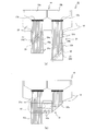
- FIG. 1 is a view showing a main part of a manufacturing process of a single-layer COF (Chip 0n Film) type driver chip module according to the first embodiment
- FIG. 1 (b) is a view showing a completed view thereof.
- the single-layer COF type driver chip module 15 of this example includes a single-layer flexible board 16 and a plurality of (examples shown in FIG. 1) mounted on the single-layer flexible board 16. 2) semiconductor chips 17 (17a, 17b).
- the output wiring 18 on the output side 18 (19a, 19b) is printed on the single-layer flexible substrate 16 described above.
- the inner ends of the individual output side connection wirings of the output side connection wiring part 19 are respectively connected to the output side of the semiconductor chip 17 (17a, 17b).
- two substrate individual extending portions 22 (22 a and 22 b) that are separately drawn out are formed.
- the input side connection wiring portions 24 (24a, 24b) are printed and wired continuously to the main body portion 23 on which the semiconductor chip 17 of the single-layer flexible substrate 16 is mounted and the individual substrate extension portion 22.
- each input side connection wiring 31 (31a, 31b) of the input side connection wiring section 24 is connected to the input side of the semiconductor chip 17 (17a, 17b).
- a resist material coating surface 25 is formed on the entire surface of the single-layer flexible substrate 16 from the semiconductor chip 17, the output-side connection wiring portion 19, and the input-side connection wiring portion 23.
- a single-layer FPC Flexible Printed Circuits
- a reel material can be adopted, so that the above configuration can be easily realized by an operation with an automatic bonding machine.
- one input side connection wiring part 22 as a reference for example, the input side connection wiring part 22a
- another input side connection wiring part 22 FIG. 1A
- the input-side connecting wiring portion 22b has the individual substrate extending portion bent by about 90 ° with the resist material coating surface 25 inside.
- an overlapping portion 26 is formed in a state where the tip end portion is overlapped with the resist material coating surface 25 of the input side connection wiring portion 22a as a reference.
- the input side connection wirings of the input side connection wiring portions 22a and 22b are individually connected in the portion corresponding to the overlapping portion 26 described above.
- the resist material removing portion 28 from which the resist material on the resist material coating surface 25 has been removed is formed in the opposing portion 27.
- ACF is an electrically conductive adhesive having anisotropic conductivity that retains insulation in the plane direction and conductivity in the thickness direction.
- the conductive adhesive 29 is attached to the resist material removal portions 28 of both the input side connection wiring portions 22a and 22b in order to show the attachment position of the conductive adhesive 29.
- the resist material removal portions 28 of both the input side connection wiring portions 22a and 22b are attached to show the attachment position of the conductive adhesive 29.
- only one of them is sufficient.
- each input side connection wiring 31 (31a, 31b) of each of the input side connection wiring portions 22 (22a, 22b) individually corresponds.
- the opposite portions are electrically connected via the conductive adhesive 29.
- the single-layer flexible substrate 16 includes a driver chip module including two output side connection wiring portions 19a and 19b and one input side connection wiring portion 22a as a reference. Form. That is, the single layer COF type driver chip module 15 is completed.
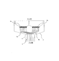
- FIG. 2 is a diagram showing a modification of the first embodiment.
- the same components and functional parts as those shown in FIGS. 1A and 1B are assigned the same reference numerals as those in FIGS. 1A and 1B.
- the printed wiring of the input side connection wiring portion 22b is formed at a finer pitch than in the case of FIGS. 1 (a) and 1 (b).
- the width of the individual board extending portion 22b on which the input side connecting wiring portion 22b is arranged is narrowed according to the minute printed wiring. As a result, as shown in FIG. 2, when the individual board extending portion 22b is bent by 90 °, the width of the portion overlapping the reference individual board extending portion 22a is narrowed. Thus, there is an effect that the single-layer COF type driver chip module 30 can be miniaturized.
- FIG. 3 is a plan view showing a configuration of a single layer COF type driver chip module according to the second embodiment.
- the same components and functions as those shown in FIGS. 1 (a) and 1 (b) are given the same numbers as those in FIGS. 1 (a) and 1 (b).
- the single-layer COF type driver chip module 31 shown in FIG. 3 has three semiconductor chips 17 (17a, 17b, 17c) mounted on the single-layer flexible substrate 16. Corresponding to the three semiconductor chips 17, three output side connection wiring portions 19 (19 a, 19 b, 19 c) are printed on the output side 18.
- the input side connection wiring part 24 (24a, 24b, 24c) is printed wiring continuously from the main body part 23 on which the semiconductor chip 17 of the single-layer flexible substrate 16 is mounted and the board individual extension part 22. Has been.
- each input side connection wiring 31 (31a, 31b, 31c) of the input side connection wiring section 24 is connected to the input side of the semiconductor chip 17 (17a, 17b, 17c), respectively.
- a resist material coating surface 25 is formed on the entire surface of the single-layer flexible substrate 16 from the semiconductor chip 17, the output connection wiring portion 19, and the input connection wiring portion 23.
- one input side connection wiring portion 22b among the three input side connection wiring portions 22 is used as a reference.
- another input side connection wiring portion 22c is bent to the right by 90 ° with the resist material coating surface 25 inside and the input side connection wiring portion 22c. It overlaps with the part 22b.
- the other input side connection wiring portion 22a is bent by 90 ° to the left with the resist material coating surface 25 inside, and the overlapping portion of the input side connection wiring portions 22b and 22c. At the position shifted in the direction of the input side 21 that does not overlap with the input side 26, the input side connection wiring portion 22b is overlaid.
- a resist material removing portion 28 is provided in a portion 27 where each input-side connection wiring is individually opposed in advance.
- a conductive adhesive 29 is formed and attached.
- each input side connection wiring 31 (31a, 31b, 31c) of each of the input side connection wiring portions 22 (22a, 22b, 22c). ) are electrically connected via the conductive adhesive 29 at the portions corresponding to each other.
- the single-layer flexible substrate 16 forms a driver chip module including three output side connection wiring portions 19a, 19b, and 19c and a reference input side connection wiring portion 22b. That is, the single layer COF type driver chip module 31 is completed.
- the present invention is not limited to this, and when four or more semiconductor chips 17 are mounted.
- the input side connection wiring part 22 can be comprised by one piece.
- the present invention can be used for a single layer COF type driver chip module in which the input wiring sides of a plurality of single layer COF type driver chips are integrated without using a two layer FPC.
Landscapes
- Engineering & Computer Science (AREA)
- Microelectronics & Electronic Packaging (AREA)
- Structure Of Printed Boards (AREA)
- Combinations Of Printed Boards (AREA)
Abstract
複数個の単層COF型ドライバチップの入力配線側を2層FPCを用いずに一体化した単層COF型ドライバチップモジュールを提供する。単層フレキシブル基板16にそれぞれ2個の出力側接続配線部19と入力側接続配線部24がプリント配線され、2個の半導体チップ17が実装され、レジスト材被膜面25が形成される。2つの入力側接続配線部24は、本体部23から個別に分かれて引き出されて形成されている基板個別延出部22にプリント配線されている。入力側接続配線部24bはレジスト材被膜面25を内側にして基板個別延出部22bを90°折り曲げられ、その先端部は入力側接続配線部24aのレジスト材被膜面25との重ね合わせ部26を形成する。重ね合わせ部26の接続配線31の対向部分27には予めレジスト材除去部28が形成され、導電性接着剤29が貼着され、表裏からの押圧により接続配線31が接続されて一体化している。
Description
本発明は、単層COF(Chip 0n Film)型ドライバチップモジュールに係わり、更に詳しくは液晶パネル等の表示パネルに実装される駆動装置としての複数個の単層COF型ドライバチップの入力配線側を2層FPCを用いずに一体化して表示パネル等の制御基板に実装可能な形態にした単層COF型ドライバチップモジュールに関する。
従来、2つのドライバチップが1つのフレキシブル基板に実装され、その2つのドライバチップに形成された入力端子に接続される配線の一部が共用化されているCOF型ドライバチップモジュールが提案されている(例えば、特許文献1参照)。
また、フレキシブル基板に2つのドライバが実装され、各入力配線がゲート電極の配列方向に複数並設され、各ドライバごとに入力配線を有しているCOF型ドライバチップモジュールが提案されている(例えば、特許文献2参照)。
ところで、従来、COF型としてフレキシブル基板に2個のドライバチップを実装した場合、それらの入力配線部を1個の入力端子部に纏めるためには、パターンの関係上、2層のFPC(Flexible Printed Circuits)を使用しなければならなかった。
図4は、従来の2個のドライバの入力配線部を1個のコネクタ接続用入力端子部に纏めるために2層FPCを使用しなければならない1例を示す図である。同図は、2層FPC1に2個のドライバ2(2a、2b)が実装されている。そして、それぞれの入力配線部3(3a、3b)が、接続部4で入力配線1本ごとに相互に接続されて、1個の入力端子部5を形成している。
図5は、従来の2個のドライバの入力配線部を1個のコネクタ接続用入力端子部に纏めるために2層FPCを使用しなければならない他の例を示す図である。同図は、2個の単層FPC6にそれぞれ実装されたドライバ2(2a、2b)の入力配線部7及び7を、1個の入力コネクタ8に接続するために、入力配線部7及び7と入力コネクタ8との間に2層FPC9を介在させている。
この2層FPC9には、図4に示した入力配線部3(3a、3b)、接続部4、及び入力端子部5と同様な、入力配線部11(11a、11b)、接続部12、及び入力端子部13が形成されている。なお、入力コネクタ8は制御基板14のコネクタであり、制御基板14は例えば液晶パネル等の制御基板である。
図6は、従来の2個のドライバを2層のFPCを使用しないでコネクタに接続する場合の例を示す図である。この場合は2個のドライバは、それぞれ単独でその入力配線部7をコネクタ8に接続することになるので、ドライバそのものは単層FPC6に実装することができる。しかし、制御基板14の方に入力コネクタ8が2個必要となり、制御基板14がコスト高を招くことになる。
上記のように、従来は、2個のドライバの入力配線部を1個のコネクタ接続用入力端子部に纏めるためには、2層FPCを用いなければならない。しかし、2層FPCは単層FPCよりも高価である。
そればかりでなく、2層FPCはリール材が存在しない。そのためドライバチップを実装する際に自動ボンディング機を使用することができない。したがって、個別の実装作業となるため、材料的にも作業的にも高コストであるという課題がある。
そうかといって、2層FPCを使用しないで2個のドライバの入力配線部をコネクタに接続しようとすると、コネクタが2個必要となって制御基板側のコストが増加する。
本発明は、上記従来の課題を解決するものであって、複数個の単層COF型ドライバチップの入力配線側を2層FPCを用いずに一体化して表示パネル等の制御基板に実装可能な形態にした単層COF型ドライバチップモジュールを提供することを目的とする。
本発明は、上記従来の課題を解決するものであって、複数個の単層COF型ドライバチップの入力配線側を2層FPCを用いずに一体化して表示パネル等の制御基板に実装可能な形態にした単層COF型ドライバチップモジュールを提供することを目的とする。
上記課題を解決するために、本発明の単層COF型ドライバチップモジュールは、単層フレキシブル基板と、該単層フレキシブル基板に実装された複数の半導体チップと、複数の上記半導体チップにそれぞれ接続され、上記単層フレキシブル基板にプリント配線されてレジスト材で被膜された複数の出力側接続配線部と、複数の上記半導体チップにそれぞれ接続され、上記単層フレキシブル基板の個別に分かれて引き出されて形成されている複数の基板個別延出部にプリント配線されてレジスト材で被膜された複数の入力側接続配線部と、を有し、複数の上記入力側接続配線部のうち、基準とする1つの上記入力側接続配線部に対し、他の上記入力側接続配線部は上記レジスト材で被膜された面を内側にして上記基板個別延出部を折り曲げられ、その先端部を基準とする1つの上記入力側接続配線部の上記レジスト材で被膜された面に重ね合わせた状態の重ね合わせ部を形成し、該重ね合わせ部において、それぞれの上記入力側接続配線部の個々の入力側接続配線が個々に対応して対向する部分の上記レジスト材が予め除去されたレジスト材除去部を形成しており、該レジスト材除去部には導電性接着剤が予め介装されており、該導電性接着剤を介して、それぞれの上記入力側接続配線部の個々の入力側接続配線が個々に対応して対向する部分で電気的に接続されていることにより、上記単層フレキシブル基板は複数の上記出力側接続配線部と、基準とする1つの上記入力側接続配線部とからなるドライバチップモジュールを形成する、ように構成される。
本発明は、複数個のCOF型ドライバチップの入力配線側を2層FPCを用いずに一体化できるので、ドライバチップを単層FPCに実装することができ、これにより、ドライバチップモジュールを安価な単層FPCで実現可能となるだけでなく、単層FPCであればリール材を採用できるので自動ボンディング機での作業が可能となって作業コストを抑えることができ、部品コストと作業コストの両面で製作費用を低減させることができるという効果を奏する。
以下、本発明の実施の形態について、詳細に説明する。
図1は、実施例1に係る単層COF(Chip 0n Film)型ドライバチップモジュールの製造過程の要部を示す図であり、図1(b)はその完成図を示す図である。図1(a),(b)に示すように、本例の単層COF型ドライバチップモジュール15は、単層フレキシブル基板16と、その単層フレキシブル基板16に実装された複数(図1の例では2個)の半導体チップ17(17a、17b)を備えている。
上記の単層フレキシブル基板16には、出力側18に出力側接続配線部19(19a、19b)がプリント配線されている。出力側接続配線部19の個々の出力側接続配線の内側端部は、それぞれ半導体チップ17(17a、17b)の出力側に接続されている。
また、単層フレキシブル基板16の入力側21には、個別に分かれて引き出された2つの基板個別延出部22(22a、22b)が形成されている。単層フレキシブル基板16の半導体チップ17が実装されている本体部23と基板個別延出部22とに連続して、入力側接続配線部24(24a、24b)がプリント配線されている。
入力側接続配線部24の個々の入力側接続配線31(31a、31b)の内側端部は、それぞれ半導体チップ17(17a、17b)の入力側に接続されている。これらの半導体チップ17、出力側接続配線部19、及び入力側接続配線部23が配設されている上から、単層フレキシブル基板16の全面に、レジスト材被膜面25が形成されている。
上記の単層フレキシブル基板16には、例えば単層FPC(Flexible Printed Circuits)を用いることができる。単層FPCであれば、リール材を採用できるので自動ボンディング機での作業で上記の構成を容易に実現することができる。
次に、上記2つの入力側接続配線部22のうち基準とする1つの入力側接続配線部22、例えば入力側接続配線部22aに対し、他の入力側接続配線部22(図1(a),(b)の場合は入力側接続配線部22b)は、図1(b)に示すように、レジスト材被膜面25を内側にして基板個別延出部をほぼ90°折り曲げられる。そして、その先端部を、基準とする入力側接続配線部22aのレジスト材被膜面25に重ね合わせた状態の重ね合わせ部26が形成される。
この折り曲げと重ね合わせに先立って、図1(a)に示すように、上記の重ね合わせ部26に対応する部分において、入力側接続配線部22a及び22bそれぞれの個々の入力側接続配線が個々に対応して対向する部分27に、レジスト材被膜面25のレジスト材が除去されたレジスト材除去部28が形成される。
そして、このレジスト材除去部28には導電性接着剤29が予め貼着される。なお、導電性接着剤29としては、ACF(Anisotropic Conductive Film)を用いる。ACFは面方向に絶縁性を保持し、厚み方向に導電性を持つ異方性の導電性を持つ導電性接着剤である。
また、図1(a)では、導電性接着剤29の貼着位置を示すため、入力側接続配線部22a及び22b双方のレジスト材除去部28に導電性接着剤29を貼着したように示しているが、実際には、いずれか一方のみでよい。
こののち、図1(b)に示すように、入力側接続配線部22bをレジスト材被膜面25を内側にして基板個別延出部22bをほぼ90°折り曲げると、図1(a)に示す入力側接続配線部22a及び22bのレジスト材除去部28が導電性接着剤29を介して重ね合わせられる。
ここで、重ね合わせ部26を表裏から押圧装置を用いて押圧すれば、入力側接続配線部22(22a、22b)それぞれの個々の入力側接続配線31(31a、31b)が個々に対応して対向する部分で、導電性接着剤29を介して、電気的に接続される。
これにより、図1(b)に示すように、単層フレキシブル基板16は、2つの出力側接続配線部19a、19bと、基準とする1つの入力側接続配線部22aとからなるドライバチップモジュールを形成する。すなわち、単層COF型ドライバチップモジュール15が完成する。
図2は、実施例1の変形例を示す図である。なお、図2には、図1(a),(b)に示した構成と同一の構成及び機能部分には図1(a),(b)と同一の番号を付与して示している。図2に示す単層COF型ドライバチップモジュール30は、入力側接続配線部22bのプリント配線が図1(a),(b)の場合よりも細かいピッチで形成されている。
プリント配線が細かい分に応じて、入力側接続配線部22bが配設されている基板個別延出部22bの幅が細く形成されている。これにより、図2に示すように、基板個別延出部22bを90°折り曲げたとき、基準の基板個別延出部22aと重なる部分の幅が狭くなるので、その狭くなった分だけ入力側21の端子を短くできる、つまり単層COF型ドライバチップモジュール30を小型化できるという効果がある。
図3は、実施例2に係る単層COF型ドライバチップモジュールの構成を示す平面図である。なお、図3には図1(a),(b)に示した構成と同一の構成及び機能部分には図1(a),(b)と同一の番号を付与して示している。
図3示す単層COF型ドライバチップモジュール31は、単層フレキシブル基板16に、3個の半導体チップ17(17a、17b、17c)が実装されている。この3個の半導体チップ17に対応して、出力側18には、3つの出力側接続配線部19(19a、19b、19c)がプリント配線されている。
各出力側接続配線部19の個々の出力側接続配線の内側端部が、それぞれ半導体チップ17(17a、17b、17c)の出力側に接続されていることは、図1の場合と同様である。
また、単層フレキシブル基板16の入力側21には、3個の半導体チップ17に対応して、3つの基板個別延出部22(22a、22b、22c)が形成されている。この場合も、単層フレキシブル基板16の半導体チップ17が実装されている本体部23と基板個別延出部22とに連続して、入力側接続配線部24(24a、24b、24c)がプリント配線されている。
入力側接続配線部24の個々の入力側接続配線31(31a、31b、31c)の内側端部は、それぞれ半導体チップ17(17a、17b、17c)の入力側に接続されている。
これらの半導体チップ17、出力側接続配線部19、及び入力側接続配線部23が配設されている上から、単層フレキシブル基板16の全面に、レジスト材被膜面25が形成されている。
ここで、上記3つの入力側接続配線部22のうち1つの入力側接続配線部22bを基準とすることにする。この入力側接続配線部22bに対し、他の1つの入力側接続配線部22cを、レジスト材被膜面25を内側にして基板個別延出部22cを90°右方に折り曲げて、入力側接続配線部22bに重ねる。
他のもう1つの入力側接続配線部22aを、レジスト材被膜面25を内側にして基板個別延出部22aを90°左方に折り曲げて、入力側接続配線部22bと22cとの重ね合わせ部26に重複しない入力側21方向にずれた位置で、入力側接続配線部22bに重ねる。
いずれの重ね合わせ部26においても、折り曲げと重ね合わせに先立って、図1の場合と同様に、予め個々の入力側接続配線が個々に対応して対向する部分27に、レジスト材除去部28が形成され、導電性接着剤29が貼着されている。
この場合も、2つの重ね合わせ部26を表裏から押圧装置を用いて押圧すれば、入力側接続配線部22(22a、22b、22c)それぞれの個々の入力側接続配線31(31a、31b、31c)が個々に対応して対向する部分で、導電性接着剤29を介して、電気的に接続される。
これにより、図3に示すように、単層フレキシブル基板16は、3つの出力側接続配線部19a、19b、19cと、基準の入力側接続配線部22bとからなるドライバチップモジュールを形成する。すなわち、単層COF型ドライバチップモジュール31が完成する。
なお、上記の実施例では単層フレキシブル基板16に実装された半導体チップ17が2個の場合と3個の場合を示したが、これに限ることなく、半導体チップ17を4個以上実装した場合でも、図3に示す手法を用いれば、入力側接続配線部22を1個で構成することができる。
本発明は、複数個の単層COF型ドライバチップの入力配線側を2層FPCを用いずに一体化した単層COF型ドライバチップモジュールに利用することができる。
1 2層FPC
2(2a、2b) ドライバ
3(3a、3b) 入力配線部
4 接続部
5 入力端子部
6 単層FPC
7 入力配線部
8 入力コネクタ
9 2層FPC
11(11a、11b) 入力配線部
12 接続部
13 入力端子部
14 制御基板
15 単層COF型ドライバチップモジュール
16 単層フレキシブル基板
17(17a、17b) 半導体チップ
18 出力側
19(19a、19b) 出力側接続配線部
21 入力側
22(22a、22b) 基板個別延出部
23 本体部
24(24a、24b) 入力側接続配線部
25 レジスト材被膜面
26 重ね合わせ部
27 対向部分
28 レジスト材除去部
29 導電性接着剤
30、31 単層COF型ドライバチップモジュール
2(2a、2b) ドライバ
3(3a、3b) 入力配線部
4 接続部
5 入力端子部
6 単層FPC
7 入力配線部
8 入力コネクタ
9 2層FPC
11(11a、11b) 入力配線部
12 接続部
13 入力端子部
14 制御基板
15 単層COF型ドライバチップモジュール
16 単層フレキシブル基板
17(17a、17b) 半導体チップ
18 出力側
19(19a、19b) 出力側接続配線部
21 入力側
22(22a、22b) 基板個別延出部
23 本体部
24(24a、24b) 入力側接続配線部
25 レジスト材被膜面
26 重ね合わせ部
27 対向部分
28 レジスト材除去部
29 導電性接着剤
30、31 単層COF型ドライバチップモジュール
Claims (3)
- 単層フレキシブル基板と、
該単層フレキシブル基板に実装された複数の半導体チップと、
複数の前記半導体チップにそれぞれ接続され、前記単層フレキシブル基板にプリント配線されてレジスト材で被膜された複数の出力側接続配線部と、
複数の前記半導体チップにそれぞれ接続され、前記単層フレキシブル基板の個別に分かれて引き出されて形成されている複数の基板個別延出部にプリント配線されてレジスト材で被膜された複数の入力側接続配線部と、
を有し、
複数の前記入力側接続配線部のうち、基準とする1つの前記入力側接続配線部に対し、他の前記入力側接続配線部は前記レジスト材で被膜された面を内側にして前記基板個別延出部を折り曲げられ、その先端部を基準とする1つの前記入力側接続配線部の前記レジスト材で被膜された面に重ね合わせた状態の重ね合わせ部を形成し、
該重ね合わせ部において、それぞれの前記入力側接続配線部の個々の入力側接続配線が個々に対応して対向する部分の前記レジスト材が予め除去されたレジスト材除去部を形成しており、
該レジスト材除去部には導電性接着剤が予め介装されており、
該導電性接着剤を介して、それぞれの前記入力側接続配線部の個々の入力側接続配線が個々に対応して対向する部分で電気的に接続されていることにより、
前記単層フレキシブル基板は複数の前記出力側接続配線部と、基準とする1つの前記入力側接続配線部とからなるドライバチップモジュールを形成する、
ことを特徴とする単層COF(Chip 0n Film)型ドライバチップモジュール。 - 前記導電性接着剤は、ACF(Anisotropic Conductive Film)である、ことを特徴とする請求項1に記載の単層COF(Chip 0n Film)型ドライバチップモジュール。
- 前記単層フレキシブル基板は、単層FPC(Flexible Printed Circuits)である、ことを特徴とする請求項1または2に記載の単層COF(Chip 0n Film)型ドライバチップモジュール。
Priority Applications (2)
| Application Number | Priority Date | Filing Date | Title |
|---|---|---|---|
| PCT/JP2011/051966 WO2012104979A1 (ja) | 2011-01-31 | 2011-01-31 | 単層COF(Chip 0n Film)型ドライバチップモジュール |
| TW100148870A TW201236126A (en) | 2011-01-31 | 2011-12-27 | Single-layer chip-on-film (cof) type driver chip module |
Applications Claiming Priority (1)
| Application Number | Priority Date | Filing Date | Title |
|---|---|---|---|
| PCT/JP2011/051966 WO2012104979A1 (ja) | 2011-01-31 | 2011-01-31 | 単層COF(Chip 0n Film)型ドライバチップモジュール |
Publications (1)
| Publication Number | Publication Date |
|---|---|
| WO2012104979A1 true WO2012104979A1 (ja) | 2012-08-09 |
Family
ID=46602224
Family Applications (1)
| Application Number | Title | Priority Date | Filing Date |
|---|---|---|---|
| PCT/JP2011/051966 Ceased WO2012104979A1 (ja) | 2011-01-31 | 2011-01-31 | 単層COF(Chip 0n Film)型ドライバチップモジュール |
Country Status (2)
| Country | Link |
|---|---|
| TW (1) | TW201236126A (ja) |
| WO (1) | WO2012104979A1 (ja) |
Citations (3)
| Publication number | Priority date | Publication date | Assignee | Title |
|---|---|---|---|---|
| JPH0426180A (ja) * | 1990-05-22 | 1992-01-29 | Nec Corp | フレキシブル配線フイルム |
| JPH0448676A (ja) * | 1990-06-14 | 1992-02-18 | Hitachi Chem Co Ltd | フレキシブル印刷配線板 |
| JPH0831477A (ja) * | 1994-07-11 | 1996-02-02 | Kiyousera Elco Kk | Fpc基板、及び該fpc基板と基板の接続装置 |
-
2011
- 2011-01-31 WO PCT/JP2011/051966 patent/WO2012104979A1/ja not_active Ceased
- 2011-12-27 TW TW100148870A patent/TW201236126A/zh unknown
Patent Citations (3)
| Publication number | Priority date | Publication date | Assignee | Title |
|---|---|---|---|---|
| JPH0426180A (ja) * | 1990-05-22 | 1992-01-29 | Nec Corp | フレキシブル配線フイルム |
| JPH0448676A (ja) * | 1990-06-14 | 1992-02-18 | Hitachi Chem Co Ltd | フレキシブル印刷配線板 |
| JPH0831477A (ja) * | 1994-07-11 | 1996-02-02 | Kiyousera Elco Kk | Fpc基板、及び該fpc基板と基板の接続装置 |
Also Published As
| Publication number | Publication date |
|---|---|
| TW201236126A (en) | 2012-09-01 |
Similar Documents
| Publication | Publication Date | Title |
|---|---|---|
| JP6528272B2 (ja) | 接続用基板および表示装置 | |
| CN102113421B (zh) | 柔性基板和电路构造体 | |
| TWI476738B (zh) | 軟性顯示面板及其組裝方法 | |
| JP4938239B2 (ja) | 表示装置 | |
| US20110169792A1 (en) | Display panel | |
| US7349054B2 (en) | Method of mounting flexible circuit boards, and display device | |
| CN113178132A (zh) | 覆晶薄膜组、显示面板及显示模组 | |
| CN102834855B (zh) | 显示装置 | |
| US7420821B2 (en) | Electronic module and driving circuit board therefor | |
| KR101842065B1 (ko) | 연성 회로 기판 | |
| CN101238759A (zh) | 电路部件、电极连接构造以及具备它们的显示装置 | |
| JPH0422075A (ja) | 配線接続装置 | |
| JP2002141620A (ja) | フレキシブル配線基板 | |
| JPH09203907A (ja) | 液晶表示装置及びその製造装置 | |
| JP2004109969A (ja) | 液晶表示装置 | |
| JP5091513B2 (ja) | 液晶表示装置 | |
| WO2012104979A1 (ja) | 単層COF(Chip 0n Film)型ドライバチップモジュール | |
| JP2017167208A (ja) | 表示装置 | |
| WO2016158747A1 (ja) | 部品実装用フレキシブル基板および表示装置 | |
| JP2008216466A (ja) | 表示装置およびその製造方法 | |
| JP4874612B2 (ja) | 液晶表示モジュール | |
| JP2009016578A (ja) | フレキシブル配線基板、該フレキシブル配線基板を用いた半導体装置、および該半導体装置を備えた表示装置 | |
| JP2002236458A (ja) | 表示装置の実装構造 | |
| KR20000071304A (ko) | 저비용 테이프캐리어패키지 및 그를 이용한 액정모듈 | |
| JP2017195216A (ja) | 回路基板、集積回路付き回路基板および回路基板の製造方法 |
Legal Events
| Date | Code | Title | Description |
|---|---|---|---|
| 121 | Ep: the epo has been informed by wipo that ep was designated in this application |
Ref document number: 11857677 Country of ref document: EP Kind code of ref document: A1 |
|
| NENP | Non-entry into the national phase |
Ref country code: DE |
|
| 122 | Ep: pct application non-entry in european phase |
Ref document number: 11857677 Country of ref document: EP Kind code of ref document: A1 |
|
| NENP | Non-entry into the national phase |
Ref country code: JP |