WO2012099012A1 - 坩堝および蒸着装置 - Google Patents
坩堝および蒸着装置 Download PDFInfo
- Publication number
- WO2012099012A1 WO2012099012A1 PCT/JP2012/050581 JP2012050581W WO2012099012A1 WO 2012099012 A1 WO2012099012 A1 WO 2012099012A1 JP 2012050581 W JP2012050581 W JP 2012050581W WO 2012099012 A1 WO2012099012 A1 WO 2012099012A1
- Authority
- WO
- WIPO (PCT)
- Prior art keywords
- vapor deposition
- crucible
- substrate
- reflecting member
- target substrate
- Prior art date
- Legal status (The legal status is an assumption and is not a legal conclusion. Google has not performed a legal analysis and makes no representation as to the accuracy of the status listed.)
- Ceased
Links
Images






Classifications
-
- C—CHEMISTRY; METALLURGY
- C23—COATING METALLIC MATERIAL; COATING MATERIAL WITH METALLIC MATERIAL; CHEMICAL SURFACE TREATMENT; DIFFUSION TREATMENT OF METALLIC MATERIAL; COATING BY VACUUM EVAPORATION, BY SPUTTERING, BY ION IMPLANTATION OR BY CHEMICAL VAPOUR DEPOSITION, IN GENERAL; INHIBITING CORROSION OF METALLIC MATERIAL OR INCRUSTATION IN GENERAL
- C23C—COATING METALLIC MATERIAL; COATING MATERIAL WITH METALLIC MATERIAL; SURFACE TREATMENT OF METALLIC MATERIAL BY DIFFUSION INTO THE SURFACE, BY CHEMICAL CONVERSION OR SUBSTITUTION; COATING BY VACUUM EVAPORATION, BY SPUTTERING, BY ION IMPLANTATION OR BY CHEMICAL VAPOUR DEPOSITION, IN GENERAL
- C23C16/00—Chemical coating by decomposition of gaseous compounds, without leaving reaction products of surface material in the coating, i.e. chemical vapour deposition [CVD] processes
- C23C16/44—Chemical coating by decomposition of gaseous compounds, without leaving reaction products of surface material in the coating, i.e. chemical vapour deposition [CVD] processes characterised by the method of coating
- C23C16/448—Chemical coating by decomposition of gaseous compounds, without leaving reaction products of surface material in the coating, i.e. chemical vapour deposition [CVD] processes characterised by the method of coating characterised by the method used for generating reactive gas streams, e.g. by evaporation or sublimation of precursor materials
-
- C—CHEMISTRY; METALLURGY
- C23—COATING METALLIC MATERIAL; COATING MATERIAL WITH METALLIC MATERIAL; CHEMICAL SURFACE TREATMENT; DIFFUSION TREATMENT OF METALLIC MATERIAL; COATING BY VACUUM EVAPORATION, BY SPUTTERING, BY ION IMPLANTATION OR BY CHEMICAL VAPOUR DEPOSITION, IN GENERAL; INHIBITING CORROSION OF METALLIC MATERIAL OR INCRUSTATION IN GENERAL
- C23C—COATING METALLIC MATERIAL; COATING MATERIAL WITH METALLIC MATERIAL; SURFACE TREATMENT OF METALLIC MATERIAL BY DIFFUSION INTO THE SURFACE, BY CHEMICAL CONVERSION OR SUBSTITUTION; COATING BY VACUUM EVAPORATION, BY SPUTTERING, BY ION IMPLANTATION OR BY CHEMICAL VAPOUR DEPOSITION, IN GENERAL
- C23C14/00—Coating by vacuum evaporation, by sputtering or by ion implantation of the coating forming material
- C23C14/22—Coating by vacuum evaporation, by sputtering or by ion implantation of the coating forming material characterised by the process of coating
- C23C14/24—Vacuum evaporation
- C23C14/243—Crucibles for source material
-
- C—CHEMISTRY; METALLURGY
- C23—COATING METALLIC MATERIAL; COATING MATERIAL WITH METALLIC MATERIAL; CHEMICAL SURFACE TREATMENT; DIFFUSION TREATMENT OF METALLIC MATERIAL; COATING BY VACUUM EVAPORATION, BY SPUTTERING, BY ION IMPLANTATION OR BY CHEMICAL VAPOUR DEPOSITION, IN GENERAL; INHIBITING CORROSION OF METALLIC MATERIAL OR INCRUSTATION IN GENERAL
- C23C—COATING METALLIC MATERIAL; COATING MATERIAL WITH METALLIC MATERIAL; SURFACE TREATMENT OF METALLIC MATERIAL BY DIFFUSION INTO THE SURFACE, BY CHEMICAL CONVERSION OR SUBSTITUTION; COATING BY VACUUM EVAPORATION, BY SPUTTERING, BY ION IMPLANTATION OR BY CHEMICAL VAPOUR DEPOSITION, IN GENERAL
- C23C16/00—Chemical coating by decomposition of gaseous compounds, without leaving reaction products of surface material in the coating, i.e. chemical vapour deposition [CVD] processes
- C23C16/04—Coating on selected surface areas, e.g. using masks
- C23C16/042—Coating on selected surface areas, e.g. using masks using masks
-
- G—PHYSICS
- G03—PHOTOGRAPHY; CINEMATOGRAPHY; ANALOGOUS TECHNIQUES USING WAVES OTHER THAN OPTICAL WAVES; ELECTROGRAPHY; HOLOGRAPHY
- G03B—APPARATUS OR ARRANGEMENTS FOR TAKING PHOTOGRAPHS OR FOR PROJECTING OR VIEWING THEM; APPARATUS OR ARRANGEMENTS EMPLOYING ANALOGOUS TECHNIQUES USING WAVES OTHER THAN OPTICAL WAVES; ACCESSORIES THEREFOR
- G03B37/00—Panoramic or wide-screen photography; Photographing extended surfaces, e.g. for surveying; Photographing internal surfaces, e.g. of pipe
- G03B37/06—Panoramic or wide-screen photography; Photographing extended surfaces, e.g. for surveying; Photographing internal surfaces, e.g. of pipe involving anamorphosis
-
- H—ELECTRICITY
- H10—SEMICONDUCTOR DEVICES; ELECTRIC SOLID-STATE DEVICES NOT OTHERWISE PROVIDED FOR
- H10K—ORGANIC ELECTRIC SOLID-STATE DEVICES
- H10K71/00—Manufacture or treatment specially adapted for the organic devices covered by this subclass
- H10K71/10—Deposition of organic active material
- H10K71/16—Deposition of organic active material using physical vapour deposition [PVD], e.g. vacuum deposition or sputtering
Definitions
- the present invention relates to a crucible and a vapor deposition apparatus for depositing a pattern of vapor deposition particles on a film formation substrate.
- flat panel displays have been used in various products and fields, and further flat panel displays are required to have larger sizes, higher image quality, and lower power consumption.
- an organic EL display device including an organic EL element using electroluminescence (hereinafter referred to as “EL”) of an organic material is an all-solid-state type, low voltage driving, high speed response, As a flat panel display excellent in terms of self-luminous property and the like, it is attracting a great deal of attention.
- the organic EL display device has, for example, a configuration in which an organic EL element connected to a TFT is provided on a substrate made of a glass substrate or the like provided with a TFT (thin film transistor).
- the organic EL element is a light emitting element that can emit light with high luminance by low-voltage direct current drive, and has a structure in which a first electrode, an organic EL layer, and a second electrode are stacked in this order. Of these, the first electrode is connected to the TFT. In addition, between the first electrode and the second electrode, as the organic EL layer, a hole injection layer, a hole transport layer, an electron blocking layer, a light emitting layer, a hole blocking layer, an electron transport layer, an electron injection layer The organic layer which laminated
- organic EL elements including light emitting layers of red (R), green (G), and blue (B) are arranged and formed on a substrate as sub-pixels. A color image is displayed by selectively emitting light from these organic EL elements with a desired luminance using TFTs.
- an organic EL display device In order to manufacture an organic EL display device, it is necessary to form a light emitting layer made of an organic light emitting material that emits light of each color in a predetermined pattern for each organic EL element. In addition, for a layer that does not require pattern formation for each organic EL element, a thin film is collectively formed on the entire pixel region constituted by the organic EL element.
- a vacuum deposition method for example, a vacuum deposition method, an ink jet method, and a laser transfer method are known.
- a vacuum deposition method is often used.
- a mask also referred to as a shadow mask in which openings having a predetermined pattern are formed is used.
- the deposition surface of the substrate to which the mask is closely fixed is opposed to the deposition source.
- vapor deposition particles film forming material from the vapor deposition source are vapor deposited on the vapor deposition surface through the opening of the mask, thereby forming a thin film having a predetermined pattern.
- Vapor deposition is performed for each color of the light emitting layer (this is called “separate vapor deposition”).
- Patent Document 1 discloses a technique for allowing a vapor deposition material to efficiently reach a substrate to be processed and bringing the vapor deposition material to a state where the vapor deposition material is perpendicularly incident on the substrate to be processed. Yes.
- FIG. 15 is a cross-sectional view showing the configuration of the vapor deposition apparatus 100 described in Patent Document 1.
- a substrate holder 119 that holds the substrate to be processed 120 and the mask 131 is disposed at an upper position in the vapor deposition chamber 111, and vapor deposition particles are directed toward the substrate to be processed 120 at a lower position in the vapor deposition chamber 111.
- the vapor deposition source 112 to be supplied is arranged.
- the mask 131 is overlaid at a predetermined position on the lower surface side (film formation surface side) of the substrate 120 to be processed.
- the evaporation source 112 includes an evaporation crucible 140 loaded with an evaporation material.
- the crucible 140 is disposed immediately below the center of the substrate to be processed 120, and vapor deposition is performed with the substrate to be processed 120 fixed.
- the crucible 140 includes a heating container 141 loaded with a vapor deposition material, a vapor flow outlet 143a that ejects a vapor flow, and a cylindrical guide member 142 that surrounds the vapor flow discharge path and opens in the vapor flow discharge direction. And.
- a steam flow outlet 143a is disposed at the focal point of the flight direction control concave curved surface 142d formed of a paraboloid that reflects the colliding vapor deposition particles in the emission direction.
- the vapor deposition material heated in the heating container 141 is discharged as a vapor flow from the vapor flow outlet 143a and is deposited on the substrate 120 to be processed.
- the discharge path of the steam flow is surrounded by the concave curved surface 142d for flight direction control.
- the vapor deposition particles flying obliquely to the side are reflected by the flying direction control concave curved surface 142d and travel toward the substrate 120 to be processed.
- the vapor flow is directed toward the substrate 120 to be processed with a small divergence angle, it is possible to prevent the vapor deposition particles from adhering to the inner wall of the vapor deposition chamber 111, so that the vapor deposition material can efficiently reach the substrate 120 to be processed. Can do. In addition, it is possible to approach the state in which the vapor deposition particles are perpendicularly incident on the substrate 120 to be processed.
- the mask and the frame for holding it become huge and its weight increases, which makes it difficult to handle and may hinder productivity and safety.
- the vapor deposition apparatus and its accompanying apparatus are similarly enlarged and complicated, the apparatus design becomes difficult and the installation cost becomes high.
- a shadow mask smaller than the substrate is used, the deposition source and the shadow mask are integrated, and the gap between the shadow mask and the substrate is kept constant, either the integrated product or the substrate.
- a method of forming an organic film pattern on the position of a predetermined substrate can be considered by performing vapor deposition while scanning.
- a vapor deposition apparatus using the scan vapor deposition method will be described with reference to FIGS.
- FIG. 16 is a cross-sectional view showing a configuration of a vapor deposition apparatus 200 using a scan vapor deposition method.
- the vapor deposition apparatus 200 is an apparatus that deposits vapor deposition particles on the deposition target substrate 210, and includes a mask 220, a limiting plate 230, a shutter 240, and a crucible 250.
- the deposition target substrate 210, the mask 220, the limiting plate 230, and the shutter 240 are supported by the frame 260, and the crucible 250 is placed on the support base 270.
- the deposition target substrate 210 is supported by the movable support portion 261 of the frame 260.
- the movable support portion 261 can be moved in the X-axis direction (the front side in the drawing) by a drive system including a stepping motor, a roller, a gear, and the like.
- a drive system including a stepping motor, a roller, a gear, and the like.
- the mask 220 and the limiting plate 230 are supported by the fixed support portions 262 and 263 of the frame 260, respectively.
- the shutter 240 is supported by the movable support portion 264 of the frame 260.
- the movable support portion 264 can be moved in the X-axis direction by the drive system, similarly to the movable support portion 261.
- the driving system drives the movable support portion 264, the shutter 240 moves in the X-axis direction.
- Each component of the vapor deposition apparatus 200 is accommodated in the chamber 280. Further, the inside of the chamber 280 is in a vacuum state by the vacuum pump mechanism 281.
- a plurality of crucibles 250 are arranged in a direction (Y-axis direction) perpendicular to the moving direction of the deposition target substrate 210, and include a heater 251 and a container 252.
- the container 252 stores a solid or liquid vapor deposition material.
- the heater 251 heats the container 252
- the vapor deposition material is vaporized into gas vapor deposition particles.
- the vapor deposition particles are ejected from the opening 253 of the crucible 250 toward the deposition target substrate 210.
- FIG. 17 is a perspective view showing the arrangement of the film formation substrate 210, the mask 220, the limiting plate 230, the shutter 240, and the crucible 250.
- members that support the deposition target substrate 210, the mask 220, the limiting plate 230, the shutter 240, and the crucible 250 are omitted.
- the deposition target substrate 210 is moved (scanned) in the X-axis direction during vapor deposition.
- the mask 220 and the limiting plate 230 are fixed.
- the vapor deposition particles injected from the opening 253 of the crucible 250 reach the deposition target substrate 210 through the opening 231 of the limiting plate 230 and the opening 221 of the mask 220.
- the vapor deposition particles are ejected radially with a certain extent, but the spread of the vapor deposition particles is suppressed by passing through the opening 231 of the limiting plate 230.
- a plurality of openings 221 of the mask 220 are formed at a predetermined interval.
- a plurality of stripe-shaped film formation patterns are formed on the film formation substrate 210.
- the shutter 240 is used as necessary in order to control the arrival of vapor deposition particles to the film formation substrate 210.
- the shutter 240 is moved between the crucible 250 and the limiting plate 230 when the deposition unnecessary region of the deposition target substrate 210 passes over the mask 220. As a result, the vapor deposition particles do not reach the deposition target substrate 210, so that vapor deposition on the vapor deposition unnecessary region can be prevented.
- the deposition target substrate 210 and the mask 220 are separated (so-called gap vapor deposition method). Therefore, when the flow of vapor deposition particles (vapor deposition flow) has a component in the oblique direction with respect to the normal direction of the film formation surface of the film formation substrate 210, it passes through the mask 220 and reaches the film formation substrate 210.
- the angle of the deposition flow is oblique. In that case, there is a possibility that the film formation pattern is blurred or the film formation position is shifted. As a result, there arises a problem that the production yield is lowered and a high-definition organic EL panel cannot be formed.
- the vapor deposition flow injected from the vapor flow outlet 143a is collimated (parallelized) to some extent, but the end of the substrate 120 to be processed. Increasing toward the portion, the light is incident obliquely with respect to the normal direction of the film formation surface. That is, the vapor deposition stream is not fully collimated.
- Patent Document 1 when the technique of Patent Document 1 is applied to the vapor deposition apparatus 200 using the scan vapor deposition method, a high-definition film pattern can be obtained unless a sufficiently thick restriction plate 230 is used to collimate the vapor deposition flow. I can't. However, when the thickness of the restriction plate 230 is increased, the number of vapor deposition particles adhering to the wall surface of the opening 231 of the restriction plate 230 increases, and the utilization efficiency of the vapor deposition particles is reduced.
- the present invention has been made to solve the above-described problems, and an object thereof is to realize a crucible and a vapor deposition apparatus capable of forming a film with high accuracy.
- a crucible according to the present invention is a crucible including an opening for injecting vapor deposition particles to a deposition target substrate, provided at a position facing the opening, and the opening A first reflecting member that reflects the vapor deposition particles emitted from the first reflective member; and a second reflective member that reflects the vapor deposition particles reflected by the first reflective member toward the deposition target substrate.
- a first reflecting member that reflects the vapor deposition particles emitted from the first reflective member
- a second reflective member that reflects the vapor deposition particles reflected by the first reflective member toward the deposition target substrate.
- the vapor deposition particles emitted from the opening are reflected by the first reflecting member, and then reflected by the second reflecting member toward the deposition target substrate. Since the first reflecting member is provided at a position facing the opening, and the second reflecting member has a concave curved surface with respect to the deposition target substrate, the vapor deposition particles reflected by the second reflecting member are not formed. It flows in a state parallel or nearly parallel to the normal direction of the film substrate. Therefore, it is possible to form a good vapor deposition film with little pattern abnormality such as blurring or misalignment of the film formation pattern. Therefore, a crucible capable of highly accurate film formation can be realized.
- the vapor deposition apparatus according to the present invention is characterized by including the above-described crucible.
- the crucible according to the present invention is a crucible including an opening for injecting vapor deposition particles to a deposition target substrate, provided at a position facing the opening, and injected from the opening.
- the vapor deposition apparatus which concerns on this invention is equipped with the crucible which concerns on this invention. Therefore, there is an effect that a crucible and a vapor deposition apparatus capable of highly accurate film formation can be realized.
- (A)-(c) is sectional drawing which shows an example of the horizontal support
- FIG. 17 is a perspective view showing an arrangement of a film formation substrate, a mask, a limiting plate, a shutter, and a crucible in the vapor deposition apparatus shown in FIG. 16.
- FIG. 1 is a cross-sectional view showing a configuration of a vapor deposition apparatus 1 according to the present embodiment.
- the vapor deposition apparatus 1 is an apparatus that deposits vapor deposition particles on the deposition target substrate 10 and includes a mask 20, a shutter 40, and a crucible 50.
- the deposition target substrate 10, the mask 20, and the shutter 40 are supported by a frame 60, and the crucible 50 is placed on a support base 70.
- the deposition target substrate 10 is supported by the movable support portion 61 of the frame 60.
- the movable support 61 can be moved in the X-axis direction (the front side of the drawing) by a drive system including a stepping motor, a roller, a gear, and the like.
- a drive system including a stepping motor, a roller, a gear, and the like.
- the mask 20 is supported by the fixed support portion 63 of the frame 60. An opening corresponding to a pattern to be formed on the deposition target substrate 10 is formed in the mask 20. Note that the mask 20 may not be provided when a solid pattern is formed on the deposition target substrate 10.
- the shutter 40 is supported by the movable support portion 64 of the frame 60.
- the movable support portion 64 can be moved in the X-axis direction by the drive system, similarly to the movable support portion 61.
- the drive system drives the movable support portion 64
- the shutter 40 moves in the X-axis direction.
- the shutter 40 is moved from the influence range of the vapor deposition flow only during vapor deposition.
- Each component of the vapor deposition apparatus 1 is accommodated in the chamber 80. Further, the inside of the chamber 80 is in a vacuum state by the vacuum pump mechanism 81.
- a plurality of crucibles 50 are arranged along a direction (Y-axis direction) perpendicular to both the relative movement direction (X-axis direction) of the deposition target substrate 10 and the normal direction (Z-axis direction) of the deposition target substrate 10.
- the heater 51 and the container 52 are provided.
- the container 52 stores a solid or liquid vapor deposition material. When the heater 51 heats the container 52, the vapor deposition material is vaporized to become vapor deposited particles. Thereby, the vapor deposition particles are ejected from the crucible 50 toward the deposition target substrate 10.
- Each member other than the crucible 50 of the vapor deposition apparatus 1 is the same as that in the vapor deposition apparatus 200 shown in FIG. That is, the vapor deposition apparatus 1 has a configuration in which the crucible 250 is replaced with the crucible 50 and the limiting plate 230 is omitted in the vapor deposition apparatus 200.
- vapor deposition particles from the crucible 50 are incident on the deposition target substrate 10 almost perpendicularly. That is, a vapor deposition flow substantially parallel to the normal direction of the deposition target substrate 10 is ejected from the crucible 50. Therefore, there is no need to provide a limiting plate for collimating the vapor deposition flow.
- a configuration for injecting parallel vapor deposition flows will be described with reference to FIGS.
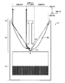
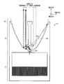
- FIG. 2 is an enlarged cross-sectional view showing the configuration of the container 52 of the crucible 50
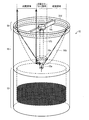
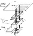
- FIG. 3 is an enlarged perspective view showing the configuration of the container 52
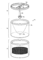
- FIG. 4 is an exploded perspective view showing the configuration of the container 52. .
- the container 52 includes a vapor deposition source unit 53, a first reflecting member unit 54, and a second reflecting member unit 55. These three members are joined by, for example, screw machining. Moreover, it is desirable that the temperature of each member can be adjusted independently.
- the vapor deposition source unit 53 is a cylindrical container for storing vapor deposition material.
- the first reflecting member unit 54 includes a focusing member 54a, a vertical column 54b, a horizontal column 54c, and an annular support 54d.
- the horizontal strut 54c is formed so as to pass through the central portion of the annular support portion 54d and connect two locations on the inner peripheral portion.
- One end of the vertical column 54b is connected to the midpoint of the horizontal column 54c and extends downward.
- the other end of the vertical column 54b is connected to the focal member 54a.
- the focusing member 54a corresponds to the first reflecting member described in the claims.
- the second reflecting member unit 55 is a cylindrical member having an opening 55a and a paraboloid 55b formed therein.
- the paraboloid 55b corresponds to the second reflecting member recited in the claims, and has a parabolic shape that is recessed with respect to the deposition target substrate 10.
- the opening 55a is formed in a region including the apex of the paraboloid 55b.
- the annular support portion 54 d of the first reflecting member unit 54 is placed on the outer periphery of the upper end of the second reflecting member unit 55.
- the focal member 54a is supported at a position facing the opening 55a (directly above the opening 55a). More specifically, the focal member 54a is supported at a position including the focal point of the paraboloid 55b.
- the focus member 54a is formed in a conical shape having a vertex on the opening 55a side.
- At least the focal member 54a is kept at a temperature higher than the sublimation temperature or evaporation temperature (that is, the vaporization temperature) of the vapor deposition particles. Further, the surface of the rotating paraboloid 55b is also maintained at a temperature higher than the vaporization temperature of the vapor deposition particles.
- the vapor deposition particles emitted from the opening 55a are completely elastically reflected by the focal member 54a toward the paraboloid 55b.
- the focal member 54a is supported at a position including the focal point of the rotating parabolic surface 55b, the traveling direction of the vapor deposition particles reflected by the focal member 54a and further reflected by the rotating parabolic surface 55b is parabolic. According to the principle, it is almost perpendicular to the deposition target substrate 10. That is, a vapor deposition flow substantially parallel to the normal direction of the deposition target substrate 10 is ejected from the crucible 50.
- the traveling direction of the vapor deposition particles reflected by the rotary paraboloid 55b is relative to the normal direction of the deposition target substrate 10. If they are completely parallel to each other, the vapor deposition particles do not reach the region facing the focal member 54a on the deposition target substrate 10. Therefore, the region is a region where no film is formed. However, in the case of scanning vapor deposition, there is no problem because vapor deposition is performed while the film formation target substrate 10 is relatively moved.
- the focal member 54a and the rotating paraboloid 55b are preferably formed of a material that has high thermal conductivity and can be uniformly heated in order to reflect the vapor deposition particles completely elastically.
- the material of the focal member 54a and the rotating paraboloid 55b simple substances such as aluminum nitride, silicon carbide, copper, gold, silver, molybdenum, nickel, and alloys thereof can be used.
- the surfaces of the focal member 54a and the rotating paraboloid 55b may be formed of a plating film made of the above material.
- FIG. 5 is a diagram for explaining the parabolic principle.
- the focal member 54 a is formed so that the vapor deposition particles emitted from the opening 55 a do not directly radiate in the direction of the deposition target substrate 10. That is, by forming the maximum diameter of the focal member 54a sufficiently larger than the diameter of the opening 55a, all the vapor deposition particles emitted from the opening 55a are reflected by the focal member 54a. Further, the position of the focal member 54a is preferably close to the bottom of the paraboloid 55b.
- the focal member 54a is small, it is known that the opening 55a is clogged when the vapor deposition material is deposited. Therefore, the practical size of the focusing member 54a is preferably 0.5 mm to 10 mm. When the size of the focal member 54a increases, the parallelism of the vapor deposition flow decreases. However, by reducing the size of the paraboloid 55b sufficiently larger than the size of the focal member 54a, it is possible to suppress the decrease in parallelism. In the present embodiment, the diameter of the opening 55a is 2 mm. The maximum diameter of the paraboloid 55b is 50 mm.
- a straight line (a broken line arrow in FIG. 2) connecting the end of the maximum diameter portion of the focal member 54a and the portion closest to the end on the outer periphery of the opening 55a intersects the paraboloid 55b.
- the focal member 54a is formed.
- a straight line connecting an arbitrary part on the outer periphery of the opening 55a and a part closest to the arbitrary part among the parts closest to the film formation substrate 10 of the paraboloid 55b is a focal member 54a.
- the focal member 54a is formed so as to intersect with. Thereby, it is possible to prevent the vapor deposition particles not reflected by the focal member 54a from reaching the film formation substrate 10 without colliding with the paraboloid 55b.
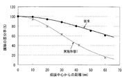
- FIG. 6 is a graph showing the film thickness distribution of vapor deposition particles in the conventional crucible and the crucible according to the present embodiment.
- the thick line indicates the film thickness distribution of the vapor deposition particles in the conventional crucible
- the thin line indicates the film thickness distribution of the vapor deposition particles in the crucible according to the present embodiment.
- a crucible having an opening with a diameter of 2 mm and a length of 25 mm was used as the crucible.
- an alkali-free glass substrate was used as a film formation substrate, and Alq3 was used as a vapor deposition material.
- the distance between the alkali-free glass substrate and the opening was 125 mm, the film formation rate was 0.1 nm / sec, and the degree of vacuum in the chamber was 10 ⁇ 3 Pa or less.
- a film was formed on an alkali-free glass substrate so that the central film thickness was 100 nm, and the film thickness distribution on the substrate was measured in percentage with the central film thickness as 100%.
- the film thickness distribution indicated by the broken line has a greater degree of decrease in film thickness with respect to the distance from the film formation center than the film thickness distribution indicated by the solid line. That is, the crucible according to the present embodiment injects the vapor deposition particles more parallel to the normal direction of the deposition target substrate than the conventional crucible.
- the N value is a value that quantitatively indicates the film formation state (scattering / diffusion state in the chamber) unique to the material.
- the derivation of the N value will be described.
- the vapor deposition rate R sp ( ⁇ ) on the spherical surface having the radius L 0 is expressed by the following equation, where the vapor deposition rate directly above the vapor deposition source is R 0 .
- the deposition amount per unit time (deposition rate) R ( ⁇ ) on the substrate at an angle ⁇ with respect to the direction directly above the deposition source is:
- the performance of the vapor deposition source itself is an N value.
- the component “+3” is a geometric component.
- the conventional crucible has an N value of 1.5
- the crucible according to the present embodiment has an N value of 14.0.
- the shape of the horizontal support 54c shown in FIGS. 3 and 4 will be described. It is preferable that the cross section of the horizontal support 54c has a shape elongated in the traveling direction of the vapor deposition flow so that the vapor deposition flow is not affected. On the other hand, it is necessary to form a horizontal thickness of the horizontal column 54c so that the temperature is transmitted to the focus member 54a.
- FIGS. 10A to 10C are cross-sectional views showing an example of the horizontal support 54c.
- the cross section of the horizontal support column 54c is elongated in the vertical direction (the direction in which the vapor deposition flow proceeds).
- the horizontal width is 1 mm and the vertical width is 5 mm.
- the cross-sectional shapes shown in FIGS. 10B and 10C are tapered downward.
- the vapor deposition particles flow from the bottom to the top of the drawing, in the example shown in FIGS. 10A and 10B, the vapor deposition particles are reflected on the bottom surface of the horizontal column 54c to cut the vapor deposition particles toward the deposition target substrate. Therefore, the film formation efficiency is lowered.
- the vapor deposition particles are hardly reflected on the horizontal support column 54c, so that it is possible to suppress a decrease in film formation efficiency. Therefore, among the forms shown in FIGS. 10A to 10C, the form shown in FIG. 10C is the most desirable.
- the limiting plate for collimating the vapor deposition flow is not provided, but a limiting plate may be provided when a minute oblique component of the vapor deposition particles becomes a problem. Even in the case where the limiting plate is provided, the vapor deposition flow is substantially parallel to the normal direction of the deposition target substrate, so that the vapor deposition particles hardly adhere to the limiting plate.
- FIG. 11 is a cross-sectional view showing the configuration of the crucible container 52 ′ according to the present embodiment.
- the container 52 ' has a configuration in which the first reflecting member unit 54 is replaced with the first reflecting member unit 54' in the container 52 shown in FIG.
- the first reflecting member unit 54 ' is configured by replacing the focusing member 54a with the focusing member 54a' in the first reflecting member unit 54.
- the focus member 54a according to the first embodiment has a conical shape
- the focus member 54a 'according to the present embodiment has a flat plate shape. Therefore, the vapor deposition particles injected from the opening 55a are repelled toward the vapor deposition source unit 53 to some extent.
- the amount of vapor deposition particles released is reduced, and the film formation rate is likely to be lowered.
- the focus member 54a ' has a simpler shape than the focus member 54a, the apparatus cost can be reduced.
- a straight line (broken line arrow in FIG. 11) connecting the end of the maximum diameter portion of the focal member 54a ′ and the portion closest to the end on the outer periphery of the opening 55a intersects with the paraboloid 55b.
- a focal member 54a ' is formed. For this reason, also in this embodiment, collimation of a vapor deposition flow is possible to some extent.
- FIG. 12 is a graph showing the film thickness distribution of vapor deposition particles in the conventional crucible and the crucible according to the present embodiment.
- the thick line indicates the film thickness distribution of the vapor deposition particles in the conventional crucible
- the thin line indicates the film thickness distribution of the vapor deposition particles in the crucible according to the present embodiment.
- Measurement conditions such as the crucible, the film formation substrate, and the evaporation material used are the same as those in the first embodiment.
- the conventional crucible has an N value of 1.5, whereas the crucible according to the present embodiment has an N value of 7.6. That is, also in the crucible according to the present embodiment, unnecessary spread of the vapor deposition film on the deposition target substrate can be suppressed.
- FIG. 13 is a cross-sectional view showing the structure of the crucible container 52 ′′ according to the present embodiment.
- the container 52 ′′ is the same as the second reflecting member unit 55 ′ in the container 52 shown in FIG. The configuration is replaced with.
- the second reflecting member unit 55 ′ has a configuration in which a cylindrical extension 55 c is further provided in the second reflecting member unit 55.
- the cylindrical extension 55c is a cylindrical member that extends from the outer periphery of the opening 55a toward the focal member 54a. That is, the end of the cylindrical extension portion 55 c becomes an injection port for vapor deposition particles supplied from the vapor deposition source unit 53.
- the cylindrical extension portion 55c can be formed by Ni-coating a cylinder cut from a pure copper member.
- the structure of the apparatus is slightly more complicated than that of the first embodiment, but the focal region can be further narrowed because the injection port of the vapor deposition particles is closer to the focal member 54a. For this reason, the traveling direction of the vapor deposition particles reflected by the focal member 54 a and the rotating paraboloid 55 b can be made more parallel to the normal direction of the deposition target substrate 10.
- a straight line (broken arrow in FIG. 13) connecting the end of the maximum diameter portion of the focal member 54a and the portion closest to the end on the outer periphery of the cylindrical extension 55c intersects the paraboloid 55b.
- FIG. 14 is a graph showing the film thickness distribution of vapor deposition particles in a conventional crucible and a crucible according to the present embodiment.
- the thick line indicates the film thickness distribution of the vapor deposition particles in the conventional crucible
- the thin line indicates the film thickness distribution of the vapor deposition particles in the crucible according to the present embodiment.
- the measurement conditions such as the crucible, the film formation substrate, and the vapor deposition material used are the same as those in the first and second embodiments.
- the conventional crucible has an N value of 1.5, whereas the crucible according to this embodiment has an N value of 20.5. That is, in the crucible according to the present embodiment, a practically sufficient N value is obtained.
- each of the second reflecting members has a parabolic shape.
- the second reflecting member does not have to be completely parabolic, and may be a concave curved surface close to a parabolic shape.
- Vapor deposition may be performed without relative movement.
- a structure in which a plurality of crucibles are provided at a position facing the deposition film forming surface of the deposition target substrate may be used, or the crucibles may be arranged in a row or in a matrix.
- vapor deposition may be performed using one or a few crucibles.
- a plurality of crucibles are arranged along a direction perpendicular to both the relative movement direction of the deposition target substrate and the normal direction of the deposition target substrate. It may be slightly deviated from the direction perpendicular to the scanning direction of the film formation substrate.
- the concave curved surface is a rotary paraboloid and the first reflecting member is located at a focal point of the rotary paraboloid.
- the traveling direction of the vapor deposition particles reflected by the second reflecting member can be made substantially parallel to the normal direction of the deposition target substrate.
- a straight line connecting an arbitrary portion on the outer periphery of the opening and a portion closest to the arbitrary portion of the concave curved surface closest to the deposition target substrate is formed. It is preferable that the first reflecting member intersects the first reflecting member.
- the size of the first reflecting member is small, a part of the vapor deposition particles from the opening may reach the deposition target substrate without being reflected by the first reflecting member.
- the first reflecting member is formed in a conical shape having a vertex on the opening side.
- the vapor deposition particles reflected by the first reflecting member almost face the second reflecting member and do not return to the opening, so that the film forming rate and productivity can be improved.
- the first reflecting member is formed in a flat plate shape facing the opening.
- the shape of the first reflecting member is simple, the apparatus cost can be reduced.
- the crucible includes a cylindrical extension extending from the outer periphery of the opening to the first reflecting member side.
- the focal region can be further narrowed down. For this reason, the advancing direction of the vapor deposition particles reflected by the first reflecting member and the second reflecting member can be made more parallel to the normal direction of the film formation substrate.
- the temperature of the first reflecting member is preferably equal to or higher than the vaporization temperature of the vapor deposition particles.
- the vapor deposition particles adhere to the first reflection member, and it becomes difficult to make the vapor deposition flow parallel.
- the vapor deposition particles collide completely with the first reflecting member and are reflected at the same angle as the incident angle to the collision surface of the first reflecting member. Can be easily achieved.
- the temperature of the second reflecting member is preferably equal to or higher than the vaporization temperature of the vapor deposition particles.
- the vapor deposition particles adhere to the second reflection member, and it becomes difficult to make the vapor deposition flow parallel.
- the vapor deposition particles collide with the second reflecting member completely and are reflected at the same angle as the incident angle to the collision surface of the first reflecting member. Can be easily achieved.
- the vapor deposition apparatus includes any one of the above crucibles.
- a plurality of the crucibles are provided at positions facing the vapor deposition film forming surface of the deposition target substrate.
- a vapor deposition mask for forming a vapor deposition film pattern on the film formation substrate is provided between the second reflective member of the crucible and the film formation substrate. It is preferable.
- the vapor deposition mask for forming a vapor deposition film pattern on the film formation substrate between the second reflective member of the crucible and the film formation substrate, and the vapor deposition It is preferable to include a limiting plate for bringing the traveling direction of the particles closer to the normal direction of the deposition target substrate.
- the traveling direction of the vapor deposition particles reflected by the second reflecting member further approaches the normal direction of the film formation substrate, so that the vapor deposition flow can be further collimated.
- the vapor deposition apparatus further includes a moving unit that moves the deposition target substrate relative to the crucible.
- the deposition substrate is large, when forming a deposition film with the deposition substrate stationary, a deposition source area that is almost the same size as the deposition substrate is required, and a large number of crucibles are required. Thus, there is a problem that the device cost increases.
- the deposition target substrate is conveyed in-line and vapor deposition is performed, so that the number of crucibles can be reduced. Thereby, apparatus cost can be reduced.
- a plurality of the crucibles are arranged along a direction perpendicular to both the relative movement direction of the deposition target substrate and the normal direction of the deposition target substrate. Is preferred.
- the alignment between the crucible and the deposition target substrate becomes easy. Further, the vapor deposition apparatus can be reduced in size.
- the present invention can be applied not only to vapor deposition of vapor deposition particles in the manufacture of an organic EL display device but also to vapor deposition of vapor deposition particles to any film formation target.
- Vapor deposition apparatus 10 Film-forming substrate 20
- Mask vapor deposition mask
- shutter 50 crucible 51 heater 52 container 52 ′ container 52 ”container
- deposition source unit 54 first reflecting member unit 54 ′ first reflecting member unit
- focusing member 54a ′ focusing member
- 54b vertical column
- 54c horizontal column
- second reflecting member unit 55 ′
- Second reflecting member unit 55a Opening 55b Paraboloid 55c
- Cylindrical extension 60
- Fixed support 64 Movable support 70 Support base 80 Chamber 81 Vacuum pump mechanism
Landscapes
- Chemical & Material Sciences (AREA)
- Chemical Kinetics & Catalysis (AREA)
- Engineering & Computer Science (AREA)
- Materials Engineering (AREA)
- Mechanical Engineering (AREA)
- Metallurgy (AREA)
- Organic Chemistry (AREA)
- General Chemical & Material Sciences (AREA)
- Physical Vapour Deposition (AREA)
- Electroluminescent Light Sources (AREA)
Abstract
Description
本発明の第1の実施形態について図1~図10に基づいて説明すれば、以下のとおりである。




本発明の第2の実施形態について図11および図12に基づいて説明すれば、以下のとおりである。なお、説明の便宜上、前記実施形態1にて説明した部材と同じ機能を有する部材については、同じ符号を付記し、その説明を省略する。
本発明の第3の実施形態について図13および図14に基づいて説明すれば、以下のとおりである。なお、説明の便宜上、前記実施形態1にて説明した部材と同じ機能を有する部材については、同じ符号を付記し、その説明を省略する。
上記では、第2反射部材がいずれもパラボラ形状を有していたが、完全にパラボラ形状である必要はなく、パラボラ形状に近い凹曲面であってもよい。
以上のように、本発明の実施形態に係る坩堝では、前記凹曲面は、回転放物面であり、前記第1反射部材は、前記回転放物面の焦点に位置することが好ましい。
10 被成膜基板
20 マスク(蒸着マスク)
40 シャッタ
50 坩堝
51 加熱ヒータ
52 容器
52’ 容器
52” 容器
53 蒸着源ユニット
54 第1反射部材ユニット
54’ 第1反射部材ユニット
54a 焦点部材
54a’ 焦点部材
54b 鉛直支柱
54c 水平支柱
54d 環状支持部
55 第2反射部材ユニット
55’ 第2反射部材ユニット
55a 開口部
55b 回転放物面
55c 筒状延長部
60 フレーム
61 可動支持部
63 固定支持部
64 可動支持部
70 支持台
80 チャンバ
81 真空ポンプ機構
Claims (14)
- 被成膜基板に対し蒸着粒子を射出する開口部を備える坩堝であって、
前記開口部に対向する位置に設けられ、前記開口部から射出された蒸着粒子を反射する第1反射部材と、
前記第1反射部材によって反射された蒸着粒子を前記被成膜基板に向けて反射する第2反射部材とを備え、
前記第2反射部材は、前記被成膜基板に対して凹曲面を有していることを特徴とする坩堝。 - 請求項1に記載の坩堝において、
前記凹曲面は、回転放物面であり、
前記第1反射部材は、前記回転放物面の焦点に位置することを特徴とする坩堝。 - 請求項1または2に記載の坩堝において、
前記開口部の外周上の任意の部分と、前記凹曲面の前記被成膜基板に最も近い部分のうち前記任意の部分に最も近い部分とを結ぶ直線が、前記第1反射部材と交差することを特徴とする坩堝。 - 請求項1~3のいずれか1項に記載の坩堝において、
前記第1反射部材は、前記開口部側に頂点を有する円錐形状に形成されていることを特徴とする坩堝。 - 請求項1~3のいずれか1項に記載の坩堝において、
前記第1反射部材は、前記開口部に対向する平板形状に形成されていることを特徴とする坩堝。 - 請求項1~5のいずれか1項に記載の坩堝において、
前記開口部の外周から前記第1反射部材側に延びる筒状延長部を備えることを特徴とする坩堝。 - 請求項1~6のいずれか1項に記載の坩堝において、
前記第1反射部材の温度は前記蒸着粒子の気化温度以上であることを特徴とする坩堝。 - 請求項1~7のいずれか1項に記載の坩堝において、
前記第2反射部材の温度は前記蒸着粒子の気化温度以上であることを特徴とする坩堝。 - 請求項1~8のいずれか1項に記載の坩堝を備えることを特徴とする蒸着装置。
- 請求項9に記載の蒸着装置において、
前記被成膜基板の蒸着膜形成面と対向する位置に、前記坩堝を複数備えることを特徴とする蒸着装置。 - 請求項9または10に記載の蒸着装置において、
前記坩堝の第2反射部材と前記被成膜基板との間に、前記被成膜基板に蒸着膜のパターンを形成するための蒸着マスクを備えていることを特徴とする蒸着装置。 - 請求項9または10に記載の蒸着装置において、
前記坩堝の第2反射部材と前記被成膜基板との間に、
前記被成膜基板に蒸着膜のパターンを形成するための蒸着マスクと、
前記蒸着粒子の進行方向を前記被成膜基板の法線方向に近づけるための制限板とを備えていることを特徴とする蒸着装置。 - 請求項9~12のいずれか1項に記載の蒸着装置において、
前記坩堝に対して前記被成膜基板を相対移動させる移動手段を備えることを特徴とする蒸着装置。 - 請求項13に記載の蒸着装置において、
前記坩堝は、前記被成膜基板の相対移動方向と前記被成膜基板の法線方向との両方に垂直な方向に沿って複数配置されていることを特徴とする蒸着装置。
Priority Applications (3)
| Application Number | Priority Date | Filing Date | Title |
|---|---|---|---|
| CN201280005720.6A CN103328681B (zh) | 2011-01-20 | 2012-01-13 | 坩埚和蒸镀装置 |
| JP2012553682A JP5319025B2 (ja) | 2011-01-20 | 2012-01-13 | 坩堝および蒸着装置 |
| US13/980,875 US8673082B2 (en) | 2011-01-20 | 2012-01-13 | Crucible and deposition apparatus |
Applications Claiming Priority (2)
| Application Number | Priority Date | Filing Date | Title |
|---|---|---|---|
| JP2011010174 | 2011-01-20 | ||
| JP2011-010174 | 2011-01-20 |
Publications (1)
| Publication Number | Publication Date |
|---|---|
| WO2012099012A1 true WO2012099012A1 (ja) | 2012-07-26 |
Family
ID=46515640
Family Applications (1)
| Application Number | Title | Priority Date | Filing Date |
|---|---|---|---|
| PCT/JP2012/050581 Ceased WO2012099012A1 (ja) | 2011-01-20 | 2012-01-13 | 坩堝および蒸着装置 |
Country Status (4)
| Country | Link |
|---|---|
| US (1) | US8673082B2 (ja) |
| JP (1) | JP5319025B2 (ja) |
| CN (1) | CN103328681B (ja) |
| WO (1) | WO2012099012A1 (ja) |
Cited By (5)
| Publication number | Priority date | Publication date | Assignee | Title |
|---|---|---|---|---|
| US20140037849A1 (en) * | 2012-07-31 | 2014-02-06 | Sung-Joong Joo | Depositing apparatus and method for measuring deposition quantity using the same |
| CN103849857A (zh) * | 2012-12-03 | 2014-06-11 | 三星显示有限公司 | 薄膜沉积源、沉积装置和使用该沉积装置的沉积方法 |
| JP2017014616A (ja) * | 2015-06-26 | 2017-01-19 | キヤノントッキ株式会社 | 蒸着装置 |
| JP2020176284A (ja) * | 2019-04-16 | 2020-10-29 | 株式会社アルバック | 蒸着源、真空処理装置、及び成膜方法 |
| JP2025009986A (ja) * | 2023-06-29 | 2025-01-20 | 安徽熙泰智能科技有限公司 | 薄膜沈着装置およびその沈着方法 |
Families Citing this family (26)
| Publication number | Priority date | Publication date | Assignee | Title |
|---|---|---|---|---|
| JP5328726B2 (ja) | 2009-08-25 | 2013-10-30 | 三星ディスプレイ株式會社 | 薄膜蒸着装置及びこれを利用した有機発光ディスプレイ装置の製造方法 |
| JP5677785B2 (ja) | 2009-08-27 | 2015-02-25 | 三星ディスプレイ株式會社Samsung Display Co.,Ltd. | 薄膜蒸着装置及びこれを利用した有機発光表示装置の製造方法 |
| US8876975B2 (en) * | 2009-10-19 | 2014-11-04 | Samsung Display Co., Ltd. | Thin film deposition apparatus |
| KR101084184B1 (ko) | 2010-01-11 | 2011-11-17 | 삼성모바일디스플레이주식회사 | 박막 증착 장치 |
| KR101193186B1 (ko) | 2010-02-01 | 2012-10-19 | 삼성디스플레이 주식회사 | 박막 증착 장치, 이를 이용한 유기 발광 디스플레이 장치의 제조방법 및 이에 따라 제조된 유기 발광 디스플레이 장치 |
| KR101156441B1 (ko) | 2010-03-11 | 2012-06-18 | 삼성모바일디스플레이주식회사 | 박막 증착 장치 |
| US8894458B2 (en) | 2010-04-28 | 2014-11-25 | Samsung Display Co., Ltd. | Thin film deposition apparatus, method of manufacturing organic light-emitting display device by using the apparatus, and organic light-emitting display device manufactured by using the method |
| KR101223723B1 (ko) | 2010-07-07 | 2013-01-18 | 삼성디스플레이 주식회사 | 박막 증착 장치, 이를 이용한 유기 발광 디스플레이 장치의 제조방법 및 이에 따라 제조된 유기 발광 디스플레이 장치 |
| KR101723506B1 (ko) | 2010-10-22 | 2017-04-19 | 삼성디스플레이 주식회사 | 유기층 증착 장치 및 이를 이용한 유기 발광 디스플레이 장치의 제조 방법 |
| KR101738531B1 (ko) | 2010-10-22 | 2017-05-23 | 삼성디스플레이 주식회사 | 유기 발광 디스플레이 장치의 제조 방법 및 이에 따라 제조된 유기 발광 디스플레이 장치 |
| KR20120045865A (ko) | 2010-11-01 | 2012-05-09 | 삼성모바일디스플레이주식회사 | 유기층 증착 장치 |
| KR20120065789A (ko) | 2010-12-13 | 2012-06-21 | 삼성모바일디스플레이주식회사 | 유기층 증착 장치 |
| KR101760897B1 (ko) | 2011-01-12 | 2017-07-25 | 삼성디스플레이 주식회사 | 증착원 및 이를 구비하는 유기막 증착 장치 |
| KR101840654B1 (ko) | 2011-05-25 | 2018-03-22 | 삼성디스플레이 주식회사 | 유기층 증착 장치 및 이를 이용한 유기 발광 디스플레이 장치의 제조 방법 |
| KR101852517B1 (ko) | 2011-05-25 | 2018-04-27 | 삼성디스플레이 주식회사 | 유기층 증착 장치 및 이를 이용한 유기 발광 디스플레이 장치의 제조 방법 |
| KR101857249B1 (ko) | 2011-05-27 | 2018-05-14 | 삼성디스플레이 주식회사 | 패터닝 슬릿 시트 어셈블리, 유기막 증착 장치, 유기 발광 표시장치제조 방법 및 유기 발광 표시 장치 |
| KR101826068B1 (ko) | 2011-07-04 | 2018-02-07 | 삼성디스플레이 주식회사 | 유기층 증착 장치 |
| JP6087267B2 (ja) * | 2013-12-06 | 2017-03-01 | シャープ株式会社 | 蒸着装置、蒸着方法、及び、有機エレクトロルミネッセンス素子の製造方法 |
| WO2016138964A1 (en) * | 2015-03-03 | 2016-09-09 | Applied Materials, Inc. | Nozzle for a material source arrangement used in vacuum deposition |
| KR20170104710A (ko) * | 2016-03-07 | 2017-09-18 | 삼성디스플레이 주식회사 | 성막 장치 및 표시 장치의 제조 방법 |
| CN206396318U (zh) * | 2017-01-24 | 2017-08-11 | 京东方科技集团股份有限公司 | 一种坩埚 |
| CN107686966B (zh) * | 2017-07-31 | 2019-09-24 | 武汉华星光电半导体显示技术有限公司 | 蒸镀装置 |
| US20190032193A1 (en) * | 2017-07-31 | 2019-01-31 | Wuhan China Star Optoelectronics Semiconductor Display Technology Co., Ltd. | Vapor Deposition Device |
| CN107686969A (zh) * | 2017-08-22 | 2018-02-13 | 武汉华星光电半导体显示技术有限公司 | 一种蒸发源装置 |
| CN115287623B (zh) * | 2022-08-11 | 2023-05-16 | 太原理工大学 | 一种曲面形金刚石膜片的制备方法 |
| CN116575002A (zh) * | 2023-04-11 | 2023-08-11 | 重庆金美新材料科技有限公司 | 一种改善蒸发镀膜挡板镀层的结构和真空蒸镀设备 |
Citations (4)
| Publication number | Priority date | Publication date | Assignee | Title |
|---|---|---|---|---|
| US6237529B1 (en) * | 2000-03-03 | 2001-05-29 | Eastman Kodak Company | Source for thermal physical vapor deposition of organic electroluminescent layers |
| JP2008163365A (ja) * | 2006-12-27 | 2008-07-17 | Seiko Epson Corp | 蒸着用坩堝、蒸着法および蒸着装置 |
| JP2009280861A (ja) * | 2008-05-22 | 2009-12-03 | Hitachi Zosen Corp | 真空蒸着装置の放出部構造 |
| JP2010013731A (ja) * | 2009-07-24 | 2010-01-21 | Hitachi Zosen Corp | 蒸着装置 |
Family Cites Families (6)
| Publication number | Priority date | Publication date | Assignee | Title |
|---|---|---|---|---|
| US3015013A (en) * | 1960-05-31 | 1961-12-26 | Avco Corp | High density radiant heat systems |
| US4925295A (en) * | 1986-03-17 | 1990-05-15 | Casio Computer Co., Ltd. | Projection display apparatus |
| US4787737A (en) * | 1986-03-26 | 1988-11-29 | Casio Computer Co., Ltd. | Projection display apparatus |
| US4791273A (en) * | 1987-05-15 | 1988-12-13 | Varian Associates, Inc. | Vaporizer system for ion source |
| KR100691025B1 (ko) * | 2005-12-16 | 2007-03-09 | 두산디앤디 주식회사 | 유기박막 증착용 도가니 장치 |
| WO2009034915A1 (ja) * | 2007-09-10 | 2009-03-19 | Ulvac, Inc. | 蒸着装置 |
-
2012
- 2012-01-13 US US13/980,875 patent/US8673082B2/en active Active
- 2012-01-13 CN CN201280005720.6A patent/CN103328681B/zh active Active
- 2012-01-13 WO PCT/JP2012/050581 patent/WO2012099012A1/ja not_active Ceased
- 2012-01-13 JP JP2012553682A patent/JP5319025B2/ja not_active Expired - Fee Related
Patent Citations (4)
| Publication number | Priority date | Publication date | Assignee | Title |
|---|---|---|---|---|
| US6237529B1 (en) * | 2000-03-03 | 2001-05-29 | Eastman Kodak Company | Source for thermal physical vapor deposition of organic electroluminescent layers |
| JP2008163365A (ja) * | 2006-12-27 | 2008-07-17 | Seiko Epson Corp | 蒸着用坩堝、蒸着法および蒸着装置 |
| JP2009280861A (ja) * | 2008-05-22 | 2009-12-03 | Hitachi Zosen Corp | 真空蒸着装置の放出部構造 |
| JP2010013731A (ja) * | 2009-07-24 | 2010-01-21 | Hitachi Zosen Corp | 蒸着装置 |
Cited By (10)
| Publication number | Priority date | Publication date | Assignee | Title |
|---|---|---|---|---|
| US20140037849A1 (en) * | 2012-07-31 | 2014-02-06 | Sung-Joong Joo | Depositing apparatus and method for measuring deposition quantity using the same |
| CN103572215A (zh) * | 2012-07-31 | 2014-02-12 | 三星显示有限公司 | 蒸镀装置及利用此的蒸镀量测量方法 |
| JP2014031581A (ja) * | 2012-07-31 | 2014-02-20 | Samsung Display Co Ltd | 蒸着装置およびこれを用いた蒸着量測定方法 |
| US9724715B2 (en) * | 2012-07-31 | 2017-08-08 | Samsung Display Co., Ltd | Depositing apparatus and method for measuring deposition quantity using the same |
| US20170312773A1 (en) * | 2012-07-31 | 2017-11-02 | Samsung Display Co., Ltd. | Depositing apparatus and method for measuring deposition quantity using the same |
| US10596582B2 (en) | 2012-07-31 | 2020-03-24 | Samsung Display Co., Ltd. | Depositing apparatus and method for measuring deposition quantity using the same |
| CN103849857A (zh) * | 2012-12-03 | 2014-06-11 | 三星显示有限公司 | 薄膜沉积源、沉积装置和使用该沉积装置的沉积方法 |
| JP2017014616A (ja) * | 2015-06-26 | 2017-01-19 | キヤノントッキ株式会社 | 蒸着装置 |
| JP2020176284A (ja) * | 2019-04-16 | 2020-10-29 | 株式会社アルバック | 蒸着源、真空処理装置、及び成膜方法 |
| JP2025009986A (ja) * | 2023-06-29 | 2025-01-20 | 安徽熙泰智能科技有限公司 | 薄膜沈着装置およびその沈着方法 |
Also Published As
| Publication number | Publication date |
|---|---|
| CN103328681B (zh) | 2015-09-23 |
| US8673082B2 (en) | 2014-03-18 |
| US20130291796A1 (en) | 2013-11-07 |
| CN103328681A (zh) | 2013-09-25 |
| JPWO2012099012A1 (ja) | 2014-06-09 |
| JP5319025B2 (ja) | 2013-10-16 |
Similar Documents
| Publication | Publication Date | Title |
|---|---|---|
| JP5319025B2 (ja) | 坩堝および蒸着装置 | |
| TWI598453B (zh) | 蒸鍍單元及蒸鍍裝置 | |
| JP5457548B2 (ja) | 蒸着装置及び蒸着方法 | |
| US10184167B2 (en) | Restricting plate unit, vapor deposition unit, and vapor deposition device | |
| WO2016171075A1 (ja) | 蒸着装置および蒸着方法 | |
| US20140008456A1 (en) | Deposition Apparatus | |
| CN105473757B (zh) | 蒸镀装置和有机电致发光元件的制造方法 | |
| JP2012184486A (ja) | 蒸発源および蒸着装置 | |
| WO2016136595A1 (ja) | 蒸着ユニット、蒸着装置、および蒸着方法 | |
| JPWO2019064426A1 (ja) | 蒸着源および蒸着装置並びに蒸着膜製造方法 | |
| CN111684100B (zh) | 蒸镀装置 | |
| WO2017069066A1 (ja) | スキャン蒸着用金属マスク、蒸着装置および蒸着方法およびエレクトロルミネッセンス表示装置 | |
| JP2010159454A (ja) | 成膜装置、成膜方法 | |
| KR102076843B1 (ko) | 박막 증착용 마스크 프레임 어셈블리 | |
| KR102128308B1 (ko) | Oled 디스플레이, 그 제조용 증착원과 그 제조 방법 |
Legal Events
| Date | Code | Title | Description |
|---|---|---|---|
| 121 | Ep: the epo has been informed by wipo that ep was designated in this application |
Ref document number: 12736168 Country of ref document: EP Kind code of ref document: A1 |
|
| ENP | Entry into the national phase |
Ref document number: 2012553682 Country of ref document: JP Kind code of ref document: A |
|
| WWE | Wipo information: entry into national phase |
Ref document number: 13980875 Country of ref document: US |
|
| NENP | Non-entry into the national phase |
Ref country code: DE |
|
| 122 | Ep: pct application non-entry in european phase |
Ref document number: 12736168 Country of ref document: EP Kind code of ref document: A1 |