WO2012086538A1 - 表示素子、製造方法、及び電気機器 - Google Patents
表示素子、製造方法、及び電気機器 Download PDFInfo
- Publication number
- WO2012086538A1 WO2012086538A1 PCT/JP2011/079171 JP2011079171W WO2012086538A1 WO 2012086538 A1 WO2012086538 A1 WO 2012086538A1 JP 2011079171 W JP2011079171 W JP 2011079171W WO 2012086538 A1 WO2012086538 A1 WO 2012086538A1
- Authority
- WO
- WIPO (PCT)
- Prior art keywords
- display
- polar liquid
- display element
- voltage
- electrode
- Prior art date
- Legal status (The legal status is an assumption and is not a legal conclusion. Google has not performed a legal analysis and makes no representation as to the accuracy of the status listed.)
- Ceased
Links
Images








Classifications
-
- G—PHYSICS
- G02—OPTICS
- G02B—OPTICAL ELEMENTS, SYSTEMS OR APPARATUS
- G02B26/00—Optical devices or arrangements for the control of light using movable or deformable optical elements
- G02B26/004—Optical devices or arrangements for the control of light using movable or deformable optical elements based on a displacement or a deformation of a fluid
- G02B26/005—Optical devices or arrangements for the control of light using movable or deformable optical elements based on a displacement or a deformation of a fluid based on electrowetting
Definitions
- the present invention relates to a display element that displays information such as images and characters by moving a polar liquid, a method of manufacturing the display element, and an electrical apparatus using the display element.
- a display space is formed between the first and second substrates, and ribs (partitions) are formed.
- the interior of the display space is partitioned according to a plurality of pixel regions by a wall.
- a conductive liquid (polar liquid) is sealed, and a signal electrode, a scan electrode and a reference electrode (reference electrode) provided in parallel to each other are provided. It was provided to cross.
- the conductive liquid is moved to the scan electrode side or the reference electrode side to display. The display color on the face side was changed.
- one of the first and second substrates provided with the scanning electrode and the reference electrode (reference electrode) is provided in order to increase the moving speed of the conductive liquid.
- a dielectric layer is provided on the surface on the display space side, or a water repellent film is provided on the surface of the dielectric layer and the surface on the other display space side of the first and second substrates.
- the water repellent film is provided after the rib (structure) is formed on the surface of the dielectric layer or the surface of the first and second substrates on the other display space side. It was.
- the adhesion of the water-repellent film to the rib and the dielectric layer, the first or second substrate is different, which may cause problems such as peeling of the water-repellent film.
- the conventional display element may have a problem that its reliability is lowered.
- the present invention can prevent the occurrence of defects even when the moving speed of the polar liquid is increased, and has a display element having excellent reliability, a manufacturing method thereof, and a display thereof
- An object is to provide an electrical device using the element.
- the display element according to the present invention is configured such that a predetermined display space is formed between the first substrate provided on the display surface side and the first substrate. , The second substrate provided on the non-display surface side of the first substrate, the effective display area and the non-effective display area set for the display space, and the effective inside the display space.
- a display element configured to change a display color on the display surface side by moving the polar liquid, the polar liquid being movably sealed on the display area side or the ineffective display area side
- a plurality of signal electrodes disposed in the display space so as to be in contact with the polar liquid and provided along a predetermined arrangement direction; Provided on one side of the first and second substrates in a state of being electrically insulated from the polar liquid so as to be installed on one side of the effective display area side and the non-effective display area side.
- a plurality of scanning electrodes provided to intersect with the plurality of signal electrodes, A plurality of pixel regions provided in a unit of intersection between the signal electrode and the scanning electrode; And an insulating fluid that is movably sealed for each pixel region in the display space and that does not mix with the polar liquid,
- a structure for driving the polar liquid is provided for each pixel region so as to cover the entire surface on the display space side of the substrate. It is characterized by this.
- the structure is provided on at least one side of the first and second substrates so as to cover the entire surface on the display space side of the substrate.
- a water repellent film may be formed on the surface of the structure.
- the water repellent film is formed so as to cover the surface of the structure on the display space side, and the moving speed of the polar liquid can be easily improved.
- a synthetic resin material having high water repellency having an interfacial tension of 30 mN / m or less may be used as the structure.
- the moving speed of the polar liquid can be easily improved while omitting the installation of the water repellent film.
- a synthetic resin material modified to a highly water-repellent material having an interfacial tension of 30 mN / m or less by adding a modifying agent is used as the structure. Is preferred.
- the modifier can expand options such as the kind of synthetic resin material that can constitute a structure that can easily improve the moving speed of the polar liquid while omitting the installation of the water-repellent film.
- the design freedom of the body can be expanded.
- At least one of the first and second substrates and the structure may be provided integrally.
- the structure may include a rib member provided so as to divide the inside of the display space according to the plurality of pixel regions.
- the structure may include a rail member that is provided for each of the pixel regions and constitutes a movement space for moving the insulating fluid.
- the moving speed of the polar liquid can be increased more easily.
- the signal voltage is connected to the plurality of signal electrodes, and a signal voltage within a predetermined voltage range is applied to each of the plurality of signal electrodes according to information displayed on the display surface side.
- a selection voltage that is connected to the plurality of scan electrodes and that allows the polar liquid to move within the display space in response to the signal voltage for each of the plurality of scan electrodes;
- the display color of each pixel area can be changed appropriately.
- the plurality of pixel regions may be provided in accordance with a plurality of colors capable of full color display on the display surface side.
- a color image can be displayed by appropriately moving the corresponding polar liquid in each of the plurality of pixels.
- the first liquid electrode is electrically insulated from the polar liquid and the scan electrode so as to be installed on the other side of the effective display area side and the ineffective display area side.
- a plurality of reference electrodes provided on one side of the first and second substrates and provided to intersect with the plurality of signal electrodes;
- a selection voltage that is connected to the plurality of reference electrodes and that allows the polar liquid to move within the display space in response to the signal voltage for each of the plurality of reference electrodes; It is preferable that a reference voltage application unit that applies one voltage of a non-selection voltage that prevents the polar liquid from moving inside the display space is provided.
- a dielectric layer is laminated on the surfaces of the reference electrode and the scanning electrode.
- the electric field applied to the polar liquid by the dielectric layer can be reliably increased, and the moving speed of the polar liquid can be improved more easily.
- the ineffective display area is set by a light shielding film provided on one side of the first and second substrates,
- the effective display area is preferably set by an opening formed in the light shielding film.
- the electrical device of the present invention is an electrical device including a display unit that displays information including characters and images, Any one of the display elements described above is used for the display portion.
- the first substrate is formed so that a predetermined display space is formed between the first substrate provided on the display surface side and the first substrate.
- a second substrate provided on the non-display surface side of the substrate, and an effective display area and an ineffective display area set for each of a plurality of pixel areas with respect to the display space, and the inside of the display space
- a polar liquid encapsulated movably on the effective display area side or the non-effective display area side and an insulating fluid that does not mix with the polar liquid are provided, and the display on the display surface side is displayed by moving the polar liquid.
- a method of manufacturing a display element configured to change color On at least one side of the first and second substrates, a structure for driving the polar liquid is formed for each pixel region so as to cover the entire surface of the substrate on the display space side.
- An arrangement step of arranging the material layer And an installation step of providing the structure on the surface on at least one side of the first and second substrates by performing a predetermined treatment on the material layer. It is.
- the entire surface on the display space side of the substrate is provided on at least one side of the first and second substrates by sequentially performing the arrangement step and the installation step.
- the structure can be provided so as to cover the surface.
- the structure may be provided using a predetermined mold in the installation step.
- the structure can be provided with high accuracy.
- the structure may be provided by irradiating ultraviolet rays.
- the structure can be easily provided.
- a forming step of forming a water repellent film on the surface of the structure may be performed after the installation step.
- the water repellent film is formed so as to cover the surface of the structure on the display space side, and the moving speed of the polar liquid can be easily improved.
- a synthetic resin material having high water repellency having an interfacial tension of 30 mN / m or less is used as the material layer, and at least one of the first and second substrates.
- the synthetic resin material may be disposed on one side or a predetermined mold.
- the moving speed of the polar liquid can be easily improved while omitting the installation of the water repellent film.
- the synthetic resin material has an interfacial tension of 30 mN / m or less. You may perform the modification
- the modifier can expand options such as the kind of synthetic resin material that can constitute a structure that can easily improve the moving speed of the polar liquid while omitting the installation of the water-repellent film.
- the design freedom of the body can be expanded.
- the present invention even when the moving speed of the polar liquid is increased, it is possible to prevent the occurrence of problems, and the display element having excellent reliability, the manufacturing method thereof, and the display element are used. It becomes possible to provide electrical equipment.
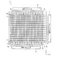
- FIG. 1 is a plan view for explaining a display element and an image display apparatus according to a first embodiment of the present invention.
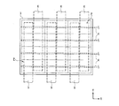
- FIG. 2 is an enlarged plan view showing a main configuration of the upper substrate side shown in FIG. 1 when viewed from the display surface side.
- FIG. 3 is an enlarged plan view showing the color filter layer on the lower substrate side shown in FIG. 1 when viewed from the non-display surface side.
- FIG. 4 is an enlarged plan view for explaining the electrode configuration on the lower substrate side shown in FIG. 1 when viewed from the non-display surface side.
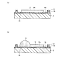
- FIG. 5A and FIG. 5B are cross-sectional views showing the main configuration of the display element shown in FIG. 1 during non-CF color display and CF color display, respectively.
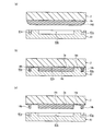
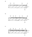
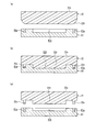
- FIG. 6 (a) to 6 (c) are diagrams for explaining the installation process of the structure shown in FIG. 5 (a).
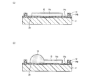
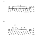
- FIG. 7A is a diagram for explaining the water repellent film forming step shown in FIG. 5A
- FIG. 7B is a diagram for explaining the polar liquid filling step shown in FIG. 5A. It is a figure to do.
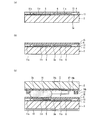
- FIG. 8A is a diagram for explaining the process of forming the color filter layer shown in FIG. 5A
- FIG. 8B is the formation of the reference electrode and the scan electrode shown in FIG.
- FIG. 8C is a diagram for explaining a process for forming the dielectric layer shown in FIG. 5A.
- FIG. 9A is a diagram for explaining a process for forming the signal electrode shown in FIG. 5A
- FIG. 9A is a diagram for explaining a process for forming the signal electrode shown in FIG. 5A
- FIG. 9A is a diagram for explaining a process for forming the signal electrode shown in FIG. 5A
- FIG. 9A
- FIG. 9B is a process for forming the water repellent film shown in FIG. 5A.
- FIG. 9C illustrates the final manufacturing process of the display element.
- FIG. 10 is a diagram for explaining an operation example of the image display device.
- FIG. 11A to FIG. 11C are diagrams for explaining the installation process of the structure in the display element according to the second embodiment of the present invention.
- FIGS. 12A and 12B are views for explaining a water repellent film forming step and a polar liquid filling step in the display element according to the second embodiment of the present invention, respectively.
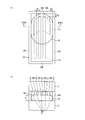
- FIG. 13 is an enlarged plan view showing a main configuration of the upper substrate side when viewed from the display surface side in the display element according to the third embodiment of the present invention.
- FIG. 14A is an enlarged plan view showing a main part configuration in one pixel region of the display element shown in FIG. 13, and FIG. 14B is a cross-sectional view taken along line XIVb-XIVb in FIG.
- FIG. 15A and FIG. 15B are cross-sectional views showing the main configuration of the display element shown in FIG. 13 during non-CF color display and CF color display, respectively.
- FIG. 16A to FIG. 16C are diagrams for explaining a process of installing the structure in the display element shown in FIG.
- FIGS. 17A and 17B are cross-sectional views showing the main configuration of the display element according to the fourth embodiment of the present invention during non-CF color display and CF color display, respectively.
- FIG. 18 (a) to 18 (d) are diagrams for explaining a structure installation process in the display element shown in FIG.
- FIG. 19 is an enlarged plan view showing a main configuration of the upper substrate side when viewed from the display surface side in the display element according to the fifth embodiment of the present invention.
- 20 (a) and 20 (b) are cross-sectional views showing the main configuration of the display element shown in FIG. 19 during non-CF color display and CF color display, respectively.
- FIG. 21A to FIG. 21C are diagrams for explaining a structure installation process in the display element shown in FIG.
- FIGS. 22A and 22B are views for explaining a water repellent film forming step and a polar liquid filling step in the display element shown in FIG. 19, respectively.
- FIG. 1 is a plan view for explaining a display element and an image display apparatus according to a first embodiment of the present invention.
- a display unit using the display element 10 of the present invention is provided, and a rectangular display surface is configured in the display unit. That is, the display element 10 includes an upper substrate 2 and a lower substrate 3 arranged so as to overlap each other in a direction perpendicular to the paper surface of FIG. An effective display area on the display surface is formed (details will be described later).
- a plurality of signal electrodes 4 are provided in stripes along the X direction at a predetermined interval from each other.
- a plurality of reference electrodes 5 and a plurality of scanning electrodes 6 are provided alternately in a stripe pattern along the Y direction.
- the plurality of signal electrodes 4, the plurality of reference electrodes 5, and the plurality of scan electrodes 6 are provided so as to intersect with each other.
- the signal electrodes 4 and the scan electrodes 6 are in units of intersections. A plurality of pixel areas are set.
- the plurality of signal electrodes 4, the plurality of reference electrodes 5, and the plurality of scan electrodes 6 are independently of each other a high voltage (hereinafter referred to as “H voltage”) as a first voltage and a second voltage.
- H voltage high voltage
- L voltage low voltage
- the plurality of pixel regions are partitioned by a partition wall, and the plurality of pixel regions correspond to a plurality of colors capable of full color display on the display surface side.
- a polar liquid described later is moved by an electrowetting phenomenon for each of a plurality of pixels (display cells) provided in a matrix, and the display color on the display surface side is changed. ing.
- the plurality of reference electrodes 5, and the plurality of scanning electrodes 6, one end side is drawn out to the outside of the effective display area of the display surface to form terminal portions 4a, 5a, and 6a. ing.
- a signal driver 7 is connected to each terminal portion 4a of the plurality of signal electrodes 4 via a wiring 7a.
- the signal driver 7 constitutes a signal voltage application unit.
- the signal driver 7 responds to the information for each of the plurality of signal electrodes 4.
- the signal voltage Vd is applied.
- a reference driver 8 is connected to each terminal portion 5a of the plurality of reference electrodes 5 via a wiring 8a.
- the reference driver 8 constitutes a reference voltage application unit.
- the reference driver 8 applies the reference voltage Vr to each of the plurality of reference electrodes 5. Is applied.
- a scanning driver 9 is connected to each terminal portion 6a of the plurality of scanning electrodes 6 via a wiring 9a.
- the scanning driver 9 constitutes a scanning voltage application unit.
- the scanning voltage Vs is applied to each of the plurality of scanning electrodes 6. Is applied.
- a non-selection voltage that prevents the polar liquid from moving with respect to each of the plurality of scan electrodes 6, and a selection voltage that allows the polar liquid to move according to the signal voltage Vd is applied as the scanning voltage Vs.
- the reference driver 8 is configured to operate with reference to the operation of the scanning driver 9, and the reference driver 8 prevents the polar liquid from moving with respect to each of the plurality of reference electrodes 5.
- One voltage of the non-selection voltage and the selection voltage that allows the polar liquid to move according to the signal voltage Vd is applied as the reference voltage Vr.
- the scanning driver 9 sequentially applies the selection voltage to the scanning electrodes 6 from the left side to the right side of FIG. 1, for example, and the reference driver 8 is synchronized with the operation of the scanning driver 9.
- the scanning operation is performed for each line by sequentially applying a selection voltage to the reference electrodes 5 from the left side to the right side of 1 (details will be described later).
- the signal driver 7, the reference driver 8, and the scanning driver 9 include a DC power supply or an AC power supply, and supply corresponding signal voltage Vd, reference voltage Vr, and scanning voltage Vs. .
- the reference driver 8 is configured to switch the polarity of the reference voltage Vr every predetermined time (for example, one frame).
- the scanning driver 9 is configured to switch each polarity of the scanning voltage Vs in response to switching of the polarity of the reference voltage Vr.
- FIG. 2 is an enlarged plan view showing a main configuration of the upper substrate side shown in FIG. 1 when viewed from the display surface side.
- FIG. 3 is an enlarged plan view showing the color filter layer on the lower substrate side shown in FIG. 1 when viewed from the non-display surface side.
- FIG. 4 is an enlarged plan view for explaining the electrode configuration on the lower substrate side shown in FIG. 1 when viewed from the non-display surface side.
- FIG. 5A and FIG. 5B are cross-sectional views showing the main configuration of the display element shown in FIG. 1 during non-CF color display and CF color display, respectively. 2 to 4, for simplification of the drawings, of the plurality of pixels provided on the display surface, twelve pixels arranged at the upper left end portion of FIG. 1 are illustrated. .
- the display element 10 includes the upper substrate 2 as a first substrate provided on the display surface side, and a second substrate provided on the back side (non-display surface side) of the upper substrate 2.
- the lower substrate 3 as a substrate is provided.
- the upper substrate 2 and the lower substrate 3 are arranged at a predetermined distance from each other, so that a predetermined display space S is formed between the upper substrate 2 and the lower substrate 3. .
- the polar liquid 16 and oil 17 as an insulating fluid that does not mix with the polar liquid 16 are contained in the display space S in the X direction (the left-right direction in FIG. 4).
- the polar liquid 16 can move to the effective display area P1 side or the non-effective display area P2 side described later.
- the polar liquid 16 for example, an aqueous solution containing water as a solvent and a predetermined electrolyte as a solute is used. Specifically, for example, an aqueous solution of 1 mmol / L potassium chloride (KCl) is used for the polar liquid 16.
- the polar liquid 16 is a predetermined color, for example, a color colored black with a self-dispersing pigment.
- the polar liquid 16 is colored black, the polar liquid 16 functions as a shutter that allows or blocks light transmission in each pixel. That is, in each pixel of the display element 10, as will be described in detail later, the polar liquid 16 moves inside the display space S on the reference electrode 5 side (effective display region P1 side) or on the scanning electrode 6 side (non-effective display region P2). The display color is changed to either black or RGB by sliding to the side).
- the oil 17 is a non-polar, colorless and transparent oil composed of one or more selected from, for example, side chain higher alcohol, side chain higher fatty acid, alkane hydrocarbon, silicone oil, and matching oil. It has been.
- the oil 17 moves in the display space S as the polar liquid 16 slides.
- a transparent glass material such as a non-alkali glass substrate or a transparent transparent sheet material such as a transparent synthetic resin such as an acrylic resin is used.
- the surface 2a on the non-display surface side (display space S side) of the upper substrate 2 includes the first and second rib members 14b and 14c as the partition walls so as to cover the entire surface.
- a body 14 is provided (details will be described later).
- a water repellent film 12 is formed on the surface of the structure 14.
- the lower substrate 3 is made of a transparent glass material such as a transparent glass material such as a non-alkali glass substrate or a transparent synthetic resin such as an acrylic resin, like the upper substrate 2.
- a color filter layer 11 is provided on the display surface side surface 3 a of the lower substrate 3.
- a reference electrode 5 and a scan electrode 6 are provided on the color filter layer 11, and a dielectric layer 13 is formed so as to cover the reference electrode 5 and the scan electrode 6.
- the signal electrode 4 is formed on the dielectric layer 13, and a water repellent film 15 is provided so as to cover the dielectric layer 13 and the signal electrode 4.
- a backlight 18 that emits white illumination light is integrally assembled on the back side (non-display surface side) of the lower substrate 3, and the transmissive display element 10 is configured.
- the backlight 18 uses a light source such as a cold cathode fluorescent tube or an LED.
- the color filter layer 11 includes red (R), green (G), and blue (B) color filter portions 11r, 11g, and 11b, and a black matrix portion 11s as a light shielding film.
- the pixels of each color of RGB are configured. That is, in the color filter layer 11, as illustrated in FIG. 3, RGB color filter portions 11r, 11g, and 11b are sequentially provided along the X direction, and each of the four color filter portions 11r, 11g, and 11b is Y. A total of 12 pixels are arranged in the X direction and the Y direction, respectively, 3 pixels and 4 pixels.
- any one of RGB color filter portions 11 r, 11 g, and 11 b is provided at a location corresponding to the effective display region P 1 of the pixel.
- a black matrix portion 11s is provided at a location corresponding to the ineffective display area P2. That is, in the display element 10, an ineffective display region P2 (non-opening portion) is set for the display space S by the black matrix portion (light-shielding film) 11s, and an opening portion (non-opening portion) formed in the black matrix portion 11s ( That is, the effective display area P1 is set by any one of the color filter portions 11r, 11g, and 11b).
- the area of the color filter portions 11r, 11g, and 11b is selected to be the same or slightly smaller than the area of the effective display area P1.
- the area of the black matrix portion 11s is selected to be the same or slightly larger than the area of the ineffective display area P2.
- FIG. 3 in order to clarify the boundary between adjacent pixels, the boundary between the two black matrix portions 11s corresponding to the adjacent pixels is indicated by a dotted line, but the actual color filter layer 11 Then, there is no boundary line between the black matrix portions 11s.
- the structure 14 has a covering surface 14a provided so as to cover the entire surface 2a of the upper substrate 2 on the display space S side, and is parallel to the Y direction and the X direction on the covering surface 14a.
- the rib partition wall which has the 1st rib member 14b and the 2nd rib member 14c which were provided in this way is contained.
- the structure 14 is provided on the surface 2a of the upper substrate 2 by a thermal imprint process using a mold.
- the display space S is divided in units of pixel regions P by the first and second rib members 14b and 14c. That is, in the display element 10, the display space S of each pixel is formed by two first rib members 14b facing each other and two second rib members 14c facing each other, as illustrated in FIG. It is partitioned. Further, in the display element 10, the polar liquid 16 is prevented from flowing into the display space S of the adjacent pixel region P by the first and second rib members 14b and 14c. That is, in the first and second rib members 14b and 14c, the protruding height (rib height) from the surface 2a of the upper substrate 2 is prevented so that the polar liquid 16 is prevented from flowing in and out between adjacent pixels. It has been decided.
- the water-repellent films 12 and 15 are made of a transparent synthetic resin, preferably, for example, a fluorine resin that becomes a hydrophilic layer with respect to the polar liquid 16 when a voltage is applied. Thereby, in the display element 10, the wettability (contact angle) between the polar liquid 16 on each surface side on the display space S side of the upper substrate 2 and the lower substrate 3 can be greatly changed. The moving speed of 16 can be increased.
- the dielectric layer 13 is made of a transparent dielectric film containing, for example, parylene, silicon nitride, hafnium oxide, zinc oxide, titanium dioxide, or aluminum oxide.
- each of the water repellent films 12 and 15 is several tens of nm to several ⁇ m, and the specific thickness dimension of the dielectric layer 13 is several hundred nm. Further, the water repellent film 15 does not electrically insulate the signal electrode 4 from the polar liquid 16 and does not hinder the improvement of the response of the polar liquid 16.
- a transparent electrode material such as indium oxide (ITO), tin oxide (SnO 2 ), or zinc oxide (AZO, GZO, or IZO) is used.
- ITO indium oxide
- SnO 2 tin oxide
- AZO zinc oxide
- GZO GZO
- IZO zinc oxide
- the signal electrode 4 uses a linear wiring arranged so as to be parallel to the X direction.
- the signal electrode 4 is made of a transparent electrode material such as ITO. Further, the signal electrode 4 is disposed on the dielectric layer 13 so as to pass through the central portion in the Y direction of each pixel region P, and is in electrical contact with the polar liquid 16 through the water repellent film 15. Is configured to do. Thereby, in the display element 10, the response of the polar liquid 16 during the display operation is improved.
- FIG. 6 (a) to 6 (c) are diagrams for explaining the installation process of the structure shown in FIG. 5 (a).
- FIG. 7A is a diagram for explaining the water repellent film forming step shown in FIG. 5A
- FIG. 7B is a diagram for explaining the polar liquid filling step shown in FIG. 5A. It is a figure to do.
- FIG. 8A is a diagram for explaining the process of forming the color filter layer shown in FIG. 5A
- FIG. 8B is the formation of the reference electrode and the scan electrode shown in FIG.
- FIG. 8C is a diagram for explaining a process for forming the dielectric layer shown in FIG. 5A.
- FIG. 9A is a diagram for explaining a process for forming the signal electrode shown in FIG. 5A
- FIG. 9B is a process for forming the water repellent film shown in FIG. 5A.
- FIG. 9C illustrates the final manufacturing process of the display element.
- a non-alkali glass substrate having a thickness of 0.7 mm, for example, is used as the upper substrate 2, and the structure 14 is formed on the upper substrate 2 so as to cover the entire surface 2a.
- An arrangement step of arranging the material layer 14X to be performed is performed.
- the material layer 14X includes, for example, methacrylic resin (PMMA), polyethylene (PE), polypropylene (PP), polystyrene (PS), acrylonitrile / styrene resin (AS), acrylonitrile / butadiene / styrene resin (ABS), or Thermoplastic general-purpose resins such as vinyl chloride (PVC) are used.
- a mold (mold) K1 is used in a subsequent installation step, and a metal material such as nickel is used for the mold K1.
- the mold K1 is provided with grooves K1a and K1b in advance for forming the first and second rib members 14b and 14c included in the structure 14.
- an installation step of providing the structure 14 on the surface 2a of the upper substrate 2 is performed. That is, in this installation step, a thermal imprint process (for example, temperature 140 ° C., pressure 10 MPa) using the mold K1 is performed, and the covering surface 14a, the first and second rib members 14b, 14c is formed on the surface 2a.
- a thermal imprint process for example, temperature 140 ° C., pressure 10 MPa
- the upper substrate 2 and the structure 14 are cooled, as shown in FIG. 6C, the upper substrate 2 and the structure 14 are released from the mold K1. And a predetermined primer process is performed with respect to the surface of the structure 14 before a subsequent formation process.
- a forming process for forming the water repellent film 12 on the surface of the structure 14 is performed. That is, in this forming step, the water repellent film 12 is formed by applying, for example, a fluorine-based resin material to the surface of the structure 14 by dipping and baking at 80 ° C. for 30 minutes.
- the film thickness of the water repellent film 12 is, for example, 60 nm.
- the adhesion between the surface of the structure 14 and the water-repellent film 12 is improved by performing the primer treatment.
- the upper substrate 2 is filled with a polar liquid 16. More specifically, in the upper substrate 2, the polar liquid 16 is filled into each pixel region P partitioned by the first and second rib members 14b and 14c by, for example, a dispenser device or an inkjet device.
- the oil 17 filling step is performed in the same manner before or after the polar liquid 16 filling step.
- a non-alkali glass substrate having a thickness of, for example, 0.7 mm is used for the lower substrate 3, and the color filter portions 11r, 11g, and 11b and the black are used by, for example, photolithography.
- the color filter layer 11 is formed by stacking the matrix portion 11s on the surface 3a of the lower substrate 3 to perform a CF forming step.
- the color filter layer 11 uses a photosensitive resin (for example, photoreactive acrylic monomer) and a corresponding pigment, and has a thickness of, for example, about 2 ⁇ m.
- an electrode forming process of the reference electrode 5 and the scanning electrode 6 is performed. That is, in this electrode formation step, the reference electrode 5 and the scan electrode 6 are formed by forming an ITO film having a thickness of 100 nm on the color filter layer 11 by, for example, sputtering.
- a dielectric layer 13 forming step is performed. That is, a silicon nitride film was formed as the dielectric layer 13 on the color filter layer 11, the reference electrode 5, and the scanning electrode 6 by using, for example, a CVD method.
- the film thickness of the dielectric layer 13 is, for example, 350 nm.
- an electrode forming process of the signal electrode 4 is performed. That is, the signal electrode 4 is installed on the surface of the dielectric layer 13 by fixing a thin wire made of, for example, ITO.
- a film forming process of the water repellent film 15 is performed. That is, a water-repellent film 15 was formed by applying, for example, a fluorine-based resin material to each surface of the dielectric layer 13 and the signal electrode 4 by dipping and baking at 80 ° C. for 30 minutes.
- the film thickness of the water repellent film 15 is, for example, 60 nm.
- the upper substrate 2 holding the polar liquid 16 and the oil 17 is integrated with the lower substrate 3 assembled from above using, for example, a UV adhesive, and then turned upside down. As a result, the display element 10 is completed.
- FIG. 10 is a diagram for explaining an operation example of the image display device.
- the reference driver 8 and the scanning driver 9 select the reference voltage Vr and the scanning voltage Vs as the reference voltage Vr and the scanning voltage Vs, respectively, for the reference electrode 5 and the scanning electrode 6 in a predetermined scanning direction from the left side to the right side in FIG. Apply voltage sequentially.
- the reference driver 8 and the scan driver 9 sequentially apply an H voltage (first voltage) and an L voltage (second voltage) as selection voltages to the reference electrode 5 and the scan electrode 6, respectively.
- the scanning operation for selecting the line is performed.
- the signal driver 7 applies the H voltage or the L voltage as the signal voltage Vd to the corresponding signal electrode 4 according to the image input signal from the outside.
- the polar liquid 16 is moved to the effective display area P1 side or the non-effective display area P2 side, and the display color on the display surface side is changed.
- the reference driver 8 and the scan driver 9 apply the non-selection voltage as the reference voltage Vr and the scan voltage Vs to the non-selected lines, that is, all the remaining reference electrodes 5 and scan electrodes 6, respectively.
- the reference driver 8 and the scan driver 9 apply an intermediate voltage (Middle) that is, for example, an intermediate voltage between the H voltage and the L voltage to the remaining reference electrodes 5 and scan electrodes 6 as non-selection voltages. Voltage, hereinafter referred to as “M voltage”).
- H voltage, L voltage, and M voltage are abbreviated as “H”, “L”, and “M”, respectively (the same applies to Table 2 described later).
- Specific values of the H voltage, the L voltage, and the M voltage are, for example, + 16V, 0V, and + 8V, respectively.
- ⁇ Operation on selected line> In the selection line, for example, when an H voltage is applied to the signal electrode 4, an H voltage is applied between the reference electrode 5 and the signal electrode 4. There is no potential difference with the electrode 4. On the other hand, since the L voltage is applied to the scan electrode 6 between the signal electrode 4 and the scan electrode 6, a potential difference is generated. Therefore, the polar liquid 16 moves in the display space S toward the scanning electrode 6 where a potential difference is generated with respect to the signal electrode 4. As a result, as illustrated in FIG. 5B, the polar liquid 16 is moved to the ineffective display area P ⁇ b> 2 side, and the oil 17 is moved to the reference electrode 5 side to illuminate light from the backlight 18. Is allowed to reach the color filter portion 11r.
- the display color on the display surface side is in a red display (CF color display) state by the color filter unit 11r.
- CF color display red display
- the polar liquid 16 moves to the ineffective display area P ⁇ b> 2 side and CF colored display is performed, from the RGB pixels.
- the red light, green light, and blue light are mixed with white light, and white display is performed.
- the polar liquid 16 moves in the display space S toward the reference electrode 5 where a potential difference is generated with respect to the signal electrode 4.
- the polar liquid 16 is moved to the effective display region P1 side, and the illumination light from the backlight 18 is prevented from reaching the color filter unit 11r.
- the display color on the display surface side is in a black display (non-CF color display) state by the polar liquid 16.
- the polar liquid 16 is maintained in a stationary state at the current position and is maintained in the current display color. That is, since the M voltage is applied to both the reference electrode 5 and the scan electrode 6, the potential difference between the reference electrode 5 and the signal electrode 4 and the potential difference between the scan electrode 6 and the signal electrode 4 are This is because the same potential difference occurs in both cases.
- the polar liquid 16 does not move but remains stationary and the display color on the display surface side. Does not change.
- the polar liquid 16 can be moved according to the voltage applied to the signal electrode 4 as described above, and the display color on the display surface side can be changed.
- the display color at each pixel on the selected line is applied to the signal electrode 4 corresponding to each pixel, for example, as shown in FIG. 10 by the combination of applied voltages shown in Table 1.
- the color filter portions 11r, 11g, and 11b are CF colored (red, green, or blue) or the non-CF colored (black) by the polar liquid 16.
- the reference driver 8 and the scanning driver 9 perform the scanning operation of the selection lines of the reference electrode 5 and the scanning electrode 6 from the left to the right in FIG. 10, for example, The display color also changes sequentially from left to right in FIG.
- the image display apparatus 1 can perform various information including moving images based on an external image input signal. Can be displayed.
- combinations of voltages applied to the reference electrode 5, the scan electrode 6, and the signal electrode 4 are not limited to Table 1 but may be those shown in Table 2.
- the reference driver 8 and the scan driver 9 are, for example, in a predetermined scanning direction from the left side to the right side in the figure, with respect to the reference electrode 5 and the scan electrode 6 as L voltage (second voltage) and H as selection voltages.
- a scanning operation is performed in which a voltage (first voltage) is sequentially applied to select lines.
- the signal driver 7 applies the H voltage or the L voltage as the signal voltage Vd to the corresponding signal electrode 4 according to the image input signal from the outside.
- the reference driver 8 and the scan driver 9 apply the M voltage as the non-selection voltage to the non-selected lines, that is, all the remaining reference electrodes 5 and scan electrodes 6.
- the polar liquid 16 moves in the display space S toward the reference electrode 5 where a potential difference is generated with respect to the signal electrode 4.
- the polar liquid 16 is moved to the effective display region P1 side, and the illumination light from the backlight 18 is prevented from reaching the color filter unit 11r.
- the display color on the display surface side is in a black display (non-CF color display) state by the polar liquid 16.
- the polar liquid 16 is maintained in a stationary state at the current position and is maintained at the current display color. That is, since the M voltage is applied to both the reference electrode 5 and the scan electrode 6, the potential difference between the reference electrode 5 and the signal electrode 4 and the potential difference between the scan electrode 6 and the signal electrode 4 are This is because the same potential difference occurs in both cases.
- the polar liquid 16 can be moved according to the voltage applied to the signal electrode 4 as described above, and the display color on the display surface side can be changed.
- the applied voltage to the signal electrode 4 is not limited to the binary value of the H voltage or the L voltage.
- the voltage between the H voltage and the L voltage can be changed according to information displayed on the display surface side.
- the image display device 1 can perform gradation display by controlling the signal voltage Vd. Thereby, the display element 10 excellent in display performance can be configured.
- the structure 14 covers the entire surface 2 a on the display space S side of the upper substrate 2.
- the adhesion of the water repellent film 12 can be easily increased, and occurrence of problems such as peeling of the water repellent film 12 can be prevented.
- the structure 14 of the present embodiment includes first and second rib members 14b and 14c provided so as to divide the inside of the display space S in accordance with each of the plurality of pixel regions P. ing.
- first and second rib members 14b and 14c provided so as to divide the inside of the display space S in accordance with each of the plurality of pixel regions P. ing.
- the structure 14 since the structure 14 is provided using the predetermined mold K1 in the installation step, the structure 14 can be provided with high accuracy.
- the image display device (electrical device) 1 even when the moving speed of the polar liquid 16 is increased, it is possible to prevent the occurrence of problems and the display element 10 having excellent reliability. Is used in the display unit, a high-performance image display device (electric device) 1 including a display unit with excellent reliability can be easily configured.
- the signal driver (signal voltage application unit) 7, the reference driver (reference voltage application unit) 8, and the scan driver (scan voltage application unit) 9 include the signal electrode 4, the reference electrode 5, The signal voltage Vd, the reference voltage Vr, and the scanning voltage Vs are applied to the scanning electrode 6. Accordingly, in the present embodiment, the matrix drive type display element 10 having excellent display quality can be easily configured, and the display color of each pixel region can be appropriately changed.
- FIG. 11A to FIG. 11C are diagrams for explaining the installation process of the structure in the display element according to the second embodiment of the present invention.
- FIGS. 12A and 12B are views for explaining a water repellent film forming step and a polar liquid filling step in the display element according to the second embodiment of the present invention, respectively.
- the main difference between the present embodiment and the first embodiment is that an ultraviolet curable synthetic resin material is used as the material layer of the structure, and the structure body is irradiated with ultraviolet rays in the installation process. This is the point.
- symbol is attached
- an ultraviolet curable synthetic resin material is used as the material layer 14X of the structure 14, and this material layer 14X is the entire surface 2a of the upper substrate 2. It is arranged to cover.
- each part (covered surface 14a, first and second rib members 14b, 14c) of the structure 14 is formed by performing a photolithography process using the mask members M1, M2. .
- FIG. 11B ultraviolet rays are irradiated from the material layer 14X side with the mask members M1 and M2 placed above the material layer 14X.
- FIG. 11C the material layer 14X is hatched diagonally to the left in FIG.
- a forming step of forming the water repellent film 12 on the surface of the structure 14 is performed. That is, in this forming step, the water repellent film 12 is formed by applying, for example, a fluorine-based resin material to the surface of the structure 14 by dipping and baking at 80 ° C. for 30 minutes.
- the film thickness of the water repellent film 12 is, for example, 60 nm.
- a filling process for filling the upper substrate 2 with the polar liquid 16 is performed. More specifically, in the upper substrate 2, the polar liquid 16 is filled into each pixel region P partitioned by the first and second rib members 14b and 14c by, for example, a dispenser device or an inkjet device.
- the oil 17 filling step is performed in the same manner before or after the polar liquid 16 filling step.
- the present embodiment can achieve the same operations and effects as the first embodiment. Moreover, in this embodiment, while using an ultraviolet curable synthetic resin material as the material layer 14X, the structure 14 is provided by irradiating with an ultraviolet-ray in an installation process. Thereby, the structure 14 can be provided easily.
- FIG. 13 is an enlarged plan view showing a main configuration of the upper substrate side when viewed from the display surface side in the display element according to the third embodiment of the present invention.
- FIG. 14A is an enlarged plan view showing a main part configuration in one pixel region of the display element shown in FIG. 13, and
- FIG. 14B is a cross-sectional view taken along line XIVb-XIVb in FIG.
- FIG. 15A and FIG. 15B are cross-sectional views showing the main configuration of the display element shown in FIG. 13 during non-CF color display and CF color display, respectively.
- the structure includes a rail member for forming a moving space for moving the insulating fluid, and the interface tension is low.
- a synthetic resin material having a high water repellency of 30 mN / m or less is used for the structure.
- symbol is attached
- the color filter layer 11, the signal electrode 4, the reference electrode 5, the scanning electrode 6, and the dielectric layer 13 are omitted for simplification of the drawing.
- the structure 24 is provided on the surface 2a of the upper substrate 2.
- the structure 24 includes a covering surface 24a provided so as to cover the entire surface 2a, and a first rib member 24b provided on the covering surface 24a so as to be parallel to the Y direction and the X direction, respectively.
- the frame-shaped rib (partition wall) which has the 2nd rib member 24c is provided.
- the first and second rib members 24b and 24c are configured to hermetically divide the pixel region P, unlike the first embodiment. That is, the first and second rib members 24b and 24c are connected to each other, and the end portion on the lower substrate 3 side is in contact with the lower substrate side.
- the structure 24 includes a plurality of, for example, four rail members 24d provided so as to protrude toward the lower substrate 3 in the frame-shaped rib. These four rail members 24d are provided at a predetermined interval from each other, and constitute a moving space for moving the oil (insulating fluid) 17. That is, as shown in FIGS. 14A and 14B, each rail member 24d protrudes from the upper substrate 2 side to the inner side of the display space S and on the upper substrate 2 side. It is provided in a straight line so as to connect the effective display area P1 and the non-effective display area P2, and the movement space K is partitioned inside the display space S.
- the movement space K for moving the oil (insulating fluid) 17 in each pixel region P is a display space. Inside S, the polar liquid 16 is formed on the upper substrate 2 side of the space in which it moves.
- the plurality of rail members 24d have one end side and the other end side inside the moving space K and the non-effective display region P1 side and the non-display side, respectively. It is provided on the effective display area P2 side and functions as a guide portion that guides the oil 17 to the effective display area P1 side or the non-effective display area P2 side in accordance with the movement of the polar liquid 16. Further, since each rail member 24d is not provided on the lower substrate 3 side on which the signal electrode 4, the reference electrode 5, the scanning electrode 6, and the dielectric layer 13 are installed, each rail member 24d has an electrowetting phenomenon. Is configured so as not to inhibit the movement of the polar liquid 16.
- the dimension h1 between the two adjacent rail members 24d, the first rib member 24b and the rail member 24d, , And the dimension h3 between the second rib member 24c and the rail member 24d is smaller than the dimension H of the polar liquid 16 in the direction perpendicular to the upper substrate 2 and the lower substrate 3, respectively.
- the dimensions h1 to h3 are each set to 10 ⁇ m, for example, and the dimension H is set to 40 ⁇ m, for example.
- the polar liquid 16 is mixed between the two adjacent rail members 24d, between the first rib member 24b and the rail member 24d, and the second rib member 24c. Can be prevented from entering between the rail member 24d and the rail member 24d. As a result, in this embodiment, it is possible to prevent the operation of the polar liquid 16 from becoming unstable.
- the polar liquid 16 is in the two adjacent rails.
- the operation of the polar liquid 16 was not stabilized by entering between the members 24d.
- the structure 24 is made of a highly water-repellent synthetic resin material having an interfacial tension of 30 mN / m or less, and the installation of the water-repellent film 12 is omitted.
- FIG. 16A to FIG. 16C are diagrams for explaining the installation process of the structure in the display element shown in FIG.
- an arrangement step of arranging the material layer 24X for forming the structure 24 is performed so as to cover the entire surface 2a of the upper substrate 2.
- a synthetic resin material having high water repellency having an interfacial tension of 30 mN / m or less such as polypropylene (PP), polymethylpentene (TPX), or polytetrafluoroethylene (PTFE), is used. Yes.
- the material layer 24X has a low interfacial tension as described above, the material layer 24X is poured into the mold K3 in advance in the arrangement step of the present embodiment.
- the mold K3 is provided with grooves K3a, K3b, and K3c for forming the first and second rib members 24b, 24c and the rail member 24d included in the structure 24 in advance. .
- the upper substrate is subsequently continued.
- the installation process which provides the structure 24 on the surface 2a of 2 is performed. That is, in the arranging step, the material layer 24X is arranged on the surface 2a by superimposing the surface 2a of the upper substrate 2 from above the mold K3 into which the material layer 24X has been poured. Thereafter, in the installation process, a thermal imprint process (for example, a temperature of 140 ° C. and a pressure of 10 MPa) using the mold K3 is performed, and the covering surface 24a, the first and second rib members 24b, 24c are performed. , And a rail member 24d is formed on the surface 2a.
- a thermal imprint process for example, a temperature of 140 ° C. and a pressure of 10 MPa
- the present embodiment can achieve the same operations and effects as the first embodiment. Further, in the present embodiment, a synthetic resin material having a high water repellency having an interfacial tension of 30 mN / m or less is used as the structure 24. Therefore, unlike the first embodiment, the water repellent film 12 The moving speed of the polar liquid 16 can be easily improved by the structure 24 while omitting the installation.
- the structure 24 of the present embodiment includes a rail member 24d that is provided for each pixel region P and that constitutes a movement space K for moving the oil 17.
- FIGS. 17A and 17B are cross-sectional views showing the main configuration of the display element according to the fourth embodiment of the present invention during non-CF color display and CF color display, respectively.
- the main difference between this embodiment and the third embodiment is that a synthetic resin material to which a modifier is added is used for the structure.
- symbol is attached
- the structure 34 is provided on the surface 2a of the upper substrate 2.
- the structure 34 has a covering surface 34a provided so as to cover the entire surface 2a, and a first rib member 34b provided on the covering surface 34a so as to be parallel to the Y direction and the X direction, respectively.
- the frame-shaped rib (partition wall) which has the 2nd rib member 34c is provided.
- the first and second rib members 34b and 34c are configured to hermetically divide the pixel region P in the same manner as in the third embodiment. That is, the first and second rib members 34b and 34c are connected to each other, and the end portion on the lower substrate 3 side is in contact with the lower substrate side.
- the structure 34 includes a plurality of, for example, four rail members 34d provided so as to protrude toward the lower substrate 3 in the frame-shaped rib, as in the third embodiment. ing.
- These four rail members 34d are provided at a predetermined interval from each other, and constitute a movement space for moving the oil (insulating fluid) 17. That is, as shown in FIGS. 17A and 17B, each rail member 34d protrudes from the upper substrate 2 side to the inner side of the display space S and on the upper substrate 2 side. It is provided in a straight line so as to connect the effective display area P1 and the non-effective display area P2, and the movement space is partitioned inside the display space S.
- the movement space for moving the oil (insulating fluid) 17 in each pixel region P is the display space S, as in the third embodiment. Is formed on the upper substrate 2 side of the space in which the polar liquid 16 moves.
- the structure 34 is made into a highly water-repellent material having an interfacial tension of 30 mN / m or less. It has been modified.
- 18 (a) to 18 (d) are diagrams for explaining the installation process of the structure in the display element shown in FIG.
- a reforming process for modifying the material layer 34X is performed. That is, in this modification step, by adding a modifier to the synthetic resin material as the material layer 34X, the synthetic resin material is modified into a highly water-repellent material having an interfacial tension of 30 mN / m or less. Quality is done. Specifically, the material layer 34X is poured into the mold K4 in advance, and by adding a modifier to the material layer 34X, the material layer 34X is changed to the above highly water-repellent material. It has been.
- the material layer 34X is modified to a highly water-repellent material having an interfacial tension of 30 mN / m or less. Has been.
- the mold K4 is provided with grooves K4a, K4b, and K4c for forming the first and second rib members 34b, 34c and the rail member 34d included in the structure 34 in advance.
- the upper substrate 2 is disposed above the modified material layer 34X with the surface 2a facing down.
- the upper substrate is subsequently continued.
- the installation process which provides the structure 34 on the surface 2a of 2 is performed. That is, in the arranging step, the material layer 34X is arranged on the surface 2a by overlapping the surface 2a of the upper substrate 2 from above the mold K4 into which the material layer 34X has been poured. Thereafter, in the installation process, a thermal imprint process (for example, a temperature of 140 ° C. and a pressure of 10 MPa) using the mold K4 is performed, and the covering surface 34a, the first and second rib members 34b, 34c are performed. , And a rail member 34d is formed on the surface 2a.
- a thermal imprint process for example, a temperature of 140 ° C. and a pressure of 10 MPa
- the present embodiment can achieve the same operations and effects as the third embodiment.
- a synthetic resin material that is modified to a highly water-repellent material having an interfacial tension of 30 mN / m or less by adding a modifier is used as the structure 34.
- options such as the kind of synthetic resin material that can constitute the structure 34 that can easily improve the moving speed of the polar liquid 16 while omitting the installation of the water repellent film 12 by the modifier.
- the degree of freedom in designing the structure 34 can also be increased.
- FIG. 19 is an enlarged plan view showing a main configuration of the upper substrate side when viewed from the display surface side in the display element according to the fifth embodiment of the present invention.
- 20 (a) and 20 (b) are cross-sectional views showing the main configuration of the display element shown in FIG. 19 during non-CF color display and CF color display, respectively.
- the main difference between this embodiment and the first embodiment is that the upper substrate and the structure are provided integrally.
- symbol is attached
- the upper substrate 22 includes a substrate body 22a that functions as an upper substrate (first substrate) and a structure 22b that is provided integrally with the substrate body 22a.
- the structure 22b includes a first rib member 22c and a second rib member 22d as in the first embodiment.
- FIGS. 22A and 22B are views for explaining a water repellent film forming step and a polar liquid filling step in the display element shown in FIG. 19, respectively.
- a material layer 22X is provided on the substrate body 22a, and the material layer 22X is disposed above the mold K1.
- an installation step of providing the structure 22b on the surface side of the upper substrate 22 is performed. That is, in this installation process, a thermal imprint process (for example, a temperature of 140 ° C. and a pressure of 10 MPa) using the mold K1 is performed, and the first and second rib members 22c and 22d are on the surface side. Formed.
- a thermal imprint process for example, a temperature of 140 ° C. and a pressure of 10 MPa
- the upper substrate 22 is released from the mold K1 as shown in FIG. 21 (c). And a predetermined primer process is performed with respect to the surface of the structure 22b before a subsequent formation process.
- the surface of the structure 22b that is, the surfaces of the first and second rib members 22c and 22d, and the first and second rib members 22c and 22d of the substrate body 22a.
- a forming step of forming the water-repellent film 12 on the surface of the portion where no is formed is performed. That is, in this forming step, the water repellent film 12 is formed by applying, for example, a fluorine-based resin material to the surface of the structure 22b by dipping and baking at 80 ° C. for 30 minutes.
- the film thickness of the water repellent film 12 is, for example, 60 nm.
- the adhesion between the surface of the structure 22b and the water repellent film 12 is improved.
- a filling step for filling the upper substrate 22 with the polar liquid 16 is performed.
- the polar liquid 16 is filled into each pixel region P partitioned by the first and second rib members 22c and 22d, for example, by a dispenser device or an ink jet device.
- the oil 17 filling step is performed in the same manner before or after the polar liquid 16 filling step.
- the present embodiment can achieve the same operations and effects as the first embodiment.
- the upper substrate 22 and the structure 22b are integrally provided, it is possible to easily obtain the display element 10 with a small number of components and easy to manufacture.
- the upper substrate and the structure may be integrally formed using a transparent glass material such as an alkali-free glass substrate.
- the upper substrate and the structure are integrally formed using the ultraviolet curable resin material shown in the second embodiment, or the highly water-repellent synthetic resin shown in the third or fourth embodiment.
- a structure in which the upper substrate and the structure are integrally formed using a material may be used.
- the present invention is an electric device provided with a display unit that displays information including characters and images.
- the present invention is not limited in any way.
- a portable information terminal such as a PDA such as an electronic notebook, a display device attached to a personal computer, a television, or the like, or an electronic paper or other electric device including various display units. it can.
- the display element of the present invention is not limited to this. It is not limited as long as it is an electric field induction type display element that can change the display color on the display surface side by operating a polar liquid inside the display space using an external electric field. Instead, the present invention can be applied to other types of electric field induction display elements such as an electroosmosis method, an electrophoresis method, and a dielectrophoresis method.
- the electrowetting type display element when configured as in the above embodiments, the polar liquid can be moved at a high speed with a low driving voltage. Further, in the electrowetting type display element, the display color is changed according to the movement of the polar liquid, and unlike a liquid crystal display device using a birefringent material such as a liquid crystal layer, it is used for information display. It is also preferable in that a high-luminance display element that is excellent in light utilization efficiency of light from the backlight and external light can be easily configured. Furthermore, since it is not necessary to provide a switching element for each pixel, it is also preferable in that a high-performance matrix driving display element having a simple structure can be configured at low cost.
- the present invention provides a structure for driving a polar liquid for each pixel region so as to cover the entire surface of the display space side of the substrate on at least one side of the first and second substrates. There is no limitation as long as it is provided.
- a plurality of signal electrodes and a plurality of scanning electrodes are provided in a matrix so as to cross each other, and for each of a plurality of pixel regions provided in units of intersections between the signal electrodes and the scanning electrodes, A switching element such as a thin film transistor (TFT) is installed.
- TFT thin film transistor
- the scanning electrode is connected to the gate of the thin film transistor, and the voltage is applied from the scanning voltage application unit.
- the signal electrode is connected to the source of the thin film transistor and voltage is applied from the signal voltage application unit, and the drain of the thin film transistor is connected to the pixel electrode provided for each pixel region to supply the voltage from the signal electrode.
- the polar liquid may be moved.
- the reference electrode and the reference driver reference voltage application unit
- a transmissive display element including a backlight is configured.
- the present invention is not limited to this, and a reflective type having a light reflecting portion such as a diffuse reflector.
- the present invention can also be applied to a transflective display element in which the light reflecting portion and the backlight are used in combination.
- the structure of the present invention may be used for driving polar liquid for each pixel region. It is not limited at all.
- the structure of the present invention is provided on at least one side of the first and second substrates.
- the structure may be provided so as to cover the entire surface on the display space side, and the structure is provided on the lower substrate (second substrate), or a part of the structure and the remaining part of the structure are provided respectively.
- substrate may be sufficient.
- polar liquids include zinc chloride, potassium hydroxide, sodium hydroxide, alkali metal hydroxide, zinc oxide, sodium chloride, lithium salt, phosphoric acid, alkali metal carbonate, oxygen ion conductivity.
- polar liquids include zinc chloride, potassium hydroxide, sodium hydroxide, alkali metal hydroxide, zinc oxide, sodium chloride, lithium salt, phosphoric acid, alkali metal carbonate, oxygen ion conductivity.
- Those containing an electrolyte such as ceramics can be used.
- organic solvents such as alcohol, acetone, formamide, and ethylene glycol can also be used as the solvent.
- the polar liquid of the present invention includes an ionic liquid containing a cation such as pyridine, alicyclic amine, or aliphatic amine, and an anion such as fluoride such as fluoride ion or triflate ( Room temperature molten salt) can also be used.
- a cation such as pyridine, alicyclic amine, or aliphatic amine
- an anion such as fluoride such as fluoride ion or triflate ( Room temperature molten salt) can also be used.
- the polar liquid of the present invention includes a conductive liquid having conductivity and a liquid having a high dielectric constant having a specific dielectric constant of a predetermined value or higher, preferably 15 or higher.
- the use of an aqueous solution in which a predetermined electrolyte is dissolved in a polar liquid is superior in handleability and can easily constitute a display element that is easy to manufacture. Is preferable.
- the insulating fluid of the present invention includes a fluid having a relative dielectric constant of not more than a predetermined value, preferably not more than 5.
- the use of nonpolar oil that is not compatible with polar liquid is more polar in the nonpolar oil than when air and polar liquid are used. It is preferable in that the liquid droplets can be moved more easily, the polar liquid can be moved at high speed, and the display color can be switched at high speed.
- the signal electrode is installed inside the display space so as to be in contact with the polar liquid
- the reference electrode and the scan electrode are connected to the first and second electrodes while being electrically insulated from the polar liquid.
- the signal electrode may be provided in the middle portion of the first and second substrates
- the reference electrode and the scan electrode may be provided on the first substrate side.
- the present invention is not limited to this, and the reference electrode and the scan electrode May be installed on the non-effective display area side and the effective display area side, respectively.
- the present invention is not limited to this, and the insulating material It is also possible to use a reference electrode and a scan electrode embedded in the second substrate.
- the second substrate can be used as a dielectric layer, and the installation of the dielectric layer can be omitted.
- the signal electrode may be directly provided on the first and second substrates also serving as the dielectric layer, and the signal electrode may be installed inside the display space.
- the present invention is installed so as to face the effective display area of the pixel among the reference electrode and the scan electrode. It is sufficient that only one of the electrodes is made of a transparent electrode material, and an opaque electrode material such as aluminum, silver, chromium, or other metal can be used for the other electrode that is not opposed to the effective display area. .
- the shapes of the reference electrode and the scan electrode of the present invention are not limited to this.
- the shape may be such that light loss such as a line shape or a net shape hardly occurs.
- the signal electrode of the present invention is not limited to this, and wiring formed in other shapes such as a mesh wiring may also be used. Can be used.
- the present invention is not limited to this.
- the plurality of pixel regions are provided in accordance with a plurality of colors capable of full color display on the display surface side.
- a plurality of polar liquids colored in RGB, cyan (C), magenta (M), yellow (Y), CMY, or RGBYC can be used.
- the color filter layer is formed on the surface of the lower substrate (second substrate) on the display surface side.
- the present invention is not limited to this, and the second substrate.
- a color filter layer can also be provided on the surface on the non-display surface side or on the upper substrate (first substrate) side.
- the case where the color filter layer is used is preferable in that a display element which is easy to manufacture can be easily configured as compared with the case where a plurality of colors of polar liquids are prepared.
- the color filter part (opening part) and the black matrix part (light-shielding film) included in the color filter layer appropriately and reliably provide an effective display area and an ineffective display area with respect to the display space. It is also preferable in that it can be set.
- the present invention can prevent the occurrence of problems even when the moving speed of a polar liquid is increased, and has a display device having excellent reliability, a manufacturing method thereof, and an electric device using the display device Useful for.
Landscapes
- Physics & Mathematics (AREA)
- General Physics & Mathematics (AREA)
- Optics & Photonics (AREA)
- Electrochromic Elements, Electrophoresis, Or Variable Reflection Or Absorption Elements (AREA)
Abstract
上部基板(第1の基板)(2)と、下部基板(第2の基板)(3)と、上部基板(2)及び下部基板(3)の間に形成された表示用空間(S)の内部で有効表示領域(P1)側または非有効表示領域(P2)側に移動可能に封入された極性液体(16)とを具備した表示素子(10)において、上部基板(2)の表示用空間(S)側の表面(2a)の全面を覆うように、画素領域(P)毎に、極性液体(16)を駆動するためのリブ(構造体)(14a~14c)を設ける。
Description
本発明は、極性液体を移動させることにより、画像や文字などの情報を表示する表示素子、その製造方法、及びその表示素子を用いた電気機器に関する。
近年、表示素子では、エレクトロウェッティング方式の表示素子に代表されるように、外部電界による極性液体の移動現象を利用して、情報の表示を行うものが開発され、実用化されている。
具体的にいえば、上記のような従来の表示素子では、例えば下記特許文献1に記載されているように、第1及び第2の基板の間に表示用空間を形成するとともに、リブ(仕切壁)によって当該表示用空間の内部を複数の各画素領域に応じて区切っていた。また、この従来の表示素子では、上記の各画素領域において、導電性液体(極性液体)が封入されるとともに、信号電極と、互いに平行に設けられた走査電極及び基準電極(参照電極)とが交差するように設けられていた。そして、この従来の表示素子では、各画素領域において、信号電極、走査電極、及び基準電極に対し電圧印加を適宜行うことにより、導電性液体を走査電極側または基準電極側に移動させて、表示面側の表示色を変更するようになっていた。
しかしながら、上記のような従来の表示素子では、導電性液体(極性液体)の移動速度の高速化を図ったときに、不具合が表示素子に発生し、その信頼性が低下するという問題点を生じるおそれがあった。
具体的にいえば、上記従来の表示素子では、導電性液体の移動速度の高速化を図るために、走査電極及び基準電極(参照電極)が設けられた第1及び第2の基板の一方の表示用空間側の表面に誘電体層を設けたり、この誘電体層の表面及び第1及び第2の基板の他方の表示用空間側の表面に撥水膜を設けたりしていた。ところが、従来の表示素子では、誘電体層の表面上や第1及び第2の基板の他方の表示用空間側の表面上に上記リブ(構造体)を形成した後、撥水膜を設けていた。このため、リブと誘電体層、第1、または第2の基板とに対する撥水膜の密着性が異なるものとなって、当該撥水膜の剥離等の不具合を生じることがあった。この結果、従来の表示素子では、その信頼性が低下するという問題点を生じるおそれがあった。
上記の課題を鑑み、本発明は、極性液体の移動速度の高速化を図ったときでも、不具合が生じるのを防ぐことができ、優れた信頼性を有する表示素子、その製造方法、及びその表示素子を用いた電気機器を提供することを目的とする。
上記の目的を達成するために、本発明にかかる表示素子は、表示面側に設けられた第1の基板と、所定の表示用空間が前記第1の基板との間に形成されるように、当該第1の基板の非表示面側に設けられた第2の基板と、前記表示用空間に対し、設定された有効表示領域及び非有効表示領域と、前記表示用空間の内部で前記有効表示領域側または前記非有効表示領域側に移動可能に封入された極性液体とを具備し、前記極性液体を移動させることにより、前記表示面側の表示色を変更可能に構成された表示素子であって、
前記極性液体と接触するように、前記表示用空間の内部に設置されるとともに、所定の配列方向に沿って設けられた複数の信号電極、
前記有効表示領域側及び前記非有効表示領域側の一方側に設置されるように、前記極性液体に対して電気的に絶縁された状態で、前記第1及び第2の基板の一方側に設けられるとともに、前記複数の信号電極と交差するように設けられた複数の走査電極、
前記信号電極と前記走査電極との交差部単位に設けられた複数の画素領域、
及び
前記表示用空間の内部に前記画素領域毎に移動可能に封入されるとともに、前記極性液体と混じり合わない絶縁性流体を備え、
前記第1及び第2の基板の少なくとも一方側において、その基板の前記表示用空間側の表面の全面を覆うように、前記画素領域毎に、前記極性液体を駆動するための構造体を設けたことを特徴とするものである。
前記極性液体と接触するように、前記表示用空間の内部に設置されるとともに、所定の配列方向に沿って設けられた複数の信号電極、
前記有効表示領域側及び前記非有効表示領域側の一方側に設置されるように、前記極性液体に対して電気的に絶縁された状態で、前記第1及び第2の基板の一方側に設けられるとともに、前記複数の信号電極と交差するように設けられた複数の走査電極、
前記信号電極と前記走査電極との交差部単位に設けられた複数の画素領域、
及び
前記表示用空間の内部に前記画素領域毎に移動可能に封入されるとともに、前記極性液体と混じり合わない絶縁性流体を備え、
前記第1及び第2の基板の少なくとも一方側において、その基板の前記表示用空間側の表面の全面を覆うように、前記画素領域毎に、前記極性液体を駆動するための構造体を設けたことを特徴とするものである。
上記のように構成された表示素子では、第1及び第2の基板の少なくとも一方側において、上記構造体がその基板の表示用空間側の表面の全面を覆うように、設けられている。これにより、上記従来例と異なり、極性液体の移動速度の高速化を図ったときでも、不具合が生じるのを防ぐことができ、優れた信頼性を有する表示素子を構成することができる。
また、上記表示素子において、前記構造体の表面上には、撥水膜が形成されてもよい。
この場合、撥水膜が構造体の上記表示用空間側の表面を覆うように形成されることとなり、極性液体の移動速度を容易に向上させることができる。
また、上記表示素子において、前記構造体として、界面張力が30mN/m以下である撥水性の高い合成樹脂材料が用いられてもよい。
この場合、撥水膜の設置を割愛しつつ、極性液体の移動速度を容易に向上させることができる。
また、上記表示素子において、前記構造体として、改質剤が添加されることにより、界面張力が30mN/m以下である撥水性の高い材料に改質された合成樹脂材料が用いられていることが好ましい。
この場合、改質剤によって、撥水膜の設置を割愛しつつ、極性液体の移動速度を容易に向上可能な構造体を構成できる合成樹脂材料の種類などの選択肢を広げることができ、当該構造体の設計自由度も広げることができる。
また、上記表示素子において、前記第1及び第2の基板の少なくとも一方と前記構造体とが、一体的に設けられてもよい。
この場合、部品点数が少なく製造簡単な表示素子を容易に得ることができる。
また、上記表示素子において、前記構造体には、前記複数の各画素領域に応じて、前記表示用空間の内部を区切るように、設けられたリブ部材が含まれてもよい。
この場合、隣接する画素領域内に極性液体が流入するのを容易に防ぐことができ、優れた表示品位を有する表示素子を容易に構成することができる。
また、上記表示素子において、前記構造体には、前記画素領域毎に設けられるとともに、前記絶縁性流体を移動させるための移動用空間を構成するためのレール部材が含まれてもよい。
この場合、極性液体の移動速度の高速化をより容易に図ることができる。
また、上記表示素子において、前記複数の信号電極に接続されるとともに、前記複数の各信号電極に対して、前記表示面側に表示される情報に応じて、所定の電圧範囲内の信号電圧を印加する信号電圧印加部と、
前記複数の走査電極に接続されるとともに、前記複数の各走査電極に対して、前記極性液体が前記信号電圧に応じて、前記表示用空間の内部を移動するのを許容する選択電圧と、前記極性液体が前記表示用空間の内部を移動するのを阻止する非選択電圧との一方の電圧を印加する走査電圧印加部とを備えていることが好ましい。
前記複数の走査電極に接続されるとともに、前記複数の各走査電極に対して、前記極性液体が前記信号電圧に応じて、前記表示用空間の内部を移動するのを許容する選択電圧と、前記極性液体が前記表示用空間の内部を移動するのを阻止する非選択電圧との一方の電圧を印加する走査電圧印加部とを備えていることが好ましい。
この場合、各画素領域の表示色を適切に変更することができる。
また、上記表示素子において、前記複数の画素領域が、前記表示面側でフルカラー表示が可能な複数の色に応じてそれぞれ設けられてもよい。
この場合、複数の各画素において対応する極性液体が適切に移動されることにより、カラー画像表示を行うことができる。
また、上記表示素子において、前記有効表示領域側及び前記非有効表示領域側の他方側に設置されるように、前記極性液体及び前記走査電極に対して電気的に絶縁された状態で、前記第1及び第2の基板の一方側に設けられるとともに、前記複数の信号電極と交差するように設けられた複数の参照電極と、
前記複数の参照電極に接続されるとともに、前記複数の各参照電極に対して、前記極性液体が前記信号電圧に応じて、前記表示用空間の内部を移動するのを許容する選択電圧と、前記極性液体が前記表示用空間の内部を移動するのを阻止する非選択電圧との一方の電圧を印加する参照電圧印加部とが設けられていることが好ましい。
前記複数の参照電極に接続されるとともに、前記複数の各参照電極に対して、前記極性液体が前記信号電圧に応じて、前記表示用空間の内部を移動するのを許容する選択電圧と、前記極性液体が前記表示用空間の内部を移動するのを阻止する非選択電圧との一方の電圧を印加する参照電圧印加部とが設けられていることが好ましい。
この場合、スイッチング素子を画素領域毎に設けることなく、表示不良が生じるのを防ぐことができるマトリクス駆動方式の表示素子を構成することができる。
また、上記表示素子において、前記参照電極及び前記走査電極の表面上には、誘電体層が積層されていることが好ましい。
この場合、誘電体層が極性液体に印加する電界を確実に大きくして、当該極性液体の移動速度をより容易に向上することができる。
また、上記表示素子において、前記非有効表示領域は、前記第1及び第2の基板の一方側に設けられた遮光膜によって設定され、
前記有効表示領域は、前記遮光膜に形成された開口部によって設定されていることが好ましい。
前記有効表示領域は、前記遮光膜に形成された開口部によって設定されていることが好ましい。
この場合、表示用空間に対し、有効表示領域及び非有効表示領域を適切に、かつ、確実に設定することができる。
また、本発明の電気機器は、文字及び画像を含んだ情報を表示する表示部を備えた電気機器であって、
前記表示部に、上記いずれかの表示素子を用いたことを特徴とするものである。
前記表示部に、上記いずれかの表示素子を用いたことを特徴とするものである。
上記のように構成された電気機器では、極性液体の移動速度の高速化を図ったときでも、不具合が生じるのを防ぐことができ、優れた信頼性を有する表示素子が表示部に用いられているので、信頼性に優れた表示部を備えた高性能な電気機器を容易に構成することができる。
また、本発明の表示素子の製造方法は、表示面側に設けられた第1の基板と、所定の表示用空間が前記第1の基板との間に形成されるように、当該第1の基板の非表示面側に設けられた第2の基板と、前記表示用空間に対し、複数の画素領域毎に設定された有効表示領域及び非有効表示領域と、前記表示用空間の内部で前記有効表示領域側または前記非有効表示領域側に移動可能に封入された極性液体及び前記極性液体と混じり合わない絶縁性流体を具備し、前記極性液体を移動させることにより、前記表示面側の表示色を変更可能に構成された表示素子の製造方法であって、
前記第1及び第2の基板の少なくとも一方側において、その基板の前記表示用空間側の表面の全面を覆うように、前記画素領域毎に、前記極性液体を駆動するための構造体を形成する材料層を配置する配置工程と、
前記材料層に対して、所定の処理を施すことにより、前記第1及び第2の基板の少なくとも一方側の前記表面上に前記構造体を設ける設置工程とを備えていることを特徴とするものである。
前記第1及び第2の基板の少なくとも一方側において、その基板の前記表示用空間側の表面の全面を覆うように、前記画素領域毎に、前記極性液体を駆動するための構造体を形成する材料層を配置する配置工程と、
前記材料層に対して、所定の処理を施すことにより、前記第1及び第2の基板の少なくとも一方側の前記表面上に前記構造体を設ける設置工程とを備えていることを特徴とするものである。
上記のように構成された表示素子の製造方法では、上記配置工程及び設置工程を順次行うことにより、第1及び第2の基板の少なくとも一方側において、その基板の表示用空間側の表面の全面を覆うように、上記構造体を設けることができる。これにより、上記従来例と異なり、極性液体の移動速度の高速化を図ったときでも、不具合が生じるのを防ぐことができ、優れた信頼性を有する表示素子を構成することができる。
また、上記表示素子の製造方法において、前記設置工程では、所定の金型を用いて、前記構造体が設けられてもよい。
この場合、構造体を精度よく設けることができる。
また、上記表示素子の製造方法において、前記材料層として、紫外線硬化合成樹脂材料を用いるとともに、
前記設置工程では、紫外線を照射することにより、前記構造体が設けられてもよい。
前記設置工程では、紫外線を照射することにより、前記構造体が設けられてもよい。
この場合、構造体を容易に設けることができる。
また、上記表示素子の製造方法において、前記設置工程の後に、前記構造体の表面上に、撥水膜を形成する形成工程を行ってもよい。
この場合、撥水膜が構造体の上記表示用空間側の表面を覆うように形成されることとなり、極性液体の移動速度を容易に向上させることができる。
また、上記表示素子の製造方法において、前記配置工程において、前記材料層として、界面張力が30mN/m以下である撥水性の高い合成樹脂材料を用いるとともに、前記第1及び第2の基板の少なくとも一方側または所定の金型に当該合成樹脂材料を配置してもよい。
この場合、撥水膜の設置を割愛しつつ、極性液体の移動速度を容易に向上させることができる。
また、上記表示素子の製造方法において、前記配置工程の前に、前記材料層としての合成樹脂材料に対し、改質剤を添加することにより、当該合成樹脂材料を、界面張力が30mN/m以下である撥水性の高い材料に改質する改質工程を行ってもよい。
この場合、改質剤によって、撥水膜の設置を割愛しつつ、極性液体の移動速度を容易に向上可能な構造体を構成できる合成樹脂材料の種類などの選択肢を広げることができ、当該構造体の設計自由度も広げることができる。
本発明によれば、極性液体の移動速度の高速化を図ったときでも、不具合が生じるのを防ぐことができ、優れた信頼性を有する表示素子、その製造方法、及びその表示素子を用いた電気機器を提供することが可能となる。
以下、本発明の表示素子及び電気機器の好ましい実施形態について、図面を参照しながら説明する。尚、以下の説明では、カラー画像表示を表示可能な表示部を備えた画像表示装置に本発明を適用した場合を例示して説明する。また、各図中の構成部材の寸法は、実際の構成部材の寸法及び各構成部材の寸法比率等を忠実に表したものではない。
[第1の実施形態]
図1は、本発明の第1の実施形態にかかる表示素子、及び画像表示装置を説明する平面図である。図1において、本実施形態の画像表示装置1では、本発明の表示素子10を用いた表示部が設けられており、この表示部には矩形状の表示面が構成されている。すなわち、表示素子10は、図1の紙面に垂直な方向で互いに重ね合うように配置された上部基板2及び下部基板3を備えており、これらの上部基板2と下部基板3との重なり部分によって上記表示面の有効表示領域が形成されている(詳細は後述。)。
図1は、本発明の第1の実施形態にかかる表示素子、及び画像表示装置を説明する平面図である。図1において、本実施形態の画像表示装置1では、本発明の表示素子10を用いた表示部が設けられており、この表示部には矩形状の表示面が構成されている。すなわち、表示素子10は、図1の紙面に垂直な方向で互いに重ね合うように配置された上部基板2及び下部基板3を備えており、これらの上部基板2と下部基板3との重なり部分によって上記表示面の有効表示領域が形成されている(詳細は後述。)。
また、表示素子10では、複数の信号電極4が互いに所定の間隔をおいて、かつ、X方向に沿ってストライプ状に設けられている。また、表示素子10では、複数の参照電極5及び複数の走査電極6が、互いに交互に、かつ、Y方向に沿ってストライプ状に設けられている。これら複数の信号電極4と、複数の参照電極5及び複数の走査電極6とは、互いに交差するように設けられており、表示素子10では、信号電極4と走査電極6との交差部単位に、複数の各画素領域が設定されている。
また、これら複数の信号電極4、複数の参照電極5、及び複数の走査電極6は、互いに独立して、第1の電圧としてのHigh電圧(以下、“H電圧”という。)と、第2の電圧としてのLow電圧(以下、“L電圧”という。)との間の所定の電圧範囲内の電圧が印加可能に構成されている(詳細は後述。)。
さらに、表示素子10では、後に詳述するように、上記複数の各画素領域が仕切壁にて区切られるとともに、複数の画素領域が、上記表示面側でフルカラー表示が可能な複数の色に応じてそれぞれ設けられている。そして、表示素子10では、マトリクス状に設けられた複数の画素(表示セル)毎に、エレクトロウェッティング現象にて後述の極性液体を移動させ、表示面側での表示色を変更するようになっている。
また、複数の信号電極4、複数の参照電極5、及び複数の走査電極6では、各々一端部側が表示面の有効表示領域の外側に引き出されて、端子部4a、5a、及び6aが形成されている。
複数の信号電極4の各端子部4aには、配線7aを介して信号ドライバ7が接続されている。信号ドライバ7は、信号電圧印加部を構成するものであり、画像表示装置1が文字及び画像を含んだ情報を表示面に表示する場合に、複数の各信号電極4に対して、情報に応じた信号電圧Vdを印加するように構成されている。
また、複数の参照電極5の各端子部5aには、配線8aを介して参照ドライバ8が接続されている。参照ドライバ8は、参照電圧印加部を構成するものであり、画像表示装置1が文字及び画像を含んだ情報を表示面に表示する場合に、複数の各参照電極5に対して、参照電圧Vrを印加するように構成されている。
また、複数の走査電極6の各端子部6aには、配線9aを介して走査ドライバ9が接続されている。走査ドライバ9は、走査電圧印加部を構成するものであり、画像表示装置1が文字及び画像を含んだ情報を表示面に表示する場合に、複数の各走査電極6に対して、走査電圧Vsを印加するように構成されている。
また、走査ドライバ9では、複数の各走査電極6に対して、上記極性液体が移動するのを阻止する非選択電圧と、極性液体が信号電圧Vdに応じて移動するのを許容する選択電圧との一方の電圧を走査電圧Vsとして印加するようになっている。また、参照ドライバ8は、走査ドライバ9の動作を参照して動作するように構成されており、参照ドライバ8は、複数の各参照電極5に対して、上記極性液体が移動するのを阻止する非選択電圧と、極性液体が信号電圧Vdに応じて移動するのを許容する選択電圧との一方の電圧を参照電圧Vrとして印加するようになっている。
そして、画像表示装置1では、走査ドライバ9が例えば図1の左側から右側の各走査電極6に対し、選択電圧を順次印加し、かつ、参照ドライバ8が走査ドライバ9の動作に同期して図1の左側から右側の各参照電極5に対し、選択電圧を順次印加することにより、ライン毎の走査動作が行われるように構成されている(詳細は後述。)。
また、信号ドライバ7、参照ドライバ8、及び走査ドライバ9には、直流電源または交流電源が含まれており、対応する信号電圧Vd、参照電圧Vr、及び走査電圧Vsを供給するようになっている。
また、参照ドライバ8は、参照電圧Vrの極性を所定の時間(例えば、1フレーム)毎に切り替えるように構成されている。さらに、走査ドライバ9は、参照電圧Vrの極性の切り替えに対応して、走査電圧Vsの各極性を切り替えるように構成されている。このように、参照電圧Vr及び走査電圧Vsの各極性が所定の時間毎に切り替えられるので、参照電極5及び走査電極6に対して常時同じ極性の電圧を印加するときに比べて、これらの参照電極5及び走査電極6での電荷の局在化を防ぐことができる。さらに、電荷の局在化に起因する表示不良(残像現象)や信頼性(寿命低下)の悪影響を防止することができる。
ここで、図2~図5も参照して、表示素子10の画素構造について具体的に説明する。
図2は、表示面側から見た場合での図1に示した上部基板側の要部構成を示す拡大平面図である。図3は、非表示面側から見た場合での図1に示した下部基板側のカラーフィルタ層を示す拡大平面図である。図4は、非表示面側から見た場合での図1に示した下部基板側の電極構成を説明する拡大平面図である。図5(a)及び図5(b)は、それぞれ非CF着色表示時及びCF着色表示時における、図1に示した表示素子の要部構成を示す断面図である。なお、図2~図4では、図面の簡略化のために、上記表示面に設けられた複数の画素のうち、図1の左上端部に配設された12個の画素を図示している。
図2~図5において、表示素子10は、表示面側に設けられた第1の基板としての上記上部基板2と、上部基板2の背面側(非表示面側)に設けられた第2の基板としての上記下部基板3とを備えている。また、表示素子10では、上部基板2と下部基板3が互いに所定の間隔をおいて配置されることにより、これら上部基板2及び下部基板3の間に所定の表示用空間Sが形成されている。また、この表示用空間Sの内部には、上記極性液体16及びこの極性液体16と混じり合わない絶縁性流体としてのオイル17が当該表示用空間Sの内部で上記X方向(図4の左右方向)に移動可能に封入されており、極性液体16は後述の有効表示領域P1側または非有効表示領域P2側に移動できるようになっている。
極性液体16には、例えば溶媒としての水と、溶質としての所定の電解質を含んだ水溶液が用いられている。具体的には、例えば1mmol/Lの塩化カリウム(KCl)の水溶液が極性液体16に用いられている。また、極性液体16には、所定色、例えば自己分散型顔料によって黒色に着色されたものが使用されている。
また、極性液体16は黒色に着色されているので、当該極性液体16は、各画素において、光の透過を許容または阻止するシャッターとして機能するようになっている。つまり、表示素子10の各画素では、後に詳述するように、極性液体16が表示用空間Sの内部を参照電極5側(有効表示領域P1側)または走査電極6側(非有効表示領域P2側)にスライド移動することによって表示色が黒色またはRGBのいずれかの色に変更されるよう構成されている。
また、オイル17には、例えば側鎖高級アルコール、側鎖高級脂肪酸、アルカン炭化水素、シリコーンオイル、マッチングオイルから選択された1種または複数種からなる無極性で、かつ、無色透明なオイルが用いられている。また、このオイル17は、極性液体16のスライド移動に伴って、表示用空間Sの内部を移動するようになっている。
上部基板2には、無アルカリガラス基板などの透明なガラス材またはアクリル系樹脂などの透明な合成樹脂等の透明な透明シート材が用いられている。また、上部基板2の非表示面側(表示用空間S側)の表面2aには、その全面を覆うように、上記仕切壁としての第1及び第2のリブ部材14b、14cを含んだ構造体14が設けられている(詳細は後述。)。また、構造体14の表面上には、撥水膜12が形成されている。
また、下部基板3には、上部基板2と同様に、無アルカリガラス基板などの透明なガラス材またはアクリル系樹脂などの透明な合成樹脂等の透明な透明シート材が用いられている。また、下部基板3の表示面側の表面3aには、カラーフィルタ層11が設けられている。また、このカラーフィルタ層11上には、参照電極5及び走査電極6が設けられており、さらに、これらの参照電極5及び走査電極6を覆うように、誘電体層13が形成されている。さらに、この誘電体層13上には、信号電極4が形成されており、さらには誘電体層13及び信号電極4を覆うように撥水膜15が設けられている。
また、下部基板3の背面側(非表示面側)には、例えば白色の照明光を発光するバックライト18が一体的に組み付けられており、透過型の表示素子10が構成されている。尚、バックライト18には、冷陰極蛍光管やLEDなどの光源が用いられている。
カラーフィルタ(Color Filter)層11には、赤色(R)、緑色(G)、及び青色(B)のカラーフィルタ部11r、11g、及び11bと、遮光膜としてのブラックマトリクス部11sとが設けられており、RGBの各色の画素を構成するようになっている。つまり、カラーフィルタ層11では、図3に例示するように、RGBのカラーフィルタ部11r、11g、11bがX方向に沿って順次設けられるとともに、各々4つのカラーフィルタ部11r、11g、11bがY方向に沿って設けられており、X方向及びY方向にそれぞれ3個及び4個、合計12個の画素が配設されている。
また、表示素子10では、図3に例示するように、各画素領域Pにおいて、画素の有効表示領域P1に対応する箇所にRGBのいずれかのカラーフィルタ部11r、11g、及び11bが設けられ、非有効表示領域P2に対応する箇所にブラックマトリクス部11sが設けられている。つまり、表示素子10では、上記表示用空間Sに対し、ブラックマトリクス部(遮光膜)11sによって非有効表示領域P2(非開口部)が設定され、そのブラックマトリクス部11sに形成された開口部(つまり、いずれかのカラーフィルタ部11r、11g、及び11b)によって有効表示領域P1が設定されている。
また、表示素子10では、カラーフィルタ部11r、11g、11bの各面積は、有効表示領域P1の面積に対し、同一または若干小さい値が選択されている。一方、ブラックマトリクス部11sの面積は、非有効表示領域P2の面積に対し、同一または若干大きい値が選択されている。尚、図3では、隣接する画素の境界部を明確にするために、隣接する画素に応じた2つのブラックマトリクス部11s間の境界線を点線にて示しているが、実際のカラーフィルタ層11では、ブラックマトリクス部11s間の境界線は存在しない。
また、構造体14には、上部基板2の表示用空間S側の表面2aの全面を覆うように設けられた被覆面14aと、この被覆面14a上でY方向及びX方向にそれぞれ平行となるように設けられた第1のリブ部材14b及び第2のリブ部材14cを有するリブ(仕切壁)が含まれている。この構造体14は、後に詳述するように、金型を用いた熱インプリント処理により、上部基板2の表面2a上に設けられている。
また、表示素子10では、第1及び第2のリブ部材14b、14cにより表示用空間Sが画素領域P単位に区切られている。すなわち、表示素子10では、各画素の表示用空間Sは、図2に例示するように、互いに対向する2つの第1のリブ部材14bと、互いに対向する2つの第2のリブ部材14cとによって区画されている。さらに、表示素子10では、第1及び第2のリブ部材14b、14cによって極性液体16が隣接する画素領域Pの表示用空間Sの内部に流入するのが防がれている。すなわち、第1及び第2のリブ部材14b、14cでは、隣接する画素間で極性液体16の流入出が防止されるように、上部基板2の表面2aからの突出高さ(リブ高さ)が決定されている。
撥水膜12、15には、透明な合成樹脂、好ましくは電圧印加時に極性液体16に対し親水層となる、例えばフッ素系樹脂が使用されている。これにより、表示素子10では、上部基板2及び下部基板3の表示用空間S側の各表面側での極性液体16との間の濡れ性(接触角)を大きく変化させることができ、極性液体16の移動速度の高速化を図ることができる。また、誘電体層13は、例えばパリレンや窒化シリコン、酸化ハフニウム、酸化亜鉛、二酸化チタン、あるいは酸化アルミニウムを含有した透明な誘電体膜によって構成されている。尚、各撥水膜12、15の具体的な厚さ寸法は、数十nm~数μmであり、誘電体層13の具体的な厚さ寸法は、数百nmである。また、撥水膜15は、信号電極4と極性液体16とを電気的に絶縁することはなく、極性液体16の応答性向上を阻害しないようになっている。
参照電極5及び走査電極6には、酸化インジウム系(ITO)、酸化スズ系(SnO2)、または酸化亜鉛系(AZO、GZO、あるいはIZO)などの透明な電極材料が用いられている。これらの各参照電極5及び各走査電極6は、スパッタ法等の公知の成膜方法により、下部基板3上に帯状に形成されている。
信号電極4には、X方向に平行となるように配置された線状配線が用いられている。また、この信号電極4には、ITO等の透明電極材料が用いられている。さらに、信号電極4は、誘電体層13上で、各画素領域PのY方向でのほぼ中心部を通るように設置されており、撥水膜15を介して極性液体16に電気的に接触するように構成されている。これにより、表示素子10では、表示動作時での極性液体16の応答性の向上が図られている。
上記のように構成された表示素子10の各画素では、図5(a)に例示するように、極性液体16がカラーフィルタ部11r(参照電極5)の上方で保持されると、バックライト18からの光が極性液体16により遮光されて、黒色表示(非CF着色表示)が行われる。一方、図5(b)に例示するように、極性液体16がブラックマトリクス部11s(走査電極6)の上方で保持されると、バックライト18からの光は極性液体16に遮光されることなく、カラーフィルタ部11rを通過することにより、赤色表示(CF着色表示)が行われる。
ここで、図6~図9を参照して、本実施形態の表示素子10の製造工程を具体的に説明する。
図6(a)~図6(c)は、図5(a)に示した構造体の設置工程を説明する図である。図7(a)は、図5(a)に示した撥水膜の形成工程を説明する図であり、図7(b)は、図5(a)に示した極性液体の充填工程を説明する図である。図8(a)は、図5(a)に示したカラーフィルタ層の形成工程を説明する図であり、図8(b)は、図5(a)に示した基準電極及び走査電極の形成工程を説明する図であり、図8(c)は、図5(a)に示した誘電体層の形成工程を説明する図である。図9(a)は、図5(a)に示した信号電極の形成工程を説明する図であり、図9(b)は、図5(a)に示した撥水膜の形成工程を説明する図であり、図9(c)は、上記表示素子の最終の製造工程を説明する図である。
図6(a)において、上部基板2には、例えば厚さ0.7mmの無アルカリガラス基板が用いられており、上部基板2では、その表面2aの全面を覆うように、構造体14を形成する材料層14Xを配置する配置工程が行われている。また、この材料層14Xには、例えばメタクリル樹脂(PMMA)、ポリエチレン(PE)、ポリプロピレン(PP)、ポリスチレン(PS)、アクリロニトリル/スチレン樹脂(AS)、アクリロニトリル/ブタジエン/スチレン樹脂(ABS)、あるいは塩化ビニル(PVC)などの熱可塑性汎用樹脂が用いられている。また、同図において、金型(モールド)K1は、後続の設置工程で使用されるものであり、この金型K1には、例えばニッケルなどの金属材が用いられている。また、金型K1には、構造体14に含まれた第1及び第2のリブ部材14b、14cを形成するための溝K1a、K1bが予め設けられている。
続いて、図6(b)に示すように、上部基板2の表面2a上に構造体14を設ける設置工程が行われる。すなわち、この設置工程では、金型K1を用いた熱インプリント処理(例えば、温度140℃、圧力10MPa)が行われるようになっており、被覆面14a、第1及び第2のリブ部材14b、14cが表面2a上に形成される。
その後、上部基板2及び構造体14が冷却された後、図6(c)に示すように、上部基板2及び構造体14は金型K1から離型される。そして、後続の形成工程の前に、構造体14の表面に対して、所定のプライマー処理が行われる。
次に、図7(a)に示すように、構造体14の表面上に撥水膜12を形成する形成工程が行われる。つまり、この形成工程では、構造体14の表面に対して、例えばフッ素系樹脂材をディッピング法によって塗布して、80℃で30分間焼成することにより、撥水膜12が形成される。撥水膜12の膜厚は、例えば60nmである。また、上記プライマー処理を行うことにより、構造体14の表面と撥水膜12との密着性の向上が図られている。
続いて、図7(b)に示すように、上部基板2に対して、極性液体16を充填する充填工程が行われる。具体的にいえば、上部基板2において、第1及び第2のリブ部材14b、14cにて区画された各画素領域P内に対し、例えばディスペンサー装置またはインクジェット装置により、極性液体16を充填する。なお、この極性液体16の充填工程の前または後において、オイル17の充填工程が同様に行われる。
また、図8(a)において、下部基板3には、例えば厚さ0.7mmの無アルカリガラス基板が用いられており、例えばフォトリソグラフィ法を用いて、カラーフィルタ部11r、11g、11bとブラックマトリクス部11sとを下部基板3の表面3a上に積層することによってCF形成工程が行われて、カラーフィルタ層11が形成される。このカラーフィルタ層11には、感光性樹脂(例えば、光反応性アクリルモノマー)と対応する顔料とが用いられており、例えば2μm程度の膜厚とされている。
その後、図8(b)に示すように、基準電極5及び走査電極6の電極形成工程が行われる。すなわち、この電極形成工程では、例えばスパッタ法にて膜厚100nmのITO膜をカラーフィルタ層11上に成膜することにより、基準電極5及び走査電極6が形成される。
続いて、図8(c)に示すように、誘電体層13の形成工程が行われる。つまり、カラーフィルタ層11、基準電極5、及び走査電極6の上方に、誘電体層13として例えばCVD法を用いて、窒化シリコン膜を成膜した。この誘電体層13の膜厚は、例えば350nmである。
次に、図9(a)に示すように、信号電極4の電極形成工程が行われる。つまり、誘電体層13の表面上に対して、例えばITOからなる細線を固定することにより、信号電極4が設置される。
その後、図9(b)に示すように、撥水膜15の成膜工程が行われる。すなわち、誘電体層13及び信号電極4の各表面に対し、例えばフッ素系樹脂材をディッピング法によって塗布して、80℃で30分間焼成することにより、撥水膜15を成膜した。撥水膜15の膜厚は、例えば60nmである。
そして、図9(c)に示すように、極性液体16及びオイル17を保持した上部基板2に対し、例えばUV接着剤を用いて、下部基板3を上方から組み付けて一体化した後、上下逆転することにより、表示素子10が完成される。
ここで、図10も参照して、上記のように構成された本実施形態の画像表示装置1の表示動作について具体的に説明する。
図10は、上記画像表示装置の動作例を説明する図である。
図10において、参照ドライバ8及び走査ドライバ9は、例えば同図の左側から右側に向かう所定の走査方向で、参照電極5及び走査電極6に対して、それぞれ参照電圧Vr及び走査電圧Vsとして上記選択電圧を順次印加する。具体的には、参照ドライバ8及び走査ドライバ9は、参照電極5及び走査電極6に対して、選択電圧としてH電圧(第1の電圧)及びL電圧(第2の電圧)をそれぞれ順次印加して選択ラインとする走査動作を行う。また、この選択ラインでは、信号ドライバ7は外部からの画像入力信号に応じて、対応する信号電極4に対して、H電圧またはL電圧を信号電圧Vdとして印加する。これにより、選択ラインの各画素では、極性液体16が有効表示領域P1側または非有効表示領域P2側に移動されて、表示面側の表示色が変更される。
一方、非選択ライン、つまり残り全ての参照電極5及び走査電極6に対しては、参照ドライバ8及び走査ドライバ9は、それぞれ参照電圧Vr及び走査電圧Vsとして上記非選択電圧を印加する。具体的には、参照ドライバ8及び走査ドライバ9は、残り全ての参照電極5及び走査電極6に対して、非選択電圧として、例えば上記H電圧とL電圧の中間の電圧である中間電圧(Middle電圧、以下、“M電圧”という。)を印加する。これにより、非選択ラインの各画素では、極性液体16が有効表示領域P1側または非有効表示領域P2側で不必要な変動を生じることなく静止され、表示面側の表示色が変更されない。
上記のような表示動作を行う場合、参照電極5、走査電極6、及び信号電極4への印加電圧の組み合わせは、表1に示されるものとなる。さらに、極性液体16の挙動及び表示面側の表示色は、表1に示すように、印加電圧に応じたものとなる。なお、表1では、H電圧、L電圧、及びM電圧をそれぞれ“H”、“L”、及び“M”にて略記している(後掲の表2でも同様。)。また、H電圧、L電圧、及びM電圧の具体的な値は、それぞれ例えば+16V、0V、及び+8Vである。

<選択ラインでの動作>
選択ラインでは、信号電極4に対して例えばH電圧が印加されているときでは、参照電極5と信号電極4との間では、共にH電圧が印加されているので、これらの参照電極5と信号電極4との間には、電位差が生じていない。一方、信号電極4と走査電極6との間では、走査電極6に対して、L電圧が印加されているので、電位差が生じている状態となる。このため、極性液体16は、信号電極4に対して、電位差が生じている走査電極6側に表示用空間Sの内部を移動する。この結果、極性液体16は、図5(b)に例示したように、非有効表示領域P2側に移動した状態となり、オイル17を参照電極5側に移動させて、バックライト18からの照明光がカラーフィルタ部11rに達するのを許容する。これにより、表示面側での表示色は、カラーフィルタ部11rによる赤色表示(CF着色表示)の状態となる。また、画像表示装置1では、隣接するRGBの3つの全画素において、それらの極性液体16が非有効表示領域P2側に移動して、CF着色表示が行われたときに、当該RGBの画素からの赤色光、緑色光、及び青色光が白色光に混色して、白色表示が行われる。
選択ラインでは、信号電極4に対して例えばH電圧が印加されているときでは、参照電極5と信号電極4との間では、共にH電圧が印加されているので、これらの参照電極5と信号電極4との間には、電位差が生じていない。一方、信号電極4と走査電極6との間では、走査電極6に対して、L電圧が印加されているので、電位差が生じている状態となる。このため、極性液体16は、信号電極4に対して、電位差が生じている走査電極6側に表示用空間Sの内部を移動する。この結果、極性液体16は、図5(b)に例示したように、非有効表示領域P2側に移動した状態となり、オイル17を参照電極5側に移動させて、バックライト18からの照明光がカラーフィルタ部11rに達するのを許容する。これにより、表示面側での表示色は、カラーフィルタ部11rによる赤色表示(CF着色表示)の状態となる。また、画像表示装置1では、隣接するRGBの3つの全画素において、それらの極性液体16が非有効表示領域P2側に移動して、CF着色表示が行われたときに、当該RGBの画素からの赤色光、緑色光、及び青色光が白色光に混色して、白色表示が行われる。
一方、選択ラインにおいて、信号電極4に対してL電圧が印加されているときでは、参照電極5と信号電極4との間では、電位差が生じ、信号電極4と走査電極6との間には、電位差が生じていない。従って、極性液体16は、信号電極4に対して、電位差が生じている参照電極5側に表示用空間Sの内部を移動する。この結果、極性液体16は、図5(a)に例示したように、有効表示領域P1側に移動した状態となり、バックライト18からの照明光がカラーフィルタ部11rに達するのを阻止する。これにより、表示面側での表示色は、極性液体16による黒色表示(非CF着色表示)の状態となる。
<非選択ラインでの動作>
非選択ラインでは、信号電極4に対して例えばH電圧が印加されているときでは、極性液体16は現状の位置に静止した状態で維持されて、現状の表示色で維持される。すなわち、参照電極5及び走査電極6の双方に対して、M電圧が印加されているので、参照電極5と信号電極4との間の電位差及び走査電極6と信号電極4との間の電位差は、共に同じ電位差が生じるからである。この結果、表示色は、現状の黒色表示またはCF着色表示から変更されずに維持される。
非選択ラインでは、信号電極4に対して例えばH電圧が印加されているときでは、極性液体16は現状の位置に静止した状態で維持されて、現状の表示色で維持される。すなわち、参照電極5及び走査電極6の双方に対して、M電圧が印加されているので、参照電極5と信号電極4との間の電位差及び走査電極6と信号電極4との間の電位差は、共に同じ電位差が生じるからである。この結果、表示色は、現状の黒色表示またはCF着色表示から変更されずに維持される。
同様に、非選択ラインにおいて、信号電極4に対してL電圧が印加されているときでも、極性液体16は現状の位置に静止した状態で維持されて、現状の表示色で維持される。すなわち、参照電極5及び走査電極6の双方に対して、M電圧が印加されているので、参照電極5と信号電極4との間の電位差及び走査電極6と信号電極4との間の電位差は、共に同じ電位差が生じるからである。
以上のように、非選択ラインにおいては、信号電極4がH電圧及びL電圧のいずれかの電圧であっても、極性液体16は移動せずに、静止して、表示面側での表示色は変化しない。
一方、選択ラインにおいては、信号電極4への印加電圧に応じて、上述のように、極性液体16を移動させることができ、表示面側での表示色を変更させることができる。
また、画像表示装置1では、表1に示した印加電圧の組み合わせによって、選択ライン上の各画素での表示色は、例えば図10に示すように、各画素に対応する信号電極4への印加電圧に応じて、カラーフィルタ部11r、11g、11bによるCF着色(赤色、緑色、あるいは青色)または極性液体16による非CF着色(黒色)となる。また、参照ドライバ8及び走査ドライバ9が、それぞれ参照電極5及び走査電極6の選択ラインを、例えば図10の左から右へ走査動作を行う場合、画像表示装置1の表示部での各画素の表示色もまた同図10の左から右に向かって順次変化することとなる。したがって、参照ドライバ8及び走査ドライバ9による選択ラインの走査動作を高速で行うことにより、画像表示装置1において、表示部での各画素の表示色も高速に変化させることが可能となる。さらに、選択ラインの走査動作に同期させて信号電極4への信号電圧Vdの印加を行うことにより、画像表示装置1では、外部からの画像入力信号に基づいて、動画像を含んだ種々の情報を表示することが可能となる。
また、参照電極5、走査電極6、及び信号電極4への印加電圧の組み合わせは、表1に限定されるものではなく、表2に示すものでもよい。
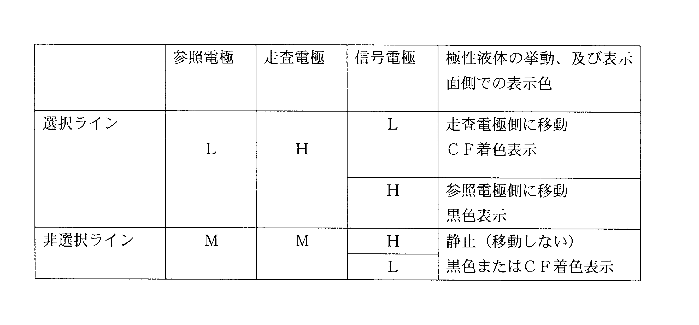
すなわち、参照ドライバ8及び走査ドライバ9は、例えば同図の左側から右側に向かう所定の走査方向で、参照電極5及び走査電極6に対して、選択電圧としてL電圧(第2の電圧)及びH電圧(第1の電圧)をそれぞれ順次印加して選択ラインとする走査動作を行う。また、この選択ラインでは、信号ドライバ7は外部からの画像入力信号に応じて、対応する信号電極4に対して、H電圧またはL電圧を信号電圧Vdとして印加する。
一方、非選択ライン、つまり残り全ての参照電極5及び走査電極6に対しては、参照ドライバ8及び走査ドライバ9は、非選択電圧としてM電圧を印加する。
<選択ラインでの動作>
選択ラインでは、信号電極4に対して例えばL電圧が印加されているときでは、参照電極5と信号電極4との間では、共にL電圧が印加されているので、これらの参照電極5と信号電極4との間には、電位差が生じていない。一方、信号電極4と走査電極6との間では、走査電極6に対して、H電圧が印加されているので、電位差が生じている状態となる。従って、極性液体16は、信号電極4に対して、電位差が生じている走査電極6側に表示用空間Sの内部を移動する。この結果、極性液体16は、図5(b)に例示したように、非有効表示領域P2側に移動した状態となり、オイル17を参照電極5側に移動させて、バックライト18からの照明光がカラーフィルタ部11rに達するのを許容する。これにより、表示面側での表示色は、カラーフィルタ部11rによる赤色表示(CF着色表示)の状態となる。また、表1に示した場合と同様に、隣接するRGBの3つの全画素において、CF着色表示が行われたときには、白色表示が行われる。
選択ラインでは、信号電極4に対して例えばL電圧が印加されているときでは、参照電極5と信号電極4との間では、共にL電圧が印加されているので、これらの参照電極5と信号電極4との間には、電位差が生じていない。一方、信号電極4と走査電極6との間では、走査電極6に対して、H電圧が印加されているので、電位差が生じている状態となる。従って、極性液体16は、信号電極4に対して、電位差が生じている走査電極6側に表示用空間Sの内部を移動する。この結果、極性液体16は、図5(b)に例示したように、非有効表示領域P2側に移動した状態となり、オイル17を参照電極5側に移動させて、バックライト18からの照明光がカラーフィルタ部11rに達するのを許容する。これにより、表示面側での表示色は、カラーフィルタ部11rによる赤色表示(CF着色表示)の状態となる。また、表1に示した場合と同様に、隣接するRGBの3つの全画素において、CF着色表示が行われたときには、白色表示が行われる。
一方、選択ラインにおいて、信号電極4に対してH電圧が印加されているときでは、参照電極5と信号電極4との間では、電位差が生じ、信号電極4と走査電極6との間には、電位差が生じていない。従って、極性液体16は、信号電極4に対して、電位差が生じている参照電極5側に表示用空間Sの内部を移動する。この結果、極性液体16は、図5(a)に例示したように、有効表示領域P1側に移動した状態となり、バックライト18からの照明光がカラーフィルタ部11rに達するのを阻止する。これにより、表示面側での表示色は、極性液体16による黒色表示(非CF着色表示)の状態となる。
<非選択ラインでの動作>
非選択ラインでは、信号電極4に対して例えばL電圧が印加されているときでは、極性液体16は現状の位置に静止した状態で維持されて、現状の表示色で維持される。すなわち、参照電極5及び走査電極6の双方に対して、M電圧が印加されているので、参照電極5と信号電極4との間の電位差及び走査電極6と信号電極4との間の電位差は、共に同じ電位差が生じるからである。この結果、表示色は、現状の黒色表示またはCF着色表示から変更されずに維持される。
非選択ラインでは、信号電極4に対して例えばL電圧が印加されているときでは、極性液体16は現状の位置に静止した状態で維持されて、現状の表示色で維持される。すなわち、参照電極5及び走査電極6の双方に対して、M電圧が印加されているので、参照電極5と信号電極4との間の電位差及び走査電極6と信号電極4との間の電位差は、共に同じ電位差が生じるからである。この結果、表示色は、現状の黒色表示またはCF着色表示から変更されずに維持される。
同様に、非選択ラインにおいて、信号電極4に対してH電圧が印加されているときでも、極性液体16は現状の位置に静止した状態で維持されて、現状の表示色で維持される。すなわち、参照電極5及び走査電極6の双方に対して、M電圧が印加されているので、参照電極5と信号電極4との間の電位差及び走査電極6と信号電極4との間の電位差は、共に同じ電位差が生じるからである。
以上のように、表2に示した場合でも、表1に示した場合と同様に、非選択ラインにおいては、信号電極4がH電圧及びL電圧のいずれかの電圧であっても、極性液体16は移動せずに、静止して、表示面側での表示色は変化しない。
一方、選択ラインにおいては、信号電極4への印加電圧に応じて、上述のように、極性液体16を移動させることができ、表示面側での表示色を変更させることができる。
また、本実施形態の画像表示装置1では、表1及び表2に示した印加電圧の組み合わせ以外に、信号電極4への印加電圧を、H電圧またはL電圧の2値だけではなく、これらのH電圧とL電圧との間の電圧を、表示面側に表示される情報に応じて変化させることもできる。すなわち、画像表示装置1では、信号電圧Vdを制御することにより、階調表示が可能となる。これにより、表示性能に優れた表示素子10を構成することができる。
以上のように構成された本実施形態の表示素子10では、上部基板(第1の基板)2において、構造体14がその上部基板2の表示用空間S側の表面2aの全面を覆うように、設けられている。これにより、本実施形態の表示素子10では、上記従来例と異なり、撥水膜12の密着性を容易に高めることができ、当該撥水膜12の剥離等の不具合の発生を防ぐことができる。すなわち、本実施形態では、上記従来例と異なり、極性液体16の移動速度の高速化を図ったときでも、不具合が生じるのを防ぐことができ、優れた信頼性を有する表示素子を構成することができる。
また、本実施形態の構造体14には、複数の各画素領域Pに応じて、表示用空間Sの内部を区切るように、設けられた第1及び第2のリブ部材14b、14cが含まれている。これにより、本実施形態では、隣接する画素領域P内に極性液体16が流入するのを容易に防ぐことができ、優れた表示品位を有する表示素子10を容易に構成することができる。
また、本実施形態では、上記設置工程において、所定の金型K1を用いて、構造体14が設けられているので、当該構造体14を精度よく設けることができる。
また、本実施形態の画像表示装置(電気機器)1では、極性液体16の移動速度の高速化を図ったときでも、不具合が生じるのを防ぐことができ、優れた信頼性を有する表示素子10が表示部に用いられているので、信頼性に優れた表示部を備えた高性能な画像表示装置(電気機器)1を容易に構成することができる。
また、本実施形態の表示素子10では、信号ドライバ(信号電圧印加部)7、参照ドライバ(参照電圧印加部)8、及び走査ドライバ(走査電圧印加部)9が信号電極4、参照電極5、及び走査電極6に対して、信号電圧Vd、参照電圧Vr、及び走査電圧Vsを印加するようになっている。これにより、本実施形態では、優れた表示品位を有するマトリクス駆動方式の表示素子10を容易に構成することができるとともに、各画素領域の表示色を適切に変更することができる。
[第2の実施形態]
図11(a)~図11(c)は、本発明の第2の実施形態にかかる表示素子での構造体の設置工程を説明する図である。図12(a)及び図12(b)は、それぞれ本発明の第2の実施形態にかかる表示素子での撥水膜の形成工程及び極性液体の充填工程を説明する図である。図において、本実施形態と上記第1の実施形態との主な相違点は、構造体の材料層として、紫外線硬化合成樹脂材料を用いるとともに、設置工程において、紫外線を照射することにより、構造体を設けた点である。なお、上記第1の実施形態と共通する要素については、同じ符号を付して、その重複した説明を省略する。
図11(a)~図11(c)は、本発明の第2の実施形態にかかる表示素子での構造体の設置工程を説明する図である。図12(a)及び図12(b)は、それぞれ本発明の第2の実施形態にかかる表示素子での撥水膜の形成工程及び極性液体の充填工程を説明する図である。図において、本実施形態と上記第1の実施形態との主な相違点は、構造体の材料層として、紫外線硬化合成樹脂材料を用いるとともに、設置工程において、紫外線を照射することにより、構造体を設けた点である。なお、上記第1の実施形態と共通する要素については、同じ符号を付して、その重複した説明を省略する。
つまり、図11(a)において、本実施形態の配置工程では、構造体14の材料層14Xとして、紫外線硬化合成樹脂材料が用いられており、この材料層14Xが上部基板2の表面2aの全面を覆うように配置されている。
そして、図11(b)及び図11(c)に示すように、上部基板2の表面2a上に構造体14を設ける設置工程が行われる。すなわち、この設置工程では、マスク部材M1、M2を用いたフォトリソグラフィ処理が行われることにより、構造体14の各部(被覆面14a、第1及び第2のリブ部材14b、14c)が形成される。具体的にいえば、図11(b)に示すように、紫外線が、マスク部材M1、M2を材料層14Xの上方に設置した状態で、材料層14X側から照射される。続いて、図11(c)に示すように、上部基板2の表面2aとは反対側の表面から紫外線を照射することにより、材料層14Xでは、同図11(c)に左斜め向きのハッチングで示した部分だけが紫外線によって硬化される。そして、同図11(c)に右斜め向きのハッチングで示した、硬化されていない部分を除去することにより、上部基板2の表面2a上に被覆面14a、第1及び第2のリブ部材14b、14cを含んだ構造体14を設けることができる。
次に、図12(a)に示すように、構造体14の表面上に撥水膜12を形成する形成工程が行われる。つまり、この形成工程では、構造体14の表面に対して、例えばフッ素系樹脂材をディッピング法によって塗布して、80℃で30分間焼成することにより、撥水膜12が形成される。撥水膜12の膜厚は、例えば60nmである。
続いて、図12(b)に示すように、上部基板2に対して、極性液体16を充填する充填工程が行われる。具体的にいえば、上部基板2において、第1及び第2のリブ部材14b、14cにて区画された各画素領域P内に対し、例えばディスペンサー装置またはインクジェット装置により、極性液体16を充填する。なお、この極性液体16の充填工程の前または後において、オイル17の充填工程が同様に行われる。
以上の構成により、本実施形態では、上記第1の実施形態と同様な作用・効果を奏することができる。また、本実施形態では、材料層14Xとして、紫外線硬化合成樹脂材料を用いるとともに、設置工程では、紫外線を照射することにより、構造体14が設けられてきる。これにより、構造体14を容易に設けることができる。
[第3の実施形態]
図13は、本発明の第3の実施形態にかかる表示素子における、表示面側から見た場合での上部基板側の要部構成を示す拡大平面図である。図14(a)は、図13に示した表示素子の1つの画素領域での要部構成を示す拡大平面図であり、図14(b)は、図14(a)のXIVb-XIVb線断面図である。図15(a)及び図15(b)は、それぞれ非CF着色表示時及びCF着色表示時における、図13に示した表示素子の要部構成を示す断面図である。
図13は、本発明の第3の実施形態にかかる表示素子における、表示面側から見た場合での上部基板側の要部構成を示す拡大平面図である。図14(a)は、図13に示した表示素子の1つの画素領域での要部構成を示す拡大平面図であり、図14(b)は、図14(a)のXIVb-XIVb線断面図である。図15(a)及び図15(b)は、それぞれ非CF着色表示時及びCF着色表示時における、図13に示した表示素子の要部構成を示す断面図である。
図において、本実施形態と上記第1の実施形態との主な相違点は、構造体に、絶縁性流体を移動させるための移動用空間を構成するためのレール部材を含めるとともに、界面張力が30mN/m以下である撥水性の高い合成樹脂材料を当該構造体に用いた点である。なお、上記第1の実施形態と共通する要素については、同じ符号を付して、その重複した説明を省略する。尚、図14では、図面の簡略化のために、カラーフィルタ層11、信号電極4、参照電極5、走査電極6、及び誘電体層13の図示は省略している。
つまり、図13~図15(b)に示すように、本実施形態の表示素子10では、上部基板2の表面2aに、構造体24が設けられている。この構造体24には、表面2aの全面を覆うように設けられた被覆面24aと、この被覆面24a上でY方向及びX方向にそれぞれ平行となるように設けられた第1のリブ部材24b及び第2のリブ部材24cを有する枠状のリブ(仕切壁)とが設けられている。また、これら第1及び第2のリブ部材24b、24cは、第1の実施形態のものと異なり、画素領域Pを気密に区切るようになっている。つまり、これら第1及び第2のリブ部材24b、24cは、互いに接続され、かつ、下部基板3側の端部は当該下部基板側に当接するようになっている。
また、構造体24には、上記枠状のリブ内で下部基板3側に突出するように設けられた複数、例えば4本のレール部材24dが含まれている。これら4本のレール部材24dは、互いに所定の間隔をおいて設けられており、オイル(絶縁性流体)17を移動させるための移動用空間を構成している。つまり、各レール部材24dは、図14(a)及び図14(b)に示すように、上部基板2側から表示用空間Sの内部側に突出するように、かつ、当該上部基板2側で有効表示領域P1と非有効表示領域P2とを接続するように直線状に設けられており、表示用空間Sの内部において、移動用空間Kを区画している。これにより、本実施形態の表示素子10では、例えば図14(b)に示すように、各画素領域Pにおいて、オイル(絶縁性流体)17を移動させるための移動用空間Kが、表示用空間Sの内部において、極性液体16が移動する空間の上部基板2側に形成される。
また、複数のレール部材24dは、例えば図15(a)及び図15(b)に示すように、移動用空間Kの内部において、一端部側及び他端部側がそれぞれ有効表示領域P1側及び非有効表示領域P2側に設けられるとともに、極性液体16の移動に応じて、オイル17を有効表示領域P1側または非有効表示領域P2側に案内するガイド部として機能するようになっている。また、各レール部材24dは、信号電極4、参照電極5、走査電極6、及び誘電体層13が設置された下部基板3側に設けられていないので、各レール部材24dは、エレクトロウェッティング現象による極性液体16の移動を阻害しないように構成されている。
また、複数のレール部材24dでは、図14(a)及び図14(b)に示すように、隣接する2本のレール部材24dの間の寸法h1、第1のリブ部材24bとレール部材24dとの間の寸法h2、及び第2のリブ部材24cとレール部材24dとの間の寸法h3が、各々上部基板2及び下部基板3と垂直な方向での極性液体16の寸法Hよりも小さい寸法に設定されている。具体的にいえば、本実施形態では、寸法h1~h3は各々例えば10μmに設定され、寸法Hは例えば40μmに設定されている。
以上のように、寸法Hよりも小さい寸法の寸法h1~h3を用いることにより、本実施形態では、極性液体16の動作(移動)が不安定になるのを防止することができる。すなわち、本願発明の発明者等による実験によれば、極性液体16が、隣接する2つのレール部材24dの間、第1のリブ部材24bとレール部材24dとの間、及び第2のリブ部材24cとレール部材24dとの間の各間に入り込むのを防ぐことができる。この結果、本実施形態では、極性液体16の動作が不安定になるのを防止することができる。尚、本願発明の発明者等による実験によれば、例えば隣接する2つのレール部材24dの間の寸法h1を、極性液体16の寸法H以上とした場合、極性液体16が当該隣接する2つのレール部材24dの間に入り込んで、極性液体16の動作が安定しなかった。
さらに、構造体24には、界面張力が30mN/m以下である撥水性の高い合成樹脂材料が用いられており、上記撥水膜12の設置が割愛されている。
ここで、図16を参照して、本実施形態の表示素子10の製造工程を具体的に説明する。尚、以下の説明では、第1の実施形態のものと異なる工程を主に説明する。
図16(a)~図16(c)は、図13に示した表示素子での構造体の設置工程を説明する図である。
図16(a)において、上部基板2の表面2aの全面を覆うように、構造体24を形成する材料層24Xを配置する配置工程が行われる。この材料層24Xには、例えばポリプロピレン(PP)、ポリメチルペンテン(TPX)、あるいはポリテトラフロロエチレン(PTFE)などの界面張力が30mN/m以下である撥水性の高い合成樹脂材料が用いられている。また、このような材料層24Xは、上記のように、界面張力が低いので、本実施形態の配置工程では、材料層24Xが、予め金型K3に流し込まれている。また、この金型K3には、構造体24に含まれた第1及び第2のリブ部材24b、24c、及びレール部材24dを形成するための溝K3a、K3b、及びK3cが予め設けられている。
そして、図16(b)に示すように、上部基板2の表面2aの全面を覆うように、構造体24を形成する材料層24Xを配置する配置工程が行われた後、引き続いて、上部基板2の表面2a上に構造体24を設ける設置工程が行われる。すなわち、配置工程において、材料層24Xが流し込まれた金型K3の上方から上部基板2の表面2aを重ね合わせることで、表面2a上に材料層24Xが配置される。その後、設置工程では、金型K3を用いた熱インプリント処理(例えば、温度140℃、圧力10MPa)が行われるようになっており、被覆面24a、第1及び第2のリブ部材24b、24c、及びレール部材24dが表面2a上に形成される。
次に、上部基板2及び構造体24が冷却された後、図16(c)に示すように、上部基板2及び構造体24は金型K3から離型されて、上部基板2側が完成される。
以上の構成により、本実施形態では、上記第1の実施形態と同様な作用・効果を奏することができる。また、本実施形態では、構造体24として、界面張力が30mN/m以下である撥水性の高い合成樹脂材料が用いられているので、第1の実施形態のものと異なり、撥水膜12の設置を割愛しつつ、構造体24によって極性液体16の移動速度を容易に向上させることができる。
また、本実施形態の構造体24には、画素領域P毎に設けられるとともに、オイル17を移動させるための移動用空間Kを構成するためのレール部材24dが含まれている。これにより、本実施形態では、極性液体16を移動させる場合において、当該極性液体16をより円滑に、かつ、より適切に移動させることができ、極性液体16の移動速度の高速化をより容易に図ることができる。
[第4の実施形態]
図17(a)及び図17(b)は、それぞれ非CF着色表示時及びCF着色表示時における、本発明の第4の実施形態にかかる表示素子の要部構成を示す断面図である。図において、本実施形態と上記第3の実施形態との主な相違点は、改質剤が添加された合成樹脂材料を構造体に用いた点である。なお、上記第3の実施形態と共通する要素については、同じ符号を付して、その重複した説明を省略する。
図17(a)及び図17(b)は、それぞれ非CF着色表示時及びCF着色表示時における、本発明の第4の実施形態にかかる表示素子の要部構成を示す断面図である。図において、本実施形態と上記第3の実施形態との主な相違点は、改質剤が添加された合成樹脂材料を構造体に用いた点である。なお、上記第3の実施形態と共通する要素については、同じ符号を付して、その重複した説明を省略する。
つまり、図17(a)及び図17(b)において、本実施形態の表示素子10では、上部基板2の表面2aに、構造体34が設けられている。この構造体34には、表面2aの全面を覆うように設けられた被覆面34aと、この被覆面34a上でY方向及びX方向にそれぞれ平行となるように設けられた第1のリブ部材34b及び第2のリブ部材34cを有する枠状のリブ(仕切壁)とが設けられている。また、これら第1及び第2のリブ部材34b、34cは、第3の実施形態のものと同様に、画素領域Pを気密に区切るようになっている。つまり、これら第1及び第2のリブ部材34b、34cは、互いに接続され、かつ、下部基板3側の端部は当該下部基板側に当接するようになっている。
また、構造体34には、第3の実施形態のものと同様に、上記枠状のリブ内で下部基板3側に突出するように設けられた複数、例えば4本のレール部材34dが含まれている。これら4本のレール部材34dは、互いに所定の間隔をおいて設けられており、オイル(絶縁性流体)17を移動させるための移動用空間を構成している。つまり、各レール部材34dは、図17(a)及び図17(b)に示すように、上部基板2側から表示用空間Sの内部側に突出するように、かつ、当該上部基板2側で有効表示領域P1と非有効表示領域P2とを接続するように直線状に設けられており、表示用空間Sの内部において、移動用空間を区画している。これにより、本実施形態の表示素子10では、第3の実施形態のものと同様に、各画素領域Pにおいて、オイル(絶縁性流体)17を移動させるための移動用空間が、表示用空間Sの内部において、極性液体16が移動する空間の上部基板2側に形成される。
また、構造体34には、改質剤が添加された合成樹脂材料が用いられており、この改質剤によって、構造体34は、界面張力が30mN/m以下である撥水性の高い材料に改質されている。
ここで、図18を参照して、本実施形態の表示素子10の製造工程を具体的に説明する。尚、以下の説明では、第1の実施形態のものと異なる工程を主に説明する。
図18(a)~図18(d)は、図17に示した表示素子での構造体の設置工程を説明する図である。
図18(a)において、材料層34Xを改質する改質工程が行われる。すなわち、この改質工程では、材料層34Xとしての合成樹脂材料に対し、改質剤を添加することにより、当該合成樹脂材料を、界面張力が30mN/m以下である撥水性の高い材料に改質することが行われる。具体的には、材料層34Xが、予め金型K4に流し込まれており、この材料層34Xに対して、改質剤を加えることによって、当該材料層34Xは、上記撥水性の高い材料に変えられている。より具体的には、例えばメタクリル樹脂(PMMA)に対して、フッ素系表面改質剤を添加することにより、材料層34Xは、界面張力が30mN/m以下である撥水性の高い材料に改質されている。
また、金型K4には、構造体34に含まれた第1及び第2のリブ部材34b、34c、及びレール部材34dを形成するための溝K4a、K4b、及びK4cが予め設けられている。
次に、図18(b)に示すように、上部基板2が、改質された材料層34Xの上方に、表面2aを下にした状態で、配置される。
そして、図18(c)に示すように、上部基板2の表面2aの全面を覆うように、構造体34を形成する材料層34Xを配置する配置工程が行われた後、引き続いて、上部基板2の表面2a上に構造体34を設ける設置工程が行われる。すなわち、配置工程において、材料層34Xが流し込まれた金型K4の上方から上部基板2の表面2aを重ね合わせることで、表面2a上に材料層34Xが配置される。その後、設置工程では、金型K4を用いた熱インプリント処理(例えば、温度140℃、圧力10MPa)が行われるようになっており、被覆面34a、第1及び第2のリブ部材34b、34c、及びレール部材34dが表面2a上に形成される。
次に、上部基板2及び構造体34が冷却された後、図18(d)に示すように、上部基板2及び構造体34は金型K4から離型されて、上部基板2側が完成される。
以上の構成により、本実施形態では、上記第3の実施形態と同様な作用・効果を奏することができる。また、本実施形態では、構造体34として、改質剤が添加されることにより、界面張力が30mN/m以下である撥水性の高い材料に改質された合成樹脂材料が用いられている。これにより、本実施形態では、改質剤によって、撥水膜12の設置を割愛しつつ、極性液体16の移動速度を容易に向上可能な構造体34を構成できる合成樹脂材料の種類などの選択肢を広げることができ、当該構造体34の設計自由度も広げることができる。
[第5の実施形態]
図19は、本発明の第5の実施形態にかかる表示素子における、表示面側から見た場合での上部基板側の要部構成を示す拡大平面図である。図20(a)及び図20(b)は、それぞれ非CF着色表示時及びCF着色表示時における、図19に示した表示素子の要部構成を示す断面図である。図において、本実施形態と上記第1の実施形態との主な相違点は、上部基板と構造体とを一体的に設けた点である。なお、上記第1の実施形態と共通する要素については、同じ符号を付して、その重複した説明を省略する。
図19は、本発明の第5の実施形態にかかる表示素子における、表示面側から見た場合での上部基板側の要部構成を示す拡大平面図である。図20(a)及び図20(b)は、それぞれ非CF着色表示時及びCF着色表示時における、図19に示した表示素子の要部構成を示す断面図である。図において、本実施形態と上記第1の実施形態との主な相違点は、上部基板と構造体とを一体的に設けた点である。なお、上記第1の実施形態と共通する要素については、同じ符号を付して、その重複した説明を省略する。
つまり、図19~図20(b)において、本実施形態の表示素子10では、上部基板22には、例えばメタクリル樹脂(PMMA)が用いられている。また、この上部基板22では、上部基板(第1の基板)として機能する基板本体22aと、この基板本体22aに一体的に設けられた構造体22bとが含まれている。また、構造体22bには、第1の実施形態のものと同様に、第1のリブ部材22c及び第2のリブ部材22dが含まれている。
ここで、図21~図22を参照して、本実施形態の表示素子10の製造工程を具体的に説明する。尚、以下の説明では、第1の実施形態のものと異なる工程を主に説明する。
図21(a)~図21(c)は、図19に示した表示素子での構造体の設置工程を説明する図である。図22(a)及び図22(b)は、それぞれ図19に示した表示素子での撥水膜の形成工程及び極性液体の充填工程を説明する図である。
図21(a)に示すように、上部基板22では、基板本体22aに材料層22Xが設けられており、この材料層22Xが、金型K1の上方となるように、配置される。
続いて、図22(b)に示すように、上部基板22の表面側に構造体22bを設ける設置工程が行われる。すなわち、この設置工程では、金型K1を用いた熱インプリント処理(例えば、温度140℃、圧力10MPa)が行われるようになっており、第1及び第2のリブ部材22c、22dが表面側に形成される。
その後、上部基板22が冷却された後、図21(c)に示すように、上部基板22は金型K1から離型される。そして、後続の形成工程の前に、構造体22bの表面に対して、所定のプライマー処理が行われる。
次に、図22(a)に示すように、構造体22bの表面、つまり第1及び第2のリブ部材22c、22dの表面、及び基板本体22aの第1及び第2のリブ部材22c、22dが形成されていない部分の表面上に撥水膜12を形成する形成工程が行われる。つまり、この形成工程では、上記構造体22bの表面に対して、例えばフッ素系樹脂材をディッピング法によって塗布して、80℃で30分間焼成することにより、撥水膜12が形成される。撥水膜12の膜厚は、例えば60nmである。また、上記プライマー処理を行うことにより、構造体22bの表面と撥水膜12との密着性の向上が図られている。
続いて、図22(b)に示すように、上部基板22に対して、極性液体16を充填する充填工程が行われる。具体的にいえば、上部基板22において、第1及び第2のリブ部材22c、22dにて区画された各画素領域P内に対し、例えばディスペンサー装置またはインクジェット装置により、極性液体16を充填する。なお、この極性液体16の充填工程の前または後において、オイル17の充填工程が同様に行われる。
以上の構成により、本実施形態では、上記第1の実施形態と同様な作用・効果を奏することができる。また、本実施形態では、上部基板22と構造体22bが一体的に設けられているので、部品点数が少なく製造簡単な表示素子10を容易に得ることができる。
尚、上記の説明以外に、例えば無アルカリガラス基板などの透明なガラス材を用いて、上部基板及び構造体を一体的に形成してもよい。また、上記第2の実施形態に示した紫外線硬化樹脂材料を用いて、上部基板及び構造体を一体的に形成したり、上記第3または第4の実施形態に示した撥水性の高い合成樹脂材料を用いて、上部基板及び構造体を一体的に形成したりする構成でもよい。
尚、上記の実施形態はすべて例示であって制限的なものではない。本発明の技術的範囲は特許請求の範囲によって規定され、そこに記載された構成と均等の範囲内のすべての変更も本発明の技術的範囲に含まれる。
例えば、上記の説明では、表示部を備えた画像表示装置に本発明を適用した場合について説明したが、本発明は文字及び画像を含んだ情報を表示する表示部が設けられた電気機器であれば何等限定されるものではなく、例えば電子手帳等のPDAなどの携帯情報端末、パソコンやテレビなどに付随する表示装置、あるいは電子ペーパーその他、各種表示部を備えた電気機器に好適に用いることができる。
また、上記の説明では、極性液体への電界印加に応じて、当該極性液体を移動させるエレクトロウェッティング方式の表示素子を構成した場合について説明したが、本発明の表示素子は、これに限定されるものではなく、外部電界を利用して、表示用空間の内部で極性液体を動作させることにより、表示面側の表示色を変更可能な電界誘導型の表示素子であれば何等限定されるものではなく、電気浸透方式、電気泳動方式、誘電泳動方式などの他の方式の電界誘導型表示素子に適用することができる。
但し、上記各実施形態のように、エレクトロウェッティング方式の表示素子を構成する場合の方が、極性液体を低い駆動電圧で高速に移動させることが可能となる。また、エレクトロウェッティング方式の表示素子では、極性液体の移動に応じて表示色が変更されており、液晶層などの複屈折材料を用いた液晶表示装置等と異なり、情報表示に使用される、バックライトからの光や外光の光利用効率に優れた高輝度な表示素子を容易に構成できる点でも好ましい。さらには、画素毎にスイッチング素子を設ける必要がないので、構造簡単で高性能なマトリクス駆動方式の表示素子を低コストで構成できる点でも好ましい。
また、上記の説明では、信号電極、走査電極、及び参照電極と、信号ドライバ(信号電圧印加部)、走査ドライバ(走査電圧印加部)、及び参照ドライバ(参照電圧印加部)とを用いた構成について説明した。しかしながら、本発明は、第1及び第2の基板の少なくとも一方側において、その基板の表示用空間側の表面の全面を覆うように、画素領域毎に、極性液体を駆動するための構造体を設けたものであれば何等限定されない。
具体的にいえば、複数の信号電極と複数の走査電極とを互いに交差するように、マトリクス状に設けるとともに、信号電極と走査電極との交差部単位に設けられた複数の画素領域毎に、スイッチング素子、例えば薄膜トランジスタ(TFT)を設置する。そして、薄膜トランジスタのゲートに走査電極を接続して走査電圧印加部から電圧印加を行うよう構成する。さらに、薄膜トランジスタのソースに信号電極を接続して信号電圧印加部から電圧印加を行うよう構成するとともに、画素領域毎に設けた画素電極に薄膜トランジスタのドレインを接続して信号電極からの電圧を供給することで極性液体の移動動作を行わせるよう構成するものでよい。
但し、上記の各実施形態のように、参照電極及び参照ドライバ(参照電圧印加部)を設ける場合の方が、スイッチング素子を画素領域毎に設けることなく、表示不良が生じるのを防ぐことができるマトリクス駆動方式の表示素子を構成することができる点で好ましい。
また、上記の説明では、バックライトを備えた透過型の表示素子を構成した場合について説明したが、本発明はこれに限定されるものではなく、拡散反射板などの光反射部を有する反射型や、前記光反射部とバックライトとを併用した半透過型の表示素子にも適用することができる。
また、上記の説明では、構造体として、リブ部材またはリブ部材及びレール部材を用いた場合について説明したが、本発明の構造体は画素領域毎に、極性液体を駆動するためのものであれば何等限定されない。
また、上記の説明では、構造体を上部基板(第1の基板)に設けた場合について説明したが、本発明の構造体は第1及び第2の基板の少なくとも一方側において、その基板の前記表示用空間側の表面の全面を覆うように設けられたものであればよく、構造体を下部基板(第2の基板)に設けたり、構造体の一部の部分及び残りの部分をそれぞれ第1及び第2の基板に設けたりする構成でもよい。
また、上記の説明では、塩化カリウムの水溶液を極性液体に用いた場合について説明したが、本発明の極性液体はこれに限定されるものではない。具体的にいえば、極性液体には、塩化亜鉛、水酸化カリウム、水酸化ナトリウム、アルカリ金属水酸化物、酸化亜鉛、塩化ナトリウム、リチウム塩、リン酸、アルカリ金属炭酸塩、酸素イオン伝導性を有するセラミックスなどの電解質を含んだものを使用することができる。また、溶媒には、水以外に、アルコール、アセトン、ホルムアミド、エチレングリコールなどの有機溶媒を使用することもできる。さらに、本発明の極性液体には、ピリジン系、脂環族アミン系、または脂肪族アミン系などの陽イオンと、フッ化物イオンやトリフラート等のフッ素系などの陰イオンとを含んだイオン液体(常温溶融塩)を使用することもできる。
また、本発明の極性液体には、導電性を有する導電性液体と、所定以上の比誘電率、好ましくは15以上の比誘電率を有する高誘電性を有する液体が含まれている。
但し、上記の各実施形態のように、所定の電解質を溶かした水溶液を極性液体に使用する場合の方が、取扱性に優れるとともに、製造が簡単な表示素子を容易に構成することができる点で好ましい。
また、上記の説明では、無極性のオイルを用いた場合について説明したが、本発明はこれに限定されるものではなく、極性液体と混じり合わない絶縁性流体であればよく、例えばオイルに代えて、空気、具体的には、ヘリウム、ネオン、アルゴン等の希ガスや窒素などを使用してもよい。また、オイルとして、シリコーンオイル、脂肪系炭化水素などを使用することができる。また、本発明の絶縁性流体には、所定以下の比誘電率、好ましくは5以下の比誘電率を有する流体が含まれている。
但し、上記の各実施形態のように、極性液体と相溶性がない無極性のオイルを用いた場合の方が、空気と極性液体とを用いる場合よりは、無極性のオイル中で極性液体の液滴がより移動し易くなって、当該極性液体を高速移動させることが可能となり、表示色を高速に切り換えられる点で好ましい。
また、上記の説明では、信号電極、参照電極、及び走査電極を下部基板(第2の基板)側に設けた場合について説明した。しかしながら、本発明は、極性液体と接触するように、表示用空間の内部に信号電極を設置し、かつ、極性液体及び互いに電気的に絶縁された状態で、参照電極及び走査電極を第1及び第2の基板の一方側に設けるものであればよい。具体的にいえば、例えば信号電極を第1及び第2の基板の中間部分に設けるとともに、参照電極及び走査電極を第1の基板側に設けてもよい。
また、上記の説明では、参照電極及び走査電極を有効表示領域側及び非有効表示領域側にそれぞれ設置した場合について説明したが、本発明はこれに限定されるものではなく、参照電極及び走査電極を非有効表示領域側及び有効表示領域側にそれぞれ設置してもよい。
また、上記の説明では、参照電極及び走査電極を下部基板(第2の基板)の表示面側の表面に設けた場合について説明したが、本発明はこれに限定されるものではなく、絶縁材料からなる上記第2の基板の内部に埋設した参照電極及び走査電極を用いることもできる。このように構成した場合には、第2の基板を誘電体層として兼用させることができ、当該誘電体層の設置を省略することができる。さらに、誘電体層を兼用した第1及び第2の基板上に信号電極を直接的に設け、表示用空間の内部に当該信号電極を設置する構成でもよい。
また、上記の説明では、透明な電極材料を用いて参照電極及び走査電極を構成した場合について説明したが、本発明は参照電極及び走査電極のうち、画素の有効表示領域に対向するように設置される一方の電極だけを透明な電極材料によって構成すればよく、有効表示領域に対向されない他方の電極には、アルミニウム、銀、クロム、その他の金属などの不透明な電極材料を使用することができる。
また、上記の説明では、帯状の参照電極及び走査電極を用いた場合について説明したが、本発明の参照電極及び走査電極の各形状はこれに何等限定されない。例えば透過型に比べて、情報表示に用いられる光の利用効率が低下する反射型の表示素子では、線状や網状などの光ロスが生じ難い形状としてもよい。
また、上記の説明では、信号電極に線状配線を用いた場合について説明したが、本発明の信号電極はこれに限定されるものではなく、網状配線などの他の形状に形成された配線も使用することができる。
また、上記の説明では、黒色に着色された極性液体及びカラーフィルタ層を用いて、RGBの各色の画素を表示面側に設けた場合について説明したが、本発明はこれに限定されるものではなく、複数の画素領域が、表示面側でフルカラー表示が可能な複数の色に応じてそれぞれ設けられているものであればよい。具体的には、RGB、シアン(C)、マゼンタ(M)、及びイエロー(Y)のCMY、またはRGBYCなどに着色された複数色の極性液体を用いることもできる。
また、上記の説明では、カラーフィルタ層を下部基板(第2の基板)の表示面側の表面に形成した場合について説明したが、本発明はこれに限定されるものではなく、第2の基板の非表示面側の表面や上部基板(第1の基板)側にカラーフィルタ層を設置することもできる。このように、カラーフィルタ層を用いる場合の方が、複数色の極性液体を用意する場合に比べて、製造簡単な表示素子を容易に構成できる点で好ましい。また、このカラーフィルタ層に含まれたカラーフィルタ部(開口部)及びブラックマトリクス部(遮光膜)により、表示用空間に対し、有効表示領域及び非有効表示領域をそれぞれ適切に、かつ、確実に設定することができる点でも好ましい。
本発明は、極性液体の移動速度の高速化を図ったときでも、不具合が生じるのを防ぐことができ、優れた信頼性を有する表示素子、その製造方法、及びその表示素子を用いた電気機器に対して有用である。
1 画像表示装置(電気機器)
2 上部基板(第1の基板)
2a (表示用空間側の)表面
3 下部基板(第2の基板)
3a (表示用空間側の)表面
4 信号電極
5 参照電極
6 走査電極
7 信号ドライバ(信号電圧印加部)
8 参照ドライバ(参照電圧印加部)
9 走査ドライバ(走査電圧印加部)
10 表示素子
11 カラーフィルタ層
11r、11g、11b カラーフィルタ部(開口部)
11s ブラックマトリクス部(遮光膜)
13 誘電体層
14 構造体
14a 被覆面
14b 第1のリブ部材
14c 第2のリブ部材
14X 材料層
16 極性液体
17 オイル(絶縁性流体)
24 構造体
24a 被覆面
24b 第1のリブ部材
24c 第2のリブ部材
24d レール部材
24X 材料層
34 構造体
34a 被覆面
34b 第1のリブ部材
34c 第2のリブ部材
34d レール部材
34X 材料層
22 上部基板(第1の基板)
22a 基板本体
22b 構造体
22c 第1のリブ部材
22d 第2のリブ部材
S 表示用空間
P 画素領域
P1 有効表示領域
P2 非有効表示領域
K1、K3、K4 金型
2 上部基板(第1の基板)
2a (表示用空間側の)表面
3 下部基板(第2の基板)
3a (表示用空間側の)表面
4 信号電極
5 参照電極
6 走査電極
7 信号ドライバ(信号電圧印加部)
8 参照ドライバ(参照電圧印加部)
9 走査ドライバ(走査電圧印加部)
10 表示素子
11 カラーフィルタ層
11r、11g、11b カラーフィルタ部(開口部)
11s ブラックマトリクス部(遮光膜)
13 誘電体層
14 構造体
14a 被覆面
14b 第1のリブ部材
14c 第2のリブ部材
14X 材料層
16 極性液体
17 オイル(絶縁性流体)
24 構造体
24a 被覆面
24b 第1のリブ部材
24c 第2のリブ部材
24d レール部材
24X 材料層
34 構造体
34a 被覆面
34b 第1のリブ部材
34c 第2のリブ部材
34d レール部材
34X 材料層
22 上部基板(第1の基板)
22a 基板本体
22b 構造体
22c 第1のリブ部材
22d 第2のリブ部材
S 表示用空間
P 画素領域
P1 有効表示領域
P2 非有効表示領域
K1、K3、K4 金型
Claims (19)
- 表示面側に設けられた第1の基板と、所定の表示用空間が前記第1の基板との間に形成されるように、当該第1の基板の非表示面側に設けられた第2の基板と、前記表示用空間に対し、設定された有効表示領域及び非有効表示領域と、前記表示用空間の内部で前記有効表示領域側または前記非有効表示領域側に移動可能に封入された極性液体とを具備し、前記極性液体を移動させることにより、前記表示面側の表示色を変更可能に構成された表示素子であって、
前記極性液体と接触するように、前記表示用空間の内部に設置されるとともに、所定の配列方向に沿って設けられた複数の信号電極、
前記有効表示領域側及び前記非有効表示領域側の一方側に設置されるように、前記極性液体に対して電気的に絶縁された状態で、前記第1及び第2の基板の一方側に設けられるとともに、前記複数の信号電極と交差するように設けられた複数の走査電極、
前記信号電極と前記走査電極との交差部単位に設けられた複数の画素領域、
及び
前記表示用空間の内部に前記画素領域毎に移動可能に封入されるとともに、前記極性液体と混じり合わない絶縁性流体を備え、
前記第1及び第2の基板の少なくとも一方側において、その基板の前記表示用空間側の表面の全面を覆うように、前記画素領域毎に、前記極性液体を駆動するための構造体を設けた、
ことを特徴とする表示素子。 - 前記構造体の表面上には、撥水膜が形成されている請求項1に記載の表示素子。
- 前記構造体として、界面張力が30mN/m以下である撥水性の高い合成樹脂材料が用いられている請求項1に記載の表示素子。
- 前記構造体として、改質剤が添加されることにより、界面張力が30mN/m以下である撥水性の高い材料に改質された合成樹脂材料が用いられている請求項1に記載の表示素子。
- 前記第1及び第2の基板の少なくとも一方と前記構造体とが、一体的に設けられている請求項1に記載の表示素子。
- 前記構造体には、前記複数の各画素領域に応じて、前記表示用空間の内部を区切るように、設けられたリブ部材が含まれている請求項1~5のいずれか1項に記載の表示素子。
- 前記構造体には、前記画素領域毎に設けられるとともに、前記絶縁性流体を移動させるための移動用空間を構成するためのレール部材が含まれている請求項1~6のいずれか1項に記載の表示素子。
- 前記複数の信号電極に接続されるとともに、前記複数の各信号電極に対して、前記表示面側に表示される情報に応じて、所定の電圧範囲内の信号電圧を印加する信号電圧印加部と、
前記複数の走査電極に接続されるとともに、前記複数の各走査電極に対して、前記極性液体が前記信号電圧に応じて、前記表示用空間の内部を移動するのを許容する選択電圧と、前記極性液体が前記表示用空間の内部を移動するのを阻止する非選択電圧との一方の電圧を印加する走査電圧印加部とを備えている請求項1~7のいずれか1項に記載の表示素子。 - 前記複数の画素領域が、前記表示面側でフルカラー表示が可能な複数の色に応じてそれぞれ設けられている請求項1~8のいずれか1項に記載の表示素子。
- 前記有効表示領域側及び前記非有効表示領域側の他方側に設置されるように、前記極性液体及び前記走査電極に対して電気的に絶縁された状態で、前記第1及び第2の基板の一方側に設けられるとともに、前記複数の信号電極と交差するように設けられた複数の参照電極と、
前記複数の参照電極に接続されるとともに、前記複数の各参照電極に対して、前記極性液体が前記信号電圧に応じて、前記表示用空間の内部を移動するのを許容する選択電圧と、前記極性液体が前記表示用空間の内部を移動するのを阻止する非選択電圧との一方の電圧を印加する参照電圧印加部とが設けられている請求項1~9のいずれか1項に記載の表示素子。 - 前記参照電極及び前記走査電極の表面上には、誘電体層が積層されている請求項10に記載の表示素子。
- 前記非有効表示領域は、前記第1及び第2の基板の一方側に設けられた遮光膜によって設定され、
前記有効表示領域は、前記遮光膜に形成された開口部によって設定されている請求項1~11のいずれか1項に記載の表示素子。 - 文字及び画像を含んだ情報を表示する表示部を備えた電気機器であって、
前記表示部に、請求項1~12のいずれか1項に記載の表示素子を用いたことを特徴とする電気機器。 - 表示面側に設けられた第1の基板と、所定の表示用空間が前記第1の基板との間に形成されるように、当該第1の基板の非表示面側に設けられた第2の基板と、前記表示用空間に対し、複数の画素領域毎に設定された有効表示領域及び非有効表示領域と、前記表示用空間の内部で前記有効表示領域側または前記非有効表示領域側に移動可能に封入された極性液体及び前記極性液体と混じり合わない絶縁性流体を具備し、前記極性液体を移動させることにより、前記表示面側の表示色を変更可能に構成された表示素子の製造方法であって、
前記第1及び第2の基板の少なくとも一方側において、その基板の前記表示用空間側の表面の全面を覆うように、前記画素領域毎に、前記極性液体を駆動するための構造体を形成する材料層を配置する配置工程と、
前記材料層に対して、所定の処理を施すことにより、前記第1及び第2の基板の少なくとも一方側の前記表面上に前記構造体を設ける設置工程と、
を備えていることを特徴とする表示素子の製造方法。 - 前記設置工程では、所定の金型を用いて、前記構造体が設けられている請求項14に記載の表示素子の製造方法。
- 前記材料層として、紫外線硬化合成樹脂材料を用いるとともに、
前記設置工程では、紫外線を照射することにより、前記構造体が設けられている請求項14に記載の表示素子の製造方法。 - 前記設置工程の後に、前記構造体の表面上に、撥水膜を形成する形成工程を行う請求項13~15のいずれか1項に記載の表示素子の製造方法。
- 前記配置工程において、前記材料層として、界面張力が30mN/m以下である撥水性の高い合成樹脂材料を用いるとともに、前記第1及び第2の基板の少なくとも一方側または所定の金型に当該合成樹脂材料を配置する請求項14に記載の表示素子の製造方法。
- 前記配置工程の前に、前記材料層としての合成樹脂材料に対し、改質剤を添加することにより、当該合成樹脂材料を、界面張力が30mN/m以下である撥水性の高い材料に改質する改質工程を行う請求項14に記載の表示素子の製造方法。
Applications Claiming Priority (2)
| Application Number | Priority Date | Filing Date | Title |
|---|---|---|---|
| JP2010-287790 | 2010-12-24 | ||
| JP2010287790 | 2010-12-24 |
Publications (1)
| Publication Number | Publication Date |
|---|---|
| WO2012086538A1 true WO2012086538A1 (ja) | 2012-06-28 |
Family
ID=46313810
Family Applications (1)
| Application Number | Title | Priority Date | Filing Date |
|---|---|---|---|
| PCT/JP2011/079171 Ceased WO2012086538A1 (ja) | 2010-12-24 | 2011-12-16 | 表示素子、製造方法、及び電気機器 |
Country Status (1)
| Country | Link |
|---|---|
| WO (1) | WO2012086538A1 (ja) |
Citations (5)
| Publication number | Priority date | Publication date | Assignee | Title |
|---|---|---|---|---|
| JPH06123897A (ja) * | 1992-10-13 | 1994-05-06 | Casio Comput Co Ltd | 表示装置 |
| JP2007147829A (ja) * | 2005-11-25 | 2007-06-14 | Brother Ind Ltd | 電気泳動表示媒体における隔壁及び基板の製造方法、及び、電気泳動表示媒体 |
| JP2007233200A (ja) * | 2006-03-02 | 2007-09-13 | Sharp Corp | 反射型表示素子、及びこれを用いた電気機器 |
| WO2010095301A1 (ja) * | 2009-02-20 | 2010-08-26 | シャープ株式会社 | 表示素子、及びこれを用いた電気機器 |
| JP2010276994A (ja) * | 2009-05-29 | 2010-12-09 | Ricoh Co Ltd | 表示素子 |
-
2011
- 2011-12-16 WO PCT/JP2011/079171 patent/WO2012086538A1/ja not_active Ceased
Patent Citations (5)
| Publication number | Priority date | Publication date | Assignee | Title |
|---|---|---|---|---|
| JPH06123897A (ja) * | 1992-10-13 | 1994-05-06 | Casio Comput Co Ltd | 表示装置 |
| JP2007147829A (ja) * | 2005-11-25 | 2007-06-14 | Brother Ind Ltd | 電気泳動表示媒体における隔壁及び基板の製造方法、及び、電気泳動表示媒体 |
| JP2007233200A (ja) * | 2006-03-02 | 2007-09-13 | Sharp Corp | 反射型表示素子、及びこれを用いた電気機器 |
| WO2010095301A1 (ja) * | 2009-02-20 | 2010-08-26 | シャープ株式会社 | 表示素子、及びこれを用いた電気機器 |
| JP2010276994A (ja) * | 2009-05-29 | 2010-12-09 | Ricoh Co Ltd | 表示素子 |
Similar Documents
| Publication | Publication Date | Title |
|---|---|---|
| US8698715B2 (en) | Display device and method for manufacturing the same | |
| JPWO2009078194A1 (ja) | 表示素子、及びこれを用いた電気機器 | |
| KR20050092786A (ko) | 디스플레이 디바이스 | |
| JP2009003017A (ja) | 表示素子、製造方法、及び電気機器 | |
| US20120326956A1 (en) | Display element, and electrical device using same | |
| WO2012026161A1 (ja) | 表示素子、及びこれを用いた電気機器 | |
| JP5113938B2 (ja) | 表示素子、及びこれを用いた電気機器 | |
| WO2010095301A1 (ja) | 表示素子、及びこれを用いた電気機器 | |
| WO2011074304A1 (ja) | 表示素子、及びこれを用いた電気機器 | |
| WO2012066970A1 (ja) | 表示素子、及びこれを用いた電気機器 | |
| WO2012002013A1 (ja) | 表示素子、及びこれを用いた電気機器 | |
| WO2010016309A1 (ja) | 表示素子、及びこれを用いた電気機器 | |
| WO2010095302A1 (ja) | 表示素子、及びこれを用いた電気機器 | |
| WO2012086538A1 (ja) | 表示素子、製造方法、及び電気機器 | |
| WO2011092892A1 (ja) | 表示素子、及びこれを用いた電気機器 | |
| WO2012098987A1 (ja) | 表示素子、及びこれを用いた電気機器 | |
| JP2013125131A (ja) | 表示素子、製造方法、及び電気機器 | |
| JP2014006412A (ja) | 表示素子、及びこれを用いた電気機器 | |
| WO2011033802A1 (ja) | 表示素子、及びこれを用いた電気機器 | |
| WO2010016304A1 (ja) | 表示素子、及びこれを用いた電気機器 | |
| WO2013108851A1 (ja) | 表示素子、及びこれを用いた電気機器 | |
| JP2013125130A (ja) | 表示素子、及びこれを用いた電気機器 | |
| WO2012137779A1 (ja) | 表示素子、製造方法、及び電気機器 | |
| WO2012060244A1 (ja) | 表示素子、及びこれを用いた電気機器 | |
| WO2013031532A1 (ja) | 表示素子、及びこれを用いた電気機器 |
Legal Events
| Date | Code | Title | Description |
|---|---|---|---|
| 121 | Ep: the epo has been informed by wipo that ep was designated in this application |
Ref document number: 11850596 Country of ref document: EP Kind code of ref document: A1 |
|
| NENP | Non-entry into the national phase |
Ref country code: DE |
|
| 122 | Ep: pct application non-entry in european phase |
Ref document number: 11850596 Country of ref document: EP Kind code of ref document: A1 |
|
| NENP | Non-entry into the national phase |
Ref country code: JP |