WO2012086498A1 - 開閉器 - Google Patents
開閉器 Download PDFInfo
- Publication number
- WO2012086498A1 WO2012086498A1 PCT/JP2011/078962 JP2011078962W WO2012086498A1 WO 2012086498 A1 WO2012086498 A1 WO 2012086498A1 JP 2011078962 W JP2011078962 W JP 2011078962W WO 2012086498 A1 WO2012086498 A1 WO 2012086498A1
- Authority
- WO
- WIPO (PCT)
- Prior art keywords
- power supply
- circuit
- switch
- load
- side terminal
- Prior art date
- Legal status (The legal status is an assumption and is not a legal conclusion. Google has not performed a legal analysis and makes no representation as to the accuracy of the status listed.)
- Ceased
Links
Images




Classifications
-
- H—ELECTRICITY
- H01—ELECTRIC ELEMENTS
- H01H—ELECTRIC SWITCHES; RELAYS; SELECTORS; EMERGENCY PROTECTIVE DEVICES
- H01H83/00—Protective switches, e.g. circuit-breaking switches, or protective relays operated by abnormal electrical conditions otherwise than solely by excess current
- H01H83/20—Protective switches, e.g. circuit-breaking switches, or protective relays operated by abnormal electrical conditions otherwise than solely by excess current operated by excess current as well as by some other abnormal electrical condition
- H01H2083/201—Protective switches, e.g. circuit-breaking switches, or protective relays operated by abnormal electrical conditions otherwise than solely by excess current operated by excess current as well as by some other abnormal electrical condition the other abnormal electrical condition being an arc fault
-
- H—ELECTRICITY
- H01—ELECTRIC ELEMENTS
- H01H—ELECTRIC SWITCHES; RELAYS; SELECTORS; EMERGENCY PROTECTIVE DEVICES
- H01H9/00—Details of switching devices, not covered by groups H01H1/00 - H01H7/00
- H01H9/50—Means for detecting the presence of an arc or discharge
-
- H—ELECTRICITY
- H02—GENERATION; CONVERSION OR DISTRIBUTION OF ELECTRIC POWER
- H02H—EMERGENCY PROTECTIVE CIRCUIT ARRANGEMENTS
- H02H1/00—Details of emergency protective circuit arrangements
- H02H1/0007—Details of emergency protective circuit arrangements concerning the detecting means
- H02H1/0015—Using arc detectors
Definitions
- the present invention relates to a switch that is inserted into a DC power supply line and opens and closes an electric circuit.
- Patent Document 1 discloses a switch (circuit breaker with an overheat prevention mounting) provided with an overheat detecting means such as a temperature sensor in the vicinity of a terminal and having a function of preventing a burning accident due to a rise in terminal temperature.
- Patent Document 2 discloses a switch (circuit breaker) in which a temperature to be compared with a terminal temperature is set to be equal to or lower than an allowable temperature of an electric wire.
- JP 62-8419 A Japanese Utility Model Publication No. 2-75941
- a gap is created between the terminal of the switch and the wire due to loosening of the terminal screw, etc., and when an arc (discharge) occurs, especially when a direct current flows through the switch, compared to when an alternating current flows,
- the arc may continue to be generated in a continuously large state without pulsation, and the temperature rises faster than the protective action by the temperature sensor etc., and the switch and the electric wire are burned out.
- the temperature sensor can detect the arc generated at the terminal of the switch with a time delay, but for example, against the occurrence of an arc between the terminal and the wire in another device connected to the switch Cannot be detected.
- the main present invention for solving the above-mentioned problems is a switch having a power supply side terminal connected to a DC power supply and a load side terminal to which power from the DC power supply is output, wherein the power supply side terminal and the load side terminal are provided.
- a contact that is inserted into the connecting electrical circuit and opens and closes the electrical circuit between the DC power supply and the load; an arc detection circuit that outputs an arc detection signal when arc discharge detected through the electrical circuit continues for a predetermined time; and And a tripping unit that opens the contact when an arc detection signal is generated.
- the present invention it is possible to protect the switch and the device on the electric circuit to which the switch is connected from overheating due to the generation of an arc, and to suppress a burnout accident on the electric circuit to which the switch is connected.
- the switch 1 is connected between the solar cell module 2 and the power conditioner 3.
- the switch 1 opens and closes an electric circuit between the solar cell module 2 and the power conditioner 3.
- the solar cell module 2 is composed of a plurality of solar cell elements (cells) connected in series.
- the solar cell module 2 converts sunlight energy into electric energy by the photovoltaic effect and outputs it as DC power.
- the DC power is supplied to the power conditioner 3 via the switch 1. Further, the power conditioner 3 converts the DC power into AC power, superimposes it on the commercial AC power supply 5 and supplies it to the load 4.
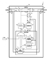
- the switch 1 shown in FIG. 2 includes a control circuit 10, temperature sensors 21 to 24, a power supply circuit 25, a tripping unit 26, contacts 31 to 34, and power supply lines L1 to L6.
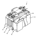
- the control circuit 10 is mounted on a substrate 15 and includes, for example, an overheat detection circuit 11, an arc detection circuit 12, a reverse connection detection circuit 13, and an OR circuit (OR circuit) 14 that detect a temperature rise. ing. And these have the external shape as shown in FIG.3, FIG5 and FIG.6, and the terminals 41 thru
- the housing 50 includes outer members 51 and 52 and inner members 53 and 54.
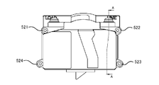
- the outer members 51 and 52 and the inner members 53 and 54 are provided with openings 511 to 514, 521 to 524, 531 to 534, and 541 to 544 for screwing at four corners, respectively.
- Female threads are provided in the openings 511 to 514 of the outer member 51.
- a male screw (not shown) is inserted from the openings 521 to 524 of the outer member 52 and is screwed with a female screw provided in the openings 511 to 514 of the outer member 51, and the outer member 51, the inner members 53 and 54, and the outer side.
- the member 52 is integrated.
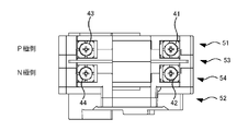
- Terminals 41 to 44 are provided on the upper surface of the casing 50.
- the terminals 41 and 42 are a pair of power supply side terminals on the positive side and the negative side, respectively.
- the solar cell module 2 power supply
- the terminals 43 and 44 are a pair of load side terminals on the positive side and the negative side, respectively, for example, to which a power conditioner 3 (load) is connected and can output DC power from the solar cell module 2.
- load side indicates the side closer to the load side terminals 43 and 44
- power supply side indicates the side closer to the power supply side terminals 41 and 42.
- the contact 31 is a positive contact, and one end is connected to the terminal 41 via the power line L1 and the other end is connected to the terminal 43 via the power line L3.
- the contact 32 is a negative contact, and one end is connected to the terminal 42 via the power supply line L2, and the other end is connected to the terminal 44 via the power supply line L4.
- the trip unit 26 is composed of a positive side assembly and a negative side assembly.
- the positive side assembly includes a coil 61 and an arm 62, and when the internal power is supplied to the coil 61, the arm 62 is driven via the link 63 to open the contact 31.
- the negative side assembly includes a coil, an arm 65, and a link in the same manner as the positive side assembly.
- the inner member 53 is formed with central internal sections 57 and 58 at the central portions of the positive and negative surfaces, respectively, and on the power source side with respect to the central internal sections 57 and 58, the positive power source internal section 59 and A negative power supply side internal section 60 is formed.
- the positive side power supply side internal section 59 and the negative side power supply side internal section 60 are collectively referred to, they are referred to as a power supply side internal section 93.
- the contact 31 is disposed in the positive central interior section 57 and the contact 32 is disposed in the negative central interior section 58.
- the coil 61 is disposed in the positive power supply side internal section 59, and the negative side power supply internal section 60 is disposed with the coil of the negative assembly.
- the positive-side central internal section 57 and the negative-side central internal section 58 are collectively referred to as a central internal section 92.
- a load-side internal section 91 for housing is formed.
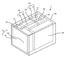
- FIG. 10 the schematic diagram of the switch of a present Example is shown.
- dotted lines indicate sections formed in the housing 50.
- the switch 1 has a substantially rectangular parallelepiped shape (can be approximated by a rectangular parallelepiped shape), and the lower part of the surface of the housing where the load-side terminals 43 and 44 are disposed (with the housing 50 sandwiched).
- a load side internal section is provided in the housing 50.
- a power supply side internal section 93 is disposed below the surface of the housing where the power supply terminals 41 and 42 are disposed.
- a load-side internal section 91, a central internal section 92, and a power-supply-side internal section 93 are arranged in order, and the control circuit housing section 94 includes a load-side internal section 91 and a central internal section.
- control circuit housing section 94 (substrate 15) is disposed adjacent to the load side internal section 91 and the power supply side internal section 93 disposed below the terminals 41 to 44, the housing in which the terminals 41 to 44 are disposed. It will be arranged in the lower part of the position of the housing surface which is shifted from the position of the surface.
- the electric paths 95 and 96 connecting the power supply side terminals 41 and 42 and the load side terminals 43 and 44 are the load side internal section 91, the central internal section 92, the power supply side internal section 93, and the control circuit accommodating section 94.
- the load side internal section 91, the central internal section 92, and the power supply side internal section 94 are disposed through at least one of the inside and the top.
- the contacts 33 and 34 are auxiliary contacts, each having one end connected to the power supply lines L3 and L4 and the other end connected to the power supply circuit 25 via the power supply lines L5 and L6, respectively.
- the contact 33 is disposed in the control circuit accommodating section 94.
- the contact 34 is opened by driving an auxiliary arm 73 (opening mechanism).
- the auxiliary arm 73 is linked to the arm 65 through the opening 70 provided in the inner member 54 and interlocks with the operation of the arm 65. That is, when the trip unit 26 operates and the contact 32 is opened, the contact 34 is also opened by the interlocking of the auxiliary arm 73.
- the contact 33 is opened by driving an auxiliary arm that is interlocked with the arm 62.
- auxiliary contact can be either the contact 33 or 34.
- the contact 33 is omitted, and only the contact 34 is connected to the power supply line L4 on the load side at one end, and connected to the power supply circuit 25 through the power supply line L6.
- the power supply circuit 25 generates an internal power supply to be supplied to the trip unit 26 and the control circuit 10.
- the power supply circuit 25 is supplied with the voltage between the power supply lines L5 and L6, that is, the (external) power supply voltage V0 input between the terminals 41 and 42.
- the internal power supply voltage V1 output from the power supply circuit 25 is supplied to the control circuit 10. Further, the internal power supply voltage V2 output from the power supply circuit 25 is supplied to the trip unit 26.
- the inner members 53 and 54 are provided with openings 55 and 56, and the load-side internal section 91 is formed by the openings 55 and 56 and the outer members 51 and 52.
- a substrate 27 on which the power supply circuit 25 is mounted is disposed in the load side internal section 91.
- the board 27 is arranged on the load side with respect to the board 15 on which the control circuit 10 is mounted and the trip unit 26.
- slits 81 and 82 (concave portions) are formed at the inner end portions of the upper and lower surfaces of the openings 55 and 56 of the inner members 53 and 54, respectively. Is provided.
- the slit 82 on the lower surface is provided only on the inner member 53.
- the temperature sensors 21 to 24 are semiconductor temperature detection elements such as thermistors, and are arranged in the vicinity of the terminals 41 to 44, respectively, so that the temperature of the terminals or the temperature around the terminals can be measured.
- the currents corresponding to the measured temperatures T1 to T4 output from the temperature sensors 21 to 24 are input to the overheat detection circuit 11 and recognized as the measured temperatures T1 to T4.
- the overheat detection circuit 11 is set in advance.
- the overheat detection signal OH is output based on the following conditions.
- the overheat detection circuit 11 detects an overheat state in which any of the measured temperatures T1 to T4 is equal to or higher than a temperature (predetermined temperature) set according to the allowable temperature of the electric wire connected to each terminal, and detects overheat.
- the signal OH is output.
- the overheat detection circuit 11 uses a comparator or the like to generate an overheat detection signal OH that is low level when each measured temperature is lower than a predetermined temperature, and is high level when the measured temperature is higher than a predetermined temperature. Output.
- the predetermined voltage is set to about 100 ° C. as an example.
- the overheat detection circuit 11 preferably sets the overheat detection signal OH to a high level when the overheat state continues for a predetermined time or more.
- the overheat detection circuit 11 When the overheat detection circuit 11 is constituted by a microcomputer or the like, the current value output from the temperature sensors 21 to 24 is taken as a digital value from an A / D (analog / digital) conversion port, and the digital value and Comparison is made with a set value (digital value corresponding to a predetermined voltage), and the output port of the overheat detection signal OH is set to high level.
- the arc detection circuit 12 detects the occurrence of an arc in the electric circuit to which the switch 1 is connected. As shown in FIG. 9, the arc detection circuit 12 outputs a signal when detecting a state in which arc discharge continues, and includes a fluctuation detection circuit 121, counter circuits 122 and 123, and a determination circuit 124. It is configured to include. Further, the fluctuation detection circuit 121 includes, for example, capacitors C1 and C2 and an amplifier circuit A1.
- the input terminal of the amplifier circuit A1 is capacitively coupled to the power supply line L5 via a (coupling) capacitor C1, and passes an AC voltage superimposed on the DC voltage.
- the output terminal of the amplifier circuit A1 is capacitively coupled to the counter circuit 122 via a (coupling) capacitor C2, cuts off the DC voltage used for the bias in the amplifier circuit A1, and is shaped into a rectangular waveform by the amplifier circuit A1.
- the fluctuation voltage is output as a fluctuation detection signal AC0.
- the fluctuation detection circuit 121 of the arc detection circuit 12 amplifies the fluctuation of the power supply voltage V0 input via the capacitor C1 by the amplifier circuit A1, and further outputs it as a fluctuation detection signal AC0 via the capacitor C2.
- the amplifier circuit A1 adjusts the level of the fluctuation detection signal AC0 according to the logic level of the counter circuit 122.
- the fluctuation detection signal AC0 output from the fluctuation detection circuit 121 is input to CK (clock input). Further, the counter circuit 122 changes its output when the counter value exceeds a predetermined number of times within a predetermined time (about 10 ms as an example) controlled by a clock CLK input to CL (clear input). The output of the terminal is output as the full count signal AC1. Further, the full count signal AC1 is input to the counter circuit 123 (second counter unit), and the counter circuit 123 counts the full count signal AC1. The count value CNT output from the counter circuit 123 is input to the determination circuit 124, and the arc detection signal ARC is output from the determination circuit 124.
- the average frequency of the AC component superimposed on the DC power is divided by the counter circuit 122 and the dispersion of the arc discharge frequency is averaged and counted, and a value corresponding to the time of the full count interval of this count is the count value CNT.
- the counter circuit 122 counts based on the number of pulsations of the fluctuation detection signal AC0, and the count value increases.
- the counter circuit 122 is a 12-bit binary counter, for example, and starts counting from 0 to 4095 each time the clock CLK is input to CL. Then, the counter circuit 122 outputs, as the full count signal AC1, an output of a terminal whose output changes when the count value reaches a predetermined number or more, for example, a 12th bit terminal.
- the counter circuit 123 counts the full count signal AC1 from the counter circuit 122 within a predetermined time, and the count value CNT increases.
- the predetermined time similarly to the counter circuit 122, it is set to about 10 ms by the clock CLK input to the CL input. That is, the number of times the counter circuit 122 counts a predetermined number of times within a predetermined time is counted.
- the determination circuit 124 When the count value CNT immediately before being cleared is within a predetermined range, the determination circuit 124 outputs an arc detection signal ARC that arc discharge has occurred.
- the fluctuation of the power supply voltage V0 when an arc is generated in the electric circuit between the solar cell module 2 and the power conditioner 3 includes a high-frequency component of about several MHz.
- the determination circuit 124 has a count value CNT (immediately before clearing) of 2 (first). 1), the arc detection signal ARC is set to the high level. As an example, if the occurrence of an arc is detected by a fluctuation component of 1 MHz to 10 MHz, the determination circuit 124 determines that the arc is generated when the count value CNT in the 10 ms period is 2 or more and 25 (second reference value) or less. The detection signal ARC is set to the high level. Note that the determination circuit 124 preferably sets the arc detection signal ARC to a high level when the count value CNT for a period of 10 ms is continuously within a predetermined range for a predetermined time (a plurality of times).
- the arc detection circuit 12 detects the occurrence of an arc in the electric circuit to which the switch 1 is connected, and outputs an arc detection signal ARC.
- the reverse connection detection circuit 13 receives the power supply voltage V0, and the reverse connection detection circuit 13 outputs a reverse connection detection signal RC when the polarities of the DC power supplies connected to the terminals 41 and 42 are reversed.
- the reverse connection detection circuit 13 detects a reverse connection state in which a power source whose negative side (terminal 42) has a higher potential than the positive side (terminal 41) is connected to the terminals 41 and 42 which are power source side terminals.
- the reverse connection detection signal RC is output.
- the reverse connection detection circuit 13 is configured by a photocoupler, and the anode side of the primary side light emitting diode is connected to the terminal 42 (negative side), and the voltage at the terminal 42 is higher than the voltage at the terminal 41. In the reverse connection state, the light emitting diode emits light, the secondary phototransistor is turned on, and the high level reverse connection detection signal RC is output.
- the OR determination unit 14 receives the overheat detection signal OH, the arc detection signal ARC, and the reverse connection detection signal RC, and also receives the control signal CON via the terminal 45. Further, the trip command signal OP output from the OR determination unit 14 is input to the trip unit 26 to open the contacts 31 and 32, thereby preventing DC power from being output from the switch.
- the substrate 15 on which the control circuit 10 including the overheat detection circuit 11, the arc detection circuit 12, and the reverse connection detection circuit 13 is mounted is disposed in a control circuit housing section 94 formed inside the outer member 52.
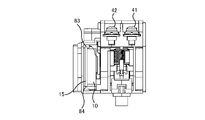
- the control circuit accommodating section 94 is adjacent to the load side internal section 91 and communicates with the load side internal section 91.
- the substrate 15 is arranged on the power supply side with respect to the substrate 27 on which the power supply circuit 25 is mounted.
- the substrate 15 is held inside a curved holder 80 (arm member), and the end of the holding portion 80 is fixed to the inner member 54.
- FIG. 8 which is an AA cross-sectional view of FIG.
- the holder 80 is provided with slits 83 and 84 (concave portions) for holding the substrate 15, and the substrate 15 is slid into the slits 83 and 84. By doing so, the substrate 15 is attached to the holder 80.
- a wall 71 is provided between the central internal section 92 and the power supply side internal section 93 and the control circuit housing section 94 (substrate 15).
- a wall may also be provided between the load side internal section 91 and the control circuit housing section 94.
- the power supply circuit 25 uses the internal power supply voltages V1 and V2 when the power supply voltage V0 is equal to or lower than a voltage (predetermined voltage) necessary for generating the internal power supply voltage V2 for operating the trip unit 26. Shall not be generated.
- the predetermined voltage is set according to the configuration of the power supply circuit 25 and the trip unit 26, and is set to about 50V as an example.
- the OR determination unit 14 In addition to the overheat detection signal OH, the arc detection signal ARC, and the reverse connection detection signal RC, the OR determination unit 14 also receives a control signal CON for opening the contacts 31 to 34.
- the OR determination unit 14 sets the trip command signal OP to a high level when the control signal CON, the overheat detection signal OH, the arc detection signal ARC, or the reverse connection detection signal RC becomes a high level.
- the trip command signal OP becomes a high level, the trip unit 26 opens the contacts 31 and 32 and also opens the contacts 33 and 34 in conjunction therewith.
- the switch 1 performs tripping when a control signal CON is input from the outside, when an overheat state is detected, when an arc is detected, or when a reverse connection state is detected, It protects the switch and the load connected to the switch.
- the branch point to the power supply circuit 25 is arranged on the power supply lines L3 and L4 on the load side from the contacts 31 and 32, when the contacts 31 and 32 are opened, the power supply lines L1 to L4 are connected.
- the power supplied from the solar cell module 2 (DC power supply) to the power supply circuit 25 can be cut off while being cut off.
- the auxiliary contacts 33 and 34 are provided on the line branched from the branch point to the power supply circuit 25 to the power supply circuit 25 side, the power supply circuit 25 flows backward from the power conditioner 3 (load). The power supplied to can also be cut off.
- the switch 1 when the control signal CON is input from the outside, the overheat state is detected, or the occurrence of an arc is detected, the tripping is performed by performing tripping.
- the load connected to 1 can be protected from overheating due to arcing, and a burnout accident on the electric circuit to which the switch 1 is connected can be prevented.
- the power supply circuit 25 since power is supplied to the power supply circuit 25 from the power supply lines L3 and L4 between the contacts 31 and 32 and the load side terminals 43 and 44, when the contacts 31 and 32 are opened, It is possible to prevent power from being supplied to the circuit 25. Therefore, when the contacts 31 and 32 of the switch 1 are opened, unnecessary power is not supplied to the power circuit 25, so that malfunction of the power circuit can be prevented. Further, since the power supply circuit 25 is disposed in the load-side internal section 91 provided on the load side in the housing 50, it is possible to shorten the wiring route from the branch point. Thereby, the assembly property of the switch 1 can be improved.
- the auxiliary contact is opened by the auxiliary arm that is linked to the tripping unit 26, so that the connection between the power supply lines L3 and L4 and the power supply circuit 25 is also disconnected. can do. Thereby, when tripping is performed, it is possible to prevent the power flowing back from the load side from being supplied to the power supply circuit 25.
- the control circuit 10 is disposed below the position of the housing surface that is shifted from the position of the housing surface where the terminals 41 to 44 are disposed, so that the arc is generated at the terminals 41 to 44. A situation where the arc directly affects the control circuit 10 can be avoided.
- the burnout propagates from the vicinity of the occurrence point, so the time until the control circuit 10 burns out is extended, and thus the control circuit 10 is pulled more reliably.
- the removal unit 26 can be operated.
- the electric paths 95 and 96 connecting the terminals 41 and 42 and the terminals 43 and 44 are the load side internal section 91 among the load side internal section 91, the central internal section 92, the power supply side internal section 93 and the control circuit accommodating section 94. Since the central internal section 92 and the power supply side internal section 93 are disposed through at least one of the inside and the top, the electric paths 95 and 96 are not disposed adjacent to the control circuit 10. Therefore, it is possible to avoid a situation that directly affects the control circuit 10 when an arc occurs in the electric circuit.
- the wall 71 is provided between the central internal section 92 and the power supply side internal section 93 and the control circuit accommodating section 94, the power supply terminals 41 and 42, the power supply lines L1 and L2, the contacts 31 and 32, the power supply It is possible to further reduce the influence of the arc generated in the electric circuit passing through the lines L3 and L4 and the load side terminals 43 and 44 on the control circuit 10. Further, the influence on the control circuit 10 such as an arc generated when the tripping unit 26 is operated can be reduced.
- the load-side internal section 91 and the control circuit housing section 94 communicate adjacent to each other, the power circuit 25 disposed in the load-side internal section 91 is connected to the control circuit 10 disposed in the control circuit housing section 94. Wiring can be performed easily.
- the power supply circuit 25 is configured as a circuit different from the control circuit 10 and is mounted on a substrate 27 different from the control circuit 10, the size of the power supply circuit 25 can be reduced.
- the output from the solar cell module 2 has a large voltage fluctuation range, for example, 0 V to 450 V, and the power supply circuit 25 requires a large circuit such as a stabilized power supply using a switching circuit.
- the size of the circuit 25 becomes relatively large, and the housing 50 needs to be enlarged to accommodate the power supply circuit 25.
- the control circuit 10 is not the same circuit as the power supply circuit 10 and is not mounted on the same substrate 27. With this configuration, the size of the power circuit 25 can be reduced, and the switch 1 can be downsized.
- the power supply circuit 25 normally generates heat
- the influence of heat generation from the power supply circuit 25 can be reduced by arranging the control circuit 10 in a control circuit housing section different from the power supply circuit 25.
- the board 27 is inserted and fixed in slits 81 and 82 formed on the upper and lower surfaces of the load side internal section, it is not necessary to use parts such as screws for fixing the board 27, and the number of parts is reduced. Can do. Further, the power supply circuit 25 can be disposed in the load side internal section by simply sliding the substrate 27 along the slits 81 and 82. Therefore, the assembly property of the switch 1 can be improved.
- the control circuit 10 can be arranged in the control circuit housing section simply by sliding the substrate 15 along the slits 83 and 84. Therefore, the assembly property of the switch 1 can be improved.
- the counter circuit 122 when the counter circuit 122 counts based on the fluctuation detection signal AC0 indicating the fluctuation of the power supply voltage V0, the state in which the counter circuit 122 counts a predetermined number of times or more in a predetermined time continues continuously for a certain time. In this case, the occurrence of the arc can be detected by the high frequency component included in the fluctuation of the power supply voltage V0 caused by the occurrence of the arc.
- the counter circuit 122 when the counter circuit 122 counts the full count signal AC1 indicating that the counter circuit 122 has counted a predetermined number of times within a predetermined time, the state where the count value CNT is equal to or greater than the first reference value continues for a certain period of time.
- the occurrence of an arc can be detected by the high frequency component included in the fluctuation of the power supply voltage V0.
- the arc detection signal ARC is output, whereby the arc can be detected by a component in a predetermined frequency band included in the fluctuation of the power supply voltage V0. The occurrence can be detected.
- any one of the measured temperatures T1 to T4 of the terminals 41 to 44 is continuously higher than a predetermined temperature (for example, 100 ° C.) for a predetermined time or longer, an overheat detection signal OH is output, thereby causing noise.
- a predetermined temperature for example, 100 ° C.
- the influence of temporary temperature fluctuations can be suppressed, and the overheat state can be detected more reliably.
- the power supply circuit 25 may generate the internal power supply voltage V2 necessary for performing the tripping by not generating the internal power supply voltages V1 and V2. If this is not possible, the operation of the control circuit 10 and the trip unit 26 can be stopped.
- a predetermined voltage for example, 50V
- reverse connection detection signal RC when reverse connection detection signal RC is input, it is possible to prevent reverse voltage / current from being supplied to the load connected to switch 1 by performing tripping.
- the switch 1 is used in a solar power generation system as an application example, but the present invention is not limited to this.
- the switch 1 can be widely used for distributed (type) power sources such as small-scale power generation facilities using other natural energy and cogeneration facilities.
- distributed (type) power sources such as small-scale power generation facilities using other natural energy and cogeneration facilities.
- an arc also occurs in an AC circuit, it is possible to detect the occurrence of an arc in an AC circuit by detecting a voltage fluctuation at a frequency higher than the commercial power supply frequency using a high-pass filter or the like.
- the switch 1 By configuring the switch 1 as an AC switch, it can be widely used for other applications. In the AC switch, the reverse connection detection circuit 13 is not used.
- the tripping unit 26 opens the contacts 31 to 34 when the control signal CON, the overheat detection signal OH, the arc detection signal ARC, or the reverse connection detection signal RC becomes high level. It is not limited to this. Some of these signals may be input to the OR circuit 14 that outputs the trip command signal OP, or other signals may be input.
- the outer members 51 and 52 and the inner members 53 and 54 constituting the casing 50 are integrated by screwing, but the present invention is not limited to this.
- the outer members 51 and 52 and the inner members 53 and 54 may be fixed by rivets.
Landscapes
- Breakers (AREA)
- Protection Of Static Devices (AREA)
Abstract
【課題】 開閉器や開閉器が接続された電路上の機器をアークの発生による過熱から保護し、開閉器が接続された電路上での焼損事故を防止する。 【解決手段】 直流電源につながる電源側端子と直流電源からの電力が出力される負荷側端子とを有する開閉器において、電源側端子と負荷側端子とをつなぐ電路に挿入され、直流電源と負荷との間の電路を開閉する接点と、電路を介して検出するアーク放電が所定時間継続した際にアーク検出信号を出力するアーク検出回路と、アーク検出信号が生成された場合に、接点を開極する引き外しユニットと、を有する。
Description
本発明は、直流電源ラインに挿入され電路の開閉を行う開閉器に関する。
開閉器の端子に電線を端子ねじで締め付けて配線する場合、端子ねじの締め付けトルクの不足や温度変化による熱膨張などによって端子ねじの締め付けにゆるみが生じ、端子ねじと電線との接触抵抗が増大して発熱する場合がある。そのため、端子温度が高くなった場合に接点を開極する切動作(引き外し)を行って電路を開く過熱保護機能を備えた開閉器もある。
例えば、特許文献1では、端子近傍に温度センサ等の過熱検知手段を備え、端子温度の上昇による焼損事故を未然に防止する機能を備えた開閉器(過熱防止装着付回路遮断器)が開示されている。また、例えば、特許文献2では、端子の温度と比較する温度を電線の許容温度以下に設定した開閉器(回路しゃ断器)が開示されている。
このように、端子の温度が所定の温度以上であることを検出した場合に引き外しを行うことによって、開閉器や当該開閉器に接続される電線の焼損を防止することができる。
しかしながら、端子ねじのゆるみなどによって開閉器の端子と電線との間に隙間ができ、アーク(放電)が発生すると、特に開閉器に直流電流が流れる場合には交流電流が流れる場合に比べて、その大きさが脈動することなく連続して大きい状態でアークが発生し続ける場合があり、温度センサなどによる保護動作が成されるよりも早く温度が上昇し、開閉器や電線が焼損してしまう場合もある。また、温度センサでは開閉器の端子に生じるアークを時間遅れを有して検知することができるが、例えば開閉器に接続された別の機器における端子と電線との間でのアーク発生に対しては検知することができない。
前述した課題を解決する主たる本発明は、直流電源につながる電源側端子と前記直流電源からの電力が出力される負荷側端子とを有する開閉器において、前記電源側端子と前記負荷側端子とをつなぐ電路に挿入され、前記直流電源と負荷との間の電路を開閉する接点と、前記電路を介して検出するアーク放電が所定時間継続した際にアーク検出信号を出力するアーク検出回路と、前記アーク検出信号が生成された場合に、前記接点を開極する引き外しユニットと、を有することを特徴とする開閉器である。
本発明の他の特徴については、添付図面及び本明細書の記載により明らかとなる。
本発明によれば、開閉器や開閉器が接続された電路上の機器をアークの発生による過熱から保護し、開閉器が接続された電路上での焼損事故を抑制することができる。
以下、本発明の一実施形態に係る開閉器1について説明する。
===開閉器の適用例===
まず、図1を参照して、本実施形態に係る開閉器1の適用例として、太陽光発電システムなどの直流電源に用いられる場合について説明する。
図1に示されている太陽光発電システムにおいて、開閉器1は、太陽電池モジュール2とパワーコンディショナ3との間に接続されている。そして、開閉器1は、太陽電池モジュール2とパワーコンディショナ3との間の電路を開閉する。
太陽電池モジュール2は、直列に接続された複数の太陽電池素子(セル)からなり、光起電力効果によって太陽光のエネルギーを電気エネルギーに変換し、直流電力として出力する。また、当該直流電力は、開閉器1を介してパワーコンディショナ3に供給される。さらに、パワーコンディショナ3は、直流電力を交流電力に変換し、商用交流電源5に重畳した後負荷4に供給している。
===開閉器の構成===
以下、図2ないし図10を参照して、本発明の一実施形態における開閉器1の構成について説明する。
以下、図2ないし図10を参照して、本発明の一実施形態における開閉器1の構成について説明する。
図2に示されている開閉器1は、制御回路10、温度センサ21ないし24、電源回路25、引き外しユニット26、接点31ないし34、および電源線L1ないしL6を含んで構成されている。また、制御回路10は、基板15上に実装され、例えば温度上昇を検知する過熱検出回路11、アーク検出回路12、逆接続検出回路13、およびOR回路(論理和回路)14を含んで構成されている。そして、これらは、図3、図5および図6に示すような外形を有し、端子41ないし45が筺体表面に配置されている筐体50内に収納されている。図4および図5に示すように、筐体50は外側部材51および52ならびに内側部材53および54から構成される。外側部材51および52ならびに内側部材53および54にはそれぞれ四隅にねじ止め用の開口部511ないし514、521ないし524、531ないし534および541ないし544が設けられる。外側部材51の開口部511ないし514には雌ねじが設けられる。外側部材52の開口部521ないし524から雄ねじ(不図示)が挿入され、外側部材51の開口部511ないし514に設けられた雌ねじと螺合して外側部材51、内部部材53および54、ならびに外側部材52が一体化される。
端子41ないし44は筐体50の上面に設けられる。端子41および42は、それぞれ正側および負側の一対の電源側端子であり、例えば太陽電池モジュール2(電源)が接続される。また、端子43および44は、それぞれ正側および負側の一対の負荷側端子であり、例えばパワーコンディショナ3(負荷)が接続され、太陽電池モジュール2からの直流電力を出力することができるものである。以後、負荷側と表現する場合は、負荷側端子43および44に距離が近い側、電源側と表現する場合は、電源側端子41および42に距離が近い側のことを示す。
接点31は、正側の接点であり、一端が電源線L1を介して端子41に接続され、他端が電源線L3を介して端子43に接続されている。また、接点32は、負側の接点であり、一端が電源線L2を介して端子42に接続され、他端が電源線L4を介して端子44に接続されている。
引き外しユニット26は正側および負側アセンブリから構成される。正側アセンブリはコイル61およびアーム62を備え、コイル61に内部電源が供給されることにより、リンク63を介してアーム62が駆動し、接点31を開極する。負側アセンブリも正側アセンブリと同様にコイル、アーム65およびリンクを備える。内側部材53には、正側および負側のそれぞれの面の中央部分に中央内部区画57および58が形成され、中央内部区画57および58よりも電源側に、正側の電源側内部区画59および負側の電源側内部区画60が形成される。以後、正側の電源側内部区画59、及び負側の電源側内部区画60をまとめて呼ぶ場合は、電源側内部区画93と称する。接点31は正側の中央内部区画57に配置され、接点32は負側の中央内部区画58に配置される。コイル61は正側の電源側内部区画59に配置され、負側の電源側内部区画60には負側アセンブリのコイルが配置される。以後、正側の中央内部区画57、及び負側の中央内部区画58をまとめて呼ぶ場合は、中央内部区画92と称する。
一体化された筺体50の内部には、上述の中央内部区画92および電源側内部区画93の他に、制御回路10を収容する制御回路収容区画94、及び電源回路25が実装される基板27を収容する負荷側内部区画91が形成される。図10に、本実施例の開閉器の模式図を示す。図10において点線は筺体50内に形成される区画を示している。
図10に示すように、開閉器1は略直方体の形状をしており(直方体の形状で近似できる)、負荷側端子43および44が配置されている筺体表面の位置の下部(筺体50を挟んで筺体50内部)に負荷側内部区画が設けられている。また、電源側端子41および42が配置されている筺体表面の下部には電源側内部区画93が配置されている。また、開閉器1の内部では、負荷側内部区画91、中央内部区画92および電源側内部区画93が順に並んで配置されており、制御回路収容区画94は、負荷側内部区画91、中央内部区画92および電源側内部区画93と隣接して配置されている。制御回路収容区画94(基板15)は、端子41ないし44の下部に配置される負荷側内部区画91および電源側内部区画93と隣接して配置されるため、端子41ないし44の配置される筺体表面の位置とずれた筺体表面の位置の下部に配置されることになる。
電源側の端子41および42と負荷側の端子43および44とを接続する電路95および96は、負荷側内部区画91、中央内部区画92、電源側内部区画93、および制御回路収容区画94のうち、負荷側内部区画91、中央内部区画92および電源側内部区画94のそれぞれの、内部および上部の少なくともいずれかを通って配設される。
接点33および34は、補助接点であり、一端にそれぞれ電源線L3およびL4が接続され、他端がそれぞれ電源線L5およびL6を介して電源回路25に接続されている。接点33は制御回路収容区画94内に配置される。接点34は補助アーム73(開極機構)の駆動により開極される。補助アーム73は、内側部材54に設けられた開口部70を介してアーム65とリンクされてアーム65の動作と連動する。すなわち、引き外しユニット26が動作して接点32が開極されると、補助アーム73の連動により接点34も開極することになる。接点33も接点34と同様に、アーム62と連動する補助アームの駆動により開極される。
なお、補助接点は、接点33または34のいずれかのみとすることもできる。図4では接点33が省略され、接点34のみが、その一端に負荷側の電源線L4が接続され、他端が電源線L6を介して電源回路25に接続されている。
電源回路25は引き外しユニット26および制御回路10に供給される内部電源を生成する。電源回路25には、電源線L5およびL6間の電圧、すなわち、端子41および42間に入力される(外部)電源電圧V0が供給されている。また、電源回路25から出力される内部電源電圧V1は、制御回路10に供給されている。さらに、電源回路25から出力される内部電源電圧V2は、引き外しユニット26に供給されている。
内側部材53および54には、開口部55および56が設けられ、開口部55および56ならびに外側部材51および52により負荷側内部区画91が形成される。この負荷側内部区画91に、電源回路25が実装される基板27が配置される。基板27は、制御回路10が実装される基板15および引き外しユニット26よりも負荷側に配置されることになる。外側部材52を外した状態の側面図である図7および図4に示すように、内側部材53および54の開口部55および56の上面および下面の内側端部にはスリット81および82(凹部)が設けられる。図4では下面のスリット82は内側部材53にのみ設けられている。スリット81および82に基板27をスライドさせることで、基板27が負荷側内部区画内に取り付けられる。電源回路25は基板27から外側向きに配置される。
温度センサ21ないし24は、サーミスタなどの半導体温度検出素子であり、それぞれ端子41ないし44の近傍に配置されており、端子の温度または端子周辺の温度を測定できるように構成されている。また、温度センサ21ないし24からそれぞれ出力される測定温度T1ないしT4に相当する電流は、過熱検出回路11に入力されて測定温度T1ないしT4として認識され、過熱検出回路11は、予め定められた次の条件に基づいて過熱検出信号OHを出力する。
この過熱検出回路11は、測定温度T1ないしT4の何れかが、各端子に接続される電線の許容温度に応じて設定される温度(所定の温度)以上である過熱状態を検出し、過熱検出信号OHを出力する。例えば、過熱検出回路11は、コンパレータなどを用いて、各測定温度がいずれも所定の温度未満の間ロー・レベルとなり、何れかが所定の温度以上の間ハイ・レベルとなる過熱検出信号OHを出力する。当該所定の電圧は、一例として、100℃程度に設定される。なお、過熱検出回路11は、好ましくは、過熱状態が所定の時間以上継続した場合に過熱検出信号OHをハイ・レベルとする。
なお、この過熱検出回路11をマイコンなどで構成する場合には、温度センサ21ないし24から出力される電流値をA/D(アナログ/デジタル)変換ポートからデジタル値として取り込み、このデジタル値と予め設定された値(所定の電圧に相当するデジタル値)との比較を行い、過熱検出信号OHの出力ポートをハイ・レベルとする。
アーク検出回路12は、開閉器1が接続された電路におけるアークの発生を検出する。図9に示すように、アーク検出回路12は、アーク放電が継続している状態を検出した際に信号を出力するものであり、変動検出回路121、カウンタ回路122および123、ならびに判定回路124を含んで構成されている。また、変動検出回路121は、例えばコンデンサC1、C2、および増幅回路A1を含んで構成されている。
増幅回路A1の入力端は、(カップリング)コンデンサC1を介して電源線L5と容量結合され、直流電圧上に重畳されている交流電圧を通過させている。また、増幅回路A1の出力端は、(カップリング)コンデンサC2を介してカウンタ回路122と容量結合され、増幅回路A1でバイアスに用いた直流電圧を遮断し、増幅回路A1で矩形波状に整形された変動電圧を変動検出信号AC0として出力している。
すなわち、アーク検出回路12の変動検出回路121は、コンデンサC1を介して入力される電源電圧V0の変動分を増幅回路A1によって増幅し、さらにコンデンサC2を介して、変動検出信号AC0として出力する。なお、増幅回路A1は、カウンタ回路122の論理レベルに応じて変動検出信号AC0のレベルを調整している。
カウンタ回路122(第1のカウンタ部)には、変動検出回路121から出力される変動検出信号AC0がCK(クロック入力)に入力されている。また、カウンタ回路122からは、CL(クリア入力)に入力されるクロックCLKにより制御された所定の時間内(一例として10ms程度)に、カウンタ値が所定回数以上となった際に出力が変化する端子の出力がフルカウント信号AC1として出力されている。さらに、カウンタ回路123(第2のカウンタ部)には、フルカウント信号AC1が入力され、カウンタ回路123は、フルカウント信号AC1のカウントを行っている。そして、カウンタ回路123から出力されるカウント値CNTは、判定回路124に入力され、判定回路124からは、アーク検出信号ARCが出力されている。
すなわち、直流電力に重畳された交流成分の平均周波数をカウンタ回路122で分周してアーク放電の周波数の分散を平均化してカウントし、このカウントのフルカウント間隔の時間に相当する値がカウント値CNTとして出力される。
具体的には、カウンタ回路122は、変動検出信号AC0の脈動数に基づいてカウントし、カウント値が増加する。ここで、カウンタ回路122は、例えば12ビットのバイナリカウンタであり、CLにクロックCLKが入力されるごとにカウント値が0から4095までのカウントを開始する。そして、カウンタ回路122は、カウント値が所定の回数以上になった際に出力が変化する端子、例えば12ビット目の端子の出力をフルカウント信号AC1として出力する。
カウンタ回路123は、カウンタ回路122からのフルカウント信号AC1を所定の時間内カウントし、カウント値CNTが増加する。所定の時間の一例としては、カウンタ回路122と同様にCL入力に入力されているクロックCLKによって、10ms程度に設定される。すなわち、カウンタ回路122が所定の時間内に所定の回数カウントする回数をカウントすることとなる。
判定回路124は、クリアされる直前のカウント値CNTが所定の範囲内にある場合に、アーク放電が発生しているとしてアーク検出信号ARCを出力する。ここで、太陽電池モジュール2とパワーコンディショナ3との間の電路にアークが発生している場合における電源電圧V0の変動は、数MHz程度の高周波成分を含んでいる。
したがって、一例として、クロックCLKの周期を10msとし、1MHz以上の変動成分によってアークの発生を検出するものとすると、判定回路124は、10msの期間の(クリア直前の)カウント値CNTが2(第1の基準値)以上の場合にアーク検出信号ARCをハイ・レベルとする。また、一例として、1MHzないし10MHzの変動成分によってアークの発生を検出するものとすると、判定回路124は、10msの期間のカウント値CNTが2以上25(第2の基準値)以下の場合にアーク検出信号ARCをハイ・レベルとする。なお、判定回路124は、好ましくは、10msの期間のカウント値CNTが連続して一定時間(複数回)継続して所定の範囲内にある場合にアーク検出信号ARCをハイ・レベルとする。
このようにして、アーク検出回路12は、開閉器1が接続された電路におけるアークの発生を検出し、アーク検出信号ARCを出力する。
逆接続検出回路13には、電源電圧V0が入力され、逆接続検出回路13からは、端子41および端子42に接続される直流電源の極性が逆の際に、逆接続検出信号RCが出力される。すなわち、逆接続検出回路13は、電源側端子である端子41および42に、負側(端子42)が正側(端子41)より高電位となる電源が接続されている逆接続状態を検出し、逆接続検出信号RCを出力する。例えば、逆接続検出回路13は、フォトカプラで構成され、当該フォトカプラは、一次側の発光ダイオードのアノード側が端子42(負側)に接続され、端子42の電圧が端子41の電圧より高くなる逆接続状態の場合に、発光ダイオードが発光し、二次側のフォトトランジスタがオン状態となって、ハイ・レベルの逆接続検出信号RCを出力する。
OR判断部14には、過熱検出信号OH、アーク検出信号ARC、および逆接続検出信号RCが入力されるとともに、端子45を介して制御信号CONが入力されている。さらに、OR判断部14から出力される引き外し指令信号OPは、引き外しユニット26に入力されて接点31、32を開極し、直流電力が開閉器から出力されることを防止している。
過熱検出回路11、アーク検出回路12および逆接続検出回路13を含む制御回路10が実装される基板15は、外側部材52の内部に形成される制御回路収容区画94に配置される。制御回路収容区画94は、負荷側内部区画91に隣接し、負荷側内部区画91と連通する。基板15は電源回路25が実装される基板27よりも電源側に配置されることになる。基板15は湾曲した保持具80(アーム部材)の内側に保持され、保持部80の端部は内側部材54に固定される。図6のA-A断面図である図8に示すように、保持具80には、基板15を保持するためのスリット83および84(凹部)が設けられ、スリット83および84に基板15をスライドさせることで、基板15が保持具80に取り付けられる。制御回路収容区画94において、中央内部区画92および電源側内部区画93と制御回路収容区画94(基板15)との間には壁71が設けられる。なお、負荷側内部区画91と制御回路収容区画94との間にも壁を設けるようにしてもよい。
===開閉器の動作===
次に、本実施形態における開閉器1の動作について説明する。
接点31ないし34は、後述する引き外しユニット26による引き外しが行われるまでは閉極している。したがって、端子41および42間に入力された電源電圧V0は、パワーコンディショナ3などの負荷に供給されるとともに、電源回路25にも供給される。また、電源回路25は、電源電圧V0から内部電源電圧V1を生成し、制御回路10に含まれる各回路に供給する。さらに、電源回路25は、電源電圧V0から内部電源電圧V2も生成し、引き外しユニット26に供給する。
次に、本実施形態における開閉器1の動作について説明する。
接点31ないし34は、後述する引き外しユニット26による引き外しが行われるまでは閉極している。したがって、端子41および42間に入力された電源電圧V0は、パワーコンディショナ3などの負荷に供給されるとともに、電源回路25にも供給される。また、電源回路25は、電源電圧V0から内部電源電圧V1を生成し、制御回路10に含まれる各回路に供給する。さらに、電源回路25は、電源電圧V0から内部電源電圧V2も生成し、引き外しユニット26に供給する。
なお、本実施形態では、電源回路25は、電源電圧V0が引き外しユニット26を動作させる内部電源電圧V2の生成に必要な電圧(所定の電圧)以下の場合には、内部電源電圧V1およびV2を生成しないものとする。当該所定の電圧は、電源回路25および引き外しユニット26の構成に応じて設定され、一例として、50V程度に設定される。
OR判断部14には、過熱検出信号OH、アーク検出信号ARC、および逆接続検出信号RCのほか、接点31ないし34を開極するための制御信号CONも入力されている。また、OR判断部14は、制御信号CON、過熱検出信号OH、アーク検出信号ARC、または逆接続検出信号RCがハイ・レベルとなった場合に引き外し指令信号OPをハイ・レベルとする。そして、引き外し指令信号OPがハイ・レベルとなると、引き外しユニット26は、接点31および32を開極するとともに、連動して接点33および34も開極する。
このようにして、開閉器1は、外部から制御信号CONが入力された場合、過熱状態を検出した場合、アークの発生を検出した場合、または逆接続状態を検出した場合に引き外しを行い、開閉器や開閉器に接続された負荷を保護している。
なお、本実施形態では、電源回路25への分岐点が接点31、32より負荷側の電源線L3、L4に配置されているため、接点31、32を開極すると、電源線L1ないしL4を遮断するとともに、太陽電池モジュール2(直流電源)から電源回路25へ供給される電力を遮断することができる。さらに、本実施形態では、電源回路25への分岐点より電源回路25側に分岐した線路に補助接点33、34が設けられているため、パワーコンディショナ3(負荷)から逆流して電源回路25へ供給される電力も遮断することができる。
前述したように、開閉器1において、外部から制御信号CONが入力された場合、過熱状態を検出した場合、またはアークの発生を検出した場合に引き外しを行うことによって、開閉器1や開閉器1に接続された負荷をアークによる過熱から保護し、開閉器1が接続された電路上での焼損事故を防止することができる。
また、電源回路25には、接点31および32と負荷側端子43および44との間の電源線L3およびL4から電力が供給されるため、接点31および32が開極された場合には、電源回路25には電力が供給されないようにすることができる。したがって、開閉器1の接点31および32を開局した場合に電源回路25に不要な給電がされることがないので、電源回路の誤動作を防止することができる。また、電源回路25は、筐体50内において負荷側に設けられる負荷側内部区画91内に配置されるので、分岐点からの配線の引き回しを短くすることができる。これにより開閉器1の組立性を向上することができる。
また、引き外しユニット26による引き外しが行われた場合には、引き外しユニット26と連動する補助アームにより補助接点を開極することで、電源線L3およびL4と電源回路25との接続も切断することができる。これにより、引き外しが行われた場合に、負荷側から逆流した電力が電源回路25に供給されることを防止することができる。
また、アークは端子で発生しやすいため、端子41ないし44の配置されている筺体表面の位置とずれた筺体表面の位置の下部に制御回路10を配置することにより、端子41ないし44で発生したアークが制御回路10に直接影響を与えてしまうような状況を回避することができる。また、アークによる発火が生じる場合には、その発生箇所の近くから焼損が伝搬していくことになるので、制御回路10が焼損するまでの時間を延ばし、これにより制御回路10がより確実に引き外しユニット26を動作させるようにすることができる。
また、端子41および42と端子43および44を接続する電路95および96は、負荷側内部区画91、中央内部区画92、電源側内部区画93及び制御回路収容区画94のうち、負荷側内部区画91、中央内部区画92、及び電源側内部区画93のそれぞれの、内部及び上部の少なくともいずれかを通って配置されることにより、電路95および96が制御回路10と隣接して配置されなくなる。したがって、電路においてアークが発生した場合に、制御回路10に直接影響を与えてしまうような状況を回避することができる。
また、中央内部区画92および電源側内部区画93と制御回路収容区画94との間には壁71が設けられるため、電源側の端子41および42、電源線L1およびL2、接点31および32、電源線L3およびL4、ならびに負荷側の端子43および44を通る電路において発生したアークの制御回路10への影響をさらに低減することができる。また、引き外しユニット26の動作時に発生するアークなどの制御回路10への影響も低減することもできる。
また、負荷側内部区画91と制御回路収容区画94とは隣接して連通するので、負荷側内部区画91に配置される電源回路25から、制御回路収容区画94に配置される制御回路10への配線を容易に行うことができる。
また、電源回路25は、制御回路10とは別の回路として構成され、制御回路10とは別の基板27に実装されるので、電源回路25のサイズを小さくすることができる。特に太陽電池モジュール2からの出力は、例えば0V~450Vなど、電圧の変動の幅が大きく、電源回路25にはスイッチング回路を用いた安定化電源のような大がかりな回路が必要になるため、電源回路25のサイズは比較的大きくなり、その電源回路25を収容するべく筐体50も大きくする必要があるが、制御回路10を電源回路10と同じ回路とせず、また同じ基板27に実装しないように構成することで、電源回路25のサイズを小さくし、開閉器1の小型化を実現することができる。
また、電源回路25は通常発熱を伴うが、制御回路10を電源回路25とは別の制御回路収容区画に配置することにより、電源回路25からの発熱による影響を低減することができる。
また、基板27は負荷側内部区画の上面及び下面に形成されるスリット81および82に挿入されて固定されるので、基板27の固定にねじ等の部品を用いる必要がなく、部品点数を減らすことができる。また、スリット81および82に沿って基板27をスライドさせるだけで負荷側内部区画に電源回路25を配置することができる。したがって、開閉器1の組立性を向上することができる。
また、基板15は保持具80に形成されるスリット83および84に挿入されて固定されるので、基板15の固定にねじ等の部品を用いる必要がなく、部品点数を減らすことができる。また、スリット83および84に沿って基板15をスライドさせるだけで制御回路収容区画に制御回路10を配置することができる。したがって、開閉器1の組立性を向上することができる。
また、カウンタ回路122が電源電圧V0の変動分を示す変動検出信号AC0に基づいてカウントすることによって、当該カウンタ回路122が所定時間内において所定回数以上をカウントする状態が連続して一定時間にわたって継続する場合に、アークの発生に起因する電源電圧V0の変動に含まれる高周波成分によってアークの発生を検出することができる。
また、カウンタ回路122が所定時間内において所定回数をカウントしたことを示すフルカウント信号AC1をカウントすることによって、当該カウント値CNTが第1の基準値以上である状態が連続して一定時間継続した場合に、電源電圧V0の変動に含まれる高周波成分によってアークの発生を検出することができる。
さらに、カウント値CNTが第1の基準値以上かつ第2の基準値以下である場合にアーク検出信号ARCを出力することによって、電源電圧V0の変動に含まれる所定の周波数帯域の成分によってアークの発生を検出することができる。
また、端子41ないし44のそれぞれの測定温度T1ないしT4の何れかが、所定の時間以上継続して所定の温度(例えば100℃)以上である場合に過熱検出信号OHを出力することによって、ノイズや一時的な温度変動の影響を抑制し、より確実に過熱状態を検出することができる。
また、電源電圧V0が所定の電圧(例えば50V)以下の場合に内部電源電圧V1およびV2を生成しないことによって、引き外しを行うのに必要な内部電源電圧V2を電源回路25が生成することができない場合に、制御回路10および引き外しユニット26の動作を停止することができる。
また、逆接続検出信号RCが入力された場合にも引き外しを行うことによって、開閉器1に接続された負荷に逆方向の電圧・電流が供給されるのを防止することができる。
なお、上記実施形態は、本発明の理解を容易にするためのものであり、本発明を限定して解釈するためのものではない。本発明は、その趣旨を逸脱することなく、変更、改良され得るとともに、本発明にはその等価物も含まれる。
上記実施形態では、開閉器1の適用例として、太陽光発電システムに用いられる場合について説明したが、これに限定されるものではない。開閉器1は、例えば他の自然エネルギーを利用した小規模な発電設備や、コジェネレーション設備などの分散(型)電源に広く用いることができる。また、アークは交流回路においても発生するため、ハイパスフィルタなどを用いて商用電源周波数より高い周波数の電圧変動を検出することによって、交流の電路におけるアークの発生を検出することもできる。開閉器1を交流開閉器として構成することによって、さらに他の用途にも広く用いることができる。なお、交流開閉器では、逆接続検出回路13は用いられない。
上記実施形態では、引き外しユニット26は、制御信号CON、過熱検出信号OH、アーク検出信号ARC、または逆接続検出信号RCがハイ・レベルとなった場合に接点31ないし34を開極するが、これに限定されるものではない。引き外し指令信号OPを出力するOR回路14には、これらの信号の一部が入力されていてもよく、また、他の信号が入力されていてもよい。
上記実施形態では、筐体50を構成する外部部材51および52ならびに内側部材53および54は、ねじの螺合により一体化されるが、これに限定されるものではない。例えば、外部部材51および52ならびに内側部材53および54をリベットにより固定するようにしてもよい。
1 開閉器
2 太陽電池モジュール
3 パワーコンディショナ
4 負荷
5 商用交流電源
10 制御回路
11 過熱検出回路
12 アーク検出回路
13 逆接続検出回路
14 OR判断部(論理和回路)
15 基板
21~24 温度センサ
25 電源回路
26 引き外しユニット
27 基板
31~34 接点
41~45 端子
50 筐体
51、52 外側部材
53、54 内側部材
55、56 開口部
57~60 内部区画
61 コイル
62、65 アーム
63 リンク
70 開口部
71 壁
80 保持具
81~84 スリット
121 変動検出回路
122、123 カウンタ回路
124 判定回路
A1 増幅回路
C1、C2 コンデンサ
L1~L6 電源線
Claims (14)
- 直流電源につながる電源側端子と前記直流電源からの電力が出力される負荷側端子とを有する開閉器において、
前記電源側端子と前記負荷側端子とをつなぐ電路に挿入され、前記直流電源と負荷との間の電路を開閉する接点と、
前記電路を介して検出するアーク放電が所定時間継続した際にアーク検出信号を出力するアーク検出回路と、
前記アーク検出信号が生成された場合に、前記接点を開極する引き外しユニットと、
を有することを特徴とする開閉器。 - 前記接点を開極するための制御信号が供給される入力端子と、
前記電源側端子もしくは前記負荷側端子の温度、または当該端子の周囲の温度が所定の温度以上であることを検出し、過熱検出信号を出力する過熱検出回路と、
をさらに備え、
前記引き外しユニットは、前記制御信号、前記過熱検出信号、または前記アーク検出信号の少なくとも何れか1つの信号が生成された場合に、前記接点を開極すること、
を特徴とする請求項1に記載の開閉器。 - 前記アーク検出回路は、
前記電路の直流電圧に重畳された交流電圧を抽出し矩形波に成形した変動検出信号を出力する変動検出回路と、
前記変動検出回路から出力される前記変動検出信号に基づいてカウントを行う第1のカウンタ部と、
を含み、
前記第1のカウンタ部が所定時間内において所定回数以上をカウントする状態が連続して前記所定時間より長い一定時間にわたって継続した際に前記アーク検出信号を出力することを特徴とする請求項1に記載の開閉器。 - 前記アーク検出回路は、
前記第1のカウンタ部が前記所定時間内において前記所定回数をカウントした回数をカウントする第2のカウンタ部をさらに含み、
前記第2のカウンタ部がカウントするカウント値が第1の基準値以上である状態が連続して前記一定時間継続した際に前記アーク検出信号を出力することを特徴とする請求項3に記載の開閉器。 - 前記アーク検出回路は、前記第2のカウンタ部がカウントするカウント値が第2の基準値以下である際に前記一定時間の計時を行うことを特徴とする請求項4に記載の開閉器。
- 前記過熱検出回路は、前記電源側端子もしくは前記負荷側端子の温度、または当該端子の周囲の温度が所定の時間以上前記所定の温度以上である場合に前記過熱検出信号を出力することを特徴とする請求項2に記載の開閉器。
- 前記直流電源から前記過熱検出回路、前記アーク検出回路、および前記引き外しユニットの作動電力を生成する電源回路をさらに有し、
前記電源回路は、前記直流電源の電圧が所定の電圧以下の場合には、前記過熱検出回路、前記アーク検出回路、および前記引き外しユニットの作動に至る電力を供給しないことを特徴とする請求項2に記載の開閉器。 - 前記電源側端子および前記負荷側端子は、いずれも正側および負側の一対の端子からなり、
前記電源側端子に、負側が正側より高電位となる電源が接続されていることを検出し、逆接続検出信号を出力する逆接続検出回路をさらに有し、
前記引き外しユニットは、前記逆接続検出信号が入力された場合にも、前記接点を開極することを特徴とする請求項1に記載の開閉器。 - 前記アーク検出回路が第1基板に実装され、
前記接点および前記負荷側端子の間に接続されて前記直流電源から、前記アーク検出回路および前記引き外しユニットの作動電力を生成する電源回路が実装される第2基板と、
前記電源側端子及び前記負荷側端子が表面に配置され、前記引き外しユニット、前記第1基板、前記第2基板及び前記電路を内部へ収容する筺体と、を有し、
前記電源側端子及び前記負荷側端子の配置されている前記表面の位置とずれた前記表面の位置の下部に前記第1基板が配置されることを特徴とする請求項1に記載の開閉器。 - 前記筺体は、前記負荷側端子が配置されている前記表面の位置の下部に設けられる負荷側内部区画と、前記電源側端子が配置されている前記表面の位置の下部に設けられる電源側内部区画と、前記負荷側内部区画、及び前記電源側内部区画と隣接して設けられ前記第1基板が収容される制御回路収容区画と、を有し、
前記負荷側内部区画と前記制御回路収容区画との間、或いは前記電源側内部区画と前記制御回路収容区画との間には壁が設けられることを特徴とする請求項9に記載の開閉器。 - 前記筺体は、前記引き外しユニットを収容する中央内部区画を有し、
前記電路は、前記負荷側内部区画、前記中央内部区画、前記電源側内部区画及び制御回路収容区画のうち、前記負荷側内部区画、前記中央内部区画、及び前記電源側内部区画のそれぞれの、内部及び上部の少なくともいずれかを通って配置されることを特徴とする請求項10に記載の開閉器。 - 前記負荷側内部区画には、前記第2基板が収容されることを特徴とする請求項9又は11に記載の開閉器。
- 前記第1基板は、湾曲したアーム部材の内側に設けられた凹部により保持され、前記アーム部の一端及び他端を、前記制御回路収容区画を形成する壁に固定して前記制御回路収容区画に配置されることを特徴とする請求項9に記載の開閉器。
- 前記第2基板は、前記負荷側内部区画を形成する壁面に設けられる凹部により保持されて前記負荷側内部区画に配置されることを特徴とする請求項12に記載の開閉器。
Priority Applications (1)
| Application Number | Priority Date | Filing Date | Title |
|---|---|---|---|
| CN201190000952.3U CN203481170U (zh) | 2010-12-21 | 2011-12-14 | 开闭器 |
Applications Claiming Priority (4)
| Application Number | Priority Date | Filing Date | Title |
|---|---|---|---|
| JP2010-285007 | 2010-12-21 | ||
| JP2010-285006 | 2010-12-21 | ||
| JP2010285006A JP5613551B2 (ja) | 2010-12-21 | 2010-12-21 | 開閉器 |
| JP2010285007A JP5592777B2 (ja) | 2010-12-21 | 2010-12-21 | 開閉器 |
Publications (1)
| Publication Number | Publication Date |
|---|---|
| WO2012086498A1 true WO2012086498A1 (ja) | 2012-06-28 |
Family
ID=46313774
Family Applications (1)
| Application Number | Title | Priority Date | Filing Date |
|---|---|---|---|
| PCT/JP2011/078962 Ceased WO2012086498A1 (ja) | 2010-12-21 | 2011-12-14 | 開閉器 |
Country Status (2)
| Country | Link |
|---|---|
| CN (1) | CN203481170U (ja) |
| WO (1) | WO2012086498A1 (ja) |
Cited By (1)
| Publication number | Priority date | Publication date | Assignee | Title |
|---|---|---|---|---|
| WO2014168194A1 (ja) * | 2013-04-12 | 2014-10-16 | 旭東電気株式会社 | 開閉器 |
Citations (4)
| Publication number | Priority date | Publication date | Assignee | Title |
|---|---|---|---|---|
| JPS628419A (ja) * | 1985-07-03 | 1987-01-16 | 株式会社日立製作所 | 過熱防止装置付回路遮断器 |
| JP2001045652A (ja) * | 1999-07-30 | 2001-02-16 | Matsushita Electric Works Ltd | アーク検出器 |
| JP2003317598A (ja) * | 2002-04-19 | 2003-11-07 | Matsushita Electric Works Ltd | 回路遮断器 |
| JP2006512037A (ja) * | 2002-12-23 | 2006-04-06 | レイセオン・カンパニー | アーク故障検出回路遮断器システム |
-
2011
- 2011-12-14 CN CN201190000952.3U patent/CN203481170U/zh not_active Expired - Lifetime
- 2011-12-14 WO PCT/JP2011/078962 patent/WO2012086498A1/ja not_active Ceased
Patent Citations (4)
| Publication number | Priority date | Publication date | Assignee | Title |
|---|---|---|---|---|
| JPS628419A (ja) * | 1985-07-03 | 1987-01-16 | 株式会社日立製作所 | 過熱防止装置付回路遮断器 |
| JP2001045652A (ja) * | 1999-07-30 | 2001-02-16 | Matsushita Electric Works Ltd | アーク検出器 |
| JP2003317598A (ja) * | 2002-04-19 | 2003-11-07 | Matsushita Electric Works Ltd | 回路遮断器 |
| JP2006512037A (ja) * | 2002-12-23 | 2006-04-06 | レイセオン・カンパニー | アーク故障検出回路遮断器システム |
Cited By (2)
| Publication number | Priority date | Publication date | Assignee | Title |
|---|---|---|---|---|
| WO2014168194A1 (ja) * | 2013-04-12 | 2014-10-16 | 旭東電気株式会社 | 開閉器 |
| JPWO2014168194A1 (ja) * | 2013-04-12 | 2017-02-16 | 旭東電気株式会社 | 開閉器 |
Also Published As
| Publication number | Publication date |
|---|---|
| CN203481170U (zh) | 2014-03-12 |
Similar Documents
| Publication | Publication Date | Title |
|---|---|---|
| JP7250842B2 (ja) | 光起電力快速遮断システムの起動方法、応用装置及びシステム | |
| JP5265966B2 (ja) | 電源装置および灯具、車両 | |
| JP5503430B2 (ja) | 出力停止スイッチ付き電池パック | |
| JP5497421B2 (ja) | 多直列リチウムイオン二次電池情報伝達システム | |
| CN115663769B (zh) | 光伏发电系统直流并联电弧保护及定位系统和方法 | |
| ES2994804T3 (en) | Changeover apparatus | |
| CN102280869A (zh) | 开关装置 | |
| JP6043967B2 (ja) | 蓄電システム、及びそれを利用した系統連系システム | |
| WO2013153889A1 (ja) | 充放電制御スイッチ回路付き電池パック | |
| JP5252467B2 (ja) | 系統連系インバータ | |
| CN120569866A (zh) | 电子保险丝电路及其控制方法、车辆和用电装置 | |
| JP5592777B2 (ja) | 開閉器 | |
| KR102313911B1 (ko) | 전력 변환 장치 및 차단부의 동작 상태 판정 방법 | |
| JP5613551B2 (ja) | 開閉器 | |
| CN116799753A (zh) | 逆变器电路、逆变器及储能电源 | |
| CN203481170U (zh) | 开闭器 | |
| JP5931183B2 (ja) | 系統連系インバータ装置 | |
| WO2011030524A1 (ja) | 高周波加熱装置 | |
| CN107863957B (zh) | Mosfet数字量输出电路 | |
| JP6372926B2 (ja) | 開閉器 | |
| US20140376142A1 (en) | Fuse assembly including relay and string including the same | |
| JP2011019345A (ja) | 電力変換装置及びそれを備える発電システム | |
| JP7707106B2 (ja) | パワーコンディショナ | |
| KR100965285B1 (ko) | 원격전력제어장치 | |
| JP5351533B2 (ja) | 回路遮断器 |
Legal Events
| Date | Code | Title | Description |
|---|---|---|---|
| WWE | Wipo information: entry into national phase |
Ref document number: 201190000952.3 Country of ref document: CN |
|
| 121 | Ep: the epo has been informed by wipo that ep was designated in this application |
Ref document number: 11851997 Country of ref document: EP Kind code of ref document: A1 |
|
| NENP | Non-entry into the national phase |
Ref country code: DE |
|
| 122 | Ep: pct application non-entry in european phase |
Ref document number: 11851997 Country of ref document: EP Kind code of ref document: A1 |