WO2012073888A1 - ヘテロアセン型化合物、有機半導体材料、及び有機電子デバイス - Google Patents
ヘテロアセン型化合物、有機半導体材料、及び有機電子デバイス Download PDFInfo
- Publication number
- WO2012073888A1 WO2012073888A1 PCT/JP2011/077380 JP2011077380W WO2012073888A1 WO 2012073888 A1 WO2012073888 A1 WO 2012073888A1 JP 2011077380 W JP2011077380 W JP 2011077380W WO 2012073888 A1 WO2012073888 A1 WO 2012073888A1
- Authority
- WO
- WIPO (PCT)
- Prior art keywords
- organic
- group
- layer
- carbon atoms
- compound
- Prior art date
Links
- 150000001875 compounds Chemical class 0.000 title claims abstract description 114
- 239000000463 material Substances 0.000 title claims abstract description 109
- 239000004065 semiconductor Substances 0.000 title claims abstract description 83
- 125000006615 aromatic heterocyclic group Chemical group 0.000 claims abstract description 30
- 125000000217 alkyl group Chemical group 0.000 claims abstract description 22
- 125000000753 cycloalkyl group Chemical group 0.000 claims abstract description 20
- 125000002029 aromatic hydrocarbon group Chemical group 0.000 claims abstract description 17
- 125000003342 alkenyl group Chemical group 0.000 claims abstract description 16
- 125000000304 alkynyl group Chemical group 0.000 claims abstract description 16
- 125000000623 heterocyclic group Chemical group 0.000 claims abstract description 15
- 229910052760 oxygen Inorganic materials 0.000 claims abstract description 14
- 229910052717 sulfur Inorganic materials 0.000 claims abstract description 14
- 125000004435 hydrogen atom Chemical group [H]* 0.000 claims abstract description 3
- 125000004432 carbon atom Chemical group C* 0.000 claims description 70
- 239000010409 thin film Substances 0.000 claims description 23
- 239000001257 hydrogen Substances 0.000 claims description 7
- 229910052739 hydrogen Inorganic materials 0.000 claims description 7
- 239000010410 layer Substances 0.000 description 185
- -1 4,6-difluorophenyl Chemical group 0.000 description 46
- CSNNHWWHGAXBCP-UHFFFAOYSA-L Magnesium sulfate Chemical compound [Mg+2].[O-][S+2]([O-])([O-])[O-] CSNNHWWHGAXBCP-UHFFFAOYSA-L 0.000 description 42
- 238000000034 method Methods 0.000 description 38
- 239000000758 substrate Substances 0.000 description 35
- 230000032258 transport Effects 0.000 description 32
- 125000001424 substituent group Chemical group 0.000 description 28
- 239000012044 organic layer Substances 0.000 description 27
- 229910052751 metal Inorganic materials 0.000 description 26
- 239000002184 metal Substances 0.000 description 26
- 239000000203 mixture Substances 0.000 description 26
- 230000000903 blocking effect Effects 0.000 description 23
- XLYOFNOQVPJJNP-UHFFFAOYSA-N water Chemical compound O XLYOFNOQVPJJNP-UHFFFAOYSA-N 0.000 description 23
- 230000005525 hole transport Effects 0.000 description 22
- 238000006243 chemical reaction Methods 0.000 description 20
- 239000012153 distilled water Substances 0.000 description 20
- 239000011368 organic material Substances 0.000 description 20
- 238000002347 injection Methods 0.000 description 19
- 239000007924 injection Substances 0.000 description 19
- 229920000642 polymer Polymers 0.000 description 19
- WYURNTSHIVDZCO-UHFFFAOYSA-N Tetrahydrofuran Chemical compound C1CCOC1 WYURNTSHIVDZCO-UHFFFAOYSA-N 0.000 description 18
- YXFVVABEGXRONW-UHFFFAOYSA-N Toluene Chemical compound CC1=CC=CC=C1 YXFVVABEGXRONW-UHFFFAOYSA-N 0.000 description 18
- OKTJSMMVPCPJKN-UHFFFAOYSA-N Carbon Chemical compound [C] OKTJSMMVPCPJKN-UHFFFAOYSA-N 0.000 description 17
- 229910052757 nitrogen Inorganic materials 0.000 description 17
- 239000000243 solution Substances 0.000 description 17
- 239000002904 solvent Substances 0.000 description 17
- 125000003118 aryl group Chemical group 0.000 description 16
- 230000015572 biosynthetic process Effects 0.000 description 16
- 239000010408 film Substances 0.000 description 15
- 229910052943 magnesium sulfate Inorganic materials 0.000 description 14
- 235000019341 magnesium sulphate Nutrition 0.000 description 14
- FCEHBMOGCRZNNI-UHFFFAOYSA-N 1-benzothiophene Chemical compound C1=CC=C2SC=CC2=C1 FCEHBMOGCRZNNI-UHFFFAOYSA-N 0.000 description 13
- FYYHWMGAXLPEAU-UHFFFAOYSA-N Magnesium Chemical compound [Mg] FYYHWMGAXLPEAU-UHFFFAOYSA-N 0.000 description 13
- 229910052749 magnesium Inorganic materials 0.000 description 13
- 239000011777 magnesium Substances 0.000 description 13
- MZRVEZGGRBJDDB-UHFFFAOYSA-N N-Butyllithium Chemical compound [Li]CCCC MZRVEZGGRBJDDB-UHFFFAOYSA-N 0.000 description 12
- REAYFGLASQTHKB-UHFFFAOYSA-N [2-[3-(1H-pyrazol-4-yl)phenoxy]-6-(trifluoromethyl)pyridin-4-yl]methanamine Chemical compound N1N=CC(=C1)C=1C=C(OC2=NC(=CC(=C2)CN)C(F)(F)F)C=CC=1 REAYFGLASQTHKB-UHFFFAOYSA-N 0.000 description 12
- 229910052782 aluminium Inorganic materials 0.000 description 12
- XAGFODPZIPBFFR-UHFFFAOYSA-N aluminium Chemical compound [Al] XAGFODPZIPBFFR-UHFFFAOYSA-N 0.000 description 12
- 238000001914 filtration Methods 0.000 description 12
- 238000003786 synthesis reaction Methods 0.000 description 12
- YLQBMQCUIZJEEH-UHFFFAOYSA-N Furan Chemical compound C=1C=COC=1 YLQBMQCUIZJEEH-UHFFFAOYSA-N 0.000 description 11
- HEDRZPFGACZZDS-UHFFFAOYSA-N Chloroform Chemical compound ClC(Cl)Cl HEDRZPFGACZZDS-UHFFFAOYSA-N 0.000 description 10
- XUIMIQQOPSSXEZ-UHFFFAOYSA-N Silicon Chemical compound [Si] XUIMIQQOPSSXEZ-UHFFFAOYSA-N 0.000 description 10
- YTPLMLYBLZKORZ-UHFFFAOYSA-N Thiophene Chemical compound C=1C=CSC=1 YTPLMLYBLZKORZ-UHFFFAOYSA-N 0.000 description 10
- 229910052799 carbon Inorganic materials 0.000 description 10
- 239000004020 conductor Substances 0.000 description 10
- 239000002019 doping agent Substances 0.000 description 10
- BASFCYQUMIYNBI-UHFFFAOYSA-N platinum Chemical compound [Pt] BASFCYQUMIYNBI-UHFFFAOYSA-N 0.000 description 10
- 229910052710 silicon Inorganic materials 0.000 description 10
- 239000010703 silicon Substances 0.000 description 10
- QTBSBXVTEAMEQO-UHFFFAOYSA-N Acetic acid Chemical compound CC(O)=O QTBSBXVTEAMEQO-UHFFFAOYSA-N 0.000 description 9
- PAYRUJLWNCNPSJ-UHFFFAOYSA-N Aniline Chemical compound NC1=CC=CC=C1 PAYRUJLWNCNPSJ-UHFFFAOYSA-N 0.000 description 9
- YMWUJEATGCHHMB-UHFFFAOYSA-N Dichloromethane Chemical compound ClCCl YMWUJEATGCHHMB-UHFFFAOYSA-N 0.000 description 9
- KFZMGEQAYNKOFK-UHFFFAOYSA-N Isopropanol Chemical compound CC(C)O KFZMGEQAYNKOFK-UHFFFAOYSA-N 0.000 description 9
- RAXXELZNTBOGNW-UHFFFAOYSA-N imidazole Natural products C1=CNC=N1 RAXXELZNTBOGNW-UHFFFAOYSA-N 0.000 description 9
- UEEXRMUCXBPYOV-UHFFFAOYSA-N iridium;2-phenylpyridine Chemical compound [Ir].C1=CC=CC=C1C1=CC=CC=N1.C1=CC=CC=C1C1=CC=CC=N1.C1=CC=CC=C1C1=CC=CC=N1 UEEXRMUCXBPYOV-UHFFFAOYSA-N 0.000 description 9
- 239000012299 nitrogen atmosphere Substances 0.000 description 9
- 150000002894 organic compounds Chemical class 0.000 description 9
- 230000008569 process Effects 0.000 description 9
- 238000010898 silica gel chromatography Methods 0.000 description 9
- 238000001269 time-of-flight mass spectrometry Methods 0.000 description 9
- 238000001771 vacuum deposition Methods 0.000 description 9
- PXHVJJICTQNCMI-UHFFFAOYSA-N Nickel Chemical compound [Ni] PXHVJJICTQNCMI-UHFFFAOYSA-N 0.000 description 8
- 239000007772 electrode material Substances 0.000 description 8
- IEQIEDJGQAUEQZ-UHFFFAOYSA-N phthalocyanine Chemical class N1C(N=C2C3=CC=CC=C3C(N=C3C4=CC=CC=C4C(=N4)N3)=N2)=C(C=CC=C2)C2=C1N=C1C2=CC=CC=C2C4=N1 IEQIEDJGQAUEQZ-UHFFFAOYSA-N 0.000 description 8
- 229920003023 plastic Polymers 0.000 description 8
- 229920000553 poly(phenylenevinylene) Polymers 0.000 description 8
- UJOBWOGCFQCDNV-UHFFFAOYSA-N Carbazole Natural products C1=CC=C2C3=CC=CC=C3NC2=C1 UJOBWOGCFQCDNV-UHFFFAOYSA-N 0.000 description 7
- ZMXDDKWLCZADIW-UHFFFAOYSA-N N,N-Dimethylformamide Chemical compound CN(C)C=O ZMXDDKWLCZADIW-UHFFFAOYSA-N 0.000 description 7
- BQCADISMDOOEFD-UHFFFAOYSA-N Silver Chemical compound [Ag] BQCADISMDOOEFD-UHFFFAOYSA-N 0.000 description 7
- XLOMVQKBTHCTTD-UHFFFAOYSA-N Zinc monoxide Chemical compound [Zn]=O XLOMVQKBTHCTTD-UHFFFAOYSA-N 0.000 description 7
- 239000010931 gold Substances 0.000 description 7
- 238000004519 manufacturing process Methods 0.000 description 7
- 239000004033 plastic Substances 0.000 description 7
- 238000007639 printing Methods 0.000 description 7
- 229910052709 silver Inorganic materials 0.000 description 7
- 239000004332 silver Substances 0.000 description 7
- 239000007787 solid Substances 0.000 description 7
- UHOVQNZJYSORNB-UHFFFAOYSA-N Benzene Chemical compound C1=CC=CC=C1 UHOVQNZJYSORNB-UHFFFAOYSA-N 0.000 description 6
- 0 BrC(*c1ccccc11)=C1Br Chemical compound BrC(*c1ccccc11)=C1Br 0.000 description 6
- RTZKZFJDLAIYFH-UHFFFAOYSA-N Diethyl ether Chemical compound CCOCC RTZKZFJDLAIYFH-UHFFFAOYSA-N 0.000 description 6
- VEXZGXHMUGYJMC-UHFFFAOYSA-N Hydrochloric acid Chemical compound Cl VEXZGXHMUGYJMC-UHFFFAOYSA-N 0.000 description 6
- 229910045601 alloy Inorganic materials 0.000 description 6
- 239000000956 alloy Substances 0.000 description 6
- XSCHRSMBECNVNS-UHFFFAOYSA-N benzopyrazine Natural products N1=CC=NC2=CC=CC=C21 XSCHRSMBECNVNS-UHFFFAOYSA-N 0.000 description 6
- TXCDCPKCNAJMEE-UHFFFAOYSA-N dibenzofuran Chemical compound C1=CC=C2C3=CC=CC=C3OC2=C1 TXCDCPKCNAJMEE-UHFFFAOYSA-N 0.000 description 6
- GVEPBJHOBDJJJI-UHFFFAOYSA-N fluoranthene Chemical compound C1=CC(C2=CC=CC=C22)=C3C2=CC=CC3=C1 GVEPBJHOBDJJJI-UHFFFAOYSA-N 0.000 description 6
- PCHJSUWPFVWCPO-UHFFFAOYSA-N gold Chemical compound [Au] PCHJSUWPFVWCPO-UHFFFAOYSA-N 0.000 description 6
- 229910052737 gold Inorganic materials 0.000 description 6
- 150000002739 metals Chemical class 0.000 description 6
- 229920000123 polythiophene Polymers 0.000 description 6
- 229920005989 resin Polymers 0.000 description 6
- 239000011347 resin Substances 0.000 description 6
- 238000004528 spin coating Methods 0.000 description 6
- XMWRBQBLMFGWIX-UHFFFAOYSA-N C60 fullerene Chemical compound C12=C3C(C4=C56)=C7C8=C5C5=C9C%10=C6C6=C4C1=C1C4=C6C6=C%10C%10=C9C9=C%11C5=C8C5=C8C7=C3C3=C7C2=C1C1=C2C4=C6C4=C%10C6=C9C9=C%11C5=C5C8=C3C3=C7C1=C1C2=C4C6=C2C9=C5C3=C12 XMWRBQBLMFGWIX-UHFFFAOYSA-N 0.000 description 5
- VYZAMTAEIAYCRO-UHFFFAOYSA-N Chromium Chemical compound [Cr] VYZAMTAEIAYCRO-UHFFFAOYSA-N 0.000 description 5
- WHXSMMKQMYFTQS-UHFFFAOYSA-N Lithium Chemical compound [Li] WHXSMMKQMYFTQS-UHFFFAOYSA-N 0.000 description 5
- 229920001609 Poly(3,4-ethylenedioxythiophene) Polymers 0.000 description 5
- 150000001491 aromatic compounds Chemical class 0.000 description 5
- 229910052804 chromium Inorganic materials 0.000 description 5
- 239000011651 chromium Substances 0.000 description 5
- 239000011248 coating agent Substances 0.000 description 5
- 238000000576 coating method Methods 0.000 description 5
- 229920001940 conductive polymer Polymers 0.000 description 5
- 229920001577 copolymer Polymers 0.000 description 5
- 230000001747 exhibiting effect Effects 0.000 description 5
- 229910052738 indium Inorganic materials 0.000 description 5
- APFVFJFRJDLVQX-UHFFFAOYSA-N indium atom Chemical compound [In] APFVFJFRJDLVQX-UHFFFAOYSA-N 0.000 description 5
- 229910052744 lithium Inorganic materials 0.000 description 5
- 150000004866 oxadiazoles Chemical class 0.000 description 5
- SLIUAWYAILUBJU-UHFFFAOYSA-N pentacene Chemical compound C1=CC=CC2=CC3=CC4=CC5=CC=CC=C5C=C4C=C3C=C21 SLIUAWYAILUBJU-UHFFFAOYSA-N 0.000 description 5
- 229910052697 platinum Inorganic materials 0.000 description 5
- 229930192474 thiophene Natural products 0.000 description 5
- KDCGOANMDULRCW-UHFFFAOYSA-N 7H-purine Chemical compound N1=CNC2=NC=NC2=C1 KDCGOANMDULRCW-UHFFFAOYSA-N 0.000 description 4
- OYPRJOBELJOOCE-UHFFFAOYSA-N Calcium Chemical compound [Ca] OYPRJOBELJOOCE-UHFFFAOYSA-N 0.000 description 4
- SIKJAQJRHWYJAI-UHFFFAOYSA-N Indole Chemical compound C1=CC=C2NC=CC2=C1 SIKJAQJRHWYJAI-UHFFFAOYSA-N 0.000 description 4
- UFWIBTONFRDIAS-UHFFFAOYSA-N Naphthalene Chemical compound C1=CC=CC2=CC=CC=C21 UFWIBTONFRDIAS-UHFFFAOYSA-N 0.000 description 4
- PCNDJXKNXGMECE-UHFFFAOYSA-N Phenazine Natural products C1=CC=CC2=NC3=CC=CC=C3N=C21 PCNDJXKNXGMECE-UHFFFAOYSA-N 0.000 description 4
- KYQCOXFCLRTKLS-UHFFFAOYSA-N Pyrazine Chemical compound C1=CN=CC=N1 KYQCOXFCLRTKLS-UHFFFAOYSA-N 0.000 description 4
- JUJWROOIHBZHMG-UHFFFAOYSA-N Pyridine Chemical compound C1=CC=NC=C1 JUJWROOIHBZHMG-UHFFFAOYSA-N 0.000 description 4
- SMWDFEZZVXVKRB-UHFFFAOYSA-N Quinoline Chemical compound N1=CC=CC2=CC=CC=C21 SMWDFEZZVXVKRB-UHFFFAOYSA-N 0.000 description 4
- CDBYLPFSWZWCQE-UHFFFAOYSA-L Sodium Carbonate Chemical compound [Na+].[Na+].[O-]C([O-])=O CDBYLPFSWZWCQE-UHFFFAOYSA-L 0.000 description 4
- DWAQJAXMDSEUJJ-UHFFFAOYSA-M Sodium bisulfite Chemical compound [Na+].OS([O-])=O DWAQJAXMDSEUJJ-UHFFFAOYSA-M 0.000 description 4
- ATJFFYVFTNAWJD-UHFFFAOYSA-N Tin Chemical compound [Sn] ATJFFYVFTNAWJD-UHFFFAOYSA-N 0.000 description 4
- DZBUGLKDJFMEHC-UHFFFAOYSA-N acridine Chemical compound C1=CC=CC2=CC3=CC=CC=C3N=C21 DZBUGLKDJFMEHC-UHFFFAOYSA-N 0.000 description 4
- 229910021417 amorphous silicon Inorganic materials 0.000 description 4
- MWPLVEDNUUSJAV-UHFFFAOYSA-N anthracene Chemical compound C1=CC=CC2=CC3=CC=CC=C3C=C21 MWPLVEDNUUSJAV-UHFFFAOYSA-N 0.000 description 4
- 239000007864 aqueous solution Substances 0.000 description 4
- IOJUPLGTWVMSFF-UHFFFAOYSA-N benzothiazole Chemical compound C1=CC=C2SC=NC2=C1 IOJUPLGTWVMSFF-UHFFFAOYSA-N 0.000 description 4
- 229910052791 calcium Inorganic materials 0.000 description 4
- 239000011575 calcium Substances 0.000 description 4
- MVPPADPHJFYWMZ-UHFFFAOYSA-N chlorobenzene Chemical compound ClC1=CC=CC=C1 MVPPADPHJFYWMZ-UHFFFAOYSA-N 0.000 description 4
- WDECIBYCCFPHNR-UHFFFAOYSA-N chrysene Chemical compound C1=CC=CC2=CC=C3C4=CC=CC=C4C=CC3=C21 WDECIBYCCFPHNR-UHFFFAOYSA-N 0.000 description 4
- 238000001816 cooling Methods 0.000 description 4
- XCJYREBRNVKWGJ-UHFFFAOYSA-N copper(II) phthalocyanine Chemical compound [Cu+2].C12=CC=CC=C2C(N=C2[N-]C(C3=CC=CC=C32)=N2)=NC1=NC([C]1C=CC=CC1=1)=NC=1N=C1[C]3C=CC=CC3=C2[N-]1 XCJYREBRNVKWGJ-UHFFFAOYSA-N 0.000 description 4
- IYYZUPMFVPLQIF-UHFFFAOYSA-N dibenzothiophene Chemical compound C1=CC=C2C3=CC=CC=C3SC2=C1 IYYZUPMFVPLQIF-UHFFFAOYSA-N 0.000 description 4
- 239000011521 glass Substances 0.000 description 4
- RBTKNAXYKSUFRK-UHFFFAOYSA-N heliogen blue Chemical compound [Cu].[N-]1C2=C(C=CC=C3)C3=C1N=C([N-]1)C3=CC=CC=C3C1=NC([N-]1)=C(C=CC=C3)C3=C1N=C([N-]1)C3=CC=CC=C3C1=N2 RBTKNAXYKSUFRK-UHFFFAOYSA-N 0.000 description 4
- AWJUIBRHMBBTKR-UHFFFAOYSA-N isoquinoline Chemical compound C1=NC=CC2=CC=CC=C21 AWJUIBRHMBBTKR-UHFFFAOYSA-N 0.000 description 4
- 229910044991 metal oxide Inorganic materials 0.000 description 4
- 150000004706 metal oxides Chemical class 0.000 description 4
- 229910052759 nickel Inorganic materials 0.000 description 4
- 150000007978 oxazole derivatives Chemical class 0.000 description 4
- RDOWQLZANAYVLL-UHFFFAOYSA-N phenanthridine Chemical compound C1=CC=C2C3=CC=CC=C3C=NC2=C1 RDOWQLZANAYVLL-UHFFFAOYSA-N 0.000 description 4
- 229920001467 poly(styrenesulfonates) Polymers 0.000 description 4
- 229920002098 polyfluorene Polymers 0.000 description 4
- 229960002796 polystyrene sulfonate Drugs 0.000 description 4
- 239000011970 polystyrene sulfonate Substances 0.000 description 4
- BBEAQIROQSPTKN-UHFFFAOYSA-N pyrene Chemical compound C1=CC=C2C=CC3=CC=CC4=CC=C1C2=C43 BBEAQIROQSPTKN-UHFFFAOYSA-N 0.000 description 4
- 229940079827 sodium hydrogen sulfite Drugs 0.000 description 4
- 235000010267 sodium hydrogen sulphite Nutrition 0.000 description 4
- 229910052718 tin Inorganic materials 0.000 description 4
- RCHUVCPBWWSUMC-UHFFFAOYSA-N trichloro(octyl)silane Chemical compound CCCCCCCC[Si](Cl)(Cl)Cl RCHUVCPBWWSUMC-UHFFFAOYSA-N 0.000 description 4
- 239000011787 zinc oxide Substances 0.000 description 4
- BCMCBBGGLRIHSE-UHFFFAOYSA-N 1,3-benzoxazole Chemical compound C1=CC=C2OC=NC2=C1 BCMCBBGGLRIHSE-UHFFFAOYSA-N 0.000 description 3
- ICSNLGPSRYBMBD-UHFFFAOYSA-N 2-aminopyridine Chemical compound NC1=CC=CC=N1 ICSNLGPSRYBMBD-UHFFFAOYSA-N 0.000 description 3
- MROVZCRMXJZHCN-UHFFFAOYSA-N 3-[4-(aminomethyl)-6-(trifluoromethyl)pyridin-2-yl]oxy-N-(2-hydroxyethyl)benzamide Chemical compound NCC1=CC(=NC(=C1)C(F)(F)F)OC=1C=C(C(=O)NCCO)C=CC=1 MROVZCRMXJZHCN-UHFFFAOYSA-N 0.000 description 3
- VFUDMQLBKNMONU-UHFFFAOYSA-N 9-[4-(4-carbazol-9-ylphenyl)phenyl]carbazole Chemical group C12=CC=CC=C2C2=CC=CC=C2N1C1=CC=C(C=2C=CC(=CC=2)N2C3=CC=CC=C3C3=CC=CC=C32)C=C1 VFUDMQLBKNMONU-UHFFFAOYSA-N 0.000 description 3
- 229910018072 Al 2 O 3 Inorganic materials 0.000 description 3
- WKBOTKDWSSQWDR-UHFFFAOYSA-N Bromine atom Chemical compound [Br] WKBOTKDWSSQWDR-UHFFFAOYSA-N 0.000 description 3
- RYGMFSIKBFXOCR-UHFFFAOYSA-N Copper Chemical compound [Cu] RYGMFSIKBFXOCR-UHFFFAOYSA-N 0.000 description 3
- UFHFLCQGNIYNRP-UHFFFAOYSA-N Hydrogen Chemical compound [H][H] UFHFLCQGNIYNRP-UHFFFAOYSA-N 0.000 description 3
- UUIQMZJEGPQKFD-UHFFFAOYSA-N Methyl butyrate Chemical compound CCCC(=O)OC UUIQMZJEGPQKFD-UHFFFAOYSA-N 0.000 description 3
- PCLIMKBDDGJMGD-UHFFFAOYSA-N N-bromosuccinimide Chemical compound BrN1C(=O)CCC1=O PCLIMKBDDGJMGD-UHFFFAOYSA-N 0.000 description 3
- KWYUFKZDYYNOTN-UHFFFAOYSA-M Potassium hydroxide Chemical compound [OH-].[K+] KWYUFKZDYYNOTN-UHFFFAOYSA-M 0.000 description 3
- 230000005540 biological transmission Effects 0.000 description 3
- GDTBXPJZTBHREO-UHFFFAOYSA-N bromine Substances BrBr GDTBXPJZTBHREO-UHFFFAOYSA-N 0.000 description 3
- 229910052794 bromium Inorganic materials 0.000 description 3
- 239000002041 carbon nanotube Substances 0.000 description 3
- 229910021393 carbon nanotube Inorganic materials 0.000 description 3
- 238000009833 condensation Methods 0.000 description 3
- 230000005494 condensation Effects 0.000 description 3
- 229910052802 copper Inorganic materials 0.000 description 3
- 239000010949 copper Substances 0.000 description 3
- 125000000113 cyclohexyl group Chemical group [H]C1([H])C([H])([H])C([H])([H])C([H])(*)C([H])([H])C1([H])[H] 0.000 description 3
- 230000003111 delayed effect Effects 0.000 description 3
- 230000005669 field effect Effects 0.000 description 3
- 150000002431 hydrogen Chemical group 0.000 description 3
- AMGQUBHHOARCQH-UHFFFAOYSA-N indium;oxotin Chemical compound [In].[Sn]=O AMGQUBHHOARCQH-UHFFFAOYSA-N 0.000 description 3
- 229910052741 iridium Inorganic materials 0.000 description 3
- GKOZUEZYRPOHIO-UHFFFAOYSA-N iridium atom Chemical compound [Ir] GKOZUEZYRPOHIO-UHFFFAOYSA-N 0.000 description 3
- 239000004973 liquid crystal related substance Substances 0.000 description 3
- PQXKHYXIUOZZFA-UHFFFAOYSA-M lithium fluoride Chemical compound [Li+].[F-] PQXKHYXIUOZZFA-UHFFFAOYSA-M 0.000 description 3
- YTVNOVQHSGMMOV-UHFFFAOYSA-N naphthalenetetracarboxylic dianhydride Chemical compound C1=CC(C(=O)OC2=O)=C3C2=CC=C2C(=O)OC(=O)C1=C32 YTVNOVQHSGMMOV-UHFFFAOYSA-N 0.000 description 3
- 230000003647 oxidation Effects 0.000 description 3
- 238000007254 oxidation reaction Methods 0.000 description 3
- 125000001997 phenyl group Chemical group [H]C1=C([H])C([H])=C(*)C([H])=C1[H] 0.000 description 3
- CLYVDMAATCIVBF-UHFFFAOYSA-N pigment red 224 Chemical compound C=12C3=CC=C(C(OC4=O)=O)C2=C4C=CC=1C1=CC=C2C(=O)OC(=O)C4=CC=C3C1=C42 CLYVDMAATCIVBF-UHFFFAOYSA-N 0.000 description 3
- 229920001721 polyimide Polymers 0.000 description 3
- 150000004033 porphyrin derivatives Chemical class 0.000 description 3
- NLKNQRATVPKPDG-UHFFFAOYSA-M potassium iodide Chemical compound [K+].[I-] NLKNQRATVPKPDG-UHFFFAOYSA-M 0.000 description 3
- 239000000047 product Substances 0.000 description 3
- 230000006798 recombination Effects 0.000 description 3
- 238000005215 recombination Methods 0.000 description 3
- 238000001953 recrystallisation Methods 0.000 description 3
- VYPSYNLAJGMNEJ-UHFFFAOYSA-N silicon dioxide Inorganic materials O=[Si]=O VYPSYNLAJGMNEJ-UHFFFAOYSA-N 0.000 description 3
- 239000002356 single layer Substances 0.000 description 3
- PJANXHGTPQOBST-UHFFFAOYSA-N stilbene Chemical class C=1C=CC=CC=1C=CC1=CC=CC=C1 PJANXHGTPQOBST-UHFFFAOYSA-N 0.000 description 3
- 238000003756 stirring Methods 0.000 description 3
- 229940042055 systemic antimycotics triazole derivative Drugs 0.000 description 3
- CYPYTURSJDMMMP-WVCUSYJESA-N (1e,4e)-1,5-diphenylpenta-1,4-dien-3-one;palladium Chemical compound [Pd].[Pd].C=1C=CC=CC=1\C=C\C(=O)\C=C\C1=CC=CC=C1.C=1C=CC=CC=1\C=C\C(=O)\C=C\C1=CC=CC=C1.C=1C=CC=CC=1\C=C\C(=O)\C=C\C1=CC=CC=C1 CYPYTURSJDMMMP-WVCUSYJESA-N 0.000 description 2
- UWRZIZXBOLBCON-VOTSOKGWSA-N (e)-2-phenylethenamine Chemical class N\C=C\C1=CC=CC=C1 UWRZIZXBOLBCON-VOTSOKGWSA-N 0.000 description 2
- JYEUMXHLPRZUAT-UHFFFAOYSA-N 1,2,3-triazine Chemical compound C1=CN=NN=C1 JYEUMXHLPRZUAT-UHFFFAOYSA-N 0.000 description 2
- DXBHBZVCASKNBY-UHFFFAOYSA-N 1,2-Benz(a)anthracene Chemical compound C1=CC=C2C3=CC4=CC=CC=C4C=C3C=CC2=C1 DXBHBZVCASKNBY-UHFFFAOYSA-N 0.000 description 2
- RFFLAFLAYFXFSW-UHFFFAOYSA-N 1,2-dichlorobenzene Chemical compound ClC1=CC=CC=C1Cl RFFLAFLAYFXFSW-UHFFFAOYSA-N 0.000 description 2
- 125000001140 1,4-phenylene group Chemical group [H]C1=C([H])C([*:2])=C([H])C([H])=C1[*:1] 0.000 description 2
- FLBAYUMRQUHISI-UHFFFAOYSA-N 1,8-naphthyridine Chemical compound N1=CC=CC2=CC=CN=C21 FLBAYUMRQUHISI-UHFFFAOYSA-N 0.000 description 2
- VERMWGQSKPXSPZ-BUHFOSPRSA-N 1-[(e)-2-phenylethenyl]anthracene Chemical class C=1C=CC2=CC3=CC=CC=C3C=C2C=1\C=C\C1=CC=CC=C1 VERMWGQSKPXSPZ-BUHFOSPRSA-N 0.000 description 2
- ZHFLRRPGAVPNMB-UHFFFAOYSA-N 1-[3-(9h-carbazol-1-yl)phenyl]-9h-carbazole Chemical compound C12=CC=CC=C2NC2=C1C=CC=C2C1=CC(C2=C3NC=4C(C3=CC=C2)=CC=CC=4)=CC=C1 ZHFLRRPGAVPNMB-UHFFFAOYSA-N 0.000 description 2
- IANQTJSKSUMEQM-UHFFFAOYSA-N 1-benzofuran Chemical compound C1=CC=C2OC=CC2=C1 IANQTJSKSUMEQM-UHFFFAOYSA-N 0.000 description 2
- RUFPHBVGCFYCNW-UHFFFAOYSA-N 1-naphthylamine Chemical compound C1=CC=C2C(N)=CC=CC2=C1 RUFPHBVGCFYCNW-UHFFFAOYSA-N 0.000 description 2
- 238000005160 1H NMR spectroscopy Methods 0.000 description 2
- BAXOFTOLAUCFNW-UHFFFAOYSA-N 1H-indazole Chemical compound C1=CC=C2C=NNC2=C1 BAXOFTOLAUCFNW-UHFFFAOYSA-N 0.000 description 2
- YBYIRNPNPLQARY-UHFFFAOYSA-N 1H-indene Chemical compound C1=CC=C2CC=CC2=C1 YBYIRNPNPLQARY-UHFFFAOYSA-N 0.000 description 2
- AAQTWLBJPNLKHT-UHFFFAOYSA-N 1H-perimidine Chemical compound N1C=NC2=CC=CC3=CC=CC1=C32 AAQTWLBJPNLKHT-UHFFFAOYSA-N 0.000 description 2
- SVUOLADPCWQTTE-UHFFFAOYSA-N 1h-1,2-benzodiazepine Chemical compound N1N=CC=CC2=CC=CC=C12 SVUOLADPCWQTTE-UHFFFAOYSA-N 0.000 description 2
- KXSFECAJUBPPFE-UHFFFAOYSA-N 2,2':5',2''-terthiophene Chemical compound C1=CSC(C=2SC(=CC=2)C=2SC=CC=2)=C1 KXSFECAJUBPPFE-UHFFFAOYSA-N 0.000 description 2
- VEPOHXYIFQMVHW-XOZOLZJESA-N 2,3-dihydroxybutanedioic acid (2S,3S)-3,4-dimethyl-2-phenylmorpholine Chemical compound OC(C(O)C(O)=O)C(O)=O.C[C@H]1[C@@H](OCCN1C)c1ccccc1 VEPOHXYIFQMVHW-XOZOLZJESA-N 0.000 description 2
- MVWPVABZQQJTPL-UHFFFAOYSA-N 2,3-diphenylcyclohexa-2,5-diene-1,4-dione Chemical class O=C1C=CC(=O)C(C=2C=CC=CC=2)=C1C1=CC=CC=C1 MVWPVABZQQJTPL-UHFFFAOYSA-N 0.000 description 2
- VQGHOUODWALEFC-UHFFFAOYSA-N 2-phenylpyridine Chemical compound C1=CC=CC=C1C1=CC=CC=N1 VQGHOUODWALEFC-UHFFFAOYSA-N 0.000 description 2
- KUJYDIFFRDAYDH-UHFFFAOYSA-N 2-thiophen-2-yl-5-[5-[5-(5-thiophen-2-ylthiophen-2-yl)thiophen-2-yl]thiophen-2-yl]thiophene Chemical compound C1=CSC(C=2SC(=CC=2)C=2SC(=CC=2)C=2SC(=CC=2)C=2SC(=CC=2)C=2SC=CC=2)=C1 KUJYDIFFRDAYDH-UHFFFAOYSA-N 0.000 description 2
- VHMICKWLTGFITH-UHFFFAOYSA-N 2H-isoindole Chemical compound C1=CC=CC2=CNC=C21 VHMICKWLTGFITH-UHFFFAOYSA-N 0.000 description 2
- SHBHYINHXNTBRP-UHFFFAOYSA-N 3-[4-(aminomethyl)-6-(trifluoromethyl)pyridin-2-yl]oxy-N-(2-methylsulfonylethyl)benzamide Chemical compound NCC1=CC(=NC(=C1)C(F)(F)F)OC=1C=C(C(=O)NCCS(=O)(=O)C)C=CC=1 SHBHYINHXNTBRP-UHFFFAOYSA-N 0.000 description 2
- OVEMTTZEBOCJDV-UHFFFAOYSA-N 4-hexylaniline Chemical compound CCCCCCC1=CC=C(N)C=C1 OVEMTTZEBOCJDV-UHFFFAOYSA-N 0.000 description 2
- CSCPPACGZOOCGX-UHFFFAOYSA-N Acetone Chemical compound CC(C)=O CSCPPACGZOOCGX-UHFFFAOYSA-N 0.000 description 2
- YFIJJNAKSZUOLT-UHFFFAOYSA-N Anthanthrene Chemical compound C1=C(C2=C34)C=CC=C2C=CC3=CC2=CC=CC3=CC=C1C4=C32 YFIJJNAKSZUOLT-UHFFFAOYSA-N 0.000 description 2
- 239000004215 Carbon black (E152) Substances 0.000 description 2
- CURLTUGMZLYLDI-UHFFFAOYSA-N Carbon dioxide Chemical compound O=C=O CURLTUGMZLYLDI-UHFFFAOYSA-N 0.000 description 2
- LFQSCWFLJHTTHZ-UHFFFAOYSA-N Ethanol Chemical compound CCO LFQSCWFLJHTTHZ-UHFFFAOYSA-N 0.000 description 2
- KWYHDKDOAIKMQN-UHFFFAOYSA-N N,N,N',N'-tetramethylethylenediamine Chemical compound CN(C)CCN(C)C KWYHDKDOAIKMQN-UHFFFAOYSA-N 0.000 description 2
- KDLHZDBZIXYQEI-UHFFFAOYSA-N Palladium Chemical compound [Pd] KDLHZDBZIXYQEI-UHFFFAOYSA-N 0.000 description 2
- 239000004642 Polyimide Substances 0.000 description 2
- 229920000265 Polyparaphenylene Polymers 0.000 description 2
- 239000004743 Polypropylene Substances 0.000 description 2
- CZPWVGJYEJSRLH-UHFFFAOYSA-N Pyrimidine Chemical compound C1=CN=CN=C1 CZPWVGJYEJSRLH-UHFFFAOYSA-N 0.000 description 2
- KAESVJOAVNADME-UHFFFAOYSA-N Pyrrole Chemical compound C=1C=CNC=1 KAESVJOAVNADME-UHFFFAOYSA-N 0.000 description 2
- NRCMAYZCPIVABH-UHFFFAOYSA-N Quinacridone Chemical compound N1C2=CC=CC=C2C(=O)C2=C1C=C1C(=O)C3=CC=CC=C3NC1=C2 NRCMAYZCPIVABH-UHFFFAOYSA-N 0.000 description 2
- SLGBZMMZGDRARJ-UHFFFAOYSA-N Triphenylene Natural products C1=CC=C2C3=CC=CC=C3C3=CC=CC=C3C2=C1 SLGBZMMZGDRARJ-UHFFFAOYSA-N 0.000 description 2
- DGEZNRSVGBDHLK-UHFFFAOYSA-N [1,10]phenanthroline Chemical compound C1=CN=C2C3=NC=CC=C3C=CC2=C1 DGEZNRSVGBDHLK-UHFFFAOYSA-N 0.000 description 2
- MCEWYIDBDVPMES-UHFFFAOYSA-N [60]pcbm Chemical compound C123C(C4=C5C6=C7C8=C9C%10=C%11C%12=C%13C%14=C%15C%16=C%17C%18=C(C=%19C=%20C%18=C%18C%16=C%13C%13=C%11C9=C9C7=C(C=%20C9=C%13%18)C(C7=%19)=C96)C6=C%11C%17=C%15C%13=C%15C%14=C%12C%12=C%10C%10=C85)=C9C7=C6C2=C%11C%13=C2C%15=C%12C%10=C4C23C1(CCCC(=O)OC)C1=CC=CC=C1 MCEWYIDBDVPMES-UHFFFAOYSA-N 0.000 description 2
- 150000008425 anthrones Chemical class 0.000 description 2
- 150000004982 aromatic amines Chemical class 0.000 description 2
- CUFNKYGDVFVPHO-UHFFFAOYSA-N azulene Chemical compound C1=CC=CC2=CC=CC2=C1 CUFNKYGDVFVPHO-UHFFFAOYSA-N 0.000 description 2
- 230000004888 barrier function Effects 0.000 description 2
- JTRPLRMCBJSBJV-UHFFFAOYSA-N benzo[a]tetracene Chemical compound C1=CC=C2C3=CC4=CC5=CC=CC=C5C=C4C=C3C=CC2=C1 JTRPLRMCBJSBJV-UHFFFAOYSA-N 0.000 description 2
- 229940049706 benzodiazepine Drugs 0.000 description 2
- YNHIGQDRGKUECZ-UHFFFAOYSA-L bis(triphenylphosphine)palladium(ii) dichloride Chemical compound [Cl-].[Cl-].[Pd+2].C1=CC=CC=C1P(C=1C=CC=CC=1)C1=CC=CC=C1.C1=CC=CC=C1P(C=1C=CC=CC=1)C1=CC=CC=C1 YNHIGQDRGKUECZ-UHFFFAOYSA-L 0.000 description 2
- 125000004369 butenyl group Chemical group C(=CCC)* 0.000 description 2
- 125000000484 butyl group Chemical group [H]C([*])([H])C([H])([H])C([H])([H])C([H])([H])[H] 0.000 description 2
- XJHCXCQVJFPJIK-UHFFFAOYSA-M caesium fluoride Chemical compound [F-].[Cs+] XJHCXCQVJFPJIK-UHFFFAOYSA-M 0.000 description 2
- 150000001716 carbazoles Chemical class 0.000 description 2
- WCZVZNOTHYJIEI-UHFFFAOYSA-N cinnoline Chemical compound N1=NC=CC2=CC=CC=C21 WCZVZNOTHYJIEI-UHFFFAOYSA-N 0.000 description 2
- 230000000052 comparative effect Effects 0.000 description 2
- 239000002131 composite material Substances 0.000 description 2
- 229920000547 conjugated polymer Polymers 0.000 description 2
- VPUGDVKSAQVFFS-UHFFFAOYSA-N coronene Chemical compound C1=C(C2=C34)C=CC3=CC=C(C=C3)C4=C4C3=CC=C(C=C3)C4=C2C3=C1 VPUGDVKSAQVFFS-UHFFFAOYSA-N 0.000 description 2
- ZSWFCLXCOIISFI-UHFFFAOYSA-N cyclopentadiene Chemical class C1C=CC=C1 ZSWFCLXCOIISFI-UHFFFAOYSA-N 0.000 description 2
- 125000001511 cyclopentyl group Chemical group [H]C1([H])C([H])([H])C([H])([H])C([H])(*)C1([H])[H] 0.000 description 2
- 230000007423 decrease Effects 0.000 description 2
- ZUOUZKKEUPVFJK-UHFFFAOYSA-N diphenyl Chemical compound C1=CC=CC=C1C1=CC=CC=C1 ZUOUZKKEUPVFJK-UHFFFAOYSA-N 0.000 description 2
- 238000000295 emission spectrum Methods 0.000 description 2
- 125000005678 ethenylene group Chemical group [H]C([*:1])=C([H])[*:2] 0.000 description 2
- 125000001495 ethyl group Chemical group [H]C([H])([H])C([H])([H])* 0.000 description 2
- 125000005469 ethylenyl group Chemical group 0.000 description 2
- 150000008376 fluorenones Chemical class 0.000 description 2
- 239000007789 gas Substances 0.000 description 2
- 229910002804 graphite Inorganic materials 0.000 description 2
- 239000010439 graphite Substances 0.000 description 2
- 125000003187 heptyl group Chemical group [H]C([*])([H])C([H])([H])C([H])([H])C([H])([H])C([H])([H])C([H])([H])C([H])([H])[H] 0.000 description 2
- XAPCMTMQBXLDBB-UHFFFAOYSA-N hexyl butyrate Chemical compound CCCCCCOC(=O)CCC XAPCMTMQBXLDBB-UHFFFAOYSA-N 0.000 description 2
- 125000004051 hexyl group Chemical group [H]C([H])([H])C([H])([H])C([H])([H])C([H])([H])C([H])([H])C([H])([H])* 0.000 description 2
- 229940083761 high-ceiling diuretics pyrazolone derivative Drugs 0.000 description 2
- 150000007857 hydrazones Chemical class 0.000 description 2
- 229930195733 hydrocarbon Natural products 0.000 description 2
- 150000002430 hydrocarbons Chemical class 0.000 description 2
- 150000002460 imidazoles Chemical class 0.000 description 2
- PZOUSPYUWWUPPK-UHFFFAOYSA-N indole Natural products CC1=CC=CC2=C1C=CN2 PZOUSPYUWWUPPK-UHFFFAOYSA-N 0.000 description 2
- RKJUIXBNRJVNHR-UHFFFAOYSA-N indolenine Natural products C1=CC=C2CC=NC2=C1 RKJUIXBNRJVNHR-UHFFFAOYSA-N 0.000 description 2
- 229940079865 intestinal antiinfectives imidazole derivative Drugs 0.000 description 2
- 238000010030 laminating Methods 0.000 description 2
- JMZFEHDNIAQMNB-UHFFFAOYSA-N m-aminophenylboronic acid Chemical compound NC1=CC=CC(B(O)O)=C1 JMZFEHDNIAQMNB-UHFFFAOYSA-N 0.000 description 2
- 125000000040 m-tolyl group Chemical group [H]C1=C([H])C(*)=C([H])C(=C1[H])C([H])([H])[H] 0.000 description 2
- 229910000510 noble metal Inorganic materials 0.000 description 2
- 125000002347 octyl group Chemical group [H]C([*])([H])C([H])([H])C([H])([H])C([H])([H])C([H])([H])C([H])([H])C([H])([H])C([H])([H])[H] 0.000 description 2
- 125000002524 organometallic group Chemical group 0.000 description 2
- 150000004893 oxazines Chemical class 0.000 description 2
- MPQXHAGKBWFSNV-UHFFFAOYSA-N oxidophosphanium Chemical class [PH3]=O MPQXHAGKBWFSNV-UHFFFAOYSA-N 0.000 description 2
- TWNQGVIAIRXVLR-UHFFFAOYSA-N oxo(oxoalumanyloxy)alumane Chemical compound O=[Al]O[Al]=O TWNQGVIAIRXVLR-UHFFFAOYSA-N 0.000 description 2
- 125000001147 pentyl group Chemical group C(CCCC)* 0.000 description 2
- 125000002080 perylenyl group Chemical group C1(=CC=C2C=CC=C3C4=CC=CC5=CC=CC(C1=C23)=C45)* 0.000 description 2
- CSHWQDPOILHKBI-UHFFFAOYSA-N peryrene Natural products C1=CC(C2=CC=CC=3C2=C2C=CC=3)=C3C2=CC=CC3=C1 CSHWQDPOILHKBI-UHFFFAOYSA-N 0.000 description 2
- YNPNZTXNASCQKK-UHFFFAOYSA-N phenanthrene Chemical compound C1=CC=C2C3=CC=CC=C3C=CC2=C1 YNPNZTXNASCQKK-UHFFFAOYSA-N 0.000 description 2
- 150000005041 phenanthrolines Chemical class 0.000 description 2
- 150000004986 phenylenediamines Chemical class 0.000 description 2
- 229920002120 photoresistant polymer Polymers 0.000 description 2
- LFSXCDWNBUNEEM-UHFFFAOYSA-N phthalazine Chemical compound C1=NN=CC2=CC=CC=C21 LFSXCDWNBUNEEM-UHFFFAOYSA-N 0.000 description 2
- GBROPGWFBFCKAG-UHFFFAOYSA-N picene Chemical compound C1=CC2=C3C=CC=CC3=CC=C2C2=C1C1=CC=CC=C1C=C2 GBROPGWFBFCKAG-UHFFFAOYSA-N 0.000 description 2
- 229920000301 poly(3-hexylthiophene-2,5-diyl) polymer Polymers 0.000 description 2
- 229920002493 poly(chlorotrifluoroethylene) Polymers 0.000 description 2
- 229920003229 poly(methyl methacrylate) Polymers 0.000 description 2
- 229920001197 polyacetylene Polymers 0.000 description 2
- 229920000767 polyaniline Polymers 0.000 description 2
- 239000004417 polycarbonate Substances 0.000 description 2
- 229920000515 polycarbonate Polymers 0.000 description 2
- 239000005023 polychlorotrifluoroethylene (PCTFE) polymer Substances 0.000 description 2
- 229910021420 polycrystalline silicon Inorganic materials 0.000 description 2
- 239000004926 polymethyl methacrylate Substances 0.000 description 2
- 229920001155 polypropylene Polymers 0.000 description 2
- 229920000128 polypyrrole Polymers 0.000 description 2
- 229920005591 polysilicon Polymers 0.000 description 2
- SCVFZCLFOSHCOH-UHFFFAOYSA-M potassium acetate Chemical compound [K+].CC([O-])=O SCVFZCLFOSHCOH-UHFFFAOYSA-M 0.000 description 2
- 125000001436 propyl group Chemical group [H]C([*])([H])C([H])([H])C([H])([H])[H] 0.000 description 2
- 125000005470 propylenyl group Chemical group 0.000 description 2
- 125000002568 propynyl group Chemical group [*]C#CC([H])([H])[H] 0.000 description 2
- CPNGPNLZQNNVQM-UHFFFAOYSA-N pteridine Chemical compound N1=CN=CC2=NC=CN=C21 CPNGPNLZQNNVQM-UHFFFAOYSA-N 0.000 description 2
- JEXVQSWXXUJEMA-UHFFFAOYSA-N pyrazol-3-one Chemical class O=C1C=CN=N1 JEXVQSWXXUJEMA-UHFFFAOYSA-N 0.000 description 2
- 150000003219 pyrazolines Chemical class 0.000 description 2
- PBMFSQRYOILNGV-UHFFFAOYSA-N pyridazine Chemical compound C1=CC=NN=C1 PBMFSQRYOILNGV-UHFFFAOYSA-N 0.000 description 2
- UMJSCPRVCHMLSP-UHFFFAOYSA-N pyridine Natural products COC1=CC=CN=C1 UMJSCPRVCHMLSP-UHFFFAOYSA-N 0.000 description 2
- FYNROBRQIVCIQF-UHFFFAOYSA-N pyrrolo[3,2-b]pyrrole-5,6-dione Chemical class C1=CN=C2C(=O)C(=O)N=C21 FYNROBRQIVCIQF-UHFFFAOYSA-N 0.000 description 2
- 125000000168 pyrrolyl group Chemical group 0.000 description 2
- JWVCLYRUEFBMGU-UHFFFAOYSA-N quinazoline Chemical compound N1=CN=CC2=CC=CC=C21 JWVCLYRUEFBMGU-UHFFFAOYSA-N 0.000 description 2
- MCJGNVYPOGVAJF-UHFFFAOYSA-N quinolin-8-ol Chemical class C1=CN=C2C(O)=CC=CC2=C1 MCJGNVYPOGVAJF-UHFFFAOYSA-N 0.000 description 2
- 229910052761 rare earth metal Inorganic materials 0.000 description 2
- 150000002910 rare earth metals Chemical class 0.000 description 2
- 125000000467 secondary amino group Chemical group [H]N([*:1])[*:2] 0.000 description 2
- 238000000926 separation method Methods 0.000 description 2
- 229910052814 silicon oxide Inorganic materials 0.000 description 2
- 229910000029 sodium carbonate Inorganic materials 0.000 description 2
- MFRIHAYPQRLWNB-UHFFFAOYSA-N sodium tert-butoxide Chemical compound [Na+].CC(C)(C)[O-] MFRIHAYPQRLWNB-UHFFFAOYSA-N 0.000 description 2
- 238000004544 sputter deposition Methods 0.000 description 2
- 125000005504 styryl group Chemical group 0.000 description 2
- 239000000126 substance Substances 0.000 description 2
- 229910052715 tantalum Inorganic materials 0.000 description 2
- GUVRBAGPIYLISA-UHFFFAOYSA-N tantalum atom Chemical compound [Ta] GUVRBAGPIYLISA-UHFFFAOYSA-N 0.000 description 2
- IFLREYGFSNHWGE-UHFFFAOYSA-N tetracene Chemical compound C1=CC=CC2=CC3=CC4=CC=CC=C4C=C3C=C21 IFLREYGFSNHWGE-UHFFFAOYSA-N 0.000 description 2
- 229910052723 transition metal Inorganic materials 0.000 description 2
- 150000003624 transition metals Chemical class 0.000 description 2
- 239000012780 transparent material Substances 0.000 description 2
- 125000005580 triphenylene group Chemical group 0.000 description 2
- LWIHDJKSTIGBAC-UHFFFAOYSA-K tripotassium phosphate Chemical compound [K+].[K+].[K+].[O-]P([O-])([O-])=O LWIHDJKSTIGBAC-UHFFFAOYSA-K 0.000 description 2
- BWHDROKFUHTORW-UHFFFAOYSA-N tritert-butylphosphane Chemical compound CC(C)(C)P(C(C)(C)C)C(C)(C)C BWHDROKFUHTORW-UHFFFAOYSA-N 0.000 description 2
- WFKWXMTUELFFGS-UHFFFAOYSA-N tungsten Chemical compound [W] WFKWXMTUELFFGS-UHFFFAOYSA-N 0.000 description 2
- 229910052721 tungsten Inorganic materials 0.000 description 2
- 239000010937 tungsten Substances 0.000 description 2
- 238000007740 vapor deposition Methods 0.000 description 2
- 239000013585 weight reducing agent Substances 0.000 description 2
- 229910052725 zinc Inorganic materials 0.000 description 2
- 239000011701 zinc Substances 0.000 description 2
- YVTHLONGBIQYBO-UHFFFAOYSA-N zinc indium(3+) oxygen(2-) Chemical compound [O--].[Zn++].[In+3] YVTHLONGBIQYBO-UHFFFAOYSA-N 0.000 description 2
- JRFGJQVSDCDWOW-UHFFFAOYSA-N 1,2,3-benzothiadiazole;thiophene Chemical class C=1C=CSC=1.C1=CC=C2SN=NC2=C1 JRFGJQVSDCDWOW-UHFFFAOYSA-N 0.000 description 1
- CSNIZNHTOVFARY-UHFFFAOYSA-N 1,2-benzothiazole Chemical compound C1=CC=C2C=NSC2=C1 CSNIZNHTOVFARY-UHFFFAOYSA-N 0.000 description 1
- KTZQTRPPVKQPFO-UHFFFAOYSA-N 1,2-benzoxazole Chemical compound C1=CC=C2C=NOC2=C1 KTZQTRPPVKQPFO-UHFFFAOYSA-N 0.000 description 1
- RZEMXCXZMMENMI-UHFFFAOYSA-N 1,2-diphenyl-9h-carbazole Chemical compound C1=CC=CC=C1C1=CC=C(C=2C(=CC=CC=2)N2)C2=C1C1=CC=CC=C1 RZEMXCXZMMENMI-UHFFFAOYSA-N 0.000 description 1
- ZNVZNEACQAUNGE-UHFFFAOYSA-N 1,2-diphenylnaphthalene Chemical compound C1=CC=CC=C1C1=CC=C(C=CC=C2)C2=C1C1=CC=CC=C1 ZNVZNEACQAUNGE-UHFFFAOYSA-N 0.000 description 1
- LVEYOSJUKRVCCF-UHFFFAOYSA-N 1,3-Bis(diphenylphosphino)propane Substances C=1C=CC=CC=1P(C=1C=CC=CC=1)CCCP(C=1C=CC=CC=1)C1=CC=CC=C1 LVEYOSJUKRVCCF-UHFFFAOYSA-N 0.000 description 1
- YJTKZCDBKVTVBY-UHFFFAOYSA-N 1,3-Diphenylbenzene Chemical group C1=CC=CC=C1C1=CC=CC(C=2C=CC=CC=2)=C1 YJTKZCDBKVTVBY-UHFFFAOYSA-N 0.000 description 1
- ODIRBFFBCSTPTO-UHFFFAOYSA-N 1,3-selenazole Chemical compound C1=C[se]C=N1 ODIRBFFBCSTPTO-UHFFFAOYSA-N 0.000 description 1
- PYWQACMPJZLKOQ-UHFFFAOYSA-N 1,3-tellurazole Chemical compound [Te]1C=CN=C1 PYWQACMPJZLKOQ-UHFFFAOYSA-N 0.000 description 1
- KLCLIOISYBHYDZ-UHFFFAOYSA-N 1,4,4-triphenylbuta-1,3-dienylbenzene Chemical class C=1C=CC=CC=1C(C=1C=CC=CC=1)=CC=C(C=1C=CC=CC=1)C1=CC=CC=C1 KLCLIOISYBHYDZ-UHFFFAOYSA-N 0.000 description 1
- RYHBNJHYFVUHQT-UHFFFAOYSA-N 1,4-Dioxane Chemical compound C1COCCO1 RYHBNJHYFVUHQT-UHFFFAOYSA-N 0.000 description 1
- RZEAFQWWFOBINJ-UHFFFAOYSA-N 1-(2-phenylphenyl)-9h-carbazole Chemical group C1=CC=CC=C1C1=CC=CC=C1C1=CC=CC2=C1NC1=CC=CC=C12 RZEAFQWWFOBINJ-UHFFFAOYSA-N 0.000 description 1
- HLBBYXGGBXZYAU-UHFFFAOYSA-N 1-[2-(2-phenylphenyl)phenyl]-9h-carbazole Chemical group C1=CC=CC=C1C1=CC=CC=C1C1=CC=CC=C1C1=CC=CC2=C1NC1=CC=CC=C12 HLBBYXGGBXZYAU-UHFFFAOYSA-N 0.000 description 1
- BODVWELZYMTBLU-UHFFFAOYSA-N 1-[2-(9h-carbazol-1-yl)phenyl]-9h-carbazole Chemical compound C12=CC=CC=C2NC2=C1C=CC=C2C1=CC=CC=C1C1=CC=CC2=C1NC1=CC=CC=C12 BODVWELZYMTBLU-UHFFFAOYSA-N 0.000 description 1
- IERDDDBDINUYCD-UHFFFAOYSA-N 1-[4-[4-(9h-carbazol-1-yl)phenyl]phenyl]-9h-carbazole Chemical group C12=CC=CC=C2NC2=C1C=CC=C2C(C=C1)=CC=C1C(C=C1)=CC=C1C1=C2NC3=CC=CC=C3C2=CC=C1 IERDDDBDINUYCD-UHFFFAOYSA-N 0.000 description 1
- ZDZHCHYQNPQSGG-UHFFFAOYSA-N 1-naphthalen-1-ylnaphthalene Chemical compound C1=CC=C2C(C=3C4=CC=CC=C4C=CC=3)=CC=CC2=C1 ZDZHCHYQNPQSGG-UHFFFAOYSA-N 0.000 description 1
- 125000001637 1-naphthyl group Chemical group [H]C1=C([H])C([H])=C2C(*)=C([H])C([H])=C([H])C2=C1[H] 0.000 description 1
- YAVCXSHORWKJQQ-UHFFFAOYSA-N 1-phenyl-2-(2-phenylphenyl)benzene Chemical group C1=CC=CC=C1C1=CC=CC=C1C1=CC=CC=C1C1=CC=CC=C1 YAVCXSHORWKJQQ-UHFFFAOYSA-N 0.000 description 1
- FBTOLQFRGURPJH-UHFFFAOYSA-N 1-phenyl-9h-carbazole Chemical compound C1=CC=CC=C1C1=CC=CC2=C1NC1=CC=CC=C12 FBTOLQFRGURPJH-UHFFFAOYSA-N 0.000 description 1
- IYDMICQAKLQHLA-UHFFFAOYSA-N 1-phenylnaphthalene Chemical compound C1=CC=CC=C1C1=CC=CC2=CC=CC=C12 IYDMICQAKLQHLA-UHFFFAOYSA-N 0.000 description 1
- WJFKNYWRSNBZNX-UHFFFAOYSA-N 10H-phenothiazine Chemical compound C1=CC=C2NC3=CC=CC=C3SC2=C1 WJFKNYWRSNBZNX-UHFFFAOYSA-N 0.000 description 1
- TZMSYXZUNZXBOL-UHFFFAOYSA-N 10H-phenoxazine Chemical compound C1=CC=C2NC3=CC=CC=C3OC2=C1 TZMSYXZUNZXBOL-UHFFFAOYSA-N 0.000 description 1
- WKAXDAMWMOBXMP-UHFFFAOYSA-N 2,3-diphenylpyridine Chemical compound C1=CC=CC=C1C1=CC=CN=C1C1=CC=CC=C1 WKAXDAMWMOBXMP-UHFFFAOYSA-N 0.000 description 1
- JFJNVIPVOCESGZ-UHFFFAOYSA-N 2,3-dipyridin-2-ylpyridine Chemical compound N1=CC=CC=C1C1=CC=CN=C1C1=CC=CC=N1 JFJNVIPVOCESGZ-UHFFFAOYSA-N 0.000 description 1
- WDRUBCBSUBXPSW-UHFFFAOYSA-N 2,4-diphenylpyrimidine Chemical compound C1=CC=CC=C1C1=CC=NC(C=2C=CC=CC=2)=N1 WDRUBCBSUBXPSW-UHFFFAOYSA-N 0.000 description 1
- WNEXSUAHKVAPFK-UHFFFAOYSA-N 2,8-dibromodibenzothiophene Chemical compound C1=C(Br)C=C2C3=CC(Br)=CC=C3SC2=C1 WNEXSUAHKVAPFK-UHFFFAOYSA-N 0.000 description 1
- UXGVMFHEKMGWMA-UHFFFAOYSA-N 2-benzofuran Chemical compound C1=CC=CC2=COC=C21 UXGVMFHEKMGWMA-UHFFFAOYSA-N 0.000 description 1
- LYTMVABTDYMBQK-UHFFFAOYSA-N 2-benzothiophene Chemical compound C1=CC=CC2=CSC=C21 LYTMVABTDYMBQK-UHFFFAOYSA-N 0.000 description 1
- OXPDQFOKSZYEMJ-UHFFFAOYSA-N 2-phenylpyrimidine Chemical compound C1=CC=CC=C1C1=NC=CC=N1 OXPDQFOKSZYEMJ-UHFFFAOYSA-N 0.000 description 1
- HKOAFLAGUQUJQG-UHFFFAOYSA-N 2-pyrimidin-2-ylpyrimidine Chemical compound N1=CC=CN=C1C1=NC=CC=N1 HKOAFLAGUQUJQG-UHFFFAOYSA-N 0.000 description 1
- GOLORTLGFDVFDW-UHFFFAOYSA-N 3-(1h-benzimidazol-2-yl)-7-(diethylamino)chromen-2-one Chemical compound C1=CC=C2NC(C3=CC4=CC=C(C=C4OC3=O)N(CC)CC)=NC2=C1 GOLORTLGFDVFDW-UHFFFAOYSA-N 0.000 description 1
- LGLDSEPDYUTBNZ-UHFFFAOYSA-N 3-phenylbuta-1,3-dien-2-ylbenzene Chemical class C=1C=CC=CC=1C(=C)C(=C)C1=CC=CC=C1 LGLDSEPDYUTBNZ-UHFFFAOYSA-N 0.000 description 1
- HHVGZHHLRBNWAD-UHFFFAOYSA-N 4,6-diphenyltriazine Chemical compound C1=CC=CC=C1C1=CC(C=2C=CC=CC=2)=NN=N1 HHVGZHHLRBNWAD-UHFFFAOYSA-N 0.000 description 1
- YUXBNNVWBUTOQZ-UHFFFAOYSA-N 4-phenyltriazine Chemical compound C1=CC=CC=C1C1=CC=NN=N1 YUXBNNVWBUTOQZ-UHFFFAOYSA-N 0.000 description 1
- 125000002373 5 membered heterocyclic group Chemical group 0.000 description 1
- DOHZWDWNQFZIKH-UHFFFAOYSA-N 5-methyl-1-benzothiophene Chemical compound CC1=CC=C2SC=CC2=C1 DOHZWDWNQFZIKH-UHFFFAOYSA-N 0.000 description 1
- SZQMJJDEJDQWCO-UHFFFAOYSA-N 5-phenyl-1-(4-phenylphenyl)triazole Chemical class C1(=CC=C(C=C1)N1N=NC=C1C1=CC=CC=C1)C1=CC=CC=C1 SZQMJJDEJDQWCO-UHFFFAOYSA-N 0.000 description 1
- KVVBMAQSZVYTCW-UHFFFAOYSA-N 6-phenyl-1h-indole Chemical compound C1=C2NC=CC2=CC=C1C1=CC=CC=C1 KVVBMAQSZVYTCW-UHFFFAOYSA-N 0.000 description 1
- XQNMSKCVXVXEJT-UHFFFAOYSA-N 7,14,25,32-tetrazaundecacyclo[21.13.2.22,5.03,19.04,16.06,14.08,13.020,37.024,32.026,31.034,38]tetraconta-1(36),2,4,6,8,10,12,16,18,20(37),21,23(38),24,26,28,30,34,39-octadecaene-15,33-dione 7,14,25,32-tetrazaundecacyclo[21.13.2.22,5.03,19.04,16.06,14.08,13.020,37.025,33.026,31.034,38]tetraconta-1(37),2,4,6,8,10,12,16,18,20,22,26,28,30,32,34(38),35,39-octadecaene-15,24-dione Chemical compound O=c1c2ccc3c4ccc5c6nc7ccccc7n6c(=O)c6ccc(c7ccc(c8nc9ccccc9n18)c2c37)c4c56.O=c1c2ccc3c4ccc5c6c(ccc(c7ccc(c8nc9ccccc9n18)c2c37)c46)c1nc2ccccc2n1c5=O XQNMSKCVXVXEJT-UHFFFAOYSA-N 0.000 description 1
- ZCYVEMRRCGMTRW-UHFFFAOYSA-N 7553-56-2 Chemical compound [I] ZCYVEMRRCGMTRW-UHFFFAOYSA-N 0.000 description 1
- ZYASLTYCYTYKFC-UHFFFAOYSA-N 9-methylidenefluorene Chemical class C1=CC=C2C(=C)C3=CC=CC=C3C2=C1 ZYASLTYCYTYKFC-UHFFFAOYSA-N 0.000 description 1
- PQJUJGAVDBINPI-UHFFFAOYSA-N 9H-thioxanthene Chemical compound C1=CC=C2CC3=CC=CC=C3SC2=C1 PQJUJGAVDBINPI-UHFFFAOYSA-N 0.000 description 1
- GJCOSYZMQJWQCA-UHFFFAOYSA-N 9H-xanthene Chemical compound C1=CC=C2CC3=CC=CC=C3OC2=C1 GJCOSYZMQJWQCA-UHFFFAOYSA-N 0.000 description 1
- OSKRAISUPBTHCP-UHFFFAOYSA-N Benz[j]aceanthrylene Chemical group C1=CC2=CC=CC=C2C2=C1C(C=CC1=CC=C3)=C1C3=C2 OSKRAISUPBTHCP-UHFFFAOYSA-N 0.000 description 1
- ROFVEXUMMXZLPA-UHFFFAOYSA-N Bipyridyl Chemical compound N1=CC=CC=C1C1=CC=CC=N1 ROFVEXUMMXZLPA-UHFFFAOYSA-N 0.000 description 1
- YXHXHIQURXVFFL-UHFFFAOYSA-N Brc1c(-c(c(cccc2)c2[s]2)c2Br)[s]c2ccccc12 Chemical compound Brc1c(-c(c(cccc2)c2[s]2)c2Br)[s]c2ccccc12 YXHXHIQURXVFFL-UHFFFAOYSA-N 0.000 description 1
- CHLNELRRQKXMLD-DZOFSZAVSA-N C/C=C\C=C(\[n]1c([s]c2c3cccc2)c3c2c1[s]c1ccccc21)/N=C Chemical compound C/C=C\C=C(\[n]1c([s]c2c3cccc2)c3c2c1[s]c1ccccc21)/N=C CHLNELRRQKXMLD-DZOFSZAVSA-N 0.000 description 1
- DSKCTFHJXSYXDR-UHFFFAOYSA-N C=[Br]c([s]c1ccccc11)c1-c(c1ccccc1[s]1)c1Br Chemical compound C=[Br]c([s]c1ccccc11)c1-c(c1ccccc1[s]1)c1Br DSKCTFHJXSYXDR-UHFFFAOYSA-N 0.000 description 1
- LJMJUBCIPJQOCV-UHFFFAOYSA-N CCCCCCc(cc1)ccc1-[n]1c([s]c2ccccc22)c2c2c1c(cccc1)c1[s]2 Chemical compound CCCCCCc(cc1)ccc1-[n]1c([s]c2ccccc22)c2c2c1c(cccc1)c1[s]2 LJMJUBCIPJQOCV-UHFFFAOYSA-N 0.000 description 1
- WSXYCWYRWGNOET-UHFFFAOYSA-N C[n](c1ccccc11)c2c1c(c1ccccc1[n]1C)c1[n]2C Chemical compound C[n](c1ccccc11)c2c1c(c1ccccc1[n]1C)c1[n]2C WSXYCWYRWGNOET-UHFFFAOYSA-N 0.000 description 1
- KLIHYVJAYWCEDM-UHFFFAOYSA-N Dibenz[a,j]anthracene Chemical compound C1=CC=CC2=C(C=C3C4=CC=CC=C4C=CC3=C3)C3=CC=C21 KLIHYVJAYWCEDM-UHFFFAOYSA-N 0.000 description 1
- JEPXJYKYHMEESP-UHFFFAOYSA-N Dodecyl butyrate Chemical compound CCCCCCCCCCCCOC(=O)CCC JEPXJYKYHMEESP-UHFFFAOYSA-N 0.000 description 1
- 229920000219 Ethylene vinyl alcohol Polymers 0.000 description 1
- DGAQECJNVWCQMB-PUAWFVPOSA-M Ilexoside XXIX Chemical compound C[C@@H]1CC[C@@]2(CC[C@@]3(C(=CC[C@H]4[C@]3(CC[C@@H]5[C@@]4(CC[C@@H](C5(C)C)OS(=O)(=O)[O-])C)C)[C@@H]2[C@]1(C)O)C)C(=O)O[C@H]6[C@@H]([C@H]([C@@H]([C@H](O6)CO)O)O)O.[Na+] DGAQECJNVWCQMB-PUAWFVPOSA-M 0.000 description 1
- 229910000799 K alloy Inorganic materials 0.000 description 1
- 239000004677 Nylon Substances 0.000 description 1
- ZCQWOFVYLHDMMC-UHFFFAOYSA-N Oxazole Chemical compound C1=COC=N1 ZCQWOFVYLHDMMC-UHFFFAOYSA-N 0.000 description 1
- 239000002033 PVDF binder Substances 0.000 description 1
- 239000004696 Poly ether ether ketone Substances 0.000 description 1
- 229920001665 Poly-4-vinylphenol Polymers 0.000 description 1
- 239000004695 Polyether sulfone Substances 0.000 description 1
- 239000004697 Polyetherimide Substances 0.000 description 1
- 239000004698 Polyethylene Substances 0.000 description 1
- 239000004793 Polystyrene Substances 0.000 description 1
- 239000004372 Polyvinyl alcohol Substances 0.000 description 1
- WTKZEGDFNFYCGP-UHFFFAOYSA-N Pyrazole Chemical compound C=1C=NNC=1 WTKZEGDFNFYCGP-UHFFFAOYSA-N 0.000 description 1
- KJTLSVCANCCWHF-UHFFFAOYSA-N Ruthenium Chemical compound [Ru] KJTLSVCANCCWHF-UHFFFAOYSA-N 0.000 description 1
- 229910004298 SiO 2 Inorganic materials 0.000 description 1
- 229910006404 SnO 2 Inorganic materials 0.000 description 1
- XBDYBAVJXHJMNQ-UHFFFAOYSA-N Tetrahydroanthracene Natural products C1=CC=C2C=C(CCCC3)C3=CC2=C1 XBDYBAVJXHJMNQ-UHFFFAOYSA-N 0.000 description 1
- FZWLAAWBMGSTSO-UHFFFAOYSA-N Thiazole Chemical compound C1=CSC=N1 FZWLAAWBMGSTSO-UHFFFAOYSA-N 0.000 description 1
- OKJPEAGHQZHRQV-UHFFFAOYSA-N Triiodomethane Natural products IC(I)I OKJPEAGHQZHRQV-UHFFFAOYSA-N 0.000 description 1
- 239000007983 Tris buffer Substances 0.000 description 1
- HCHKCACWOHOZIP-UHFFFAOYSA-N Zinc Chemical compound [Zn] HCHKCACWOHOZIP-UHFFFAOYSA-N 0.000 description 1
- 238000010521 absorption reaction Methods 0.000 description 1
- ILYGRCGTUMHLGR-UHFFFAOYSA-N acenaphtho[1,2-j]fluoranthene Chemical compound C1=CC2=CC=CC(C=3C4=C5C=6C=CC=C7C=CC=C(C=67)C5=CC=3)=C2C4=C1 ILYGRCGTUMHLGR-UHFFFAOYSA-N 0.000 description 1
- 125000004054 acenaphthylenyl group Chemical group C1(=CC2=CC=CC3=CC=CC1=C23)* 0.000 description 1
- SQFPKRNUGBRTAR-UHFFFAOYSA-N acephenanthrylene Chemical group C1=CC(C=C2)=C3C2=CC2=CC=CC=C2C3=C1 SQFPKRNUGBRTAR-UHFFFAOYSA-N 0.000 description 1
- HXGDTGSAIMULJN-UHFFFAOYSA-N acetnaphthylene Natural products C1=CC(C=C2)=C3C2=CC=CC3=C1 HXGDTGSAIMULJN-UHFFFAOYSA-N 0.000 description 1
- 125000002777 acetyl group Chemical group [H]C([H])([H])C(*)=O 0.000 description 1
- 229910052783 alkali metal Inorganic materials 0.000 description 1
- 150000001340 alkali metals Chemical class 0.000 description 1
- 229910052784 alkaline earth metal Inorganic materials 0.000 description 1
- 150000001342 alkaline earth metals Chemical class 0.000 description 1
- 125000003545 alkoxy group Chemical group 0.000 description 1
- REDXJYDRNCIFBQ-UHFFFAOYSA-N aluminium(3+) Chemical compound [Al+3] REDXJYDRNCIFBQ-UHFFFAOYSA-N 0.000 description 1
- 229940058303 antinematodal benzimidazole derivative Drugs 0.000 description 1
- 229940054051 antipsychotic indole derivative Drugs 0.000 description 1
- 150000004945 aromatic hydrocarbons Chemical group 0.000 description 1
- QVGXLLKOCUKJST-UHFFFAOYSA-N atomic oxygen Chemical compound [O] QVGXLLKOCUKJST-UHFFFAOYSA-N 0.000 description 1
- 230000008901 benefit Effects 0.000 description 1
- RFRXIWQYSOIBDI-UHFFFAOYSA-N benzarone Chemical compound CCC=1OC2=CC=CC=C2C=1C(=O)C1=CC=C(O)C=C1 RFRXIWQYSOIBDI-UHFFFAOYSA-N 0.000 description 1
- 150000001556 benzimidazoles Chemical class 0.000 description 1
- YNCYPMUJDDXIRH-UHFFFAOYSA-N benzo[b]thiophene-2-boronic acid Chemical compound C1=CC=C2SC(B(O)O)=CC2=C1 YNCYPMUJDDXIRH-UHFFFAOYSA-N 0.000 description 1
- TUAHORSUHVUKBD-UHFFFAOYSA-N benzo[c]phenanthrene Chemical compound C1=CC=CC2=C3C4=CC=CC=C4C=CC3=CC=C21 TUAHORSUHVUKBD-UHFFFAOYSA-N 0.000 description 1
- XJHABGPPCLHLLV-UHFFFAOYSA-N benzo[de]isoquinoline-1,3-dione Chemical class C1=CC(C(=O)NC2=O)=C3C2=CC=CC3=C1 XJHABGPPCLHLLV-UHFFFAOYSA-N 0.000 description 1
- CYKIHIBNSFRKQP-UHFFFAOYSA-N benzo[f][1]benzothiole Chemical compound C1=CC=C2C=C(SC=C3)C3=CC2=C1 CYKIHIBNSFRKQP-UHFFFAOYSA-N 0.000 description 1
- 239000004305 biphenyl Substances 0.000 description 1
- 235000010290 biphenyl Nutrition 0.000 description 1
- UFVXQDWNSAGPHN-UHFFFAOYSA-K bis[(2-methylquinolin-8-yl)oxy]-(4-phenylphenoxy)alumane Chemical compound [Al+3].C1=CC=C([O-])C2=NC(C)=CC=C21.C1=CC=C([O-])C2=NC(C)=CC=C21.C1=CC([O-])=CC=C1C1=CC=CC=C1 UFVXQDWNSAGPHN-UHFFFAOYSA-K 0.000 description 1
- XZCJVWCMJYNSQO-UHFFFAOYSA-N butyl pbd Chemical compound C1=CC(C(C)(C)C)=CC=C1C1=NN=C(C=2C=CC(=CC=2)C=2C=CC=CC=2)O1 XZCJVWCMJYNSQO-UHFFFAOYSA-N 0.000 description 1
- 125000000480 butynyl group Chemical group [*]C#CC([H])([H])C([H])([H])[H] 0.000 description 1
- 150000001718 carbodiimides Chemical class 0.000 description 1
- 239000001569 carbon dioxide Substances 0.000 description 1
- 229910002092 carbon dioxide Inorganic materials 0.000 description 1
- 238000003763 carbonization Methods 0.000 description 1
- 239000000919 ceramic Substances 0.000 description 1
- 230000021615 conjugation Effects 0.000 description 1
- ORTQZVOHEJQUHG-UHFFFAOYSA-L copper(II) chloride Chemical compound Cl[Cu]Cl ORTQZVOHEJQUHG-UHFFFAOYSA-L 0.000 description 1
- GBRBMTNGQBKBQE-UHFFFAOYSA-L copper;diiodide Chemical compound I[Cu]I GBRBMTNGQBKBQE-UHFFFAOYSA-L 0.000 description 1
- 150000004775 coumarins Chemical class 0.000 description 1
- 239000013078 crystal Substances 0.000 description 1
- 125000004093 cyano group Chemical group *C#N 0.000 description 1
- 125000001995 cyclobutyl group Chemical group [H]C1([H])C([H])([H])C([H])(*)C1([H])[H] 0.000 description 1
- 125000000582 cycloheptyl group Chemical group [H]C1([H])C([H])([H])C([H])([H])C([H])([H])C([H])(*)C([H])([H])C1([H])[H] 0.000 description 1
- 125000000640 cyclooctyl group Chemical group [H]C1([H])C([H])([H])C([H])([H])C([H])([H])C([H])(*)C([H])([H])C([H])([H])C1([H])[H] 0.000 description 1
- 125000001559 cyclopropyl group Chemical group [H]C1([H])C([H])([H])C1([H])* 0.000 description 1
- 125000002704 decyl group Chemical group [H]C([H])([H])C([H])([H])C([H])([H])C([H])([H])C([H])([H])C([H])([H])C([H])([H])C([H])([H])C([H])([H])C([H])([H])* 0.000 description 1
- 238000000151 deposition Methods 0.000 description 1
- 230000008021 deposition Effects 0.000 description 1
- 238000011161 development Methods 0.000 description 1
- 125000004986 diarylamino group Chemical group 0.000 description 1
- LHRCREOYAASXPZ-UHFFFAOYSA-N dibenz[a,h]anthracene Chemical compound C1=CC=C2C(C=C3C=CC=4C(C3=C3)=CC=CC=4)=C3C=CC2=C1 LHRCREOYAASXPZ-UHFFFAOYSA-N 0.000 description 1
- KVBKAPANDHPRDG-UHFFFAOYSA-N dibromotetrafluoroethane Chemical compound FC(F)(Br)C(F)(F)Br KVBKAPANDHPRDG-UHFFFAOYSA-N 0.000 description 1
- ZBQUMMFUJLOTQC-UHFFFAOYSA-L dichloronickel;3-diphenylphosphanylpropyl(diphenyl)phosphane Chemical compound Cl[Ni]Cl.C=1C=CC=CC=1P(C=1C=CC=CC=1)CCCP(C=1C=CC=CC=1)C1=CC=CC=C1 ZBQUMMFUJLOTQC-UHFFFAOYSA-L 0.000 description 1
- 238000007607 die coating method Methods 0.000 description 1
- AMDQVKPUZIXQFC-UHFFFAOYSA-N dinaphthylene dioxide Chemical compound O1C(C2=C34)=CC=CC2=CC=C3OC2=CC=CC3=CC=C1C4=C32 AMDQVKPUZIXQFC-UHFFFAOYSA-N 0.000 description 1
- 238000005401 electroluminescence Methods 0.000 description 1
- 238000005566 electron beam evaporation Methods 0.000 description 1
- 125000006575 electron-withdrawing group Chemical group 0.000 description 1
- 239000012776 electronic material Substances 0.000 description 1
- 229920000840 ethylene tetrafluoroethylene copolymer Polymers 0.000 description 1
- 239000005038 ethylene vinyl acetate Substances 0.000 description 1
- 230000005284 excitation Effects 0.000 description 1
- 238000000605 extraction Methods 0.000 description 1
- 239000000706 filtrate Substances 0.000 description 1
- 125000003914 fluoranthenyl group Chemical group C1(=CC=C2C=CC=C3C4=CC=CC=C4C1=C23)* 0.000 description 1
- 239000007850 fluorescent dye Substances 0.000 description 1
- 229910003472 fullerene Inorganic materials 0.000 description 1
- 150000002244 furazanes Chemical class 0.000 description 1
- JVZRCNQLWOELDU-UHFFFAOYSA-N gamma-Phenylpyridine Natural products C1=CC=CC=C1C1=CC=NC=C1 JVZRCNQLWOELDU-UHFFFAOYSA-N 0.000 description 1
- 230000009477 glass transition Effects 0.000 description 1
- DDTGNKBZWQHIEH-UHFFFAOYSA-N heptalene Chemical compound C1=CC=CC=C2C=CC=CC=C21 DDTGNKBZWQHIEH-UHFFFAOYSA-N 0.000 description 1
- ACJRMEVDTSKFDP-UHFFFAOYSA-N heptaphene Chemical compound C1=CC=C2C=C(C=C3C4=CC5=CC6=CC=CC=C6C=C5C=C4C=CC3=C3)C3=CC2=C1 ACJRMEVDTSKFDP-UHFFFAOYSA-N 0.000 description 1
- 125000001072 heteroaryl group Chemical group 0.000 description 1
- QSQIGGCOCHABAP-UHFFFAOYSA-N hexacene Chemical compound C1=CC=CC2=CC3=CC4=CC5=CC6=CC=CC=C6C=C5C=C4C=C3C=C21 QSQIGGCOCHABAP-UHFFFAOYSA-N 0.000 description 1
- UOYPNWSDSPYOSN-UHFFFAOYSA-N hexahelicene Chemical compound C1=CC=CC2=C(C=3C(=CC=C4C=CC=5C(C=34)=CC=CC=5)C=C3)C3=CC=C21 UOYPNWSDSPYOSN-UHFFFAOYSA-N 0.000 description 1
- PKIFBGYEEVFWTJ-UHFFFAOYSA-N hexaphene Chemical compound C1=CC=C2C=C3C4=CC5=CC6=CC=CC=C6C=C5C=C4C=CC3=CC2=C1 PKIFBGYEEVFWTJ-UHFFFAOYSA-N 0.000 description 1
- 125000006038 hexenyl group Chemical group 0.000 description 1
- XEMZLVDIUVCKGL-UHFFFAOYSA-N hydrogen peroxide;sulfuric acid Chemical compound OO.OS(O)(=O)=O XEMZLVDIUVCKGL-UHFFFAOYSA-N 0.000 description 1
- 230000006872 improvement Effects 0.000 description 1
- 150000002467 indacenes Chemical class 0.000 description 1
- 150000002475 indoles Chemical class 0.000 description 1
- HOBCFUWDNJPFHB-UHFFFAOYSA-N indolizine Chemical compound C1=CC=CN2C=CC=C21 HOBCFUWDNJPFHB-UHFFFAOYSA-N 0.000 description 1
- VVVPGLRKXQSQSZ-UHFFFAOYSA-N indolo[3,2-c]carbazole Chemical class C1=CC=CC2=NC3=C4C5=CC=CC=C5N=C4C=CC3=C21 VVVPGLRKXQSQSZ-UHFFFAOYSA-N 0.000 description 1
- 230000006698 induction Effects 0.000 description 1
- ZPNFWUPYTFPOJU-LPYSRVMUSA-N iniprol Chemical compound C([C@H]1C(=O)NCC(=O)NCC(=O)N[C@H]2CSSC[C@H]3C(=O)N[C@@H](CCCCN)C(=O)N[C@@H](C)C(=O)N[C@@H](CCCNC(N)=N)C(=O)N[C@H](C(N[C@H](C(=O)N[C@@H](CCCNC(N)=N)C(=O)N[C@@H](CC=4C=CC(O)=CC=4)C(=O)N[C@@H](CC=4C=CC=CC=4)C(=O)N[C@@H](CC=4C=CC(O)=CC=4)C(=O)N[C@@H](CC(N)=O)C(=O)N[C@@H](C)C(=O)N[C@@H](CCCCN)C(=O)N[C@@H](C)C(=O)NCC(=O)N[C@@H](CC(C)C)C(=O)N[C@@H](CSSC[C@H](NC(=O)[C@H](CC(O)=O)NC(=O)[C@H](CCC(O)=O)NC(=O)[C@H](C)NC(=O)[C@H](CO)NC(=O)[C@H](CCCCN)NC(=O)[C@H](CC=4C=CC=CC=4)NC(=O)[C@H](CC(N)=O)NC(=O)[C@H](CC(N)=O)NC(=O)[C@H](CCCNC(N)=N)NC(=O)[C@H](CCCCN)NC(=O)[C@H](C)NC(=O)[C@H](CCCNC(N)=N)NC2=O)C(=O)N[C@@H](CCSC)C(=O)N[C@@H](CCCNC(N)=N)C(=O)N[C@@H]([C@@H](C)O)C(=O)N[C@@H](CSSC[C@H](NC(=O)[C@H](CC=2C=CC=CC=2)NC(=O)[C@H](CC(O)=O)NC(=O)[C@H]2N(CCC2)C(=O)[C@@H](N)CCCNC(N)=N)C(=O)N[C@@H](CC(C)C)C(=O)N[C@@H](CCC(O)=O)C(=O)N2[C@@H](CCC2)C(=O)N2[C@@H](CCC2)C(=O)N[C@@H](CC=2C=CC(O)=CC=2)C(=O)N[C@@H]([C@@H](C)O)C(=O)NCC(=O)N2[C@@H](CCC2)C(=O)N3)C(=O)NCC(=O)NCC(=O)N[C@@H](C)C(O)=O)C(=O)N[C@@H](CCC(N)=O)C(=O)N[C@H](C(=O)N[C@@H](CC=2C=CC=CC=2)C(=O)N[C@H](C(=O)N1)C(C)C)[C@@H](C)O)[C@@H](C)CC)=O)[C@@H](C)CC)C1=CC=C(O)C=C1 ZPNFWUPYTFPOJU-LPYSRVMUSA-N 0.000 description 1
- 238000007641 inkjet printing Methods 0.000 description 1
- 229910010272 inorganic material Inorganic materials 0.000 description 1
- 239000011147 inorganic material Substances 0.000 description 1
- 238000009413 insulation Methods 0.000 description 1
- 229910052740 iodine Inorganic materials 0.000 description 1
- 239000011630 iodine Substances 0.000 description 1
- INQOMBQAUSQDDS-UHFFFAOYSA-N iodomethane Chemical compound IC INQOMBQAUSQDDS-UHFFFAOYSA-N 0.000 description 1
- 238000005342 ion exchange Methods 0.000 description 1
- 150000002503 iridium Chemical class 0.000 description 1
- ZLTPDFXIESTBQG-UHFFFAOYSA-N isothiazole Chemical compound C=1C=NSC=1 ZLTPDFXIESTBQG-UHFFFAOYSA-N 0.000 description 1
- 229910052747 lanthanoid Inorganic materials 0.000 description 1
- 150000002602 lanthanoids Chemical class 0.000 description 1
- QDLAGTHXVHQKRE-UHFFFAOYSA-N lichenxanthone Natural products COC1=CC(O)=C2C(=O)C3=C(C)C=C(OC)C=C3OC2=C1 QDLAGTHXVHQKRE-UHFFFAOYSA-N 0.000 description 1
- 238000005259 measurement Methods 0.000 description 1
- DZVCFNFOPIZQKX-LTHRDKTGSA-M merocyanine Chemical compound [Na+].O=C1N(CCCC)C(=O)N(CCCC)C(=O)C1=C\C=C\C=C/1N(CCCS([O-])(=O)=O)C2=CC=CC=C2O\1 DZVCFNFOPIZQKX-LTHRDKTGSA-M 0.000 description 1
- 229910001512 metal fluoride Inorganic materials 0.000 description 1
- 125000002496 methyl group Chemical group [H]C([H])([H])* 0.000 description 1
- 238000002156 mixing Methods 0.000 description 1
- 125000002950 monocyclic group Chemical group 0.000 description 1
- IBHBKWKFFTZAHE-UHFFFAOYSA-N n-[4-[4-(n-naphthalen-1-ylanilino)phenyl]phenyl]-n-phenylnaphthalen-1-amine Chemical group C1=CC=CC=C1N(C=1C2=CC=CC=C2C=CC=1)C1=CC=C(C=2C=CC(=CC=2)N(C=2C=CC=CC=2)C=2C3=CC=CC=C3C=CC=2)C=C1 IBHBKWKFFTZAHE-UHFFFAOYSA-N 0.000 description 1
- KKFHAJHLJHVUDM-UHFFFAOYSA-N n-vinylcarbazole Chemical class C1=CC=C2N(C=C)C3=CC=CC=C3C2=C1 KKFHAJHLJHVUDM-UHFFFAOYSA-N 0.000 description 1
- AODWRBPUCXIRKB-UHFFFAOYSA-N naphthalene perylene Chemical group C1=CC=CC2=CC=CC=C21.C1=CC(C2=CC=CC=3C2=C2C=CC=3)=C3C2=CC=CC3=C1 AODWRBPUCXIRKB-UHFFFAOYSA-N 0.000 description 1
- JAUCCASEHMVMPM-UHFFFAOYSA-N naphtho[2,1-e][1,3]benzoxazole Chemical compound C1=CC2=CC=CC=C2C2=C1C(N=CO1)=C1C=C2 JAUCCASEHMVMPM-UHFFFAOYSA-N 0.000 description 1
- ACIUFBMENRNYHI-UHFFFAOYSA-N naphtho[2,1-f]isoquinoline Chemical compound C1=CN=CC2=CC=C3C4=CC=CC=C4C=CC3=C21 ACIUFBMENRNYHI-UHFFFAOYSA-N 0.000 description 1
- IJGRMHOSHXDMSA-UHFFFAOYSA-N nitrogen Substances N#N IJGRMHOSHXDMSA-UHFFFAOYSA-N 0.000 description 1
- QJGQUHMNIGDVPM-UHFFFAOYSA-N nitrogen group Chemical group [N] QJGQUHMNIGDVPM-UHFFFAOYSA-N 0.000 description 1
- 125000001400 nonyl group Chemical group [H]C([*])([H])C([H])([H])C([H])([H])C([H])([H])C([H])([H])C([H])([H])C([H])([H])C([H])([H])C([H])([H])[H] 0.000 description 1
- 229920001778 nylon Polymers 0.000 description 1
- OVPVGJFDFSJUIG-UHFFFAOYSA-N octalene Chemical compound C1=CC=CC=C2C=CC=CC=CC2=C1 OVPVGJFDFSJUIG-UHFFFAOYSA-N 0.000 description 1
- 125000004365 octenyl group Chemical group C(=CCCCCCC)* 0.000 description 1
- 239000003960 organic solvent Substances 0.000 description 1
- 229910052762 osmium Inorganic materials 0.000 description 1
- SYQBFIAQOQZEGI-UHFFFAOYSA-N osmium atom Chemical compound [Os] SYQBFIAQOQZEGI-UHFFFAOYSA-N 0.000 description 1
- WCPAKWJPBJAGKN-UHFFFAOYSA-N oxadiazole Chemical group C1=CON=N1 WCPAKWJPBJAGKN-UHFFFAOYSA-N 0.000 description 1
- WYURNTSHIVDZCO-SVYQBANQSA-N oxolane-d8 Chemical compound [2H]C1([2H])OC([2H])([2H])C([2H])([2H])C1([2H])[2H] WYURNTSHIVDZCO-SVYQBANQSA-N 0.000 description 1
- 239000001301 oxygen Substances 0.000 description 1
- 125000004430 oxygen atom Chemical group O* 0.000 description 1
- NRZWYNLTFLDQQX-UHFFFAOYSA-N p-tert-Amylphenol Chemical compound CCC(C)(C)C1=CC=C(O)C=C1 NRZWYNLTFLDQQX-UHFFFAOYSA-N 0.000 description 1
- 229910052763 palladium Inorganic materials 0.000 description 1
- NFHFRUOZVGFOOS-UHFFFAOYSA-N palladium;triphenylphosphane Chemical compound [Pd].C1=CC=CC=C1P(C=1C=CC=CC=1)C1=CC=CC=C1.C1=CC=CC=C1P(C=1C=CC=CC=1)C1=CC=CC=C1.C1=CC=CC=C1P(C=1C=CC=CC=1)C1=CC=CC=C1.C1=CC=CC=C1P(C=1C=CC=CC=1)C1=CC=CC=C1 NFHFRUOZVGFOOS-UHFFFAOYSA-N 0.000 description 1
- GUVXZFRDPCKWEM-UHFFFAOYSA-N pentalene Chemical compound C1=CC2=CC=CC2=C1 GUVXZFRDPCKWEM-UHFFFAOYSA-N 0.000 description 1
- 125000002255 pentenyl group Chemical group C(=CCCC)* 0.000 description 1
- 125000005981 pentynyl group Chemical group 0.000 description 1
- DGBWPZSGHAXYGK-UHFFFAOYSA-N perinone Chemical class C12=NC3=CC=CC=C3N2C(=O)C2=CC=C3C4=C2C1=CC=C4C(=O)N1C2=CC=CC=C2N=C13 DGBWPZSGHAXYGK-UHFFFAOYSA-N 0.000 description 1
- 230000035699 permeability Effects 0.000 description 1
- 238000005191 phase separation Methods 0.000 description 1
- XDJOIMJURHQYDW-UHFFFAOYSA-N phenalene Chemical compound C1=CC(CC=C2)=C3C2=CC=CC3=C1 XDJOIMJURHQYDW-UHFFFAOYSA-N 0.000 description 1
- 239000005011 phenolic resin Substances 0.000 description 1
- 229950000688 phenothiazine Drugs 0.000 description 1
- 125000000061 phosphanyl group Chemical group [H]P([H])* 0.000 description 1
- 238000000206 photolithography Methods 0.000 description 1
- 150000003057 platinum Chemical class 0.000 description 1
- 229920003227 poly(N-vinyl carbazole) Chemical class 0.000 description 1
- 229920003207 poly(ethylene-2,6-naphthalate) Polymers 0.000 description 1
- 229920000052 poly(p-xylylene) Polymers 0.000 description 1
- 229920000548 poly(silane) polymer Chemical class 0.000 description 1
- 229920002492 poly(sulfone) Polymers 0.000 description 1
- 229920002037 poly(vinyl butyral) polymer Polymers 0.000 description 1
- 229920000728 polyester Polymers 0.000 description 1
- 229920006393 polyether sulfone Polymers 0.000 description 1
- 229920002530 polyetherether ketone Polymers 0.000 description 1
- 229920001601 polyetherimide Polymers 0.000 description 1
- 229920000573 polyethylene Polymers 0.000 description 1
- 239000011112 polyethylene naphthalate Substances 0.000 description 1
- 229920000139 polyethylene terephthalate Polymers 0.000 description 1
- 239000005020 polyethylene terephthalate Substances 0.000 description 1
- 239000009719 polyimide resin Substances 0.000 description 1
- 239000002861 polymer material Substances 0.000 description 1
- 229920006389 polyphenyl polymer Polymers 0.000 description 1
- 229920002223 polystyrene Polymers 0.000 description 1
- 229920001343 polytetrafluoroethylene Polymers 0.000 description 1
- 239000004810 polytetrafluoroethylene Substances 0.000 description 1
- 229920002635 polyurethane Polymers 0.000 description 1
- 239000004814 polyurethane Substances 0.000 description 1
- 229920002451 polyvinyl alcohol Polymers 0.000 description 1
- 239000004800 polyvinyl chloride Substances 0.000 description 1
- 229920000915 polyvinyl chloride Polymers 0.000 description 1
- 229920002620 polyvinyl fluoride Polymers 0.000 description 1
- 229920002981 polyvinylidene fluoride Polymers 0.000 description 1
- BITYAPCSNKJESK-UHFFFAOYSA-N potassiosodium Chemical compound [Na].[K] BITYAPCSNKJESK-UHFFFAOYSA-N 0.000 description 1
- 235000011056 potassium acetate Nutrition 0.000 description 1
- JLKDVMWYMMLWTI-UHFFFAOYSA-M potassium iodate Chemical compound [K+].[O-]I(=O)=O JLKDVMWYMMLWTI-UHFFFAOYSA-M 0.000 description 1
- 239000001230 potassium iodate Substances 0.000 description 1
- 235000006666 potassium iodate Nutrition 0.000 description 1
- 229940093930 potassium iodate Drugs 0.000 description 1
- LNKHTYQPVMAJSF-UHFFFAOYSA-N pyranthrene Chemical compound C1=C2C3=CC=CC=C3C=C(C=C3)C2=C2C3=CC3=C(C=CC=C4)C4=CC4=CC=C1C2=C34 LNKHTYQPVMAJSF-UHFFFAOYSA-N 0.000 description 1
- 150000005255 pyrrolopyridines Chemical class 0.000 description 1
- 239000010453 quartz Substances 0.000 description 1
- XMIAFAKRAAMSGX-UHFFFAOYSA-N quinolin-5-amine Chemical compound C1=CC=C2C(N)=CC=CC2=N1 XMIAFAKRAAMSGX-UHFFFAOYSA-N 0.000 description 1
- QEVBPWGFJKJQHA-UHFFFAOYSA-N quinolino[6,5-f]quinoline Chemical compound C1=CC=NC2=CC=C(C=3C(=NC=CC=3)C=C3)C3=C21 QEVBPWGFJKJQHA-UHFFFAOYSA-N 0.000 description 1
- 150000003252 quinoxalines Chemical class 0.000 description 1
- 125000001567 quinoxalinyl group Chemical group N1=C(C=NC2=CC=CC=C12)* 0.000 description 1
- 238000001552 radio frequency sputter deposition Methods 0.000 description 1
- 239000002994 raw material Substances 0.000 description 1
- 230000009467 reduction Effects 0.000 description 1
- 238000011160 research Methods 0.000 description 1
- 230000027756 respiratory electron transport chain Effects 0.000 description 1
- 229910052702 rhenium Inorganic materials 0.000 description 1
- WUAPFZMCVAUBPE-UHFFFAOYSA-N rhenium atom Chemical compound [Re] WUAPFZMCVAUBPE-UHFFFAOYSA-N 0.000 description 1
- 229910052703 rhodium Inorganic materials 0.000 description 1
- 239000010948 rhodium Substances 0.000 description 1
- MHOVAHRLVXNVSD-UHFFFAOYSA-N rhodium atom Chemical compound [Rh] MHOVAHRLVXNVSD-UHFFFAOYSA-N 0.000 description 1
- FMKFBRKHHLWKDB-UHFFFAOYSA-N rubicene Chemical compound C12=CC=CC=C2C2=CC=CC3=C2C1=C1C=CC=C2C4=CC=CC=C4C3=C21 FMKFBRKHHLWKDB-UHFFFAOYSA-N 0.000 description 1
- YYMBJDOZVAITBP-UHFFFAOYSA-N rubrene Chemical compound C1=CC=CC=C1C(C1=C(C=2C=CC=CC=2)C2=CC=CC=C2C(C=2C=CC=CC=2)=C11)=C(C=CC=C2)C2=C1C1=CC=CC=C1 YYMBJDOZVAITBP-UHFFFAOYSA-N 0.000 description 1
- 229910052707 ruthenium Inorganic materials 0.000 description 1
- 238000007650 screen-printing Methods 0.000 description 1
- 150000004756 silanes Chemical class 0.000 description 1
- 125000003808 silyl group Chemical group [H][Si]([H])([H])[*] 0.000 description 1
- 229910052708 sodium Inorganic materials 0.000 description 1
- 239000011734 sodium Substances 0.000 description 1
- 239000007921 spray Substances 0.000 description 1
- 125000004434 sulfur atom Chemical group 0.000 description 1
- NQRYJNQNLNOLGT-UHFFFAOYSA-N tetrahydropyridine hydrochloride Natural products C1CCNCC1 NQRYJNQNLNOLGT-UHFFFAOYSA-N 0.000 description 1
- KTQYWNARBMKMCX-UHFFFAOYSA-N tetraphenylene Chemical group C1=CC=C2C3=CC=CC=C3C3=CC=CC=C3C3=CC=CC=C3C2=C1 KTQYWNARBMKMCX-UHFFFAOYSA-N 0.000 description 1
- 150000004867 thiadiazoles Chemical class 0.000 description 1
- QKTRRACPJVYJNU-UHFFFAOYSA-N thiadiazolo[5,4-b]pyridine Chemical class C1=CN=C2SN=NC2=C1 QKTRRACPJVYJNU-UHFFFAOYSA-N 0.000 description 1
- GVIJJXMXTUZIOD-UHFFFAOYSA-N thianthrene Chemical compound C1=CC=C2SC3=CC=CC=C3SC2=C1 GVIJJXMXTUZIOD-UHFFFAOYSA-N 0.000 description 1
- IBBLKSWSCDAPIF-UHFFFAOYSA-N thiopyran Chemical compound S1C=CC=C=C1 IBBLKSWSCDAPIF-UHFFFAOYSA-N 0.000 description 1
- NZFNXWQNBYZDAQ-UHFFFAOYSA-N thioridazine hydrochloride Chemical class Cl.C12=CC(SC)=CC=C2SC2=CC=CC=C2N1CCC1CCCCN1C NZFNXWQNBYZDAQ-UHFFFAOYSA-N 0.000 description 1
- 239000011135 tin Substances 0.000 description 1
- 238000012546 transfer Methods 0.000 description 1
- 230000007704 transition Effects 0.000 description 1
- 238000002834 transmittance Methods 0.000 description 1
- TVIVIEFSHFOWTE-UHFFFAOYSA-K tri(quinolin-8-yloxy)alumane Chemical compound [Al+3].C1=CN=C2C([O-])=CC=CC2=C1.C1=CN=C2C([O-])=CC=CC2=C1.C1=CN=C2C([O-])=CC=CC2=C1 TVIVIEFSHFOWTE-UHFFFAOYSA-K 0.000 description 1
- 125000005259 triarylamine group Chemical group 0.000 description 1
- WRECIMRULFAWHA-UHFFFAOYSA-N trimethyl borate Chemical compound COB(OC)OC WRECIMRULFAWHA-UHFFFAOYSA-N 0.000 description 1
- PGXOVVAJURGPLL-UHFFFAOYSA-N trinaphthylene Chemical group C1=CC=C2C=C3C4=CC5=CC=CC=C5C=C4C4=CC5=CC=CC=C5C=C4C3=CC2=C1 PGXOVVAJURGPLL-UHFFFAOYSA-N 0.000 description 1
- 229910000404 tripotassium phosphate Inorganic materials 0.000 description 1
- 235000019798 tripotassium phosphate Nutrition 0.000 description 1
Images


Classifications
-
- C—CHEMISTRY; METALLURGY
- C07—ORGANIC CHEMISTRY
- C07D—HETEROCYCLIC COMPOUNDS
- C07D491/00—Heterocyclic compounds containing in the condensed ring system both one or more rings having oxygen atoms as the only ring hetero atoms and one or more rings having nitrogen atoms as the only ring hetero atoms, not provided for by groups C07D451/00 - C07D459/00, C07D463/00, C07D477/00 or C07D489/00
- C07D491/12—Heterocyclic compounds containing in the condensed ring system both one or more rings having oxygen atoms as the only ring hetero atoms and one or more rings having nitrogen atoms as the only ring hetero atoms, not provided for by groups C07D451/00 - C07D459/00, C07D463/00, C07D477/00 or C07D489/00 in which the condensed system contains three hetero rings
- C07D491/14—Ortho-condensed systems
- C07D491/153—Ortho-condensed systems the condensed system containing two rings with oxygen as ring hetero atom and one ring with nitrogen as ring hetero atom
-
- C—CHEMISTRY; METALLURGY
- C07—ORGANIC CHEMISTRY
- C07D—HETEROCYCLIC COMPOUNDS
- C07D495/00—Heterocyclic compounds containing in the condensed system at least one hetero ring having sulfur atoms as the only ring hetero atoms
- C07D495/12—Heterocyclic compounds containing in the condensed system at least one hetero ring having sulfur atoms as the only ring hetero atoms in which the condensed system contains three hetero rings
- C07D495/14—Ortho-condensed systems
-
- H—ELECTRICITY
- H10—SEMICONDUCTOR DEVICES; ELECTRIC SOLID-STATE DEVICES NOT OTHERWISE PROVIDED FOR
- H10K—ORGANIC ELECTRIC SOLID-STATE DEVICES
- H10K85/00—Organic materials used in the body or electrodes of devices covered by this subclass
- H10K85/60—Organic compounds having low molecular weight
- H10K85/649—Aromatic compounds comprising a hetero atom
- H10K85/657—Polycyclic condensed heteroaromatic hydrocarbons
-
- H—ELECTRICITY
- H10—SEMICONDUCTOR DEVICES; ELECTRIC SOLID-STATE DEVICES NOT OTHERWISE PROVIDED FOR
- H10K—ORGANIC ELECTRIC SOLID-STATE DEVICES
- H10K10/00—Organic devices specially adapted for rectifying, amplifying, oscillating or switching; Organic capacitors or resistors having potential barriers
- H10K10/40—Organic transistors
- H10K10/46—Field-effect transistors, e.g. organic thin-film transistors [OTFT]
- H10K10/462—Insulated gate field-effect transistors [IGFETs]
-
- H—ELECTRICITY
- H10—SEMICONDUCTOR DEVICES; ELECTRIC SOLID-STATE DEVICES NOT OTHERWISE PROVIDED FOR
- H10K—ORGANIC ELECTRIC SOLID-STATE DEVICES
- H10K2101/00—Properties of the organic materials covered by group H10K85/00
- H10K2101/10—Triplet emission
-
- H—ELECTRICITY
- H10—SEMICONDUCTOR DEVICES; ELECTRIC SOLID-STATE DEVICES NOT OTHERWISE PROVIDED FOR
- H10K—ORGANIC ELECTRIC SOLID-STATE DEVICES
- H10K50/00—Organic light-emitting devices
- H10K50/10—OLEDs or polymer light-emitting diodes [PLED]
- H10K50/11—OLEDs or polymer light-emitting diodes [PLED] characterised by the electroluminescent [EL] layers
-
- H—ELECTRICITY
- H10—SEMICONDUCTOR DEVICES; ELECTRIC SOLID-STATE DEVICES NOT OTHERWISE PROVIDED FOR
- H10K—ORGANIC ELECTRIC SOLID-STATE DEVICES
- H10K50/00—Organic light-emitting devices
- H10K50/10—OLEDs or polymer light-emitting diodes [PLED]
- H10K50/14—Carrier transporting layers
- H10K50/15—Hole transporting layers
-
- H—ELECTRICITY
- H10—SEMICONDUCTOR DEVICES; ELECTRIC SOLID-STATE DEVICES NOT OTHERWISE PROVIDED FOR
- H10K—ORGANIC ELECTRIC SOLID-STATE DEVICES
- H10K50/00—Organic light-emitting devices
- H10K50/10—OLEDs or polymer light-emitting diodes [PLED]
- H10K50/14—Carrier transporting layers
- H10K50/16—Electron transporting layers
-
- H—ELECTRICITY
- H10—SEMICONDUCTOR DEVICES; ELECTRIC SOLID-STATE DEVICES NOT OTHERWISE PROVIDED FOR
- H10K—ORGANIC ELECTRIC SOLID-STATE DEVICES
- H10K85/00—Organic materials used in the body or electrodes of devices covered by this subclass
- H10K85/30—Coordination compounds
- H10K85/341—Transition metal complexes, e.g. Ru(II)polypyridine complexes
- H10K85/342—Transition metal complexes, e.g. Ru(II)polypyridine complexes comprising iridium
-
- Y—GENERAL TAGGING OF NEW TECHNOLOGICAL DEVELOPMENTS; GENERAL TAGGING OF CROSS-SECTIONAL TECHNOLOGIES SPANNING OVER SEVERAL SECTIONS OF THE IPC; TECHNICAL SUBJECTS COVERED BY FORMER USPC CROSS-REFERENCE ART COLLECTIONS [XRACs] AND DIGESTS
- Y02—TECHNOLOGIES OR APPLICATIONS FOR MITIGATION OR ADAPTATION AGAINST CLIMATE CHANGE
- Y02E—REDUCTION OF GREENHOUSE GAS [GHG] EMISSIONS, RELATED TO ENERGY GENERATION, TRANSMISSION OR DISTRIBUTION
- Y02E10/00—Energy generation through renewable energy sources
- Y02E10/50—Photovoltaic [PV] energy
- Y02E10/549—Organic PV cells
Definitions
- the present invention relates to a heteroacene-type compound that can be developed into an electronic material such as an organic semiconductor material, and an organic electronic device using the same.
- organic electronics devices using organic compounds as semiconductor materials have made remarkable progress.
- Typical applications include organic electroluminescence elements (hereinafter also referred to as “organic EL elements”) that are expected as next-generation flat panel displays, and thin film transistors used for pixel driving of displays.
- organic thin-film transistors (hereinafter sometimes referred to as “organic TFTs”) that are attracting attention because they can be manufactured by low-cost processes such as printing and can be used for flexible substrates, and photovoltaic devices (organic) as lightweight and flexible power sources Thin film solar cell).
- a high temperature process and a high vacuum process are indispensable for forming a thin film. Since a high-temperature process is required, it is difficult to form a thin film of silicon on a plastic substrate or the like. Therefore, it has been difficult to impart flexibility and weight reduction to a product incorporating a semiconductor element. In addition, since a high vacuum process is required, it is difficult to increase the area and cost of a product incorporating a semiconductor element.
- organic compounds are easier to process than inorganic silicon, it is expected to realize low-cost devices by using organic compounds as semiconductor materials.
- a semiconductor device using an organic compound since the device can be manufactured at a low temperature, a wide variety of substrates including a plastic substrate can be applied.
- organic compound semiconductor materials are structurally flexible, by using a combination of a plastic substrate and an organic compound semiconductor material, application to organic semiconductor products that take advantage of these characteristics, such as organic EL panels and It is expected to realize devices such as flexible displays such as electronic paper, liquid crystal displays, information tags, electronic artificial skin sheets, and large area sensors such as sheet type scanners.
- Organic semiconductor materials used in such organic electronic devices are used for improving the luminous efficiency of organic EL elements, extending their lifetime and driving voltage, lowering the threshold voltage of organic TFT elements, and improving switching speed. There is a need to improve the charge mobility of the organic thin film solar cell and the photoelectric conversion efficiency of the organic thin film solar cell.
- a host material that is responsible for charge transport in the light emitting layer is important in order to increase the light emission efficiency.
- the carbazole compound 4,4′-bis (9-carbazolyl) biphenyl (hereinafter referred to as CBP) introduced in Patent Document 1 and introduced in Non-Patent Document 1 1,3-dicarbazolylbenzene (hereinafter referred to as mCP).
- CBP carbazole compound 4,4′-bis (9-carbazolyl) biphenyl
- mCP 1,3-dicarbazolylbenzene
- FIrpic blue phosphorescent materials represented by bis [2- (4,6-difluorophenyl) pyridinato-N, C2 ′] (picolinato) iridium complex
- a host material that is balanced in both charge (hole / electron) injection and transport characteristics is required. Further, a compound that is electrochemically stable and has high heat resistance and excellent amorphous stability is desired, and further improvement is required.
- organic semiconductor materials having charge transportability comparable to amorphous silicon have been reported in organic TFT element materials.
- pentacene which is a hydrocarbon-based acene-type polycyclic aromatic molecule in which five benzene rings are linearly condensed
- Non-Patent Document 2 as an amorphous semiconductor
- pentacene is used as an organic semiconductor material for an organic TFT element
- the organic semiconductor thin film layer is formed by an ultra-high vacuum deposition method, so that the area can be increased in area, flexibility, weight reduction, and cost reduction. It is disadvantageous.
- Patent Document 2 proposes a method of forming a pentacene crystal in a dilute solution of o-dichlorobenzene without using a vacuum deposition method.
- the manufacturing method is difficult and a stable element has not been obtained.
- a hydrocarbon-based acene-type polycyclic aromatic molecule such as pentacene also has a low oxidation stability.
- organic thin-film solar cells have been initially studied with a single-layer film using a merocyanine dye or the like, but a multi-layer film having a p-layer that transports holes and an n-layer that transports electrons is used.
- a multi-layer film having a p-layer that transports holes and an n-layer that transports electrons is used.
- the materials used when the multilayer film began to be studied were copper phthalocyanine (CuPc) for the p layer and peryleneimides (PTCBI) for the n layer.
- a conductive polymer is used as a material for the p layer
- a fullerene (C60) derivative is used as the n layer material, and they are mixed and heat-treated to perform micro layer separation.
- C60 fullerene
- the material system that has been used here is mainly poly-3-hexylthiophene (P3HT) as the material for the p-layer and C60 derivative (PCBM) as the material for the n-layer.
- Patent Document 3 discloses an organic thin film solar cell using a compound having a fluoranthene skeleton, but does not provide satisfactory photoelectric conversion efficiency.
- Patent Document 4 discloses that heteroacene compounds as shown below are useful as electrochromic materials.
- the present invention aims to provide a novel heteroacene-type compound, an organic semiconductor material using the compound, and an organic electronic device in order to solve the above-described problems of the prior art.
- the heteroacene-type compound of the present invention is a compound represented by the general formula (1).
- ring structure A represents a five-membered heterocycle represented by formula (2) that is condensed with an adjacent ring.
- X independently represents O, S, or NZ. However, at least one X is O or S.
- Z is an alkyl group having 1 to 30 carbon atoms, a cycloalkyl group having 3 to 30 carbon atoms, an alkenyl group having 2 to 30 carbon atoms, an alkynyl group having 2 to 30 carbon atoms, or an aromatic hydrocarbon group having 6 to 50 carbon atoms. Represents an aromatic heterocyclic group not containing a condensed heterocyclic ring having 3 or more carbon atoms and having 5 or more rings.
- each R is independently hydrogen, an alkyl group having 1 to 30 carbon atoms, a cycloalkyl group having 3 to 30 carbon atoms, an alkenyl group having 2 to 30 carbon atoms, or an alkynyl group having 2 to 30 carbon atoms.
- X is independently represented by S or O
- X is a compound represented by S.
- the compound represented by the formula (3) is preferable.
- X is independently represented by S or O
- X is a compound represented by S.
- the present invention also relates to an organic semiconductor material containing the heteroacene compound.
- the present invention also relates to an organic electronic device using the semiconductor material.
- the heteroacene compound of the present invention is represented by the formula (1).
- the ring structure A represents a five-membered heterocyclic ring represented by the formula (2) that is condensed with an adjacent ring.
- the five-membered heterocyclic ring represented by the formula (2) can be condensed with two adjacent rings at any position, but there is a position where it cannot be structurally condensed. That is, the five-membered heterocyclic ring represented by the formula (2) has five sides, but does not condense with two adjacent rings at two adjacent sides, and is adjacent to an adjacent ring at a side including X. There is no condensation. Therefore, the types of heteroacene skeleton are limited.
- the heteroacene skeleton is preferably represented by either formula (3) or formula (4), and more preferably represented by formula (3). From this example, the preferred condensation position of ring A in the heteroacene skeleton is understood.
- X independently represents O, S, or NZ. However, at least one X is O or S. Preferably, each X is independently O or S, more preferably X is either O or S.
- Z is an alkyl group having 1 to 30 carbon atoms, a cycloalkyl group having 3 to 30 carbon atoms, an alkenyl group having 2 to 30 carbon atoms, an alkynyl group having 2 to 30 carbon atoms, or 6 to 50 carbon atoms.
- an aromatic heterocyclic group having 3 to 50 carbon atoms Preferably, it is an alkyl group having 1 to 20 carbon atoms, a cycloalkyl group having 3 to 20 carbon atoms, an alkenyl group having 2 to 20 carbon atoms, an alkynyl group having 2 to 20 carbon atoms, or an aromatic hydrocarbon group having 6 to 30 carbon atoms.
- the aromatic heterocyclic group does not include a condensed heterocyclic ring having 5 or more rings.
- the carbon number is preferably 1 to 20, more preferably 1 to 10.
- the alkyl group include a methyl group, an ethyl group, a propyl group, a butyl group, a pentyl group, a hexyl group, a heptyl group, an octyl group, a nonyl group, and a decyl group, preferably an ethyl group, a propyl group, and a butyl group.
- the alkyl group may be linear or branched.
- the alkyl group may have a substituent, and when these have a substituent, examples of the substituent include a cycloalkyl group having 3 to 11 carbon atoms, an aromatic hydrocarbon group having 6 to 18 carbon atoms, and a carbon number. 3 to 18 aromatic heterocyclic groups.
- the alkyl group has a substituent
- the total number of substituents is 1-10. Preferably it is 1-6, more preferably 1-4. Moreover, when it has two or more substituents, they may be the same or different.
- the carbon number is preferably 3 to 20, more preferably 5 to 10.
- Specific examples of the cycloalkyl group include a cyclopropyl group, a cyclobutyl group, a cyclopentyl group, a cyclohexyl group, a cycloheptyl group, a cyclooctyl group, a cyclohexyl group, and a decahydronaphthyl group, preferably a cyclopentyl group and a cyclohexyl group. It is done.
- the cycloalkyl group may have a substituent, and when these have a substituent, the substituent may be an alkyl group having 1 to 10 carbon atoms, an aromatic hydrocarbon group having 6 to 18 carbon atoms, or a carbon number. 3 to 18 aromatic heterocyclic groups.
- the total number of substituents is 1-10. Preferably it is 1-6, more preferably 1-4. Moreover, when it has two or more substituents, they may be the same or different.
- Z is an alkenyl group having 2 to 30 carbon atoms or an alkynyl group having 2 to 30 carbon atoms
- these carbon numbers are preferably 2 to 20, more preferably 2 to 10.
- Specific examples of the alkenyl group or alkynyl group include ethylenyl group, propylenyl group, butenyl group, pentenyl group, hexenyl group, heptenyl group, octenyl group, acetylenyl group, propynyl group, butynyl group, pentynyl group, and preferably ethylenyl group.
- the alkenyl group and alkynyl group may be linear or branched.
- the alkenyl group or alkynyl group may have a substituent.
- substituents include a cycloalkyl group having 3 to 11 carbon atoms and an aromatic hydrocarbon group having 6 to 18 carbon atoms. Or an aromatic heterocyclic group having 3 to 18 carbon atoms.
- the carbon number is preferably 6 to 30, more preferably 6 to 18.
- the carbon number is preferably 3 to 30, more preferably 3 to 18.
- the aromatic heterocyclic group does not include a condensed heterocyclic ring having 5 or more rings.
- aromatic hydrocarbon group or the aromatic heterocyclic group examples include benzene, pentalene, indene, naphthalene, azulene, heptalene, octalene, indacene, acenaphthylene, phenalene, phenanthrene, anthracene, tridene, fluoranthene, acephenanthrylene, Aseantolylene, triphenylene, pyrene, chrysene, tetraphen, tetracene, pleiaden, picene, perylene, pentaphen, pentacene, tetraphenylene, cholanthrylene, helicene, hexaphene, rubicene, coronene, trinaphthylene, heptaphene, pyranthrene, furan, benzofuran, iso Benzofuran, xanthene, oxato
- the number to be linked is preferably 2 to 10, more preferably 2 to 7, and the linked aromatic rings may be the same. It may be different.
- the bonding position of Z bonded to nitrogen is not limited, and it may be a ring at the end of the linked aromatic ring or a ring at the center.
- the aromatic ring is a generic term for an aromatic hydrocarbon ring and an aromatic heterocyclic ring. Further, when the linked aromatic rings include at least one heterocyclic ring, it is included in the aromatic heterocyclic ring.
- the monovalent group formed by connecting a plurality of aromatic rings is represented by the following formula, for example.
- Ar 1 to Ar 6 represent a substituted or unsubstituted aromatic ring.
- Specific examples of the group formed by connecting a plurality of the aromatic rings include, for example, biphenyl, terphenyl, bipyridine, bipyrimidine, vitriazine, terpyridine, bistriazylbenzene, dicarbazolylbenzene, carbazolylbiphenyl, dicarbazolylbiphenyl.
- the aromatic heterocyclic group not containing 5 or more condensed heterocyclic rings means a monocyclic aromatic heterocyclic group or 2 to 4 condensed aromatic heterocyclic groups, and this aromatic heterocyclic group The group may have a substituent.
- the aromatic heterocyclic group is a group formed by linking a plurality of aromatic rings as represented by the formulas (5) to (7), for example, a monovalent or divalent group contained in the aromatic group
- the aromatic heterocyclic group is not a condensed ring group having 5 or more rings.
- the aromatic hydrocarbon group or aromatic heterocyclic group may have a substituent, and when these have a substituent, the substituent may be an alkyl group having 1 to 20 carbon atoms, or a group having 3 to 20 carbon atoms.
- An alkyl group having 1 to 4 carbon atoms, a cycloalkyl group having 3 to 6 carbon atoms, or a secondary amino group having 6 to 15 carbon atoms is preferable.
- Z is an aromatic hydrocarbon group or an aromatic heterocyclic group and has a substituent
- the total number of substituents is 1 to 10.
- it is 1-6, more preferably 1-4.
- substituents they may be the same or different.
- each R is independently hydrogen, an alkyl group having 1 to 30 carbon atoms, a cycloalkyl group having 3 to 30 carbon atoms, an alkenyl group having 2 to 30 carbon atoms, or an alkynyl group having 2 to 30 carbon atoms.
- alkyl group having 1 to 20 carbon atoms Preferably, hydrogen, alkyl group having 1 to 20 carbon atoms, cycloalkyl group having 3 to 20 carbon atoms, alkenyl group having 2 to 20 carbon atoms, alkynyl group having 2 to 20 carbon atoms, aromatic carbonization having 6 to 20 carbon atoms It represents a hydrogen group or an aromatic heterocyclic group having 3 to 20 carbon atoms.
- alkyl group, cycloalkyl group, alkenyl group or alkynyl group are the same as those of the alkyl group, cycloalkyl group, alkenyl group or alkynyl group constituting the Z.
- the case where the alkyl group, cycloalkyl group, alkenyl group or alkynyl group has a substituent is the same as in Z.
- aromatic hydrocarbon group or aromatic heterocyclic group are the same as the aromatic hydrocarbon group or aromatic heterocyclic group constituting the Z except that the total carbon number is different.
- aromatic hydrocarbon groups or aromatic heterocyclic groups have a substituent is the same as in Z.
- the heteroacene-type compound of the present invention can be synthesized by selecting a raw material according to the structure of the target compound and using a known method.
- the organic semiconductor material of the present invention is an organic semiconductor material containing a heteroacene compound represented by the formula (1) (also referred to as a heteroacene compound of the present invention).
- the organic semiconductor material of the present invention only needs to contain the heteroacene compound of the present invention.
- the organic semiconductor material may be used by mixing with other organic semiconductor materials, and may contain various dopants.
- the dopant for example, when used as a light emitting layer of an organic EL device, coumarin, quinacridone, rubrene, stilbene derivatives and fluorescent dyes, noble metal complexes such as iridium complexes and platinum complexes can be used.
- the organic electronic device of the present invention is an organic electronic device using the organic semiconductor material of the present invention. That is, the organic electronic device of the present invention is an organic electronic device including the heteroacene compound of the present invention. Specifically, the organic electronic device of the present invention includes at least one organic layer, and at least one of the organic layers includes the above-described compound of the present invention.
- an organic EL element can be cited as one preferred mode.
- an organic electronic device comprising an organic EL element in which an anode, an organic layer including a light emitting layer and a cathode are laminated on a substrate, wherein the organic layer includes the above-described heteroacene compound of the present invention. It is an electronic device.
- FIG. 1 is a cross-sectional view showing a structural example of a general organic EL device used in the present invention, wherein 1 is a substrate, 2 is an anode, 3 is a hole injection layer, 4 is a hole transport layer, and 5 is a light emitting layer. , 6 represents an electron transport layer, and 7 represents a cathode.
- the organic EL device of the present invention may have an exciton blocking layer adjacent to the light emitting layer, and may have an electron blocking layer between the light emitting layer and the hole injection layer.
- the exciton blocking layer can be inserted on either the anode side or the cathode side of the light emitting layer, or both can be inserted simultaneously.
- the organic EL device of the present invention has a substrate, an anode, a light emitting layer and a cathode as essential layers, but it is preferable to have a hole injecting and transporting layer and an electron injecting and transporting layer in layers other than the essential layers, and further emit light. It is preferable to have a hole blocking layer between the layer and the electron injecting and transporting layer.
- the hole injection / transport layer means either or both of a hole injection layer and a hole transport layer
- the electron injection / transport layer means either or both of an electron injection layer and an electron transport layer.
- the heteroacene compound of the present invention can be used for any layer in an organic EL device. It is preferably used in a light emitting layer, a hole transport layer, an electron blocking layer, a hole blocking layer and an electron transport layer, and particularly preferably used as a light emitting layer, a hole transport layer and an electron blocking layer.
- the organic EL element of the present invention is preferably supported on a substrate.
- the substrate is not particularly limited as long as it is conventionally used for an organic EL element.
- a substrate made of glass, transparent plastic, quartz, or the like can be used.
- an electrode material made of a metal, an alloy, an electrically conductive compound, or a mixture thereof having a high work function (4 eV or more) is preferably used.
- electrode materials include metals such as Au, and conductive transparent materials such as CuI, indium tin oxide (ITO), SnO 2 and ZnO.
- conductive transparent materials such as CuI, indium tin oxide (ITO), SnO 2 and ZnO.
- an amorphous material such as IDIXO (In 2 O 3 —ZnO) that can form a transparent conductive film may be used.
- these electrode materials may be formed into a thin film by a method such as vapor deposition or sputtering, and a pattern having a desired shape may be formed by a photolithography method, or when the pattern accuracy is not so high (about 100 ⁇ m or more) ), A pattern may be formed through a mask having a desired shape when the electrode material is deposited or sputtered. Or when using the substance which can be apply
- the transmittance is greater than 10%, and the sheet resistance as the anode is preferably several hundred ⁇ / ⁇ or less.
- the film thickness depends on the material, it is usually selected in the range of 10 to 1000 nm, preferably 10 to 200 nm.
- the cathode a material having a low work function (4 eV or less) metal (referred to as an electron injecting metal), an alloy, an electrically conductive compound, and a mixture thereof as an electrode material is used.
- an electron injecting metal a material having a low work function (4 eV or less) metal
- an alloy a material having a low work function (4 eV or less) metal
- an alloy a material having a low work function (4 eV or less) metal
- an alloy referred to as an electron injecting metal
- an alloy referred to as an electron injecting metal
- a mixture of an electron injecting metal and a second metal which is a stable metal having a larger work function than this for example, a magnesium / silver mixture
- Suitable are a magnesium / aluminum mixture, a magnesium / indium mixture, an aluminum / aluminum oxide (Al 2 O 3 ) mixture, a lithium / aluminum mixture, aluminum and the like.
- the cathode can be produced by forming a thin film of these electrode materials by a method such as vapor deposition or sputtering.
- the sheet resistance as the cathode is preferably several hundred ⁇ / ⁇ or less, and the film thickness is usually selected in the range of 10 nm to 5 ⁇ m, preferably 50 to 200 nm.
- the light emission luminance is improved, which is convenient.
- a transparent or semi-transparent cathode can be produced by producing the conductive transparent material mentioned in the description of the anode on the cathode after producing the metal with a thickness of 1 to 20 nm on the cathode.
- an element in which both the anode and the cathode are transmissive can be manufactured.
- the light emitting layer may be either a fluorescent light emitting layer or a phosphorescent light emitting layer, but is preferably a phosphorescent light emitting layer.
- the fluorescent light emitting material may be at least one kind of fluorescent light emitting material, but it is preferable to use the fluorescent light emitting material as a fluorescent light emitting dopant and include a host material. .
- a heteroacene compound compound represented by the general formula (1) can be used as the fluorescent light emitting material in the light emitting layer.
- the compound is used in any other organic layer, according to many patent documents and the like. Since they are known, you can choose from them.
- benzoxazole derivatives benzimidazole derivatives, benzothiazole derivatives, styrylbenzene derivatives, polyphenyl derivatives, diphenylbutadiene derivatives, tetraphenylbutadiene derivatives, naphthalimide derivatives, coumarin derivatives, condensed aromatic compounds, perinone derivatives, oxadiazole derivatives, Oxazine derivatives, aldazine derivatives, pyralidine derivatives, cyclopentadiene derivatives, bisstyrylanthracene derivatives, quinacridone derivatives, pyrrolopyridine derivatives, thiadiazolopyridine derivatives, cyclopentadiene derivatives, styrylamine derivatives, diketopyrrolopyrrole derivatives, aromatic dimethylidine compounds, Represented by metal complexes of 8-quinolinol derivatives, metal complexes of pyromethene derivatives, rare earth complexes
- Preferred examples include condensed aromatic compounds, styryl compounds, diketopyrrolopyrrole compounds, oxazine compounds, pyromethene metal complexes, transition metal complexes, and lanthanoid complexes. More preferred are naphthacene, pyrene, chrysene, triphenylene, benzo [c] phenanthrene.
- the amount of the fluorescent light emitting dopant contained in the light emitting layer is 0.01 to 20% by weight, preferably 0.1 to 10% by weight. It should be in range.
- an organic EL element injects electric charges into a luminescent material from both an anode and a cathode, generates an excited luminescent material, and emits light.
- a charge injection type organic EL element it is said that 25% of the generated excitons are excited to the excited singlet state and the remaining 75% are excited to the excited triplet state.
- certain fluorescent materials are excited triplet states due to intersystem crossing, etc.
- An organic EL device using the compound of the present invention can also exhibit delayed fluorescence. In this case, both fluorescence emission and delayed fluorescence emission can be included. However, light emission from the host material may be partly or partly emitted.
- the light emitting layer is a phosphorescent light emitting layer
- a phosphorescent light emitting dopant and a host material are included.
- the phosphorescent dopant material preferably contains an organometallic complex containing at least one metal selected from ruthenium, rhodium, palladium, silver, rhenium, osmium, iridium, platinum and gold.
- organometallic complexes are known in the prior art documents and the like, and these can be selected and used.
- Preferred phosphorescent dopants include complexes such as Ir (ppy) 3 having a noble metal element such as Ir as a central metal, complexes such as (Bt) 2 Iracac, and complexes such as (Btp) Ptacac. Specific examples of these complexes are shown below, but are not limited to the following compounds.
- the amount of phosphorescent dopant contained in the light emitting layer is preferably in the range of 1 to 50% by weight. More preferably, it is 5 to 30% by weight.
- the heteroacene compound of the present invention represented by the general formula (1) is preferably used.
- the material used for the light emitting layer may be a host material other than the compound of the present invention.
- a plurality of known host materials may be used in combination.
- a known host compound that can be used is preferably a compound that has a hole transporting ability or an electron transporting ability, prevents the emission of light from becoming longer, and has a high glass transition temperature.
- Such other host materials are known from a large number of patent documents and can be selected from them.
- Specific examples of the host material are not particularly limited, but include indole derivatives, carbazole derivatives, indolocarbazole derivatives, triazole derivatives, oxazole derivatives, oxadiazole derivatives, imidazole derivatives, polyarylalkane derivatives, pyrazoline derivatives, Pyrazolone derivatives, phenylenediamine derivatives, arylamine derivatives, amino-substituted chalcone derivatives, styrylanthracene derivatives, fluorenone derivatives, hydrazone derivatives, stilbene derivatives, silazane derivatives, aromatic tertiary amine compounds, styrylamine compounds, aromatic dimethylidene compounds, porphyrins Compounds, anthraquinodimethane derivatives, anthrone derivatives, diphenylquinone derivatives, thiopyran dioxide derivative
- Tetracarboxylic anhydride Tetracarboxylic anhydride, phthalocyanine derivatives, metal complexes of 8-quinolinol derivatives, metal phthalocyanines, various metal complexes represented by metal complexes of benzoxazole and benzothiazole derivatives, polysilane compounds, poly (N-vinylcarbazole) derivatives, Examples include aniline-based copolymers, thiophene oligomers, polythiophene derivatives, polyphenylene derivatives, polyphenylene vinylene derivatives, and polyfluorene derivatives.
- the injection layer is a layer provided between the electrode and the organic layer for lowering the driving voltage and improving the luminance of light emission.
- the injection layer can be provided as necessary.
- the heteroacene compound of the present invention can be used. However, when the compound is used in any other organic layer, any one of conventionally known compounds can be selected and used. it can.
- the hole blocking layer has a function of an electron transport layer in a broad sense, and is made of a hole blocking material that has a function of transporting electrons and has a remarkably small ability to transport holes. The probability of recombination of electrons and holes can be improved by blocking.
- the heteroacene compound of the present invention for the hole blocking layer
- a known hole blocking layer material may be used.
- the material of the electron carrying layer mentioned later can be used as needed.
- the electron blocking layer is made of a material that has a function of transporting holes and has a very small ability to transport electrons.
- the electron blocking layer blocks the electrons while transporting holes, and the probability of recombination of electrons and holes. Can be improved.
- the heteroacene compound of the present invention represented by the general formula (1) can be used as a material for the electron blocking layer.
- the compound is used in any other organic layer, hole transport described later is used.
- Layer materials can be used as needed.
- the thickness of the electron blocking layer is preferably 3 to 100 nm, more preferably 5 to 30 nm.
- the exciton blocking layer is a layer for preventing excitons generated by recombination of holes and electrons in the light emitting layer from diffusing into the charge transport layer. It becomes possible to efficiently confine in the light emitting layer, and the light emission efficiency of the device can be improved.
- the exciton blocking layer can be inserted on either the anode side or the cathode side adjacent to the light emitting layer, or both can be inserted simultaneously.
- the heteroacene compound of the present invention can be used as the material for the exciton blocking layer.
- any one of conventionally known compounds is selected.
- the hole transport layer is made of a hole transport material having a function of transporting holes, and the hole transport layer can be provided as a single layer or a plurality of layers.
- the hole transport material has either hole injection or transport or electron barrier properties, and may be either organic or inorganic. It is preferable to use the heteroacene compound of the present invention for the hole transport layer, but when using this compound in any other organic layer, select any one of the conventionally known compounds and use it. Can do.
- Examples of known hole transport materials that can be used include triazole derivatives, oxadiazole derivatives, imidazole derivatives, polyarylalkane derivatives, pyrazoline derivatives and pyrazolone derivatives, phenylenediamine derivatives, arylamine derivatives, amino-substituted chalcone derivatives, oxazole derivatives, Examples include styryl anthracene derivatives, fluorenone derivatives, hydrazone derivatives, stilbene derivatives, silazane derivatives, aniline copolymers, and conductive polymer oligomers, particularly thiophene oligomers. Porphyrin compounds, aromatic tertiary amine compounds, and styryl. It is preferable to use an amine compound, and it is more preferable to use an aromatic tertiary amine compound.
- the electron transport layer is made of a material having a function of transporting electrons, and the electron transport layer can be provided as a single layer or a plurality of layers.
- an electron transport material which may also serve as a hole blocking material
- the heteroacene compound of the present invention is preferably used for the electron transport layer, but when the compound is used for any other organic layer, any one of conventionally known compounds may be selected and used. Examples thereof include nitro-substituted fluorene derivatives, diphenylquinone derivatives, thiopyrandioxide derivatives, carbodiimides, fluorenylidenemethane derivatives, anthraquinodimethane and anthrone derivatives, oxadiazole derivatives, and the like.
- a thiadiazole derivative in which the oxygen atom of the oxadiazole ring is substituted with a sulfur atom, and a quinoxaline derivative having a quinoxaline ring known as an electron withdrawing group can also be used as an electron transport material.
- a polymer material in which these materials are introduced into a polymer chain or these materials are used as a polymer main chain can also be used.
- an organic TFT element As another preferred embodiment of the organic electronic device containing the compound of the present invention, an organic TFT element can be mentioned. Specifically, an organic electronic device comprising an organic TFT element having a gate electrode, a gate insulating layer, an organic semiconductor layer, a source electrode and a drain electrode on a substrate, wherein the organic semiconductor layer is as described above. It is an organic electronic device containing the heteroacene compound of this invention.
- FIGS. 2 and 3 are cross-sectional views showing a general structure example of the organic TFT element of the present invention, wherein 8 is a substrate, 9 is a gate electrode, 10 is an insulating layer, 11 is an organic semiconductor layer, 12 is a source electrode, Reference numeral 13 denotes a drain electrode.
- substrate is not specifically limited, For example, it can be set as a conventionally well-known structure.
- the substrate include glass (for example, quartz glass), silicon, ceramic, and plastic.
- the plastic include general-purpose resin substrates such as polyethylene terephthalate, polyethylene naphthalate, and polycarbonate.
- the resin substrate is preferably a laminate of gas barrier films for reducing the permeability of gases such as oxygen and water vapor.
- a gate electrode is not specifically limited, For example, it can be set as a conventionally well-known structure.
- the gate electrode for example, gold, platinum, chromium, tungsten, tantalum, nickel, copper, aluminum, silver, magnesium, calcium, or an alloy thereof, polysilicon, amorphous silicon, graphite, ITO, zinc oxide, conductive A material such as a conductive polymer can be used.
- a gate insulating layer is not specifically limited, For example, it can be set as a conventionally well-known structure.
- the gate insulating layer SiO 2 , Si 3 N 4 , SiON, Al 2 O 3 , Ta 2 O 5 , amorphous silicon, polyimide resin, polyvinyl phenol resin, polyparaxylylene resin, polymethyl methacrylate resin, fluororesin ( Materials such as PTFE, PFA, PETFE, PCTFE, and CYTOP (registered trademark) can be used.
- the organic semiconductor layer is not particularly limited as long as it is a layer containing the heteroacene compound of the present invention.
- it may be a layer consisting essentially of the heteroacene compound of the present invention, or a layer containing other substances.
- the source electrode and the drain electrode are not particularly limited, and for example, a conventionally known configuration can be used.
- any of metals such as gold, platinum, chromium, tungsten, tantalum, nickel, copper, aluminum, silver, magnesium, calcium or alloys thereof, polysilicon, amorphous silicon, graphite, ITO, Materials such as zinc oxide and conductive polymer can be used.
- the laminated structure in the organic TFT element includes a gate electrode, a gate insulating layer, an organic semiconductor layer, a source electrode and a drain electrode in this order from the substrate side (i), and a gate electrode from the substrate side. And any of the configurations (ii) having the gate insulating layer, the source and drain electrodes, and the organic semiconductor layer in this order.
- the manufacturing method of the organic TFT element is not particularly limited. In the case of the configuration (i), for example, a gate electrode, a gate insulating layer, an organic semiconductor layer, a drain electrode, and a source electrode are sequentially stacked on the substrate. In the case of the configuration (ii), there is a bottom contact method in which a gate electrode, a gate insulating layer, a drain electrode and a source electrode, and an organic semiconductor layer are sequentially stacked on the substrate.
- the formation method of the gate electrode, the gate insulating layer, the source electrode, and the drain electrode is not particularly limited.
- any of the above materials can be used, for example, a vacuum evaporation method, an electron beam evaporation method, an RF sputtering method, It can be formed by a known film production method such as spin coating or printing.
- the formation method of the organic semiconductor layer is not particularly limited.
- the organic semiconductor layer is formed by using a heteroacene compound of the present invention or an organic semiconductor material by a known film production method such as a vacuum deposition method, a spin coating method, an ink jet method, or a printing method. Can be made.
- the use of the organic TFT element is not particularly limited, but it can be suitably used as a TFT element for driving a flexible display using a plastic substrate, for example.
- a TFT element made of an inorganic material on a plastic substrate In general, it is difficult to manufacture a TFT element made of an inorganic material on a plastic substrate.
- a process such as a vacuum deposition method, a spin coating method, an ink jet method, a printing method, etc. is used as described above, and a high temperature process is not used.
- a TFT element for driving a pixel can be formed thereon.
- heteroacene compound of the present invention is soluble in general-purpose organic solvents such as chloroform, tetrahydrofuran, and toluene, low-cost processes such as spin coating, ink jet, and printing can be applied. (Flexible) Suitable for display production.
- the organic electronic device containing the heteroacene compound of the present invention there is a photovoltaic element. Specifically, it is a photovoltaic device having a positive electrode, an organic semiconductor layer and a negative electrode on a substrate, wherein the organic semiconductor layer includes the above-described heteroacene compound of the present invention.
- FIG. 4 is a cross-sectional view showing a typical structural example of the photovoltaic device of the present invention, wherein 14 represents a substrate, 15 represents a positive electrode, 16 represents an organic semiconductor layer, and 17 represents a negative electrode.
- FIG. 5 is a cross-sectional view showing a structural example in the case where organic semiconductor layers are stacked. 16-a is an electron donating organic semiconductor layer, and 16-b is an electron accepting organic semiconductor layer.
- substrate is not specifically limited, For example, it can be set as a conventionally well-known structure. It is preferable to use a glass substrate or a transparent resin film having mechanical and thermal strength and transparency.
- Transparent resin films include polyethylene, ethylene-vinyl acetate copolymer, ethylene-vinyl alcohol copolymer, polypropylene, polystyrene, polymethyl methacrylate, polyvinyl chloride, polyvinyl alcohol, polyvinyl butyral, nylon, polyether ether ketone.
- an electrode material it is preferable to use a conductive material having a high work function for one electrode and a conductive material having a low work function for the other electrode.
- An electrode using a conductive material having a large work function is a positive electrode.
- Conductive materials with a large work function include metals such as gold, platinum, chromium and nickel, transparent metal oxides such as indium and tin, composite metal oxides (indium tin oxide (ITO), indium Zinc oxide (IZO) or the like is preferably used.
- the conductive material used for the positive electrode is preferably an ohmic junction with the organic semiconductor layer.
- a hole transport layer described later it is preferable that the conductive material used for the positive electrode is an ohmic contact with the hole transport layer.
- An electrode using a conductive material having a small work function is a negative electrode, and as the conductive material having a small work function, alkali metal or alkaline earth metal, specifically lithium, magnesium, or calcium is used. Tin, silver, and aluminum are also preferably used. Furthermore, an electrode made of an alloy made of the above metal or a laminate of the above metal is also preferably used. In addition, it is possible to improve the extraction current by introducing a metal fluoride such as lithium fluoride or cesium fluoride at the interface between the negative electrode and the electron transport layer.
- the conductive material used for the negative electrode is preferably one that is in ohmic contact with the organic semiconductor layer. Furthermore, when an electron transport layer described later is used, it is preferable that the conductive material used for the negative electrode is in ohmic contact with the electron transport layer.
- the organic semiconductor layer contains the heteroacene compound of the present invention. That is, an electron donating organic material and an electron accepting organic material containing the heteroacene compound represented by the general formula (1) are included. These materials are preferably mixed, and the electron-donating organic material and the electron-accepting organic material are preferably compatible or phase-separated at the molecular level.
- the domain size of this phase separation structure is not particularly limited, but is usually 1 nm or more and 50 nm or less.
- the layer having the electron donating organic material exhibiting p-type semiconductor characteristics is on the positive electrode side, and the electron accepting organic material exhibiting n-type semiconductor characteristics It is preferable that the layer having a negative electrode side.
- the organic semiconductor layer preferably has a thickness of 5 nm to 500 nm, more preferably 30 nm to 300 nm.
- the layer having the heteroacene compound of the present invention as an electron-donating organic material preferably has a thickness of 1 nm to 400 nm, more preferably 15 nm to 150 nm. .
- the electron donating organic material may be composed of only the heteroacene compound of the present invention or may contain other electron donating organic materials.
- Examples of other electron-donating organic materials include polythiophene polymers, benzothiadiazole-thiophene derivatives, benzothiadiazole-thiophene copolymers, poly-p-phenylene vinylene polymers, poly-p-phenylene polymers.
- Conjugated polymers such as polyfluorene polymers, polypyrrole polymers, polyaniline polymers, polyacetylene polymers, polythienylene vinylene polymers, H2 phthalocyanine (H2Pc), copper phthalocyanine (CuPc), zinc Phthalocyanine derivatives such as phthalocyanine (ZnPc), porphyrin derivatives, N, N′-diphenyl-N, N′-di (3-methylphenyl) -4,4′-diphenyl-1,1′-diamine (TPD), N , N′-Dinaphthyl-N, N′-diphenyl-4,4′-di Triarylamine derivatives such as phenyl-1,1′-diamine (NPD), carbazole derivatives such as 4,4′-di (carbazol-9-yl) biphenyl (CBP), oligothiophene derivatives (terthiophene, quarterthiophene, Low
- the photovoltaic device material of the present invention further includes an electron-accepting organic material (n-type organic semiconductor). It is preferable to contain.
- the electron-accepting organic material used in the photovoltaic device of the present invention is an organic material exhibiting n-type semiconductor characteristics, such as 1,4,5,8-naphthalenetetracarboxylic dianhydride (NTCDA), 3,4 , 9,10-perylenetetracarboxylic dianhydride (PTCDA), 3,4,9,10-perylenetetracarboxylic bisbenzimidazole (PTCBI), N, N′-dioctyl-3,4,9,10-naphthyl Tetracarboxydiimide (PTCDI-C8H), 2- (4-biphenylyl) -5- (4-tert-butylphenyl) -1,3,4-oxadiazole (PBD), 2,5-di (1-naphthyl) ) -1,3,4-oxadiazole (BND) and other oxazole derivatives, 3- (4-biphenylyl) -4-phenyl
- a hole transport layer may be provided between the positive electrode and the organic semiconductor layer.
- conductive polymers such as polythiophene polymers, poly-p-phenylene vinylene polymers, polyfluorene polymers, phthalocyanine derivatives (H2Pc, CuPc, ZnPc, etc.), Low molecular organic compounds exhibiting p-type semiconductor properties such as porphyrin derivatives are preferably used.
- PEDOT polyethylenedioxythiophene
- PEDOT polyethylenedioxythiophene
- PEDOT polyethylenedioxythiophene
- PEDOT polyethylenedioxythiophene
- PEDOT polystyrene sulfonate
- the thickness of the hole transport layer is preferably 5 nm to 600 nm, more preferably 30 nm to 200 nm.
- an electron transport layer may be provided between the organic semiconductor layer and the negative electrode.
- the material for forming the electron transport layer is not particularly limited, but the above-described electron-accepting organic materials (NTCDA, PTCDA, PTCDI-C8H, oxazole derivatives, triazole derivatives, phenanthroline derivatives, phosphine oxide derivatives, fullerene compounds, Organic materials exhibiting n-type semiconductor properties such as CNT and CN-PPV are preferably used.
- the thickness of the electron transport layer is preferably 5 nm to 600 nm, more preferably 30 nm to 200 nm.
- the photovoltaic device of the present invention may form a series junction by laminating (tandemizing) two or more organic semiconductor layers via one or more intermediate electrodes.
- a laminated structure of substrate / positive electrode / first organic semiconductor layer / intermediate electrode / second organic semiconductor layer / negative electrode can be given.
- the open circuit voltage can be improved.
- the hole transport layer described above may be provided between the positive electrode and the first organic semiconductor layer and between the intermediate electrode and the second organic semiconductor layer, and between the first organic semiconductor layer and the intermediate electrode.
- the hole transport layer described above may be provided between the second organic semiconductor layer and the negative electrode.
- At least one layer of the organic semiconductor layer contains the heteroacene compound of the present invention, and the other layer does not decrease the short-circuit current. It is preferable to contain different electron donating organic materials. Examples of such electron-donating organic materials include the above-mentioned polythiophene polymers, poly-p-phenylene vinylene polymers, poly-p-phenylene polymers, polyfluorene polymers, polypyrrole polymers, polyaniline.
- Conjugated polymers such as polymer, polyacetylene polymer, polythienylene vinylene polymer, phthalocyanine derivatives such as H2 phthalocyanine (H2Pc), copper phthalocyanine (CuPc), zinc phthalocyanine (ZnPc), porphyrin derivatives, N , N′-diphenyl-N, N′-di (3-methylphenyl) -4,4′-diphenyl-1,1′-diamine (TPD), N, N′-dinaphthyl-N, N′-diphenyl- Triarylamine derivatives such as 4,4′-diphenyl-1,1′-diamine (NPD), '- carbazole derivatives such as di (carbazol-9-yl) biphenyl (CBP), oligothiophene derivatives (terthiophene, quarter thiophene, sexithiophene, etc. oct thiophene) include low
- the material for the intermediate electrode used here is preferably a material having high conductivity, for example, the above-mentioned metals such as gold, platinum, chromium, nickel, lithium, magnesium, calcium, tin, silver, aluminum, and transparent Metal oxides such as indium and tin, composite metal oxides (indium tin oxide (ITO), indium zinc oxide (IZO), etc.), alloys composed of the above metals and laminates of the above metals, polyethylene Examples include dioxythiophene (PEDOT) and those obtained by adding polystyrene sulfonate (PSS) to PEDOT.
- the intermediate electrode preferably has a light transmission property, but even a material such as a metal having a low light transmission property can often ensure a sufficient light transmission property by reducing the film thickness.
- organic semiconductor layer formation spin coating, blade coating, slit die coating, screen printing coating, bar coater coating, mold coating, printing transfer method, dip pulling method, ink jet method, spray method, vacuum deposition method, etc. This method may be used, and the formation method may be selected according to the characteristics of the organic semiconductor layer to be obtained, such as film thickness control and orientation control.
- the organic semiconductor material of the present invention has high charge mobility, solvent solubility, oxidation stability, and good film forming properties, and an organic semiconductor device using the material exhibits high characteristics.
- Specific organic semiconductor devices that can make use of the characteristics of the organic semiconductor material of the present invention include, for example, organic field effect transistors and organic thin-film solar cells. Furthermore, by incorporating these organic semiconductor devices, It can be applied to large area sensors such as displays such as EL panels and electronic paper, liquid crystal displays, information tags, electronic artificial skin sheets and sheet-type scanners.
- Benzo [b] thiophene 100.0 g (0.75 mol), chloroform 300 ml, and acetic acid 300 ml were added and stirred at room temperature.
- 172.4 g (0.97 mol) of N-bromosuccinimide (NBS) was added and stirred at room temperature for 7 hours.
- 600 ml of distilled water was added and stirred.
- the organic layer was washed with distilled water and dried using anhydrous magnesium sulfate. After magnesium sulfate was filtered off, the solvent was distilled off under reduced pressure. The obtained residue was purified by silica gel column chromatography to obtain 150.3 g of A-1 (0.71 mol yield 95%).
- Dibenzofuran 100.0 g (0.60 mol) and acetic acid 800 ml were added and stirred at room temperature.
- Potassium iodide 89.0 g (0.54 mol) and potassium iodate 114.7 g (0.54 mol) were added, and the mixture was stirred at 80 C for 48 hours. Thereafter, the mixture was cooled to room temperature, and 400 mL of sodium hydrogen sulfite aqueous solution and 400 mL of dichloromethane were added, followed by stirring at room temperature for 1 hour.
- the organic layer was washed with distilled water and dried using anhydrous magnesium sulfate. After filtering off magnesium sulfate, the solvent was distilled off under reduced pressure. The residue obtained was reslurried and treated with activated carbon to obtain 63.9 g g of A-4 (0.22 mol mol% yield 37%).
- B-2 was obtained in the same manner as A-5 except that B-1 was used instead of A-4.
- C-4 was obtained in the same manner as C-1, except that C-3 was used instead of benzo [b] thiophene.
- D-1 was obtained in the same manner as C-1, except that 5-methylbenzo [b] thiophene was used instead of benzo [b] thiophene.
- D-2 was obtained in the same manner as C-2 except that D-1 was used instead of A-1.
- D-3 was obtained in the same manner as C-3 except that D-2 was used instead of C-2.
- D-4 was obtained in the same manner as C-1, except that D-3 was used instead of benzo [b] thiophene.
- E-2 1.4 g (0.0058 mol), tetramethylethylenediamine (TMEDA) 1.9 ml, and THF 15 ml were added and cooled to -50 ° C.
- n-butyllithium 8.3 ml (0.013 mol) was added and stirred at 0 ° C. for 30 minutes.
- 3.3 g of iodine (0.013 mol) was added and stirred at room temperature for 2 hours.
- distilled water and dichloromethane were added. The organic layer was washed with distilled water and dried with anhydrous magnesium sulfate. After filtering off magnesium sulfate, the solvent was distilled off under reduced pressure. The obtained residue was purified by recrystallization to obtain 1.5 g (0.0030 mol yield 52%) of E-4.
- F-2 was obtained in the same manner as E-4, except that F-1 was used instead of E-3.
- G-2 was obtained in the same manner as C-3, except that G-1 was used instead of C-1.
- G-3 was obtained in the same manner as C-1, except that G-2 was used instead of benzo [b] thiophene.
- Example 10 Each thin film was laminated at a vacuum degree of 4.0 ⁇ 10 ⁇ 5 Pa by a vacuum deposition method on a glass substrate on which an anode made of ITO having a thickness of 110 nm was formed.
- copper phthalocyanine (CuPC) was formed to a thickness of 25 nm on ITO.
- NPB 4,4′-bis [N- (1-naphthyl) -N-phenylamino] biphenyl
- the organic EL element had the light emission characteristics as shown in Table 1.
- Table 1 the luminance, voltage, and luminous efficiency show values at 10 mA / cm 2 .
- the maximum wavelength of the device emission spectrum was 530 nm, and it was found that light was emitted from Ir (ppy) 3 .
- Example 11 An organic EL device was produced in the same manner as in Example 10 except that Compound 1-16 was used as the host material for the light emitting layer.
- Example 12 An organic EL device was produced in the same manner as in Example 10 except that Compound 2-4 was used as the host material for the light emitting layer.
- Example 13 An organic EL device was produced in the same manner as in Example 10 except that Compound 3-13 was used as the host material for the light emitting layer.
- Example 14 An organic EL device was produced in the same manner as in Example 10 except that Compound 8-4 was used as the host material for the light emitting layer.
- Example 15 An organic EL device was produced in the same manner as in Example 10 except that Compound 13-9 was used as the host material for the light emitting layer.
- Comparative Example 1 An organic EL device was produced in the same manner as in Example 10 except that 4,4′-bis (9-carbazolyl) biphenyl (CBP) was used as the host material of the light emitting layer.
- CBP 4,4′-bis (9-carbazolyl) biphenyl
- the maximum wavelengths of the device emission spectra of the organic EL devices produced in Examples 11 to 15 and Comparative Example 1 were all 530 nm, and it was found that light emission from Ir (ppy) 3 was obtained.
- Table 1 shows the compounds used as host materials and the light emission characteristics (luminance, voltage, luminous luminous efficiency) at 10 mA / cm 2 .
- Example 16 An organic TFT element having the configuration shown in FIG. 2 was produced, and the characteristics of the organic semiconductor material of the present invention were evaluated.
- a silicon wafer (n-doped) having a thermally grown silicon oxide layer having a thickness of about 300 nm was washed with a sulfuric acid-hydrogen peroxide aqueous solution, boiled with isopropyl alcohol, and then dried.
- the obtained silicon wafer was spin-coated with a photoresist, and then exposed with an exposure machine through a photomask. Subsequently, after developing with a developing solution, it wash
- chromium and 50 nm gold were further deposited by vacuum deposition.
- the silicon wafer was immersed in a remover solution to produce a source electrode and a drain electrode on the silicon wafer.
- the silicon wafer on which the source electrode and the drain electrode were formed was washed with acetone, further boiled with isopropyl alcohol, dried, and then immersed in an approximately 1 ⁇ 10 ⁇ 6 M toluene solution of octyltrichlorosilane overnight. Thereafter, the substrate was washed with toluene and isopropyl alcohol, and then heated at 110 ° C.
- an organic TFT substrate subjected to octyltrichlorosilane (OTS) treatment.
- OTS octyltrichlorosilane
- a chlorobenzene solution (1 wt%) of compound 2-4 was filtered using a 0.2 ⁇ m syringe filter, and spin-coated on the OTS-treated substrate at room temperature, 1000 rpm, and 30 seconds. It was then dried at 80 ° C. for 30 minutes. At this time, the thickness of the organic semiconductor layer was 50 nm. In this way, an organic TFT element having the structure shown in FIG. 2 was obtained.
- a voltage of -10 to -100 V is applied between the source electrode and the drain electrode of the obtained organic TFT element, the gate voltage is changed in the range of -30 to -80 V, and the voltage-current curve is 25 ° C.
- the transistor characteristics were evaluated at temperature.
- Field-effect mobility (mu) was calculated using the following equation representing the drain current I d of (I).
- I d (W / 2L) ⁇ C i (V g ⁇ V t ) 2 (I)
- L is the gate length and W is the gate width.
- C i is a capacitance per unit area of the insulating layer, V g is a gate voltage, and V t is a threshold voltage.
- the on / off ratio was calculated from the ratio between the maximum and minimum drain current values (I d ). Table 2 shows the characteristics of the obtained organic TFT element.
- Example 17 In Example 16, a chloroform solution (1 wt%) of compound 2-15 was used instead of the chlorobenzene solution (1 wt%) of compound 2-4, and spin coating was performed at room temperature at 1000 rpm for 30 seconds.
- the organic TFT element was produced in the same manner as described above.
- Table 2 shows the characteristics of the organic TFT elements produced in Examples 16-18.
- the present invention is a heteroacene-type compound having a condensation mode of [2,3-b] with one 5-membered heterocyclic ring condensed to a pyrrole ring, and an organic electronic device using the same.
- the skeleton is thought to be able to adjust triplet excitation energy, ionization potential, and electron affinity by selecting substituents on N of the pyrrole ring. Since the compound of the present invention has an extended conjugation, it is considered that a high charge transport property is exhibited. Therefore, it is considered that the organic electronic device of the present invention can exhibit high characteristics. For example, it can be applied to displays such as organic EL panels and electronic paper, liquid crystal displays, organic field effect transistors, organic thin-film solar cells, information tags, electronic artificial skin sheets, large area sensors such as sheet-type scanners, etc. Technical value is great.
Landscapes
- Chemical & Material Sciences (AREA)
- Organic Chemistry (AREA)
- Physics & Mathematics (AREA)
- Spectroscopy & Molecular Physics (AREA)
- Engineering & Computer Science (AREA)
- Materials Engineering (AREA)
- Electroluminescent Light Sources (AREA)
- Thin Film Transistor (AREA)
- Nitrogen Condensed Heterocyclic Rings (AREA)
- Heterocyclic Carbon Compounds Containing A Hetero Ring Having Oxygen Or Sulfur (AREA)
- Photovoltaic Devices (AREA)
Abstract
有機半導体材料として有用なヘテロアセン化合物及びこの化合物を用いた有機電子デバイスを提供する。 下記式(1)で表される骨格を有するヘテロアセン化合物であり、該化合物を含む有機半導体材料であり、またこの有機半導体材料を用いた有機電子デバイスである。式(1)中、環構造Aは隣接環と縮合する式(2)で表される五員複素環を表し、XはO、S又はN-Zであり、Zはアルキル基、シクロアルキル基、アルケニル基、アルキニル基、芳香族炭化水素基又は芳香族複素環基であり、Rは水素原子、アルキル基、芳香族炭化水素基又は芳香族複素環基である。
Description
本発明は、有機半導体材料等の電子材料への展開が可能なヘテロアセン型化合物、及びこれを用いた有機電子デバイスに関するものである。
近年、有機化合物を半導体材料として用いた有機エレクトロニクス素子がめざましい発展を遂げている。その代表的な応用例としては、次世代のフラットパネルディスプレイとして期待される有機エレクトロルミネッセンス素子(以下、「有機EL素子」と記す場合もある)、ディスプレイの画素駆動用等に使用される薄膜トランジスタを印刷等の低コストプロセスで製造できることやフレキシブルな基板に対応できることで注目されている有機薄膜トランジスタ(以下、「有機TFT」と記す場合もある)、軽量かつフレキシブルな電源としての光起電力素子(有機薄膜太陽電池)が挙げられる。
一般に、無機半導体材料のシリコンを用いる半導体素子では、その薄膜形成において、高温プロセスと高真空プロセスが必須である。高温プロセスを要することから、シリコンをプラスチック基板上等に薄膜形成することができないため、半導体素子を組み込んだ製品に対して、可とう性の付与や、軽量化を行うことは困難であった。また、高真空プロセスを要することから、半導体素子を組み込んだ製品の大面積化と低コスト化が困難であった。
有機化合物は、無機物のシリコンと比較して加工することが容易であるため、半導体材料として有機化合物を用いることによって低価格なデバイスを実現することが期待されている。また、有機化合物を用いた半導体デバイスに関しては、デバイスを低温で製造することが可能であるため、プラスチック基板を含む多種多様な基板を適用することが可能である。さらに、有機化合物の半導体材料は、構造的に柔軟であるため、プラスチック基板および有機化合物の半導体材料を組み合わせて用いることで、これらの特性を生かした有機半導体製品への応用、例えば有機ELパネルおよび電子ペーパー等のフレキシブルなディスプレイ、液晶ディスプレイ、情報タグ、電子人工皮膚シートやシート型スキャナー等の大面積センサー等のデバイスを実現することが期待されている。
このような有機電子デバイスに用いられる有機半導体材料には、有機EL素子の発光効率の高効率化、長寿命化および低駆動電圧化、有機TFT素子の低閾値電圧化、スイッチング速度向上等のための電荷移動度の向上、有機薄膜太陽電池の光電変換効率向上が求められている。
例えば、有機EL素子用材料において、発光効率を高めるため、発光層での電荷輸送を担うホスト材料が重要になる。ホスト材料として提案されている代表的なものとして、特許文献1で紹介されているカルバゾール化合物の4,4'-ビス(9-カルバゾリル)ビフェニル(以下、CBPという)と、非特許文献1で紹介されている1,3-ジカルバゾリルベンゼン(以下、mCPという)が挙げられる。CBPはトリス(2-フェニルピリジン)イリジウム錯体(以下、Ir(ppy)3という)に代表される緑色燐光発光材料のホスト材料として使用した場合、正孔を流し易く電子を流しにくい特性上、電荷注入バランスが崩れ、過剰の正孔は電子輸送層側に流出し、結果としてIr(ppy)3からの発光効率が低下する。一方で、mCPは、ビス[2-(4,6-ジフルオロフェニル)ピリジナト-N、C2'](ピコリナト)イリジウム錯体(以下、FIrpicという)に代表される青色燐光発光材料のホスト材料として使用した場合に比較的良好な発光特性を示すが、特に耐久性の観点から実用上満足できるものではない。
このように、有機EL素子で高い発光効率を得るには、両電荷(正孔・電子)注入輸送特性においてバランスがとれたホスト材料が必要である。更に、電気化学的に安定であり、高い耐熱性と共に優れたアモルファス安定性を備える化合物が望まれており、更なる改良が求められている。
また、有機TFT素子用材料において、近年、アモルファスシリコンに匹敵する電荷輸送性を有する有機半導体材料が報告されている。例えば、非特許文献2で紹介されている5個のベンゼン環が直線状に縮合した炭化水素系アセン型多環芳香族分子であるペンタセンを有機半導体材料として用いた有機TFT素子では、アモルファスシリコン並みの電荷移動度が報告されている。しかしながら、ペンタセンを有機TFT素子の有機半導体材料として用いる場合、有機半導体薄膜層は、超高真空での蒸着法で形成されるため、大面積化、可とう性、軽量化および低コスト化の観点で不利である。また、特許文献2では、真空蒸着法を用いずに、o‐ジクロロベンゼンの希薄溶液中でペンタセン結晶を形成させる方法も提案されているが、製造方法が難しく安定な素子を得るには至っていない。ペンタセンのような炭化水素系アセン型多環芳香族分子では酸化安定性が低いことも課題として挙げられる。
また、有機薄膜太陽電池は、最初、メロシアニン色素等を用いた単層膜で研究が進められてきたが、正孔を輸送するp層と電子を輸送するn層とを有する多層膜にすることで、光入力から電気出力への変換効率(光電変換効率)が向上することが見出されて以降、多層膜が主流になってきている。多層膜の検討が行なわれ始めた頃に用いられた材料は、p層としては銅フタロシアニン(CuPc)、n層としてはペリレンイミド類(PTCBI)であった。一方、高分子を用いた有機薄膜太陽電池では、p層の材料として導電性高分子を用い、n層材料としてフラーレン(C60)誘導体を用いてそれらを混合し、熱処理することによりミクロ層分離を誘起してヘテロ界面を増やし、光電変換効率を向上させるという、いわゆるバルクヘテロ構造の研究が主に行なわれてきた。ここで用いられてきた材料系は、主に、p層の材料としてはポリ-3-ヘキシルチオフェン(P3HT)、n層材料としてはC60誘導体(PCBM)であった。
このように、有機薄膜太陽電池では、各層の材料は初期の頃からあまり進展がなく、依然としてフタロシアニン誘導体、ペリレンイミド誘導体、C60誘導体が用いられている。従って、光電変換効率を高めるべく、これら従来の材料に代わる新規な材料の開発が熱望されている。例えば、特許文献3では、フルオランテン骨格を有する化合物を用いた有機薄膜太陽電池が開示されているが、満足な光電変換効率を与えるものではない。
特許文献4においては、以下に示すようなヘテロアセン化合物がエレクトロクロミック材料として有用であることが開示されている。

Applied Physics Letters, 2003, 82, 2422-2424
Journal of Applied Physics, 2002, 92, 5259-5263
本発明は、上記のような従来技術が有する問題点を解決するため、新規なヘテロアセン型化合物、該化合物を用いた有機半導体材料、及び有機電子デバイスを提供することを目的とする。
本発明者らは、上記課題を解決するため鋭意検討の結果、新規なヘテロアセン型化合物からなる有機半導体材料、及び有機電子デバイスを見出し、本発明に至った。
本発明のヘテロアセン型化合物は、一般式(1)で表される化合物である。

式(1)中、環構造Aは隣接環と縮合する式(2)で表される五員複素環を表す。式(1)及び式(2)中、Xはそれぞれ独立して、O、S、N-Zを表す。但し、少なくとも1つのXはO又はSである。Zは炭素数1~30のアルキル基、炭素数3~30のシクロアルキル基、炭素数2~30のアルケニル基、炭素数2~30のアルキニル基、炭素数6~50の芳香族炭化水素基、炭素数3~50の5環以上の縮合複素環を含まない芳香族複素環基を表す。式(1)中、Rはそれぞれ独立して水素、炭素数1~30のアルキル基、炭素数3~30のシクロアルキル基、炭素数2~30のアルケニル基、炭素数2~30のアルキニル基、炭素数6~30の芳香族炭化水素基又は炭素数3~30の5環以上の縮合複素環を含まない芳香族複素環基を表す。
式(1)で表される化合物の中でも、Xがそれぞれ独立してSまたはOで表される化合物が好ましい。より好ましくは、XがSで表される化合物である。
式(1)で表される化合物の中でも、式(3)で表される化合物が好ましいものである。

式(3)中、X、Z及びRは一般式(1)、及び一般式(2)と同意である。
一般式(3)で表される化合物の中でも、Xがそれぞれ独立してSまたはOで表される化合物が好ましい。より好ましくは、XがSで表される化合物である。
また本発明は上記ヘテロアセン化合物を含む有機半導体材料に関する。また本発明は上記半導体材料を使用した有機電子デバイスに関する。
本発明のヘテロアセン化合物は式(1)で表される。式(1)中、環構造Aは隣接環と縮合する式(2)で表される五員複素環を表す。式(2)で表される五員複素環は2つの隣接環と任意の位置で縮合することができるが、構造的に縮合できない位置がある。すなわち、式(2)で表される五員複素環は、5つの辺を有するが、隣接する2つの辺で2つの隣接環と縮合することはなく、また、Xを含む辺で隣接環と縮合することはない。したがって、ヘテロアセン骨格の種類は限られる。
式(1)において、ヘテロアセン骨格は式(3)又は式(4)のいずれかで表されるものが好ましく、式(3)で表されるものがより好ましい。この例から、ヘテロアセン骨格中の環Aの好ましい縮合位置が理解される。

式(1)及び式(2)中、Xはそれぞれ独立して、O、S、N-Zを表す。但し、少なくとも1つのXはO又はSである。好ましくはXはそれぞれ独立してO又はSであり、より好ましくはXはいずれもO又はSである。
式(1)中、Zは炭素数1~30のアルキル基、炭素数3~30のシクロアルキル基、炭素数2~30のアルケニル基、炭素数2~30のアルキニル基、炭素数6~50の芳香族炭化水素基、炭素数3~50の芳香族複素環基を表す。好ましくは炭素数1~20のアルキル基、炭素数3~20のシクロアルキル基、炭素数2~20のアルケニル基、炭素数2~20のアルキニル基、炭素数6~30の芳香族炭化水素基、炭素数3~30の芳香族複素環基を表す。ここで、芳香族複素環基は5環以上の縮合複素環を含まない。
Zが炭素数1~30のアルキル基である場合、その炭素数は好ましくは1~20、より好ましくは1~10である。アルキル基の具体例としては、メチル基、エチル基、プロピル基、ブチル基、ペンチル基、ヘキシル基、ヘプチル基、オクチル基、ノニル基、デシル基が挙げられ、好ましくはエチル基、プロピル基、ブチル基、ペンチル基、ヘキシル基、ヘプチル基、オクチル基が挙げられる。上記アルキル基は直鎖であっても、分岐していても構わない。
上記アルキル基は置換基を有しても良く、これらが置換基を有する場合、置換基としては、炭素数3~11のシクロアルキル基、炭素数6~18の芳香族炭化水素基又は炭素数3~18の芳香族複素環基である。
上記アルキル基が置換基を有する場合、置換基の総数は1~10である。好ましくは1~6であり、より好ましくは1~4である。また、2つ以上の置換基を有する場合、それらは同一でも異なっていてもよい。
本明細書中、炭素数の計算において、置換基を有する場合はその置換基の炭素数も含む。
Zが炭素数3~30のシクロアルキル基である場合、その炭素数は好ましくは3~20、より好ましくは5~10である。シクロアルキル基の具体例としては、シクロプロピル基、シクロブチル基、シクロペンチル基、シクロヘキシル基、シクロヘプチル基、シクロオクチル基、シクロヘキシル基、デカヒドロナフチル基が挙げられ、好ましくはシクロペンチル基、シクロヘキシル基が挙げられる。
上記シクロアルキル基は置換基を有しても良く、これらが置換基を有する場合、置換基としては、炭素数1~10のアルキル基、炭素数6~18の芳香族炭化水素基又は炭素数3~18の芳香族複素環基である。
上記シクロアルキル基が置換基を有する場合、置換基の総数は1~10である。好ましくは1~6であり、より好ましくは1~4である。また、2つ以上の置換基を有する場合、それらは同一でも異なっていてもよい。
Zが炭素数2~30のアルケニル基、又は炭素数2~30のアルキニル基である場合、これらの炭素数は好ましくは2~20、より好ましくは2~10である。アルケニル基又はアルキニル基の具体例としては、エチレニル基、プロピレニル基、ブテニル基、ペンテニル基、ヘキセニル基、ヘプテニル基、オクテニル基、アセチレニル基、プロピニル基、ブチニル基、ペンチニル基が挙げられ、好ましくはエチレニル基、プロピレニル基、ブテニル基、アセチレニル基、プロピニル基が挙げられる。上記アルケニル基及びアルキニル基は直鎖であっても、分岐していても構わない。
上記アルケニル基又はアルキニル基は置換基を有しても良く、これらが置換基を有する場合、置換基としては、炭素数3~11のシクロアルキル基、炭素数6~18の芳香族炭化水素基又は炭素数3~18の芳香族複素環基である。
Zが炭素数6~50の芳香族炭化水素基である場合、その炭素数は好ましくは6~30、より好ましくは6~18である。Zが炭素数3~50の芳香族複素環基である場合、炭素数は好ましくは3~30、より好ましくは3~18である。ここで、芳香族複素環基は5環以上の縮合複素環を含まない。
芳香族炭化水素基又は芳香族複素環基の具体例としては、ベンゼン、ペンタレン、インデン、ナフタレン、アズレン、ヘプタレン、オクタレン、インダセン、アセナフチレン、フェナレン、フェナンスレン、アントラセン、トリンデン、フルオランテン、アセフェナントリレン、アセアントリレン、トリフェニレン、ピレン、クリセン、テトラフェン、テトラセン、プレイアデン、ピセン、ペリレン、ペンタフェン、ペンタセン、テトラフェニレン、コラントリレン、ヘリセン、ヘキサフェン、ルビセン、コロネン、トリナフチレン、ヘプタフェン、ピラントレン、フラン、ベンゾフラン、イソベンゾフラン、キサンテン、オキサトレン、ジベンゾフラン、ペリキサンテノキサンテン、チオフェン、チオキサンテン、チアントレン、フェノキサチイン、チオナフテン、イソチアナフテン、チオフテン、チオファントレン、ジベンゾチオフェン、ピロール、ピラゾール、テルラゾール、セレナゾール、チアゾール、イソチアゾール、オキサゾール、フラザン、ピリジン、ピラジン、ピリミジン、ピリダジン、トリアジン、インドリジン、インドール、イソインドール、インダゾール、プリン、キノリジン、イソキノリン、カルバゾール、イミダゾール、ナフチリジン、フタラジン、キナゾリン、ベンゾジアゼピン、キノキサリン、シンノリン、キノリン、プテリジン、フェナントリジン、アクリジン、ペリミジン、フェナントロリン、フェナジン、カルボリン、フェノテルラジン、フェノセレナジン、フェノチアジン、フェノキサジン、アンチリジン、ベンゾチアゾール、ベンゾイミダゾール、ベンゾオキサゾール、ベンゾイソオキサゾール、ベンゾイソチアゾール又はこれら芳香環が複数連結された芳香族化合物等から水素を除いて生じる1価の基が挙げられる。好ましくはベンゼン、ナフタレン、アントラセン、ピリジン、ピラジン、ピリミジン、ピリダジン、トリアジン、イソインドール、インダゾール、プリン、イソキノリン、イミダゾール、ナフチリジン、フタラジン、キナゾリン、ベンゾジアゼピン、キノキサリン、シンノリン、キノリン、プテリジン、フェナントリジン、アクリジン、ペリミジン、フェナントロリン、フェナジン、カルボリン、インドール、カルバゾール、ジベンゾフラン、ジベンゾチオフェン又はこれら芳香環が複数連結された芳香族化合物から水素を除いて生じる1価の基が挙げられる。
なお、芳香環が複数連結された芳香族化合物から生じる基である場合、連結される数は2~10が好ましく、より好ましくは2~7であり、連結される芳香環は同一であっても異なっていても良い。その場合、窒素と結合するZの結合位置は限定されず、連結された芳香環の末端部の環であっても中央部の環であってもよい。ここで、芳香環は芳香族炭化水素環及び芳香族複素環を総称する意味である。また、連結された芳香環に少なくとも1つの複素環が含まれる場合は芳香族複素環に含める。
ここで、芳香環が複数連結されて生じる1価の基は、例えば、下記式で表わされる。

式(5)~(7)中、Ar1~Ar6は、置換又は無置換の芳香環を示す。
上記芳香環が複数連結されて生じる基の具体例としては、例えばビフェニル、ターフェニル、ビピリジン、ビピリミジン、ビトリアジン、ターピリジン、ビストリアジルベンゼン、ジカルバゾリルベンゼン、カルバゾリルビフェニル、ジカルバゾリルビフェニル、フェニルターフェニル、カルバゾリルターフェニル、ビナフタレン、フェニルピリジン、フェニルカルバゾール、ジフェニルカルバゾール、ジフェニルピリジン、フェニルピリミジン、ジフェニルピリミジン、フェニルトリアジン、ジフェニルトリアジン、フェニルナフタレン、ジフェニルナフタレン等から水素を除いて生じる1価の基が挙げられる。
ここで、5環以上の縮合複素環を含まない芳香族複素環基とは、単環の芳香族複素環基又は2~4環の縮合芳香族複素環基を意味し、この芳香族複素環基は置換基を有してもよい。なお、この芳香族複素環基が、例えば式(5)~(7)で表わされるような芳香環が複数連結されて生じる基である場合、この芳香族基に含まれる1価又は2価の芳香族複素環基は5環以上の縮合環基であることはない。
上記芳香族炭化水素基又は芳香族複素環基は置換基を有しても良く、これらが置換基を有する場合、置換基としては、炭素数1~20のアルキル基、炭素数3~20のシクロアルキル基、炭素数1~2のアルコキシ基、アセチル基、炭素数6~18の2級アミノ基、炭素数6~18の2級ホスファニル基、炭素数3~18のシリル基である。好ましくは炭素数1~4のアルキル基、炭素数3~6のシクロアルキル基又は炭素数6~15の2級アミノ基である。
Zが芳香族炭化水素基又は芳香族複素環基であって、置換基を有する場合、置換基の総数は1~10である。好ましくは1~6であり、より好ましくは1~4である。また、2つ以上の置換基を有する場合、それらは同一でも異なっていてもよい。
式(1)において、Rはそれぞれ独立して水素、炭素数1~30のアルキル基、炭素数3~30のシクロアルキル基、炭素数2~30のアルケニル基、炭素数2~30のアルキニル基、炭素数6~30の芳香族炭化水素基又は炭素数3~30の5環以上の縮合複素環を含まない芳香族複素環基を表す。好ましくは水素、炭素数1~20のアルキル基、炭素数3~20のシクロアルキル基、炭素数2~20のアルケニル基、炭素数2~20のアルキニル基、炭素数6~20の芳香族炭化水素基又は炭素数3~20の芳香族複素環基を表す。
アルキル基、シクロアルキル基、アルケニル基又はアルキニル基の具体例は上記Zを構成するアルキル基、シクロアルキル基、アルケニル基又はアルキニル基と同様である。また、アルキル基、シクロアルキル基、アルケニル基又はアルキニル基が置換基を有する場合もZにおける場合と同様である。
芳香族炭化水素基又は芳香族複素環基の具体例は総炭素数が異なることを除いて上記Zを構成する芳香族炭化水素基又は芳香族複素環基と同様である。また、これら芳香族炭化水素基又は芳香族複素環基が置換基を有する場合もZにおける場合と同様である。
本発明のヘテロアセン型化合物は、目的とする化合物の構造に応じて原料を選択し、公知の手法を用いて合成することができる。
例えば、式(1)において、 [2,3-b:5,4-b']で縮合する式(3)の骨格は、Org.Lett. 2009,Vol.11,No.15, 3358-3361に示される合成例を参考に以下の反応式により合成することができる。

また、[2,3-b:4,5-b']で縮合する式(4)の骨格についても同様に、以下の反応式により合成することができる。

式(1)で表される化合物の具体的な例を以下に示すが、本発明の化合物はこれらに限定されるものではない。


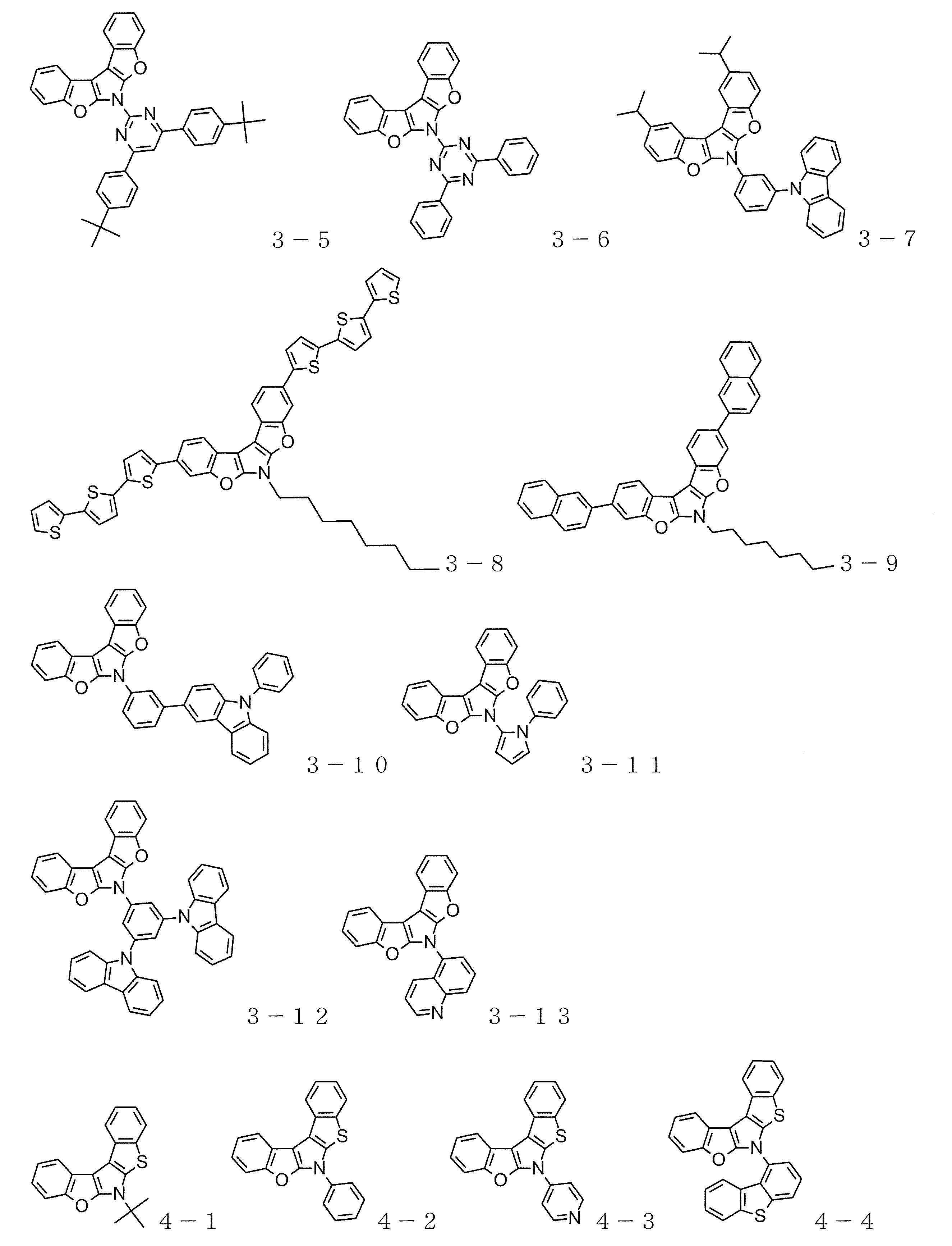


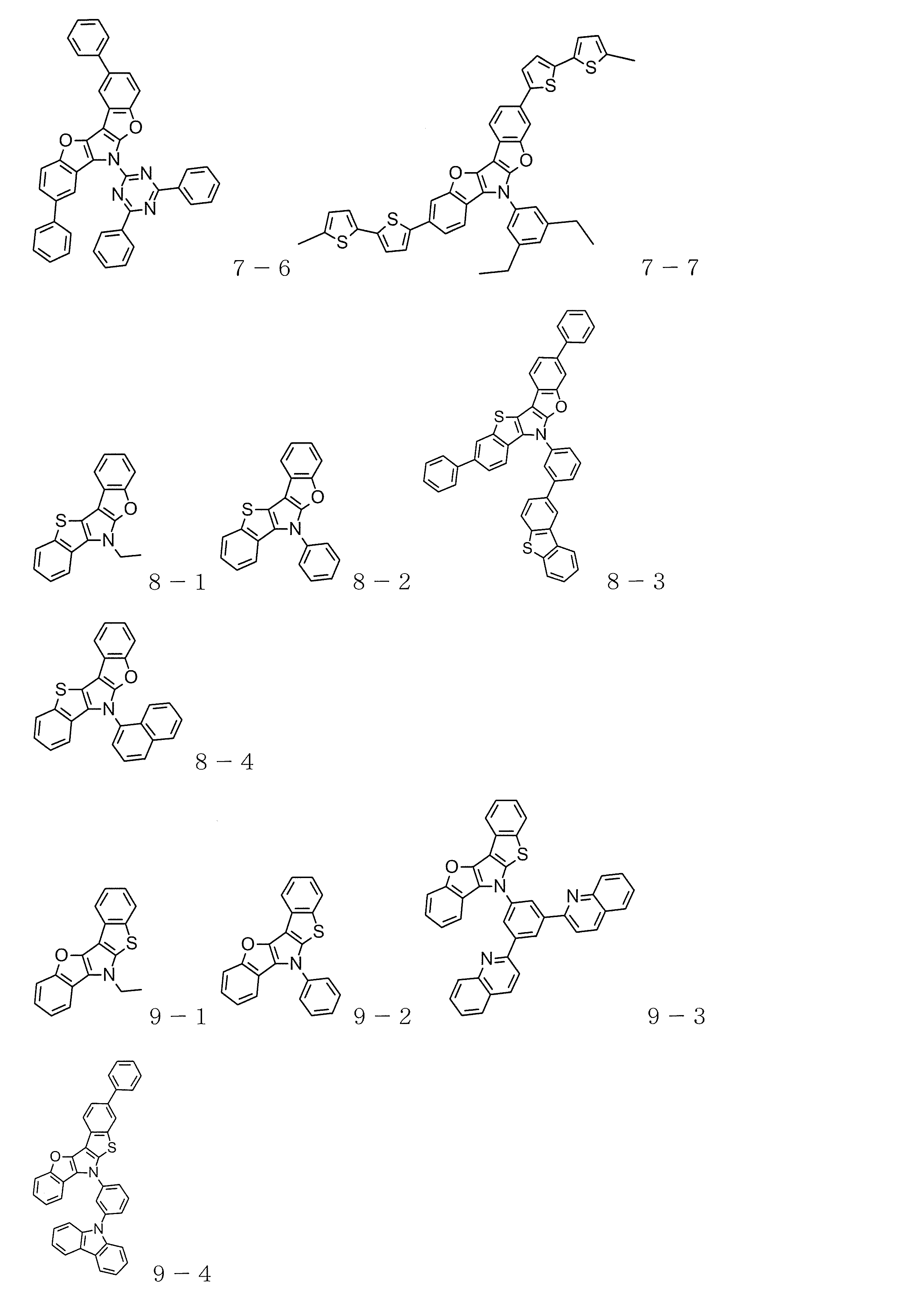


次に、本発明の有機半導体材料および本発明の有機電子デバイスについて説明する。本発明の有機半導体材料は、式(1)で表されるヘテロアセン化合物(本発明のヘテロアセン化合物ともいう。)を含む有機半導体材料である。本発明の有機半導体材料は、本発明のヘテロアセン化合物を含むものであればよく、例えば、他の有機半導体材料に混合して用いてもよく、また、種々のドーパントを含んでいてもよい。ドーパントとしては、例えば、有機EL素子の発光層として用いる場合には、クマリン、キナクリドン、ルブレン、スチルベン系誘導体および蛍光色素、イリジウム錯体や白金錯体等の貴金属錯体を用いることができる。
本発明の有機電子デバイスは、本発明の有機半導体材料を用いた有機電子デバイスである。すなわち、本発明の有機電子デバイスは、本発明のヘテロアセン化合物を含む有機電子デバイスである。具体的には、本発明の有機電子デバイスは、少なくとも1層の有機層を備え、この有機層のうち少なくとも1層が上述した本発明の化合物を含む。
本発明の有機電子デバイスは、種々の態様とすることができるが、好適態様の一つとして、有機EL素子が挙げられる。具体的には、基板上に、陽極、発光層を含む有機層及び陰極が積層されてなる有機EL素子からなる有機電子デバイスであって、前記有機層が上述した本発明のヘテロアセン化合物を含む有機電子デバイスである。
本発明の有機EL素子の構造について、図面を参照しながら説明するが、本発明の有機EL素子の構造は何ら図示のものに限定されるものではない。
図1は本発明に用いられる一般的な有機EL素子の構造例を示す断面図であり、1は基板、2は陽極、3は正孔注入層、4は正孔輸送層、5は発光層、6は電子輸送層、7は陰極を各々表わす。本発明の有機EL素子では発光層と隣接して励起子阻止層を有してもよく、また、発光層と正孔注入層との間に電子阻止層を有しても良い。励起子阻止層は発光層の陽極側、陰極側のいずれにも挿入することができ、両方同時に挿入することも可能である。本発明の有機EL素子では、基板、陽極、発光層及び陰極を必須の層として有するが、必須の層以外の層に、正孔注入輸送層、電子注入輸送層を有することがよく、更に発光層と電子注入輸送層の間に正孔阻止層を有することがよい。なお、正孔注入輸送層は、正孔注入層と正孔輸送層のいずれか又は両者を意味し、電子注入輸送層は、電子注入層と電子輸送層のいずれか又は両者を意味する。
なお、図1とは逆の構造、すなわち、基板1上に陰極7、電子輸送層6、発光層5、正孔輸送層4、陽極2の順に積層することも可能であり、この場合も、必要により層を追加したり、省略したりすることが可能である。
本発明のヘテロアセン化合物は有機EL素子中のいずれの層にも使用できる。発光層、正孔輸送層、電子阻止層、正孔阻止層、電子輸送層で使用することが好ましく、発光層、正孔輸送層、電子阻止層として使用することが特に好ましい。
-基板-
本発明の有機EL素子は、基板に支持されていることが好ましい。この基板については、特に制限はなく、従来から有機EL素子に慣用されているものであればよく、例えば、ガラス、透明プラスチック、石英などからなるものを用いることができる。
本発明の有機EL素子は、基板に支持されていることが好ましい。この基板については、特に制限はなく、従来から有機EL素子に慣用されているものであればよく、例えば、ガラス、透明プラスチック、石英などからなるものを用いることができる。
-陽極-
有機EL素子における陽極としては、仕事関数の大きい(4eV以上)金属、合金、電気伝導性化合物及びこれらの混合物を電極物質とするものが好ましく用いられる。このような電極物質の具体例としてはAu等の金属、CuI、インジウムチンオキシド(ITO)、SnO2、ZnO等の導電性透明材料が挙げられる。また、IDIXO(In2O3-ZnO)等非晶質で透明導電膜を作製可能な材料を用いてもよい。陽極はこれらの電極物質を蒸着やスパッタリング等の方法により、薄膜を形成させ、フォトリソグラフィー法で所望の形状のパターンを形成してもよく、あるいはパターン精度をあまり必要としない場合は(100μm以上程度)、上記電極物質の蒸着やスパッタリング時に所望の形状のマスクを介してパターンを形成してもよい。あるいは、有機導電性化合物のように塗布可能な物質を用いる場合には、印刷方式、コーティング方式等湿式成膜法を用いることもできる。この陽極より発光を取り出す場合には、透過率を10%より大きくすることが望ましく、また陽極としてのシート抵抗は数百Ω/□以下が好ましい。更に膜厚は材料にもよるが、通常10~1000nm、好ましくは10~200nmの範囲で選ばれる。
有機EL素子における陽極としては、仕事関数の大きい(4eV以上)金属、合金、電気伝導性化合物及びこれらの混合物を電極物質とするものが好ましく用いられる。このような電極物質の具体例としてはAu等の金属、CuI、インジウムチンオキシド(ITO)、SnO2、ZnO等の導電性透明材料が挙げられる。また、IDIXO(In2O3-ZnO)等非晶質で透明導電膜を作製可能な材料を用いてもよい。陽極はこれらの電極物質を蒸着やスパッタリング等の方法により、薄膜を形成させ、フォトリソグラフィー法で所望の形状のパターンを形成してもよく、あるいはパターン精度をあまり必要としない場合は(100μm以上程度)、上記電極物質の蒸着やスパッタリング時に所望の形状のマスクを介してパターンを形成してもよい。あるいは、有機導電性化合物のように塗布可能な物質を用いる場合には、印刷方式、コーティング方式等湿式成膜法を用いることもできる。この陽極より発光を取り出す場合には、透過率を10%より大きくすることが望ましく、また陽極としてのシート抵抗は数百Ω/□以下が好ましい。更に膜厚は材料にもよるが、通常10~1000nm、好ましくは10~200nmの範囲で選ばれる。
-陰極-
一方、陰極としては、仕事関数の小さい(4eV以下)金属(電子注入性金属と称する)、合金、電気伝導性化合物及びこれらの混合物を電極物質とするものが用いられる。このような電極物質の具体例としては、ナトリウム、ナトリウム-カリウム合金、マグネシウム、リチウム、マグネシウム/銅混合物、マグネシウム/銀混合物、マグネシウム/アルミニウム混合物、マグネシウム/インジウム混合物、アルミニウム/酸化アルミニウム(Al2O3)混合物、インジウム、リチウム/アルミニウム混合物、希土類金属等が挙げられる。これらの中で、電子注入性及び酸化等に対する耐久性の点から、電子注入性金属とこれより仕事関数の値が大きく安定な金属である第二金属との混合物、例えば、マグネシウム/銀混合物、マグネシウム/アルミニウム混合物、マグネシウム/インジウム混合物、アルミニウム/酸化アルミニウム(Al2O3)混合物、リチウム/アルミニウム混合物、アルミニウム等が好適である。陰極はこれらの電極物質を蒸着やスパッタリング等の方法により薄膜を形成させることにより、作製することができる。また、陰極としてのシート抵抗は数百Ω/□以下が好ましく、膜厚は通常10nm~5μm、好ましくは50~200nmの範囲で選ばれる。なお、発光した光を透過させるため、有機EL素子の陽極又は陰極のいずれか一方が、透明又は半透明であれば発光輝度が向上し好都合である。
一方、陰極としては、仕事関数の小さい(4eV以下)金属(電子注入性金属と称する)、合金、電気伝導性化合物及びこれらの混合物を電極物質とするものが用いられる。このような電極物質の具体例としては、ナトリウム、ナトリウム-カリウム合金、マグネシウム、リチウム、マグネシウム/銅混合物、マグネシウム/銀混合物、マグネシウム/アルミニウム混合物、マグネシウム/インジウム混合物、アルミニウム/酸化アルミニウム(Al2O3)混合物、インジウム、リチウム/アルミニウム混合物、希土類金属等が挙げられる。これらの中で、電子注入性及び酸化等に対する耐久性の点から、電子注入性金属とこれより仕事関数の値が大きく安定な金属である第二金属との混合物、例えば、マグネシウム/銀混合物、マグネシウム/アルミニウム混合物、マグネシウム/インジウム混合物、アルミニウム/酸化アルミニウム(Al2O3)混合物、リチウム/アルミニウム混合物、アルミニウム等が好適である。陰極はこれらの電極物質を蒸着やスパッタリング等の方法により薄膜を形成させることにより、作製することができる。また、陰極としてのシート抵抗は数百Ω/□以下が好ましく、膜厚は通常10nm~5μm、好ましくは50~200nmの範囲で選ばれる。なお、発光した光を透過させるため、有機EL素子の陽極又は陰極のいずれか一方が、透明又は半透明であれば発光輝度が向上し好都合である。
また、陰極に上記金属を1~20nmの膜厚で作製した後に、陽極の説明で挙げた導電性透明材料をその上に作製することで、透明又は半透明の陰極を作製することができ、これを応用することで陽極と陰極の両方が透過性を有する素子を作製することができる。
-発光層-
発光層は蛍光発光層、燐光発光層のいずれでも良いが、燐光発光層であることが好ましい。
発光層は蛍光発光層、燐光発光層のいずれでも良いが、燐光発光層であることが好ましい。
発光層が蛍光発光層である場合、蛍光発光材料は少なくとも1種の蛍光発光材料を単独で使用しても構わないが、蛍光発光材料を蛍光発光ドーパントとして使用し、ホスト材料を含むことが好ましい。
発光層における蛍光発光材料としては、一般式(1)で表されるヘテロアセン化合物化合物を用いることができるが、該化合物を他の何れかの有機層に使用する場合は、多数の特許文献等により知られているので、それらから選択することもできる。例えばベンゾオキサゾール誘導体、ベンゾイミダゾール誘導体、ベンゾチアゾール誘導体、スチリルベンゼン誘導体、ポリフェニル誘導体、ジフェニルブタジエン誘導体、テトラフェニルブタジエン誘導体、ナフタルイミド誘導体、クマリン誘導体、縮合芳香族化合物、ペリノン誘導体、オキサジアゾール誘導体、オキサジン誘導体、アルダジン誘導体、ピラリジン誘導体、シクロペンタジエン誘導体、ビススチリルアントラセン誘導体、キナクリドン誘導体、ピロロピリジン誘導体、チアジアゾロピリジン誘導体、シクロペンタジエン誘導体、スチリルアミン誘導体、ジケトピロロピロール誘導体、芳香族ジメチリジン化合物、8-キノリノール誘導体の金属錯体やピロメテン誘導体の金属錯体、希土類錯体、遷移金属錯体に代表される各種金属錯体等、ポリチオフェン、ポリフェニレン、ポリフェニレンビニレン等のポリマー化合物、有機シラン誘導体等が挙げられる。好ましくは縮合芳香族化合物、スチリル化合物、ジケトピロロピロール化合物、オキサジン化合物、ピロメテン金属錯体、遷移金属錯体、ランタノイド錯体が挙げられ、より好ましくは、ナフタセン、ピレン、クリセン、トリフェニレン、ベンゾ[c]フェナントレン、ベンゾ[a]アントラセン、ベンタセン、ペリレン、フルオランテン、アセナフソフルオランテン、ジベンゾ[a,j]アントラセン、ジベンゾ[a,h]アントラセン、ベンゾ[a]ナフタセン、ヘキサセン、アンタントレン、ナフト[2,1‐f]イソキノリン、α-ナフタフェナントリジン、フェナントロオキサゾール、キノリノ[6,5‐f]キノリン、ベンゾチオファントレンなどが挙げられる。これらは置換基としてアリール基、ヘテロアリール基、ジアリールアミノ基、アルキル基を有していてもよい。
前記蛍光発光材料を蛍光発光ドーパントとして使用し、ホスト材料を含む場合、蛍光発光ドーパントが発光層中に含有される量は、0.01~20重量%、好ましくは0.1~10重量%の範囲にあることがよい。
通常、有機EL素子は、陽極、陰極の両電極より発光物質に電荷を注入し、励起状態の発光物質を生成し、発光させる。電荷注入型の有機EL素子の場合、生成した励起子のうち、励起一重項状態に励起されるのは25%であり、残り75%は励起三重項状態に励起されると言われている。第57回応用物理学関係連合講演会 講演予稿集(19p-ZK-4及び19p-ZK-5)に示されているように、特定の蛍光発光物質は、系間交差等により励起三重項状態へとエネルギーが遷移した後、三重項-三重項消滅あるいは熱エネルギーの吸収により、励起一重項状態に逆系間交差され蛍光を放射し、熱活性遅延蛍光を発現することが知られている。本発明の化合物を用いた有機EL素子でも遅延蛍光を発現することができる。この場合、蛍光発光及び遅延蛍光発光の両方を含むこともできる。但し、発光の一部或いは部分的にホスト材料からの発光があっても良い。
発光層が燐光発光層である場合、燐光発光ドーパントとホスト材料を含む。燐光発光ドーパント材料としては、ルテニウム、ロジウム、パラジウム、銀、レニウム、オスミウム、イリジウム、白金及び金から選ばれる少なくとも一つの金属を含む有機金属錯体を含有するものがよい。かかる有機金属錯体は、前記先行技術文献等で公知であり、これらが選択されて使用可能である。
好ましい燐光発光ドーパントとしては、Ir等の貴金属元素を中心金属として有するIr(ppy)3等の錯体類、(Bt)2Iracac等の錯体類、(Btp)Ptacac等の錯体類が挙げられる。これらの錯体類の具体例を以下に示すが、下記の化合物に限定されない。
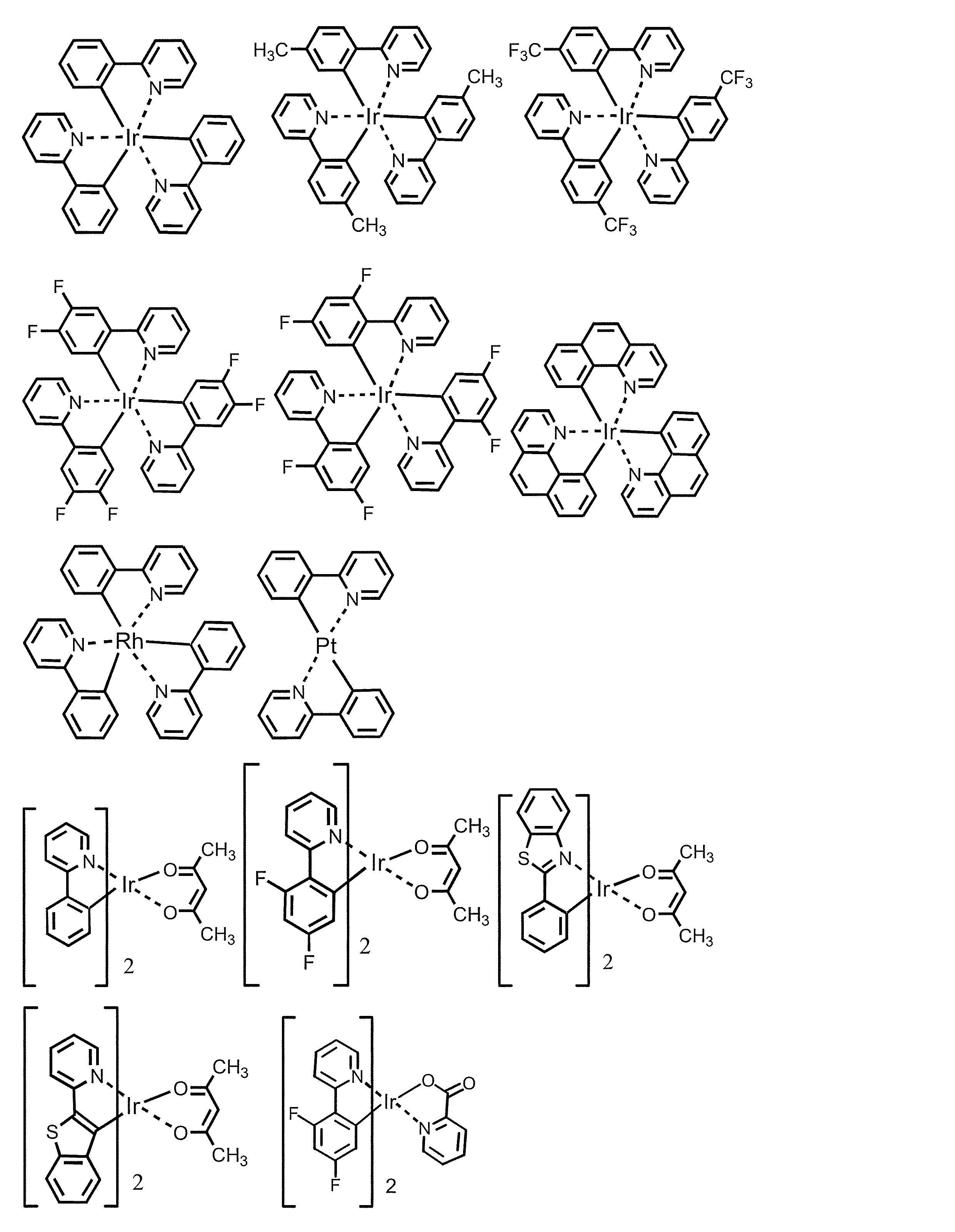

前記燐光発光ドーパントが発光層中に含有される量は、1~50重量%の範囲にあることが好ましい。より好ましくは5~30重量%である。
発光層におけるホスト材料としては、前記一般式(1)で表される本発明のヘテロアセン化合物を用いることが好ましい。しかし、該化合物を発光層以外の他の何れかの有機層に使用する場合は、発光層に使用する材料は本発明の化合物以外の他のホスト材料であってもよい。また、本発明のヘテロアセン化合物と他のホスト材料を併用してもよい。更に、公知のホスト材料を複数種類併用して用いてもよい。
使用できる公知のホスト化合物としては、正孔輸送能又は電子輸送能を有し、かつ発光の長波長化を防ぎ、なおかつ高いガラス転移温度を有する化合物であることが好ましい。
このような他のホスト材料は、多数の特許文献等により知られているので、それらから選択することができる。ホスト材料の具体例としては、特に限定されるものではないが、インドール誘導体、カルバゾール誘導体、インドロカルバゾール誘導体、トリアゾール誘導体、オキサゾール誘導体、オキサジアゾール誘導体、イミダゾール誘導体、ポリアリールアルカン誘導体、ピラゾリン誘導体、ピラゾロン誘導体、フェニレンジアミン誘導体、アリールアミン誘導体、アミノ置換カルコン誘導体、スチリルアントラセン誘導体、フルオレノン誘導体、ヒドラゾン誘導体、スチルベン誘導体、シラザン誘導体、芳香族第三アミン化合物、スチリルアミン化合物、芳香族ジメチリデン系化合物、ポルフィリン系化合物、アントラキノジメタン誘導体、アントロン誘導体、ジフェニルキノン誘導体、チオピランジオキシド誘導体、ナフタレンペリレン等の複素環テトラカルボン酸無水物、フタロシアニン誘導体、8‐キノリノール誘導体の金属錯体やメタルフタロシアニン、ベンゾオキサゾールやベンゾチアゾール誘導体の金属錯体に代表される各種金属錯体、ポリシラン系化合物、ポリ(N-ビニルカルバゾール)誘導体、アニリン系共重合体、チオフェンオリゴマー、ポリチオフェン誘導体、ポリフェニレン誘導体、ポリフェニレンビニレン誘導体、ポリフルオレン誘導体等の高分子化合物等が挙げられる。
-注入層-
注入層とは、駆動電圧低下や発光輝度向上のために電極と有機層間に設けられる層のことで、正孔注入層と電子注入層があり、陽極と発光層又は正孔輸送層の間、及び陰極と発光層又は電子輸送層との間に存在させてもよい。注入層は必要に応じて設けることができる。注入材料としては、本発明のヘテロアセン化合物を用いることができるが、該化合物を他の何れかの有機層に使用する場合は、従来公知の化合物の中から任意のものを選択して用いることができる。
注入層とは、駆動電圧低下や発光輝度向上のために電極と有機層間に設けられる層のことで、正孔注入層と電子注入層があり、陽極と発光層又は正孔輸送層の間、及び陰極と発光層又は電子輸送層との間に存在させてもよい。注入層は必要に応じて設けることができる。注入材料としては、本発明のヘテロアセン化合物を用いることができるが、該化合物を他の何れかの有機層に使用する場合は、従来公知の化合物の中から任意のものを選択して用いることができる。
-正孔阻止層-
正孔阻止層とは広い意味では電子輸送層の機能を有し、電子を輸送する機能を有しつつ正孔を輸送する能力が著しく小さい正孔阻止材料からなり、電子を輸送しつつ正孔を阻止することで電子と正孔の再結合確率を向上させることができる。
正孔阻止層とは広い意味では電子輸送層の機能を有し、電子を輸送する機能を有しつつ正孔を輸送する能力が著しく小さい正孔阻止材料からなり、電子を輸送しつつ正孔を阻止することで電子と正孔の再結合確率を向上させることができる。
正孔阻止層には本発明のヘテロアセン化合物を用いることが好ましいが、該化合物を他の何れかの有機層に使用する場合は、公知の正孔阻止層材料を用いてもよい。また、正孔阻止層材料としては、後述する電子輸送層の材料を必要に応じて用いることができる。
-電子阻止層-
電子阻止層とは、正孔を輸送する機能を有しつつ電子を輸送する能力が著しく小さい材料から成り、正孔を輸送しつつ電子を阻止することで電子と正孔が再結合する確率を向上させることができる。
電子阻止層とは、正孔を輸送する機能を有しつつ電子を輸送する能力が著しく小さい材料から成り、正孔を輸送しつつ電子を阻止することで電子と正孔が再結合する確率を向上させることができる。
電子阻止層の材料としては、一般式(1)で表される本発明のヘテロアセン化合物を用いることができるが、該化合物を他の何れかの有機層に使用する場合は、後述する正孔輸送層の材料を必要に応じて用いることができる。電子阻止層の膜厚は好ましくは3~100nmであり、より好ましくは5~30nmである。
-励起子阻止層-
励起子阻止層とは、発光層内で正孔と電子が再結合することにより生じた励起子が電荷輸送層に拡散することを阻止するための層であり、本層の挿入により励起子を効率的に発光層内に閉じ込めることが可能となり、素子の発光効率を向上させることができる。励起子阻止層は発光層に隣接して陽極側、陰極側のいずれにも挿入することができ、両方同時に挿入することも可能である。
励起子阻止層とは、発光層内で正孔と電子が再結合することにより生じた励起子が電荷輸送層に拡散することを阻止するための層であり、本層の挿入により励起子を効率的に発光層内に閉じ込めることが可能となり、素子の発光効率を向上させることができる。励起子阻止層は発光層に隣接して陽極側、陰極側のいずれにも挿入することができ、両方同時に挿入することも可能である。
励起子阻止層の材料としては、本発明のヘテロアセン化合物を用いることができるが、該化合物を他の何れかの有機層に使用する場合は、従来公知の化合物の中から任意のものを選択して用いることができる。例えば、1,3-ジカルバゾリルベンゼン(mCP)や、ビス(2-メチル-8-キノリノラト)-4-フェニルフェノラトアルミニウム(III)(BAlq)が挙げられる。
-正孔輸送層-
正孔輸送層とは正孔を輸送する機能を有する正孔輸送材料からなり、正孔輸送層は単層又は複数層設けることができる。
正孔輸送層とは正孔を輸送する機能を有する正孔輸送材料からなり、正孔輸送層は単層又は複数層設けることができる。
正孔輸送材料としては、正孔の注入又は輸送、電子の障壁性のいずれかを有するものであり、有機物、無機物のいずれであってもよい。正孔輸送層には本発明のヘテロアセン化合物を用いることが好ましいが、該化合物を他の何れかの有機層に使用する場合は、従来公知の化合物の中から任意のものを選択して用いることができる。使用できる公知の正孔輸送材料としては例えば、トリアゾール誘導体、オキサジアゾール誘導体、イミダゾール誘導体、ポリアリールアルカン誘導体、ピラゾリン誘導体及びピラゾロン誘導体、フェニレンジアミン誘導体、アリールアミン誘導体、アミノ置換カルコン誘導体、オキサゾール誘導体、スチリルアントラセン誘導体、フルオレノン誘導体、ヒドラゾン誘導体、スチルベン誘導体、シラザン誘導体、アニリン系共重合体、また導電性高分子オリゴマー、特にチオフェンオリゴマー等が挙げられるが、ポルフィリン化合物、芳香族第3級アミン化合物及びスチリルアミン化合物を用いることが好ましく、芳香族第3級アミン化合物を用いることがより好ましい。
-電子輸送層-
電子輸送層とは電子を輸送する機能を有する材料からなり、電子輸送層は単層又は複数層設けることができる。
電子輸送層とは電子を輸送する機能を有する材料からなり、電子輸送層は単層又は複数層設けることができる。
電子輸送材料(正孔阻止材料を兼ねる場合もある)としては、陰極より注入された電子を発光層に伝達する機能を有していればよい。電子輸送層には本発明のヘテロアセン化合物を用いることが好ましいが、該化合物を他の何れかの有機層に使用する場合は、従来公知の化合物の中から任意のものを選択して用いることができ、例えば、ニトロ置換フルオレン誘導体、ジフェニルキノン誘導体、チオピランジオキシド誘導体、カルボジイミド、フレオレニリデンメタン誘導体、アントラキノジメタン及びアントロン誘導体、オキサジアゾール誘導体等が挙げられる。更に、上記オキサジアゾール誘導体において、オキサジアゾール環の酸素原子を硫黄原子に置換したチアジアゾール誘導体、電子吸引基として知られているキノキサリン環を有するキノキサリン誘導体も、電子輸送材料として用いることができる。更にこれらの材料を高分子鎖に導入した、又はこれらの材料を高分子の主鎖とした高分子材料を用いることもできる。
本発明の化合物を含む有機電子デバイスの別の好適態様の一つとして、有機TFT素子が挙げられる。具体的には、基板上に、ゲート電極と、ゲート絶縁層と、有機半導体層と、ソース電極およびドレイン電極とを有する有機TFT素子からなる有機電子デバイスであって、前記有機半導体層が上述した本発明のヘテロアセン化合物を含む有機電子デバイスである。
本発明の有機TFT素子の構造について、図面を参照しながら説明するが、本発明の有機TFT素子の構造は何ら図示のものに限定されるものではない。
図2及び図3は一般的な本発明の有機TFT素子の構造例を示す断面図であり、8は基板、9はゲート電極、10は絶縁層、11は有機半導体層、12はソース電極、13はドレイン電極を各々表わす。
-基板-
基板は、特に限定されず、例えば、従来公知の構成とすることができる。基板としては、例えば、ガラス(例えば、石英ガラス)、シリコン、セラミック、プラスチックが挙げられる。プラスチックとしては、例えば、ポリエチレンテレフタレート、ポリエチレンナフタレート、ポリカーボネート等の汎用の樹脂基板が挙げられる。樹脂基板は、酸素、水蒸気等のガスの透過性を低くするためのガスバリア膜を積層したものであることが好ましい。
基板は、特に限定されず、例えば、従来公知の構成とすることができる。基板としては、例えば、ガラス(例えば、石英ガラス)、シリコン、セラミック、プラスチックが挙げられる。プラスチックとしては、例えば、ポリエチレンテレフタレート、ポリエチレンナフタレート、ポリカーボネート等の汎用の樹脂基板が挙げられる。樹脂基板は、酸素、水蒸気等のガスの透過性を低くするためのガスバリア膜を積層したものであることが好ましい。
-ゲート電極-
ゲート電極は、特に限定されず、例えば、従来公知の構成とすることができる。ゲート電極としては、例えば、金、白金、クロム、タングステン、タンタル、ニッケル、銅、アルミニウム、銀、マグネシウム、カルシウム等の金属またはそれらの合金、ポリシリコン、アモルファスシリコン、グラファイト、ITO、酸化亜鉛、導電性ポリマー等の材料を用いることができる。
ゲート電極は、特に限定されず、例えば、従来公知の構成とすることができる。ゲート電極としては、例えば、金、白金、クロム、タングステン、タンタル、ニッケル、銅、アルミニウム、銀、マグネシウム、カルシウム等の金属またはそれらの合金、ポリシリコン、アモルファスシリコン、グラファイト、ITO、酸化亜鉛、導電性ポリマー等の材料を用いることができる。
-ゲート絶縁層-
ゲート絶縁層は、特に限定されず、例えば、従来公知の構成とすることができる。ゲート絶縁層としては、SiO2、Si3N4、SiON、Al2O3、Ta2O5、アモルファスシリコン、ポリイミド樹脂、ポリビニルフェノール樹脂、ポリパラキシリレン樹脂、ポリメチルメタクリレート樹脂、フッ素樹脂(PTFE、PFA、PETFE、PCTFE、CYTOP(登録商標)等)等の材料を用いることができる。
ゲート絶縁層は、特に限定されず、例えば、従来公知の構成とすることができる。ゲート絶縁層としては、SiO2、Si3N4、SiON、Al2O3、Ta2O5、アモルファスシリコン、ポリイミド樹脂、ポリビニルフェノール樹脂、ポリパラキシリレン樹脂、ポリメチルメタクリレート樹脂、フッ素樹脂(PTFE、PFA、PETFE、PCTFE、CYTOP(登録商標)等)等の材料を用いることができる。
-有機半導体層-
有機半導体層は、本発明のヘテロアセン化合物を含む層であれば、特に限定されない。例えば、実質的に本発明のヘテロアセン化合物のみからなる層であってもよく、他の物質を含有する層であってもよい。
有機半導体層は、本発明のヘテロアセン化合物を含む層であれば、特に限定されない。例えば、実質的に本発明のヘテロアセン化合物のみからなる層であってもよく、他の物質を含有する層であってもよい。
-ソース電極およびドレイン電極-
ソース電極およびドレイン電極は、いずれも特に限定されず、例えば、従来公知の構成とすることができる。ソース電極およびドレイン電極としては、いずれも、金、白金、クロム、タングステン、タンタル、ニッケル、銅、アルミニウム、銀、マグネシウム、カルシウム等の金属またはそれらの合金、ポリシリコン、アモルファスシリコン、グラファイト、ITO、酸化亜鉛、導電性ポリマー等の材料を用いることができる。
ソース電極およびドレイン電極は、いずれも特に限定されず、例えば、従来公知の構成とすることができる。ソース電極およびドレイン電極としては、いずれも、金、白金、クロム、タングステン、タンタル、ニッケル、銅、アルミニウム、銀、マグネシウム、カルシウム等の金属またはそれらの合金、ポリシリコン、アモルファスシリコン、グラファイト、ITO、酸化亜鉛、導電性ポリマー等の材料を用いることができる。
有機TFT素子における積層の構成は、基板側から、ゲート電極と、ゲート絶縁層と、有機半導体層と、ソース電極およびドレイン電極とをこの順に有する構成(i)、および、基板側から、ゲート電極と、ゲート絶縁層と、ソース電極およびドレイン電極と、有機半導体層とをこの順に有する構成(ii)のいずれであってもよい。有機TFT素子の作製方法は、特に限定されないが、構成(i)の場合、例えば、基板上に、ゲート電極と、ゲート絶縁層と、有機半導体層と、ドレイン電極およびソース電極とを順次積層するトップコンタクト法が挙げられ、構成(ii)の場合、基板上に、ゲート電極と、ゲート絶縁層と、ドレイン電極およびソース電極と、有機半導体層とを順次積層するボトムコンタクト法が挙げられる。
ゲート電極と、ゲート絶縁層と、ソース電極およびドレイン電極とは、形成方法を特に限定されないが、いずれも、例えば、上述した材料を用いて、真空蒸着法、電子ビーム蒸着法、RFスパッタ法、スピンコート法、印刷法等の周知の膜作製方法により形成させることができる。有機半導体層は、形成方法を特に限定されないが、例えば、本発明のヘテロアセン化合物又は有機半導体材料を用いて、真空蒸着法、スピンコート法、インクジェット法、印刷法等の周知の膜作製方法により形成させることができる。
有機TFT素子は、用途を特に限定されないが、例えばプラスチック基板を用いたフレキシブルディスプレイの駆動用TFT素子として好適に用いられる。一般的にプラスチック基板上に無機物で構成されたTFT素子を作製することはプロセス上困難である。しかし、有機TFT素子からなる本発明の有機電子デバイスの作製工程では、上述したように真空蒸着法、スピンコート法、インクジェット法、印刷法等のプロセスを用い、高温プロセスを使用しないため、プラスチック基板上に画素駆動用のTFT素子を形成しうる。特に、本発明のヘテロアセン化合物は、クロロホルム、テトラヒドロフラン、トルエン等の汎用有機溶媒に可溶であるため、スピンコート法、インクジェット法、印刷法等の低コストプロセスを適用可能であり、安価なペーパーライク(フレキシブル)ディスプレイの作製に適している。
本発明のヘテロアセン化合物を含む有機電子デバイスの別の好適態様の一つとして、光起電力素子が挙げられる。具体的には、基板上に、正極、有機半導体層及び負極を有する光起電力素子であって、前記有機半導体層が上述した本発明のヘテロアセン化合物を含む有機電子デバイスである。
本発明の光起電力素子の構造について、図面を参照しながら説明するが、本発明の光起電力素子の構造は何ら図示のものに限定されるものではない。
図4は一般的な本発明の光起電力素子の構造例を示す断面図であり、14は基板、15は正極、16は有機半導体層、17は負極を各々表わす。また、図5は有機半導体層が積層されている場合の構造例を示す断面図であり、16-aは電子供与性有機半導体層、16-bは電子受容性有機半導体層である。
-基板-
基板は、特に限定されず、例えば、従来公知の構成とすることができる。機械的、熱的強度を有し、透明性を有するガラス基板や透明性樹脂フィルムを使用することが好ましい。透明性樹脂フィルムとしては、ポリエチレン、エチレン-酢酸ビニル共重合体、エチレン-ビニルアルコール共重合体、ポリプロピレン、ポリスチレン、ポリメチルメタアクリレート、ポリ塩化ビニル、ポリビニルアルコール、ポリビニルブチラール、ナイロン、ポリエーテルエーテルケトン、ポリサルホン、ポリエーテルサルフォン、テトラフルオロエチレン-パーフルオロアルキルビニルエーテル共重合体、ポリビニルフルオライド、テトラフルオロエチレン-エチレン共重合体、テトラフルオロエチレン-ヘキサフルオロプロピレン共重合体、ポリクロロトリフルオロエチレン、ポリビニリデンフルオライド、ポリエステル、ポリカーボネート、ポリウレタン、ポリイミド、ポリエーテルイミド、ポリイミド、ポリプロピレン等が挙げられる。
基板は、特に限定されず、例えば、従来公知の構成とすることができる。機械的、熱的強度を有し、透明性を有するガラス基板や透明性樹脂フィルムを使用することが好ましい。透明性樹脂フィルムとしては、ポリエチレン、エチレン-酢酸ビニル共重合体、エチレン-ビニルアルコール共重合体、ポリプロピレン、ポリスチレン、ポリメチルメタアクリレート、ポリ塩化ビニル、ポリビニルアルコール、ポリビニルブチラール、ナイロン、ポリエーテルエーテルケトン、ポリサルホン、ポリエーテルサルフォン、テトラフルオロエチレン-パーフルオロアルキルビニルエーテル共重合体、ポリビニルフルオライド、テトラフルオロエチレン-エチレン共重合体、テトラフルオロエチレン-ヘキサフルオロプロピレン共重合体、ポリクロロトリフルオロエチレン、ポリビニリデンフルオライド、ポリエステル、ポリカーボネート、ポリウレタン、ポリイミド、ポリエーテルイミド、ポリイミド、ポリプロピレン等が挙げられる。
-電極-
電極材料としては、一方の電極には仕事関数の大きな導電性素材、もう一方の電極には仕事関数の小さな導電性素材を使用することが好ましい。仕事関数の大きな導電性素材を用いた電極は正極となる。この仕事関数の大きな導電性素材としては金、白金、クロム、ニッケルなどの金属のほか、透明性を有するインジウム、スズなどの金属酸化物、複合金属酸化物(インジウム錫酸化物(ITO)、インジウム亜鉛酸化物(IZO)など)が好ましく用いられる。ここで、正極に用いられる導電性素材は、有機半導体層とオーミック接合するものであることが好ましい。さらに、後述する正孔輸送層を用いた場合においては、正極に用いられる導電性素材は正孔輸送層とオーミック接合するものであることが好ましい。
電極材料としては、一方の電極には仕事関数の大きな導電性素材、もう一方の電極には仕事関数の小さな導電性素材を使用することが好ましい。仕事関数の大きな導電性素材を用いた電極は正極となる。この仕事関数の大きな導電性素材としては金、白金、クロム、ニッケルなどの金属のほか、透明性を有するインジウム、スズなどの金属酸化物、複合金属酸化物(インジウム錫酸化物(ITO)、インジウム亜鉛酸化物(IZO)など)が好ましく用いられる。ここで、正極に用いられる導電性素材は、有機半導体層とオーミック接合するものであることが好ましい。さらに、後述する正孔輸送層を用いた場合においては、正極に用いられる導電性素材は正孔輸送層とオーミック接合するものであることが好ましい。
仕事関数の小さな導電性素材を用いた電極は負極となるが、この仕事関数の小さな導電性素材としては、アルカリ金属やアルカリ土類金属、具体的にはリチウム、マグネシウム、カルシウムが使用される。また、錫や銀、アルミニウムも好ましく用いられる。さらに、上記の金属からなる合金や上記の金属の積層体からなる電極も好ましく用いられる。また、負極と電子輸送層の界面にフッ化リチウムやフッ化セシウムなどの金属フッ化物を導入することで、取り出し電流を向上させることも可能である。ここで、負極に用いられる導電性素材は、有機半導体層とオーミック接合するものであることが好ましい。さらに、後述する電子輸送層を用いた場合においては、負極に用いられる導電性素材は電子輸送層とオーミック接合するものであることが好ましい。
-有機半導体層-
有機半導体層は本発明のヘテロアセン化合物を含む。すなわち、一般式(1)で表されるヘテロアセン化合物を含む電子供与性有機材料および電子受容性有機材料を含む。これらの材料は混合されていることが好ましく、電子供与性有機材料と電子受容性有機材料が分子レベルで相溶しているか、相分離していることが好ましい。この相分離構造のドメインサイズは特に限定されるものではないが通常1nm以上50nm以下のサイズである。また、電子供与性有機材料と電子受容性有機材料が積層されている場合は、p型半導体特性を示す電子供与性有機材料を有する層が正極側、n型半導体特性を示す電子受容性有機材料を有する層が負極側であることが好ましい。有機半導体層は5nm~500nmの厚さが好ましく、より好ましくは30nm~300nmである。積層されている場合は、本発明のヘテロアセン化合物を電子供与性有機材料として有する層は上記厚さのうち1nm~400nmの厚さを有していることが好ましく、より好ましくは15nm~150nmである。
有機半導体層は本発明のヘテロアセン化合物を含む。すなわち、一般式(1)で表されるヘテロアセン化合物を含む電子供与性有機材料および電子受容性有機材料を含む。これらの材料は混合されていることが好ましく、電子供与性有機材料と電子受容性有機材料が分子レベルで相溶しているか、相分離していることが好ましい。この相分離構造のドメインサイズは特に限定されるものではないが通常1nm以上50nm以下のサイズである。また、電子供与性有機材料と電子受容性有機材料が積層されている場合は、p型半導体特性を示す電子供与性有機材料を有する層が正極側、n型半導体特性を示す電子受容性有機材料を有する層が負極側であることが好ましい。有機半導体層は5nm~500nmの厚さが好ましく、より好ましくは30nm~300nmである。積層されている場合は、本発明のヘテロアセン化合物を電子供与性有機材料として有する層は上記厚さのうち1nm~400nmの厚さを有していることが好ましく、より好ましくは15nm~150nmである。
電子供与性有機材料は、本発明のヘテロアセン化合物のみからなるものでもよいし、他の電子供与性有機材料を含んでもよい。他の電子供与性有機材料としては、例えばポリチオフェン系重合体、ベンゾチアジアゾール-チオフェン系誘導体、ベンゾチアジアゾール-チオフェン系共重合体、ポリ-p-フェニレンビニレン系重合体、ポリ-p-フェニレン系重合体、ポリフルオレン系重合体、ポリピロール系重合体、ポリアニリン系重合体、ポリアセチレン系重合体、ポリチエニレンビニレン系重合体などの共役系重合体や、H2フタロシアニン(H2Pc)、銅フタロシアニン(CuPc)、亜鉛フタロシアニン(ZnPc)などのフタロシアニン誘導体、ポルフィリン誘導体、N,N’-ジフェニル-N,N’-ジ(3-メチルフェニル)-4,4’-ジフェニル-1,1’-ジアミン(TPD)、N,N’-ジナフチル-N,N’-ジフェニル-4,4’-ジフェニル-1,1’-ジアミン(NPD)などのトリアリールアミン誘導体、4,4’-ジ(カルバゾール-9-イル)ビフェニル(CBP)などのカルバゾール誘導体、オリゴチオフェン誘導体(ターチオフェン、クウォーターチオフェン、セキシチオフェン、オクチチオフェンなど)などの低分子有機化合物が挙げられる。
上記一般式(1)で表されるヘテロアセン化合物は電子供与性(p型半導体特性)を示すため、本発明の光起電力素子用材料は、さらに電子受容性有機材料(n型有機半導体)を含有することが好ましい。本発明のヘテロアセン化合物と電子受容性有機材料を組み合わせることにより、光起電力素子の光電変換効率をより向上させることができる。
本発明の光起電力素子で用いる電子受容性有機材料とは、n型半導体特性を示す有機材料であり、例えば1,4,5,8-ナフタレンテトラカルボキシリックジアンハイドライド(NTCDA)、3,4,9,10-ペリレンテトラカルボキシリックジアンハイドライド(PTCDA)、3,4,9,10-ペリレンテトラカルボキシリックビスベンズイミダゾール(PTCBI)、N,N'-ジオクチル-3,4,9,10-ナフチルテトラカルボキシジイミド(PTCDI-C8H)、2-(4-ビフェニリル)-5-(4-t-ブチルフェニル)-1,3,4-オキサジアゾール(PBD)、2,5-ジ(1-ナフチル)-1,3,4-オキサジアゾール(BND)などのオキサゾール誘導体、3-(4-ビフェニリル)-4-フェニル-5-(4-t-ブチルフェニル)-1,2,4-トリアゾール(TAZ)などのトリアゾール誘導体、フェナントロリン誘導体、ホスフィンオキサイド誘導体、フラーレン化合物(C60、C70、C76、C78、C82、C84、C90、C94を始めとする無置換のものと、[6,6]-フェニル C61 ブチリックアシッドメチルエステル([6,6]-PCBM)、[5,6]-フェニル C61 ブチリックアシッドメチルエステル([5,6]-PCBM)、[6,6]-フェニル C61 ブチリックアシッドヘキシルエステル([6,6]-PCBH)、[6,6]-フェニル C61 ブチリックアシッドドデシルエステル([6,6]-PCBD)、フェニル C71 ブチリックアシッドメチルエステル(PC70BM)、フェニル C85 ブチリックアシッドメチルエステル(PC84BM)など)、カーボンナノチューブ(CNT)、ポリ-p-フェニレンビニレン系重合体にシアノ基を導入した誘導体(CN-PPV)などが挙げられる。中でも、フラーレン化合物は電荷分離速度と電子移動速度が速いため、好ましく用いられる。
本発明の光起電力素子では、正極と有機半導体層の間に正孔輸送層を設けてもよい。正孔輸送層を形成する材料としては、ポリチオフェン系重合体、ポリ-p-フェニレンビニレン系重合体、ポリフルオレン系重合体などの導電性高分子や、フタロシアニン誘導体(H2Pc、CuPc、ZnPcなど)、ポルフィリン誘導体などのp型半導体特性を示す低分子有機化合物が好ましく用いられる。特に、ポリチオフェン系重合体であるポリエチレンジオキシチオフェン(PEDOT)やPEDOTにポリスチレンスルホネート(PSS)が添加されたものが好ましく用いられる。正孔輸送層は5nm~600nmの厚さが好ましく、より好ましくは30nm~200nmである。
また、本発明の光起電力素子は、有機半導体層と負極の間に電子輸送層を設けてもよい。電子輸送層を形成する材料として、特に限定されるものではないが、上述の電子受容性有機材料(NTCDA、PTCDA、PTCDI-C8H、オキサゾール誘導体、トリアゾール誘導体、フェナントロリン誘導体、ホスフィンオキサイド誘導体、フラーレン化合物、CNT、CN-PPVなど)のようにn型半導体特性を示す有機材料が好ましく用いられる。電子輸送層は5nm~600nmの厚さが好ましく、より好ましくは30nm~200nmである。
また、本発明の光起電力素子は、1つ以上の中間電極を介して2層以上の有機半導体層を積層(タンデム化)して直列接合を形成してもよい。例えば、基板/正極/第1の有機半導体層/中間電極/第2の有機半導体層/負極という積層構成を挙げることができる。このように積層することにより、開放電圧を向上させることができる。なお、正極と第1の有機半導体層の間、および、中間電極と第2の有機半導体層の間に上述の正孔輸送層を設けてもよく、第1の有機半導体層と中間電極の間、および、第2の有機半導体層と負極の間に上述の正孔輸送層を設けてもよい。
このような積層構成の場合、有機半導体層の少なくとも1層が本発明のヘテロアセン化合物を含み、他の層には、短絡電流を低下させないために、本発明の電子供与性有機材料とはバンドギャップの異なる電子供与性有機材料を含むことが好ましい。このような電子供与性有機材料としては、例えば上述のポリチオフェン系重合体、ポリ-p-フェニレンビニレン系重合体、ポリ-p-フェニレン系重合体、ポリフルオレン系重合体、ポリピロール系重合体、ポリアニリン系重合体、ポリアセチレン系重合体、ポリチエニレンビニレン系重合体などの共役系重合体や、H2フタロシアニン(H2Pc)、銅フタロシアニン(CuPc)、亜鉛フタロシアニン(ZnPc)などのフタロシアニン誘導体、ポルフィリン誘導体、N,N’-ジフェニル-N,N’-ジ(3-メチルフェニル)-4,4’-ジフェニル-1,1’-ジアミン(TPD)、N,N’-ジナフチル-N,N’-ジフェニル-4,4’-ジフェニル-1,1’-ジアミン(NPD)などのトリアリールアミン誘導体、4,4’-ジ(カルバゾール-9-イル)ビフェニル(CBP)などのカルバゾール誘導体、オリゴチオフェン誘導体(ターチオフェン、クウォーターチオフェン、セキシチオフェン、オクチチオフェンなど)などの低分子有機化合物が挙げられる。
また、ここで用いられる中間電極用の素材としては高い導電性を有するものが好ましく、例えば上述の金、白金、クロム、ニッケル、リチウム、マグネシウム、カルシウム、錫、銀、アルミニウムなどの金属や、透明性を有するインジウム、スズなどの金属酸化物、複合金属酸化物(インジウム錫酸化物(ITO)、インジウム亜鉛酸化物(IZO)など)、上記の金属からなる合金や上記の金属の積層体、ポリエチレンジオキシチオフェン(PEDOT)やPEDOTにポリスチレンスルホネート(PSS)が添加されたもの、などが挙げられる。中間電極は光透過性を有することが好ましいが、光透過性が低い金属のような素材でも膜厚を薄くすることで充分な光透過性を確保できる場合が多い。
有機半導体層の形成には、スピンコート塗布、ブレードコート塗布、スリットダイコート塗布、スクリーン印刷塗布、バーコーター塗布、鋳型塗布、印刷転写法、浸漬引き上げ法、インクジェット法、スプレー法、真空蒸着法など何れの方法を用いてもよく、膜厚制御や配向制御など、得ようとする有機半導体層特性に応じて形成方法を選択すればよい。
本発明の有機半導体材料は、高電荷移動度、溶媒可溶性、酸化安定性、良好な製膜性を有しており、これを使用した有機半導体デバイスも高い特性を発揮する。本発明の有機半導体材料の特徴を生かせる具体的な有機半導体デバイスとしては、例えば、有機電界効果トランジスタや有機薄膜太陽電池を示すことができ、さらには、これらの有機半導体デバイスを組み込むことにより、有機ELパネルおよび電子ペーパー等のディスプレイ、液晶ディスプレイ、情報タグ、電子人工皮膚シートやシート型スキャナー等の大面積センサーに応用していくことができる。
以下、本発明を実施例によって更に詳しく説明するが、本発明は勿論、これらの実施例に限定されるものではなく、その要旨を越えない限りにおいて、種々の形態で実施することが可能である。
実施例1
化合物1-6の合成
化合物1-6の合成

ベンゾ[b]チオフェン100.0 g(0.75 mol)、クロロホルム300 ml、酢酸300 mlを加え、室温で撹拌した。次にN-ブロモスクシンイミド(NBS)172.4 g(0.97 mol)を加え室温で7時間撹拌した。撹拌終了後、蒸留水600 mlを加え撹拌した。有機層を蒸留水で洗浄し、無水硫酸マグネシウムを用いて乾燥した。硫酸マグネシウムを濾別した後、溶媒を減圧留去した。得られた残渣をシリカゲルカラムクロマトグラフィーによる精製を行なうことでA-1を150.3 g(0.71 mol 収率95%)得た。
マグネシウム2.7 g(0.11 mol)とテトラヒドロフラン(THF) 40mlを加え、70 ℃で30分撹拌した。その後、40 mlのTHFに溶解させたA-1 20.0 g(0.094 mol)を加え、70 ℃で90分撹拌した。その反応溶液を室温まで冷却した後、[1,3-ビス(ジフェニルホスフィノ)プロパン]ニッケル(II)ジクロリド(NiCl2(dppp)) 2.5 g(0.00047 mol)、A-1 20.0 g (0.094 mol)、THF 40mlを加え、70 ℃で3時間撹拌した。反応溶液を室温まで冷却した後、蒸留水200 mlを加えて撹拌した。有機層を蒸留水で洗浄し、無水硫酸マグネシウムを用いて乾燥した。硫酸マグネシウムを濾別した後、溶媒を減圧留去した。得られた残渣をシリカゲルカラムクロマトグラフィーによる精製を行なうことでA-2を13.8 g(0.052 mol 収率46%)得た。
A-2 22.0 g(0.083 mol)、クロロホルム100 ml、酢酸100 mlを加え室温で撹拌した。次に、NBS 45.6 g(0.26 mol)を加え、75 ℃で4.5時間撹拌した。室温まで冷却し、析出した固体を濾別した。濾液に蒸留水 100 mlを加えて撹拌した。有機層を蒸留水で洗浄し、無水硫酸マグネシウムを用いて乾燥した。硫酸マグネシウムを濾別後、溶媒を減圧留去した。得られた固体の再結晶を行なうことで、A-3を18.7 g(0.044 mol 収率53%)得た。
ジベンゾフラン100.0 g(0.60 mol)、酢酸800 mlを加え室温で撹拌した。ヨウ化カリウム89.0 g(0.54 mol)とヨウ素酸カリウム114.7 g(0.54 mol)を加え、80 ℃で48 時間撹拌した。その後、室温まで冷却し、亜硫酸水素ナトリウム水溶液 400 mlとジクロロメタン 400 mlを加え、室温で1 時間撹拌した。有機層を蒸留水で洗浄し、無水硫酸マグネシウムを用いて乾燥した。硫酸マグネシウムを濾別後、溶媒を減圧留去した。得られた残渣をリスラリー、活性炭処理を行なうことでA-4を63.9 g (0.22 mol 収率37%)得た。
窒素雰囲気下、A-4 30.0 g(0.10 mol)、3-アミノフェニルボロン酸18.2 g(0.13 mol)、テトラキストリフェニルホスフィンパラジウム6.4 g(0.0041 mol)、トルエン450 ml、エタノール75 mlを加え、室温で撹拌した。その後、2 Mの炭酸ナトリウム水溶液を180 ml滴下し、90 ℃で6 時間撹拌した。反応溶液を室温まで冷却した後、トルエンと蒸留水を加え撹拌した。有機層を蒸留水で洗浄し、無水硫酸マグネシウムを用いて乾燥した。硫酸マグネシウムを濾別後、溶媒を減圧留去した。得られた残渣をシリカゲルカラムクロマトグラフィーにより精製を行なうことで、A-5を15.0 g(0.058 mol 収率57%)得た。
窒素雰囲気下、A-3 8.9 g (0.021 mol)、A-5 7.1 g (0.027 mol)、トリス(ジベンジリデンアセトン)ジパラジウム(0) 1.9 g (0.0021 mol)、トリ-tert-ブチルホスフィン 1.3 g (0.0063 mol)、ナトリウム-tert-ブトキシド 6.1 g (0.063 mol)、トルエン 250 mlを加え、120 ℃で5 時間撹拌した。反応溶液を室温まで冷却し、濾別した。得られた残渣をリスラリー、晶析を行なうことで白色固体の化合物1-6を4.6 g (0.0088 mol 収率 42%)得た。
APCI-TOFMS, m/z 522 [M+H]+、1H-NMR測定結果(測定溶媒:THF-d8)を図6に示す。
APCI-TOFMS, m/z 522 [M+H]+、1H-NMR測定結果(測定溶媒:THF-d8)を図6に示す。
実施例2
化合物1-16の合成
化合物1-16の合成

窒素雰囲気下、2,8-ジブロモジベンゾチオフェン 46.5 g (0.14 mol)、カルバゾール 22.7 g (0.14 mol)、ヨウ化銅 0.90 g (0.0048 mol)、リン酸三カリウム 293.0 g (1.4 mol)、1,4-ジオキサンを加え、室温で撹拌した。その後、tarns-1,2-シクロヘキサンジアミン4.8 g (0.042 mol)を加え、110 ℃で3 時間撹拌した。反応溶液を室温まで冷却し濾別した後、溶媒を減圧留去した。得られた残渣をシリカゲルカラムクロマトグラフィーにより精製を行なうことで、B-1を14.0 g (0.033 mol、収率24%)得た。
次に、A-4の代わりにB-1を用いた以外はA-5と同様にして、B-2を得た。
次に、A-5の代わりにB-2を用いた以外は化合物1-6と同様にして、白色固体の化合物1-16を 6.5 g (0.0093 mol、収率44%)得た。
APCI-TOFMS, m/z 703 [M+H]+
APCI-TOFMS, m/z 703 [M+H]+
実施例3
化合物1-30の合成
化合物1-30の合成

A-5の代わりに2-アミノピリジンを用いた以外は化合物1-6と同様にして、白色固体の化合物1-30を3.6 g (0.010 mol、収率48%)得た。
APCI-TOFMS, m/z 357 [M+H]+
APCI-TOFMS, m/z 357 [M+H]+
実施例4
化合物2-4の合成
化合物2-4の合成

ベンゾ[b]チオフェン2.68 g (0.020 mol)とジクロロメタン (60 ml)を加え、0 ℃で撹拌した。その後、臭素 2.1 ml (0.040 mol)を加え、室温で22時間撹拌した。反応終了後、亜硫酸水素ナトリウム水溶液 100 mlを加え室温で撹拌した。有機層を蒸留水を用いて洗浄し、無水硫酸マグネシウムを用いて乾燥した。硫酸マグネシウムを濾別後、溶媒を減圧留去した。得られた残渣を再結晶により精製を行なうことで、C-1を5.1 g (0.018 mol、収率 90%)得た。
窒素雰囲気下、A-1 4.24 g (0.020 mol)とジエチルエーテル100 mlを加え、-60℃まで冷却した。次にn-ブチルリチウム 7.2 ml (0.020 mol)を加え、-60℃で1 時間撹拌した。次に、トリメトキシボラン 2.3 ml (0.020 mol)を加え室温で1 時間撹拌した。そして2 M 塩酸10 mlを加え室温で撹拌した。有機層を蒸留水を用いて洗浄し、無水硫酸マグネシウムを用いて乾燥した。硫酸マグネシウムを濾別後、溶媒を減圧留去した。得られた残渣を再結晶により精製を行なうことで、C-2を 1.2 g (0.0062 mol 収率 35%)得た。
窒素雰囲気下、C-1 1.8 g (0.0062 mol)、C-2 1.1 g (0.0057 mol)、ビス(トリフェニルホスフィン)パラジウム(II)ジクロリド 0.21 g (0.0003 mol)、そしてN,N-ジメチルホルムアミド(DMF) 60 mlを加え室温で撹拌した。2 Mの炭酸ナトリウム水溶液6 mlを加え、40℃で24時間撹拌した。反応溶液を0℃まで冷却し、2 M塩酸10 ml、ジエチルエーテル60 mlを加え室温で撹拌した。有機層を蒸留水を用いて洗浄し、無水硫酸マグネシウムを用いて乾燥した。硫酸マグネシウムを濾別後、溶媒を減圧留去した。得られた残渣をシリカゲルカラムクロマトグラフィーにより精製を行なうことで、C-3を 1.5 g (0.00043 mol 収率 76%)得た。
次に、ベンゾ[b]チオフェンの代わりにC-3を用いた以外はC-1と同様にして、C-4を得た。
次に、A-5の代わりにアニリンを用い、A-3の代わりにC-4を用いた以外は化合物1-6と同様にして、白色固体の化合物2-4を3.9 g (0.011 mol、収率52%)得た。
APCI-TOFMS, m/z 356 [M+H]+
APCI-TOFMS, m/z 356 [M+H]+
実施例5
化合物2-15の合成
化合物2-15の合成

A-5の代わりに4-へキシルアニリンを用い、A-3の代わりに実施例4で合成したC-4を用いた以外は化合物1-6と同様にして、白色固体の化合物2-15を3.2 g (0.0073 mol、収率35%)得た。
APCI-TOFMS, m/z 440 [M+H]+
APCI-TOFMS, m/z 440 [M+H]+
実施例6
化合物2-16の合成
化合物2-16の合成

ベンゾ[b]チオフェンの代わりに5-メチルベンゾ[b]チオフェンを用いた以外はC-1と同様にして、D-1を得た。
次に、A-1の代わりにD-1を用いた以外はC-2と同様にして、D-2を得た。
次に、C-2の代わりにD-2を用いた以外はC-3と同様にして、D-3を得た。
次に、ベンゾ[b]チオフェンの代わりにD-3を用いた以外はC-1と同様にして、D-4を得た。
次に、A-5の代わりにアニリンを用い、A-3の代わりにD-4を用いた以外は化合物1-6の合成と同様にして、化合物2-16を3.8 g (0.010 mol、収率49%)得た。
APCI-TOFMS, m/z 370 [M+H]+
APCI-TOFMS, m/z 370 [M+H]+
実施例7
化合物3-13の合成
化合物3-13の合成

ベンゾ[b]フラン 80 g (0.68 mol)とクロロホルム150 mlを加え、室温で撹拌した。その後、臭素 69.9 ml (1.4 mol)と酢酸カリウム 13.31 g (0.14 mol)を加え室温24 時間で撹拌した。次に亜硫酸水素ナトリウム水溶液150 mlを加え室温で撹拌した。有機層を蒸留水を用いて洗浄し、無水硫酸マグネシウムを用いて乾燥した。硫酸マグネシウムを濾別後、溶媒を減圧留去した。得られた残渣をシリカゲルカラムクロマトグラフィーにより精製を行なうことで、E-1を105.0 g (0.38 mol 収率 56%)得た。
窒素雰囲気下、E-1 18.0 g (0.065 mol)とTHF 100 mlを加え、-70℃まで冷却した。n-ブチルリチウム45.7 ml (0.072 mol)を加え、-70℃で30分撹拌した。その後、蒸留水 100 mlを加え室温で1 時間撹拌した。有機層を蒸留水を用いて洗浄し、無水硫酸マグネシウムを用いて乾燥した。硫酸マグネシウムを濾別後、溶媒を減圧留去した。得られた残渣をシリカゲルカラムクロマトグラフィーにより精製を行なうことで、E-2 9.8 g (0.050 mol 収率 76%)を得た。
窒素雰囲気下、E-2 9.0 g (0.046 mol)とTHF 100 mlを加え、-70℃まで冷却した。n-ブチルリチウム35.0 ml (0.055 mol)を加え、-70℃で30 分撹拌した。その後、塩化銅 7.4 g (0.055 mol)を加え室温で5 時間撹拌した。反応終了後、0℃まで冷却し2 M 塩酸100 mlを加えた。有機層を蒸留水を用いて洗浄し、無水硫酸マグネシウムを用いて乾燥した。硫酸マグネシウムを濾別後、溶媒を減圧留去した。得られた残渣をシリカゲルカラムクロマトグラフィーにより精製を行なうことで、E-3を 1.2 g (0.0051 mol 収率11%)得た。
窒素雰囲気下、E-2 1.4 g (0.0058 mol)、テトラメチルエチレンジアミン(TMEDA) 1.9 ml、THF 15 mlを加え、-50℃まで冷却した。次に、n-ブチルリチウム 8.3 ml (0.013 mol)を加え、0℃で30 分撹拌した。次に、ヨウ素 3.3 g (0.013 mol)を加え室温で2 時間撹拌した。反応終了後、蒸留水とジクロロメタンを加えた。有機層を蒸留水を用いて洗浄し、無水硫酸マグネシウムを用いて乾燥した。硫酸マグネシウムを濾別後、溶媒を減圧留去した。得られた残渣を再結晶により精製を行なうことで、E-4を1.5 g (0.0030 mol収率 52%)得た。
A-5の代わりに5-アミノキノリンを用い、A-3の代わりにE-4を用いた以外は化合物1-6と同様にして化合物3-13を2.9 g (0.0077 mol、収率37%)得た。
APCI-TOFMS, m/z 375 [M+H]+
APCI-TOFMS, m/z 375 [M+H]+
実施例8
化合物8-4の合成
化合物8-4の合成

3-アミノフェニルボロン酸の代わりにベンゾ[b]チオフェン-2-ボロン酸を用い、A-4の代わりに実施例7で合成したE-2を用いた以外はA-5と同様にして、F-1を得た。
次に、E-3の代わりにF-1を用いた以外はE-4と同様にして、F-2得た。
A-5の代わりに1-アミノナフタレンを用い、A-3の代わりにF-2を用いた以外は化合物1-6と同様にして、化合物8-4を3.5 g (0.0090 mol、収率40%)得た。
APCI-TOFMS, m/z 390 [M+H]+
APCI-TOFMS, m/z 390 [M+H]+
実施例9
化合物13-9の合成
化合物13-9の合成

窒素雰囲気下、6-フェニルインドール1.93 g (0.010 mol)とTHF 20 mlを加え、-78 ℃で冷却した。次に、n-ブチルリチウム 7.0 ml (0.011 mol)を加え、-78 ℃で15分撹拌した後、二酸化炭素を反応溶液が無色になるまで吹き込んだ。次にn-ブチルリチウム 7.0 ml (0.011 mol)を加え、-78 ℃で30分撹拌した。次に1,2-ジブロモ-1,1,2,2-テトラフルオロエタン 2.9 g (0.011 mol)を加え室温で1時間撹拌した。反応終了後、水を加え室温で撹拌した。有機層を蒸留水を用いて洗浄し、無水硫酸マグネシウムを用いて乾燥した。硫酸マグネシウムを濾別後、溶媒を減圧留去した。得られた残渣にDMF 20 mlを加え、0 ℃まで冷却した。臭素 0.5 ml (0.011 mol)、水酸化カリウム 2.24 g (0.040 mol)、ヨードメタン 2.5 ml (0.040 mol)を加え、室温で2時間撹拌した。次に亜硫酸水素ナトリウム水溶液60 mlを加え、室温で撹拌した。有機層を蒸留水を用いて洗浄し、無水硫酸マグネシウムを用いて乾燥した。硫酸マグネシウムを濾別後、溶媒を減圧留去した。得られた残渣をシリカゲルカラムクロマトグラフィーにより精製を行なうことで、G-1を(0.0095 mol 収率86%)得た。
次に、C-1の代わりにG-1を用いた以外はC-3と同様にして、G-2を得た。
次に、ベンゾ[b]チオフェンの代わりにG-2を用いた以外はC-1と同様にして、G-3を得た。
A-5の代わりにアニリンを用い、A-3の代わりにG-3を用いた以外は化合物1-6の合成と同様にして、化合物13-9を4.2 g (0.0098 mol、収率46%)得た。
APCI-TOFMS, m/z 429 [M+H]+
APCI-TOFMS, m/z 429 [M+H]+
実施例10
膜厚110 nmのITOからなる陽極が形成されたガラス基板上に、各薄膜を真空蒸着法にて、真空度4.0×10⁻⁵Paで積層させた。まず、ITO上に銅フタロシアニン(CuPC)を25 nmの厚さに形成した。次に、正孔輸送層として4,4'-ビス[N-(1-ナフチル)-N-フェニルアミノ]ビフェニル(NPB)を40 nmの厚さに形成した。次に、正孔輸送層上に、ホスト材料としての実施例1で得た化合物1-6と、燐光発光ドーパントとしてのトリス(2‐フェニルピリジン)イリジウム(III)(Ir(ppy)3)とを異なる蒸着源から、共蒸着し、40 nmの厚さに発光層を形成した。発光層中のIr(ppy)3の濃度は10.0 wt%であった。次に、電子輸送層としてトリス(8-ヒドロキシキノリナト)アルミニウム(III)(Alq3)を20 nmの厚さに形成した。更に、電子輸送層上に、電子注入層としてフッ化リチウム(LiF)を1.0 nmの厚さに形成した。最後に、電子注入層上に、電極としてアルミニウム(Al)を70 nmの厚さに形成し、有機EL素子を作製した。
膜厚110 nmのITOからなる陽極が形成されたガラス基板上に、各薄膜を真空蒸着法にて、真空度4.0×10⁻⁵Paで積層させた。まず、ITO上に銅フタロシアニン(CuPC)を25 nmの厚さに形成した。次に、正孔輸送層として4,4'-ビス[N-(1-ナフチル)-N-フェニルアミノ]ビフェニル(NPB)を40 nmの厚さに形成した。次に、正孔輸送層上に、ホスト材料としての実施例1で得た化合物1-6と、燐光発光ドーパントとしてのトリス(2‐フェニルピリジン)イリジウム(III)(Ir(ppy)3)とを異なる蒸着源から、共蒸着し、40 nmの厚さに発光層を形成した。発光層中のIr(ppy)3の濃度は10.0 wt%であった。次に、電子輸送層としてトリス(8-ヒドロキシキノリナト)アルミニウム(III)(Alq3)を20 nmの厚さに形成した。更に、電子輸送層上に、電子注入層としてフッ化リチウム(LiF)を1.0 nmの厚さに形成した。最後に、電子注入層上に、電極としてアルミニウム(Al)を70 nmの厚さに形成し、有機EL素子を作製した。
得られた有機EL素子に外部電源を接続し直流電圧を印加したところ、表1のような発光特性を有することが確認された。表1において、輝度、電圧及び発光効率は、10mA/cm2での値を示す。なお、素子発光スペクトルの極大波長は530 nmであり、Ir(ppy)3からの発光が得られていることがわかった。
実施例11
発光層のホスト材料として、化合物1-16を用いた以外は実施例10と同様にして有機EL素子を作製した。
発光層のホスト材料として、化合物1-16を用いた以外は実施例10と同様にして有機EL素子を作製した。
実施例12
発光層のホスト材料として、化合物2-4を用いた以外は実施例10と同様にして有機EL素子を作製した。
発光層のホスト材料として、化合物2-4を用いた以外は実施例10と同様にして有機EL素子を作製した。
実施例13
発光層のホスト材料として、化合物3-13を用いた以外は実施例10と同様にして有機EL素子を作製した。
発光層のホスト材料として、化合物3-13を用いた以外は実施例10と同様にして有機EL素子を作製した。
実施例14
発光層のホスト材料として、化合物8-4を用いた以外は実施例10と同様にして有機EL素子を作製した。
発光層のホスト材料として、化合物8-4を用いた以外は実施例10と同様にして有機EL素子を作製した。
実施例15
発光層のホスト材料として、化合物13-9を用いた以外は実施例10と同様にして有機EL素子を作製した。
発光層のホスト材料として、化合物13-9を用いた以外は実施例10と同様にして有機EL素子を作製した。
比較例1
発光層のホスト材料として、4,4'-ビス(9-カルバゾリル)ビフェニル(CBP)を用いた以外は実施例10と同様にして有機EL素子を作製した。
発光層のホスト材料として、4,4'-ビス(9-カルバゾリル)ビフェニル(CBP)を用いた以外は実施例10と同様にして有機EL素子を作製した。
実施例11~15及び比較例1で作製した有機EL素子の素子発光スペクトルの極大波長はいずれも530 nmであり、Ir(ppy)3からの発光が得られていることがわかった。ホスト材料として使用した化合物と10mA/cm2における発光特性(輝度、電圧、視感発光効率)を表1に示す。

表1より、本発明のヘテロアセン化合物を有機EL素子で使用すると、燐光ホストとして一般的に知られているCBPに対して良好な発光特性を示すことが判る。
実施例16
図2に示す構成の有機TFT素子を作製し、本発明の有機半導体材料の特性を評価した。まず、約300 nmの厚みの熱成長酸化ケイ素層を有するシリコンウェハ(nドープ)を、硫酸-過酸化水素水溶液で洗浄し、イソプロピルアルコールで煮沸した後、乾燥した。得られたシリコンウェハにフォトレジストをスピンコート後、フォトマスクを介して露光機により露光した。次いで、現像液で現像を行った後、イオン交換水で洗浄し、空気乾燥した。そのパターニングされたフォトレジストが塗布されたシリコンウェハ上に、真空蒸着法により、厚さ3 nmのクロム、更にその上に50 nmの金を蒸着した。そのシリコンウェハを、リムーバー溶液に浸すことでシリコンウェハ上にソース電極およびドレイン電極を作製した。ソース電極およびドレイン電極が作製されたシリコンウェハをアセトンで洗浄し、さらに、イソプロピルアルコールで煮沸し乾燥した後、オクチルトリクロロシランの約1×10⁻⁶ M トルエン溶液中に、一晩浸漬した。その後、トルエン、イソプロピルアルコールで洗浄した後、110 ℃で約10 分間加熱することで、オクチルトリクロロシラン(OTS)処理を行った有機TFT基板を作製した。チャネル長はL=25 μm、チャネル幅はW=15.6 μmであった。次に、化合物2-4のクロロベンゼン溶液(1重量%)を0.2 μmのシリンジフィルターを用いてろ過し、OTS処理を行った基板上に、室温、1000 rpm、30 秒間の条件でスピンコートした。次いでそれを80 ℃で30 分間乾燥した。この時、有機半導体層の厚さは50 nmであった。このようにして図2に示す構造を有する有機TFT素子を得た。
図2に示す構成の有機TFT素子を作製し、本発明の有機半導体材料の特性を評価した。まず、約300 nmの厚みの熱成長酸化ケイ素層を有するシリコンウェハ(nドープ)を、硫酸-過酸化水素水溶液で洗浄し、イソプロピルアルコールで煮沸した後、乾燥した。得られたシリコンウェハにフォトレジストをスピンコート後、フォトマスクを介して露光機により露光した。次いで、現像液で現像を行った後、イオン交換水で洗浄し、空気乾燥した。そのパターニングされたフォトレジストが塗布されたシリコンウェハ上に、真空蒸着法により、厚さ3 nmのクロム、更にその上に50 nmの金を蒸着した。そのシリコンウェハを、リムーバー溶液に浸すことでシリコンウェハ上にソース電極およびドレイン電極を作製した。ソース電極およびドレイン電極が作製されたシリコンウェハをアセトンで洗浄し、さらに、イソプロピルアルコールで煮沸し乾燥した後、オクチルトリクロロシランの約1×10⁻⁶ M トルエン溶液中に、一晩浸漬した。その後、トルエン、イソプロピルアルコールで洗浄した後、110 ℃で約10 分間加熱することで、オクチルトリクロロシラン(OTS)処理を行った有機TFT基板を作製した。チャネル長はL=25 μm、チャネル幅はW=15.6 μmであった。次に、化合物2-4のクロロベンゼン溶液(1重量%)を0.2 μmのシリンジフィルターを用いてろ過し、OTS処理を行った基板上に、室温、1000 rpm、30 秒間の条件でスピンコートした。次いでそれを80 ℃で30 分間乾燥した。この時、有機半導体層の厚さは50 nmであった。このようにして図2に示す構造を有する有機TFT素子を得た。
得られた有機TFT素子のソース電極及びドレイン電極間に-10~-100 V の電圧を印加し、ゲート電圧を-30~-80 Vの範囲で変化させて、電圧-電流曲線を25 ℃の温度において求め、そのトランジスタ特性を評価した。電界効果移動度(μ)は、ドレイン電流Idを表わす下記式(I)を用いて算出した。
Id=(W/2L)μCi(Vg-Vt)2 (I)
Id=(W/2L)μCi(Vg-Vt)2 (I)
上記式(I) において、Lはゲート長であり、Wはゲート幅である。また、Ciは絶縁層の単位面積当たりの容量であり、Vgはゲート電圧であり、Vtは閾値電圧である。また、オン/オフ比は、最大及び最小ドレイン電流値(Id)の比より算出した。得られた有機TFT素子の特性を表2に示す。
実施例17
実施例16において、化合物2-4のクロロベンゼン溶液(1重量%)の代わりに、化合物2-15のクロロホルム溶液(1重量%)を使用し、室温にて1000 rpm、30 秒の条件でスピンコートを行ったほかは同様の操作を行い、有機TFT素子を作製した。
実施例16において、化合物2-4のクロロベンゼン溶液(1重量%)の代わりに、化合物2-15のクロロホルム溶液(1重量%)を使用し、室温にて1000 rpm、30 秒の条件でスピンコートを行ったほかは同様の操作を行い、有機TFT素子を作製した。
実施例18
実施例16と同様の方法により、有機TFT基板を作製した。チャネル長はL=25 μm、チャネル幅はW=15.6 μmであった。次に、有機TFT基板上に真空蒸着法にて、真空度5.0×10⁻⁴ Pa の条件にて化合物3-13を蒸着し、化合物3-13の薄膜を0.3 nm/秒にて100 nmの厚さで形成することにより、図2に示す構造を有する有機TFT素子を得た。
実施例16と同様の方法により、有機TFT基板を作製した。チャネル長はL=25 μm、チャネル幅はW=15.6 μmであった。次に、有機TFT基板上に真空蒸着法にて、真空度5.0×10⁻⁴ Pa の条件にて化合物3-13を蒸着し、化合物3-13の薄膜を0.3 nm/秒にて100 nmの厚さで形成することにより、図2に示す構造を有する有機TFT素子を得た。
実施例16~18で作製した有機TFT素子の特性を表2に示す。

本発明は、ピロール環に縮合する1つの五員複素環との縮合様式が[2,3-b]であるヘテロアセン型化合物、及びそれを用いた有機電子デバイスである。該骨格はピロール環のN上の置換基を選択することにより、三重項励起エネルギー、イオン化ポテンシャル、及び電子親和力を調整することが可能であると考えられる。本発明の化合物は共役が拡張しているため、高い電荷輸送特性を発現すると考えられる。従って本発明の有機電子デバイスは高い特性を発現することが可能となると考えられる。例えば、有機ELパネルおよび電子ペーパー等のディスプレイ、液晶ディスプレイ、有機電界効果トランジスタ、有機薄膜太陽電池、情報タグ、電子人工皮膚シートやシート型スキャナー等の大面積センサー等への応用が考えられ、その技術的価値は大きいものである。
Claims (11)
- 式(1)で表されるヘテロアセン型化合物。

式(1)中、環構造Aは隣接環と縮合する式(2)で表される五員複素環を表す。式(1)及び式(2)中、Xはそれぞれ独立して、O、S、N-Zを表す。但し、少なくとも1つのXはO又はSである。Zは炭素数1~30のアルキル基、炭素数3~30のシクロアルキル基、炭素数2~30のアルケニル基、炭素数2~30のアルキニル基、炭素数6~50の芳香族炭化水素基、炭素数3~50の5環以上の縮合複素環を含まない芳香族複素環基を表す。Rはそれぞれ独立して水素、炭素数1~30のアルキル基、炭素数3~30のシクロアルキル基、炭素数2~30のアルケニル基、炭素数2~30のアルキニル基、炭素数6~30の芳香族炭化水素基又は炭素数3~30の5環以上の縮合複素環を含まない芳香族複素環基を表す。 - 式(1)において、Xがそれぞれ独立してO又はSのいずれかである請求項1に記載のヘテロアセン型化合物。
- 式(1)において、XがいずれもSである請求項2に記載のヘテロアセン型化合物。
- 式(3)で表される請求項1に記載のヘテロアセン型化合物。

式(3)中、X、Z及びRは式(1)と同意である。 - 式(3)において、Xがそれぞれ独立してO又はSのいずれかである請求項4に記載のヘテロアセン型化合物。
- 式(3)において、XがいずれもSである請求項5に記載のヘテロアセン型化合物。
- 請求項1~6のいずれか1項に記載のヘテロアセン型化合物を用いることを特徴とする有機半導体材料。
- 請求項1~6のいずれか1項に記載のヘテロアセン型化合物を含有する有機半導体薄膜。
- 請求項8に記載の有機半導体薄膜を有することを特徴とする有機電子デバイス。
- 請求項9に記載の有機電子デバイスが、発光素子、薄膜トランジスタ、及び光起電力素子のいずれかである有機電子デバイス。
- 請求項10に記載の発光素子が、有機電界発光素子である有機電子デバイス。
Priority Applications (1)
| Application Number | Priority Date | Filing Date | Title |
|---|---|---|---|
| JP2012546858A JPWO2012073888A1 (ja) | 2010-12-02 | 2011-11-28 | ヘテロアセン型化合物、有機半導体材料、及び有機電子デバイス |
Applications Claiming Priority (2)
| Application Number | Priority Date | Filing Date | Title |
|---|---|---|---|
| JP2010-269101 | 2010-12-02 | ||
| JP2010269101 | 2010-12-02 |
Publications (1)
| Publication Number | Publication Date |
|---|---|
| WO2012073888A1 true WO2012073888A1 (ja) | 2012-06-07 |
Family
ID=46171820
Family Applications (1)
| Application Number | Title | Priority Date | Filing Date |
|---|---|---|---|
| PCT/JP2011/077380 WO2012073888A1 (ja) | 2010-12-02 | 2011-11-28 | ヘテロアセン型化合物、有機半導体材料、及び有機電子デバイス |
Country Status (3)
| Country | Link |
|---|---|
| JP (1) | JPWO2012073888A1 (ja) |
| TW (1) | TW201229052A (ja) |
| WO (1) | WO2012073888A1 (ja) |
Cited By (8)
| Publication number | Priority date | Publication date | Assignee | Title |
|---|---|---|---|---|
| JP2013102059A (ja) * | 2011-11-08 | 2013-05-23 | Konica Minolta Holdings Inc | 有機エレクトロルミネッセンス素子材料、有機エレクトロルミネッセンス素子、表示装置、並びに照明装置 |
| KR20150039273A (ko) * | 2013-10-01 | 2015-04-10 | 삼성전자주식회사 | 축합환 화합물 및 이를 포함한 유기 발광 소자 |
| KR101571590B1 (ko) | 2012-11-21 | 2015-11-25 | 주식회사 두산 | 유기 화합물 및 이를 이용하는 유기 전계 발광 소자 |
| JP2016536802A (ja) * | 2013-09-11 | 2016-11-24 | メルク パテント ゲーエムベーハー | 電子素子 |
| JP2017147450A (ja) * | 2017-03-22 | 2017-08-24 | 出光興産株式会社 | 有機エレクトロルミネッセンス素子 |
| US10032998B2 (en) | 2012-07-20 | 2018-07-24 | Idemitsu Kosan Co., Ltd. | Organic electroluminescent element |
| CN111303174A (zh) * | 2018-12-11 | 2020-06-19 | 北京鼎材科技有限公司 | 一种有机电致发光材料及其应用 |
| US11957043B2 (en) | 2020-05-06 | 2024-04-09 | Samsung Display Co., Ltd. | Light-emitting device and electronic apparatus comprising same |
Families Citing this family (1)
| Publication number | Priority date | Publication date | Assignee | Title |
|---|---|---|---|---|
| CN113801057B (zh) * | 2021-08-13 | 2023-04-18 | 浙江大学 | 䓛基氮杂[7]螺烯类化合物、制备方法及应用 |
Citations (3)
| Publication number | Priority date | Publication date | Assignee | Title |
|---|---|---|---|---|
| WO2009148015A1 (ja) * | 2008-06-05 | 2009-12-10 | 出光興産株式会社 | ハロゲン化合物、多環系化合物及びそれを用いた有機エレクトロルミネッセンス素子 |
| WO2009148016A1 (ja) * | 2008-06-05 | 2009-12-10 | 出光興産株式会社 | ハロゲン化合物、多環系化合物及びそれを用いた有機エレクトロルミネッセンス素子 |
| JP2010043038A (ja) * | 2008-08-18 | 2010-02-25 | Sumitomo Chemical Co Ltd | ラダー型化合物及び有機半導体材料 |
-
2011
- 2011-11-23 TW TW100142899A patent/TW201229052A/zh unknown
- 2011-11-28 JP JP2012546858A patent/JPWO2012073888A1/ja not_active Withdrawn
- 2011-11-28 WO PCT/JP2011/077380 patent/WO2012073888A1/ja active Application Filing
Patent Citations (3)
| Publication number | Priority date | Publication date | Assignee | Title |
|---|---|---|---|---|
| WO2009148015A1 (ja) * | 2008-06-05 | 2009-12-10 | 出光興産株式会社 | ハロゲン化合物、多環系化合物及びそれを用いた有機エレクトロルミネッセンス素子 |
| WO2009148016A1 (ja) * | 2008-06-05 | 2009-12-10 | 出光興産株式会社 | ハロゲン化合物、多環系化合物及びそれを用いた有機エレクトロルミネッセンス素子 |
| JP2010043038A (ja) * | 2008-08-18 | 2010-02-25 | Sumitomo Chemical Co Ltd | ラダー型化合物及び有機半導体材料 |
Non-Patent Citations (2)
| Title |
|---|
| BALAJI,G. ET AL.: "Synthesis and Properties of Symmetric and Unsymmetric Dibenzothienopyrroles", ORGANIC LETTERS, vol. 11, no. 15, 2009, pages 3358 - 3361 * |
| QI,T. ET AL.: "Synthesis and properties of the anti and syn isomers of dibenzothieno[b,d]pyrrole", CHEMICAL COMMUNICATIONS, 2008, pages 6227 - 6229 * |
Cited By (14)
| Publication number | Priority date | Publication date | Assignee | Title |
|---|---|---|---|---|
| JP2013102059A (ja) * | 2011-11-08 | 2013-05-23 | Konica Minolta Holdings Inc | 有機エレクトロルミネッセンス素子材料、有機エレクトロルミネッセンス素子、表示装置、並びに照明装置 |
| US10032998B2 (en) | 2012-07-20 | 2018-07-24 | Idemitsu Kosan Co., Ltd. | Organic electroluminescent element |
| US10930860B2 (en) | 2012-07-20 | 2021-02-23 | Idemitsu Kosan Co., Ltd. | Organic electroluminescent element |
| US10461264B2 (en) | 2012-07-20 | 2019-10-29 | Idemitsu Kosan Co., Ltd. | Organic electroluminescent element |
| KR101571590B1 (ko) | 2012-11-21 | 2015-11-25 | 주식회사 두산 | 유기 화합물 및 이를 이용하는 유기 전계 발광 소자 |
| JP2016536802A (ja) * | 2013-09-11 | 2016-11-24 | メルク パテント ゲーエムベーハー | 電子素子 |
| EP3044286B1 (de) | 2013-09-11 | 2018-01-31 | Merck Patent GmbH | Organische elektrolumineszenzvorrichtung |
| US10032985B2 (en) | 2013-10-01 | 2018-07-24 | Samsung Electronics Co., Ltd. | Condensed cyclic compound and organic light-emitting device including the same |
| KR102208958B1 (ko) * | 2013-10-01 | 2021-01-28 | 삼성전자주식회사 | 축합환 화합물 및 이를 포함한 유기 발광 소자 |
| KR20150039273A (ko) * | 2013-10-01 | 2015-04-10 | 삼성전자주식회사 | 축합환 화합물 및 이를 포함한 유기 발광 소자 |
| JP2017147450A (ja) * | 2017-03-22 | 2017-08-24 | 出光興産株式会社 | 有機エレクトロルミネッセンス素子 |
| CN111303174A (zh) * | 2018-12-11 | 2020-06-19 | 北京鼎材科技有限公司 | 一种有机电致发光材料及其应用 |
| CN111303174B (zh) * | 2018-12-11 | 2023-08-22 | 北京鼎材科技有限公司 | 一种有机电致发光材料及其应用 |
| US11957043B2 (en) | 2020-05-06 | 2024-04-09 | Samsung Display Co., Ltd. | Light-emitting device and electronic apparatus comprising same |
Also Published As
| Publication number | Publication date |
|---|---|
| JPWO2012073888A1 (ja) | 2014-05-19 |
| TW201229052A (en) | 2012-07-16 |
Similar Documents
| Publication | Publication Date | Title |
|---|---|---|
| JP5750112B2 (ja) | 含窒素芳香族化合物、有機半導体材料及び有機電子デバイス | |
| JP5767237B2 (ja) | 含窒素芳香族化合物、有機半導体材料及び有機電子デバイス | |
| JP5834014B2 (ja) | 含カルコゲン芳香族化合物を含む有機半導体材料及び有機電子デバイス | |
| WO2012073888A1 (ja) | ヘテロアセン型化合物、有機半導体材料、及び有機電子デバイス | |
| EP2431445A2 (en) | Compound for organic photoelectric device and organic photoelectric device comprising same | |
| WO2011099451A1 (ja) | 有機電界発光素子 | |
| JP5390441B2 (ja) | 有機電界発光素子 | |
| JP2024028707A (ja) | 有機薄膜および有機薄膜の製造方法、有機エレクトロルミネッセンス素子、表示装置、照明装置、有機薄膜太陽電池、薄膜トランジスタ、光電変換素子、塗料組成物、有機エレクトロルミネッセンス素子用材料 | |
| Su et al. | A New Generation of Organic Light-Emitting Materials and Devices |
Legal Events
| Date | Code | Title | Description |
|---|---|---|---|
| 121 | Ep: the epo has been informed by wipo that ep was designated in this application |
Ref document number: 11844982 Country of ref document: EP Kind code of ref document: A1 |
|
| DPE1 | Request for preliminary examination filed after expiration of 19th month from priority date (pct application filed from 20040101) | ||
| ENP | Entry into the national phase |
Ref document number: 2012546858 Country of ref document: JP Kind code of ref document: A |
|
| NENP | Non-entry into the national phase |
Ref country code: DE |
|
| 122 | Ep: pct application non-entry in european phase |
Ref document number: 11844982 Country of ref document: EP Kind code of ref document: A1 |