WO2012060243A1 - カラーフィルタ基板、及び、その製造方法 - Google Patents
カラーフィルタ基板、及び、その製造方法 Download PDFInfo
- Publication number
- WO2012060243A1 WO2012060243A1 PCT/JP2011/074483 JP2011074483W WO2012060243A1 WO 2012060243 A1 WO2012060243 A1 WO 2012060243A1 JP 2011074483 W JP2011074483 W JP 2011074483W WO 2012060243 A1 WO2012060243 A1 WO 2012060243A1
- Authority
- WO
- WIPO (PCT)
- Prior art keywords
- color filter
- opening
- region
- substrate
- light
- Prior art date
- Legal status (The legal status is an assumption and is not a legal conclusion. Google has not performed a legal analysis and makes no representation as to the accuracy of the status listed.)
- Ceased
Links
Images








Classifications
-
- G—PHYSICS
- G02—OPTICS
- G02B—OPTICAL ELEMENTS, SYSTEMS OR APPARATUS
- G02B5/00—Optical elements other than lenses
- G02B5/20—Filters
-
- G—PHYSICS
- G02—OPTICS
- G02B—OPTICAL ELEMENTS, SYSTEMS OR APPARATUS
- G02B5/00—Optical elements other than lenses
- G02B5/20—Filters
- G02B5/22—Absorbing filters
- G02B5/223—Absorbing filters containing organic substances, e.g. dyes, inks or pigments
-
- G—PHYSICS
- G02—OPTICS
- G02F—OPTICAL DEVICES OR ARRANGEMENTS FOR THE CONTROL OF LIGHT BY MODIFICATION OF THE OPTICAL PROPERTIES OF THE MEDIA OF THE ELEMENTS INVOLVED THEREIN; NON-LINEAR OPTICS; FREQUENCY-CHANGING OF LIGHT; OPTICAL LOGIC ELEMENTS; OPTICAL ANALOGUE/DIGITAL CONVERTERS
- G02F1/00—Devices or arrangements for the control of the intensity, colour, phase, polarisation or direction of light arriving from an independent light source, e.g. switching, gating or modulating; Non-linear optics
- G02F1/01—Devices or arrangements for the control of the intensity, colour, phase, polarisation or direction of light arriving from an independent light source, e.g. switching, gating or modulating; Non-linear optics for the control of the intensity, phase, polarisation or colour
- G02F1/13—Devices or arrangements for the control of the intensity, colour, phase, polarisation or direction of light arriving from an independent light source, e.g. switching, gating or modulating; Non-linear optics for the control of the intensity, phase, polarisation or colour based on liquid crystals, e.g. single liquid crystal display cells
- G02F1/133—Constructional arrangements; Operation of liquid crystal cells; Circuit arrangements
- G02F1/1333—Constructional arrangements; Manufacturing methods
- G02F1/1335—Structural association of cells with optical devices, e.g. polarisers or reflectors
- G02F1/133509—Filters, e.g. light shielding masks
- G02F1/133514—Colour filters
- G02F1/133516—Methods for their manufacture, e.g. printing, electro-deposition or photolithography
-
- G—PHYSICS
- G03—PHOTOGRAPHY; CINEMATOGRAPHY; ANALOGOUS TECHNIQUES USING WAVES OTHER THAN OPTICAL WAVES; ELECTROGRAPHY; HOLOGRAPHY
- G03F—PHOTOMECHANICAL PRODUCTION OF TEXTURED OR PATTERNED SURFACES, e.g. FOR PRINTING, FOR PROCESSING OF SEMICONDUCTOR DEVICES; MATERIALS THEREFOR; ORIGINALS THEREFOR; APPARATUS SPECIALLY ADAPTED THEREFOR
- G03F7/00—Photomechanical, e.g. photolithographic, production of textured or patterned surfaces, e.g. printing surfaces; Materials therefor, e.g. comprising photoresists; Apparatus specially adapted therefor
- G03F7/0005—Production of optical devices or components in so far as characterised by the lithographic processes or materials used therefor
- G03F7/0007—Filters, e.g. additive colour filters; Components for display devices
Definitions
- the present invention relates to a color filter substrate and a manufacturing method thereof. More specifically, the present invention relates to a color filter substrate suitable for forming a color filter by an ink jet method and a manufacturing method thereof.
- Color filter substrates are widely used in flat panel displays (FPD) such as liquid crystal displays.
- the color filter substrate usually includes a transparent substrate, a black matrix (BM), and a color filter (CF).
- BM and CF are formed on a transparent substrate.
- the CF is mainly formed using a photolithography method.
- development of a technique for forming CF using an ink jet method is also underway (see, for example, Patent Document 1).
- the ink jet method capital investment and material costs can be reduced, so that the cost of the color filter substrate can be reduced.
- the ink jet method can easily cope with a large color filter substrate.
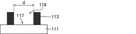
- FIG. 15 is a cross-sectional view schematically showing a BM manufactured by the method for manufacturing a color filter substrate of Comparative Embodiment 1.
- FIG. 16 is an SEM photograph showing a cross section of a BM manufactured by the method for manufacturing a color filter substrate of Comparative Example 1.
- FIG. 17 is a diagram schematically showing the manufacturing process of the color filter substrate of Comparative Embodiment 1, and shows the ink ejection process.
- the BM 113 functions as a partition wall that prevents the ink 118 from flowing. Also, as shown in FIG. 17, the ink 118 has a convex shape with a thick central portion. Then, the temporary baking (pre-baking) process and the main baking (post-baking) process were performed, and CF119 was formed.
- FIG. 18 shows a three-dimensional image of the CF 119 and the BM 113 by white interferometry.
- FIG. 19 is a graph showing the film thickness distribution of a certain CF119.
- the shape of each CF 119 is also convex, and the film thickness (shape) of each CF 119 is not uniform. Therefore, when the liquid crystal panel is assembled using the color filter substrate manufactured by the above method, the thickness of the liquid crystal layer becomes uneven in the sub-pixels. As a result, the optical characteristics of the liquid crystal display including the liquid crystal panel, that is, the display characteristics, were inferior compared to the case where CF was formed using a photolithography method.
- the inventor of the present invention has studied various methods for manufacturing a color filter substrate capable of improving the uniformity of the film thickness of the color filter, and has focused on the shape of the partition wall that prevents the ink from flowing. Then, in the photomask for forming the partition wall, a light transmitting region, a light shielding region, and a light control region having a transmittance smaller than the transmittance of the light transmitting region and larger than the transmittance of the light shielding region.
- the light control region is formed and provided between the light transmission region and the light shielding region along the contour lines of the light transmission region and the light shielding region, thereby corresponding to the light transmission region or the light shielding region.
- the inventors have found that the main body portion of the partition wall can be formed and that the rib portion of the partition wall can be formed corresponding to the light control region, and that the above problem can be solved brilliantly, and the present invention has been achieved.
- one aspect of the present invention is a method for manufacturing a color filter substrate, which includes (1) a step of forming a photoresist film, and (2) exposing the photoresist film through a photomask. The step of: (3) developing the exposed photoresist film to form a partition having an opening; and (4) ejecting ink into the opening.
- the light control region is a method for manufacturing a color filter substrate provided between the light transmitting region and the light shielding region along the contour lines of the light transmitting region and the light shielding region, respectively.
- the manufacturing method of the color filter substrate is not particularly limited by other steps as long as such steps are included as essential.
- a preferred embodiment of the method for manufacturing the color filter substrate will be described in detail below. The various forms shown below may be combined as appropriate.
- the translucent region does not necessarily need to completely transmit light of all wavelengths.
- the transmittance of the light transmitting region at a wavelength of 350 to 450 nm is preferably 90 to 95%.
- the light shielding region is not necessarily required to completely shield light of all wavelengths.
- the transmittance of the light shielding region at a wavelength of 350 to 450 nm is preferably 1% or less.
- the transmittance of the light control region at a wavelength of 350 to 450 nm is preferably 2 to 80%.
- the dimming area is preferably a halftone area or a gray tone area.
- the opening is a first opening
- a second opening is formed in the partition together with the first opening
- the partition includes a lower part, and An upper portion, the upper portion including a first overhanging portion projecting toward the first opening side and a second overhanging portion projecting toward the second opening side;
- the first ink is ejected, and a second ink having a color different from the first ink is ejected into the second opening, and the light control region Includes a form (hereinafter also referred to as a first form) provided to form the first overhang part and the second overhang part. According to this, it is possible to improve the film thickness uniformity of the color filters of a plurality of colors.
- regions is an area
- the transmittance (first transmittance) may be different or substantially the same. When the two are different from each other, it is possible to easily form a plurality of color filters having different film thicknesses and to easily optimize their shapes. When both are substantially the same, it is possible to easily form a plurality of color filters whose film thicknesses are substantially the same, and it is possible to easily optimize their shapes.
- the difference between the first transmittance and the second transmittance at a wavelength of 350 to 450 nm may be 1% or more, and when both are substantially the same, the wavelength is 350 to 450 nm.
- the difference between the first transmittance and the second transmittance in may be less than 1%.
- a color filter substrate including a substrate, a partition wall in which an opening is formed, and a color filter formed in the opening, wherein the color filter and the partition wall are the substrate.
- the partition Formed on the partition, the partition has a lower part and an upper part including a projecting part projecting to the opening side, the color filter has a shape projecting to the opposite side of the substrate, and the It is a color filter substrate in contact with the surface of the overhanging portion on the substrate side.
- the configuration of the color filter substrate is not particularly limited by other components as long as such components are formed as essential.
- a preferred embodiment of the color filter substrate will be described in detail below. The various forms shown below may be combined as appropriate.
- the opening, the color filter, and the overhang portion are a first opening, a first color filter, and a first overhang portion, respectively
- the partition wall includes a second
- the color filter substrate further includes a second color filter formed in the second opening and on the substrate, and the upper portion projects to the second opening side.
- the second color filter is different from the color of the first color filter, and the second color filter has a shape protruding to the opposite side of the substrate.
- a form hereinafter also referred to as a second form of contacting the surface of the second overhanging portion on the substrate side. According to this, it is possible to improve the film thickness uniformity of the color filters of a plurality of colors.
- the color filter board substrate which can improve the uniformity of the film thickness of a color filter, and its manufacturing method are realizable.
- FIG. 3 is a schematic plan view of a photomask used in the manufacturing process of the color filter substrate of Embodiment 1.
- FIG. 4 is an enlarged view of the photomask shown in FIG. 3 and shows a halftone region and a light shielding region.
- FIG. 4 is a schematic cross-sectional view taken along line A1-A2 in FIG. 3 is a schematic plan view of a partition wall produced by the method for producing a color filter substrate of Embodiment 1.
- FIG. 7 is a schematic cross-sectional view taken along line B1-B2 in FIG.
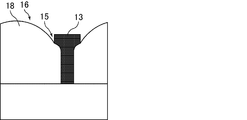
- FIG. 5 is a diagram schematically illustrating a manufacturing process of the color filter substrate of Embodiment 1 and illustrates an ink ejection process. It is a cross-sectional schematic diagram of the eaves part of the partition in FIG. 8, and its vicinity.
- 2 is a schematic cross-sectional view of a color filter substrate manufactured by the method for manufacturing a color filter substrate of Embodiment 1.
- FIG. 4 is another schematic cross-sectional view of a color filter substrate manufactured by the method for manufacturing a color filter substrate of Embodiment 1.
- FIG. 5 is a diagram schematically illustrating a manufacturing process of the color filter substrate of Embodiment 1 and illustrates an ink ejection process. It is a cross-sectional schematic diagram of the eaves part of the partition in FIG. 8, and its vicinity.
- 2 is a schematic cross-sectional view of a color filter substrate manufactured by the method for manufacturing a color filter
- FIG. 3 is a scanning electron microscope (SEM) photograph (reference photograph) showing a section of a partition wall produced by a method for producing a color filter substrate different from that in Embodiment 1.
- FIG. 6 is a schematic plan view of a photomask used in the manufacturing process of a color filter substrate of Embodiment 2.
- FIG. 6 is a schematic cross-sectional view of a color filter substrate manufactured by the method for manufacturing a color filter substrate of Embodiment 3. It is a cross-sectional schematic diagram of BM produced by the manufacturing method of the color filter substrate of the comparative form 1.
- 4 is a scanning electron microscope (SEM) photograph showing a cross section of a BM produced by the method for producing a color filter substrate of Comparative Embodiment 1.
- Embodiment 1 With reference to FIGS. 1 to 12, a method of manufacturing the color filter substrate of Embodiment 1 will be described.
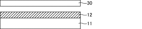
- a liquid or sheet-like photoresist material is applied or pasted on a transparent substrate 11 such as a glass substrate. Thereafter, if necessary, a preliminary baking step and a main baking step are performed in this order, and a light-shielding photoresist film 12 is formed as shown in FIG.
- the film thickness of the photoresist film 12 is 1.0 to 3.0 ⁇ m (preferably 2.0 to 2.5 ⁇ m).
- the photoresist material is negative.
- the color of a photoresist material and the partition mentioned later is not specifically limited, Black is preferable and it is preferable that a photoresist material and the partition mentioned later contain a black pigment. Thereby, an excellent contrast can be realized.
- the photoresist film 12 is irradiated with electromagnetic waves (for example, ultraviolet rays) through a photomask 30.
- the exposure dose at this time is, for example, 50 to 200 mJ / cm 2 (preferably 100 to 150 mJ / cm 2 ).
- the type of exposure apparatus that can be used in the present embodiment is not particularly limited, and examples include a stepper, a mirror projection exposure apparatus, and a proximity exposure apparatus.
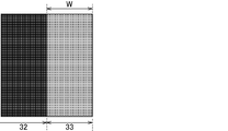
- the HT region 33 is provided between the light transmitting region 31 and the light shielding region 32 along the contour lines of the light transmitting region 31 and the light shielding region 32, respectively.
- the light shielding region 32 is provided in a rectangular shape.
- the light transmitting region 31 is a region other than the light shielding region 32 and the HT region 33, and the light transmitting region 31 is provided in a lattice shape. In this way, the HT region 33 is provided along the edge of the light shielding region 32.
- the HT region 33 borders one of the regions 31 and 32, and the other of the regions 31 and 32 corresponds to a region excluding one of the regions 31 and 32 and the HT region 33.
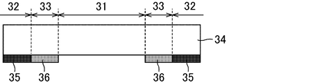
- the photomask 30 includes a transparent substrate (support) 34, a light shielding layer 35, and a semi-transmissive layer 36.
- the light shielding layer 35 and the semi-transmissive layer 36 are each patterned on the substrate 34.
- the light shielding layer 35 is formed by patterning a light shielding thin film.
- the light shielding layer 35 substantially completely blocks the irradiated light.
- the transmittance of the light shielding layer 35 at a wavelength of 350 to 450 nm is substantially 0%.
- Examples of the material of the light shielding layer 35 include metals such as chromium.
- the light shielding layer 35 is formed in the entire area of the light shielding area 32 and is not formed in the light transmitting area 31. Therefore, since only the substrate 34 exists in the light-transmitting region 31, the light-transmitting region 31 transmits almost the irradiated light.
- the light shielding region 32 substantially completely blocks the irradiated light.
- the semi-transmissive layer 36 is formed in the entire region of the HT region 33. Therefore, the HT region 33 transmits a part of the irradiated light.
- the photoresist pattern is irradiated with electromagnetic waves (for example, ultraviolet rays) or electron beams.
- electromagnetic waves for example, ultraviolet rays
- electron beams for example, electron beams
- a baking step is performed at 160 to 300 ° C. (preferably 200 to 260 ° C.).
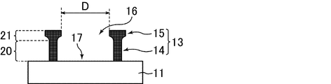
- a plurality of rectangular openings 16 are formed in the partition wall 13, and the partition wall 13 includes a lattice-shaped main body portion 14 and a hook portion (an overhang portion) 15.
- the eaves part 15 protrudes from the upper part of the main body part 14 (the part opposite to the substrate 11) toward the opening 16 (toward the opening 16).
- the partition wall 13 has a lower portion (a portion on the substrate 11 side) 20 and an upper portion (a portion on the side opposite to the substrate 11) 21 including the eaves portion 15.
- the eaves part 15 projects from the lower part 20 to the opening 16 side.
- the thickness of the eaves part 15, more specifically, the thickness of the part in contact with the main body part of the eaves part 15 is about 0.2 to 0.5 ⁇ m.
- the width of the eaves portion 15 is about 3 to 30 ⁇ m.
- the main body portion 14 is formed corresponding to a portion exposed through the light transmitting region 31 of the photoresist film 12, and the eaves portion 15 corresponds to a portion exposed through the HT region 33 of the photoresist film 12. Formed. An opening 16 is formed in the portion where the photoresist film 12 has been removed.
- the distance D between the mutually opposite elongate portions 15 is substantially equal to the distance d between the mutually opposing portions of the BM 113 of the first comparative example.
- the exposed part 17 (the part exposed in the opening 16) of the substrate 11 is made lyophilic (preferably hydrophilic).
- the surface of the partition wall 13 is made liquid repellent (preferably water repellent).
- a liquid repellent may be mixed into the photoresist material, but the photoresist material and the partition wall 13 preferably do not contain the liquid repellent.
- the ink 18 is in contact with the lower surface (the surface on the substrate 11 side, the surface facing the substrate 11) of the eaves portion 15. Thereby, the surface of the ink 18 is pushed into the substrate 11 side by the eaves portion 15. That is, pressure is applied to the ink 18 toward the substrate 11 side. As a result, the surface of the ink 18 can be made flatter than in the case of the comparative form 1. Further, it is possible to prevent the inks 18 of different colors from getting mixed over the partition wall 13. Further, the ink 18 does not spread to the partition wall 13, and a gap can be prevented from being generated between the color filter (CF) 19 described later and the partition wall 13.
- CF color filter
- the film thicknesses (heights) of the CFs of each color are substantially the same.
- the thicknesses of the CF color portions (the color portions 15R, the color portions 15G, and the color portions 15B) for the CFs of the respective colors are substantially the same, thereby facilitating the shape of each color CF having the above-described film thickness. Can be optimized.
- FIG. 12 shows an SEM photograph (reference photograph) showing a cross section of a partition wall produced by a method for producing a color filter substrate different from the present embodiment.
- the eaves portion 15 can be formed on the edge of the partition wall 13 in the same manner as the partition wall shown in FIG. Therefore, as described above, the surface of the ink 18 can be flattened. As a result, the surface of the CF 19 can be flattened, and the film thickness uniformity of the CF 19 can be improved.
- the CF 19 is formed using a photolithography method and has color performance (optical characteristics) equivalent to that of the CF. Therefore, when the color filter substrate 10 is used for a liquid crystal display, the liquid crystal display realizes optical characteristics (display characteristics) equivalent to those when a color filter substrate on which CF is formed using a photolithography method is used. Can do.
- the use of the color filter substrate 10 is not particularly limited, and examples thereof include FPD such as a liquid crystal display and an organic EL display.
- the number of exposures required for forming the partition wall 13 is one.
- the number of exposures required is two. That is, according to the present embodiment, it is possible to reduce the number of processes, that is, to reduce costs, as compared with the techniques described in Patent Documents 2 and 3.
- the photoresist material may be a positive type.
- the pattern of the light transmitting region 31 and the pattern of the light shielding region 32 may be interchanged.
- the photoresist material and the partition wall 13 may be transparent, but in that case, it is preferable to provide a light shielding film separately.
- the light shielding film may be formed by patterning a light shielding thin film (for example, a metal film such as chromium). Then, after forming the light shielding film, the transparent partition wall 13 may be formed.
- the type and number of colors of the CF 19 are not particularly limited and can be set as appropriate.
- the CF 19 may have four colors of red, blue, green, and yellow, may have four colors of red, blue, green, and colorless, or may have five colors of red, blue, green, yellow, and cyan. It may be a color, or may be three colors of yellow, cyan, and magenta.
- Embodiment 2 This embodiment is the same as Embodiment 1 except for the following points.
- the exposure process is performed using the photomask 230 instead of the photomask 30.
- the pattern of the translucent part of the GT region 237 is not particularly limited, and examples thereof include slits, dots, and fine patterns. Since the translucent part is smaller than the resolution limit of the exposure apparatus, the eaves part 15 can be formed without transferring the pattern of the translucent part. Therefore, according to this embodiment, the surface of the CF can be flattened, and the uniformity of the CF film thickness can be improved.
- Embodiment 3 This embodiment is the same as Embodiment 1 except for the following points.
- the settings of the type of light control region, the transmittance, the width, and the like are different for each CF color.
- the light control region of the photomask used in the present embodiment includes a plurality of regions in which at least one of the pattern type, the transmittance, and the width is different from each other.
- the shape (for example, thickness) of a eaves part can be optimized for every color of CF. This is because, usually, the optimum shape of the shade portion differs depending on the color (type) of the ink.
- the photomask used in this embodiment may have an HT region and a GT region.
- the transmittance can be easily varied between the HT region and the GT region. Therefore, the shape of the eaves portion can be optimized for each color more easily.
- Color filter substrate 11 Transparent substrate 12: Photoresist film 13: Partition wall 14: Main body portions 15, 15R, 15G, 15B, 315R, 315G, 315B: Hedge portion (overhang portion) 16: Opening 17: Exposed portion 18: Ink 19: Color filter (CF) 19R, 319R: Red color filter (CF) 19G, 319G: Green color filter (CF) 19B, 319B: Blue color filter (CF) 20: Lower part 21: Upper part 30, 230: Photomask 31: Translucent area 32: Light-shielding area 33: Halftone area (HT area) 34: Substrate (support) 35: Light-shielding layer 36: Transflective layer 237: Gray tone (GT) region
- GT Gray tone
Landscapes
- Physics & Mathematics (AREA)
- General Physics & Mathematics (AREA)
- Optics & Photonics (AREA)
- Nonlinear Science (AREA)
- Engineering & Computer Science (AREA)
- Manufacturing & Machinery (AREA)
- Mathematical Physics (AREA)
- Chemical & Material Sciences (AREA)
- Crystallography & Structural Chemistry (AREA)
- Optical Filters (AREA)
Abstract
本発明は、カラーフィルタの膜厚の均一性を向上することができるカラーフィルタ基板、及び、その製造方法を提供する。本発明は、カラーフィルタ基板の製造方法であって、前記製造方法は、フォトレジスト膜を形成する工程と、フォトマスクを介して前記フォトレジスト膜を露光する工程と、露光された前記フォトレジスト膜を現像することによって、開口を有する隔壁を形成する工程と、前記開口内にインクを吐出する工程とを含み、前記フォトマスクは、透光領域、遮光領域、及び、調光領域を有し、前記調光領域の透過率は、前記透光領域の透過率よりも小さく、かつ、前記遮光領域の透過率よりも大きく、前記調光領域は、前記透光領域、及び、前記遮光領域それぞれの輪郭線に沿って、前記透光領域、及び、前記遮光領域の間に設けられるカラーフィルタ基板の製造方法である。
Description
本発明は、カラーフィルタ基板、及び、その製造方法に関する。より詳しくは、インクジェット方式によってカラーフィルタを形成する場合に好適なカラーフィルタ基板、及び、その製造方法に関するものである。
カラーフィルタ基板は、液晶ディスプレイ等のフラットパネルディスプレイ(FPD)に広く利用されている。カラーフィルタ基板は、通常、透明基板、ブラックマトリクス(BM)、及び、カラーフィルタ(CF)を備える。BM、及び、CFは、透明基板上に形成される。
現在、CFは主にフォトリソグラフィ法を利用して形成される。しかしながら、インクジェット方式を用いてCFを形成する技術についても開発が進められている(例えば、特許文献1参照。)。インクジェット方式によれば、設備投資、及び、材料費の削減が可能であるので、カラーフィルタ基板のコストを削減することができる。また、インクジェット方式は、大型のカラーフィルタ基板にも容易に対応することができる。
また、インクジェット方式に用いられるBMの、形状、及び、撥液性を制御する技術が開示されている(例えば、特許文献2、3参照。)。これらでは、フォトリソグラフィ法を利用してBMが形成されており、BMを形成するために複数回の露光を行う必要がある。
ここで、図15~17を参照して、本発明者が検討を行った比較形態1のカラーフィルタ基板の製造方法について説明する。図15は、比較形態1のカラーフィルタ基板の製造方法によって作製されたBMを模式的に示した断面図である。図16は、比較形態1のカラーフィルタ基板の製造方法によって作製されたBMの断面を写したSEM写真である。図17は、比較形態1のカラーフィルタ基板の製造工程を模式的に示した図であり、インク吐出工程を示す。
まず、図15に示すように、透明基板111上に、フォトリソグラフィ法を用いて、開口116を有するBM113を形成した。BM113の断面形状は、図16に示すように、方形状又は台形状であった。次に、酸素を含む雰囲気下でプラズマ処理を行い、基板111の露出部117(開口116内において露出している部分)を親水化した。次に、CF4等のフッ素系ガスを用いたプラズマ処理を行い、BM113の表面を撥水化した。次に、インクジェット方式により、BM113の開口116内に、赤色、青色、緑色のインク118を吐出した。このとき、BM113は、インク118の流動を防止する隔壁として機能する。また、図17に示すように、インク118は、中央部が厚い凸形状になる。その後、仮焼成(プリベーク)工程、及び、本焼成(ポストベーク)工程を行い、CF119を形成した。
図18に、CF119、及び、BM113の白色干渉法による三次元画像を示す。図19は、ある一つのCF119の膜厚分布を示すグラフである。図18、19に示すように、比較形態1では、インク118同様、各CF119の形状も凸状であり、各CF119の膜厚(形状)が不均一であった。したがって、上記方法により作製されたカラーフィルタ基板を用いて液晶パネルを組み立てると、液晶層の厚みがサブ画素内で不均一になった。その結果、上記液晶パネルを備える液晶ディスプレイの光学特性、すなわち表示特性は、フォトリソグラフィ法を用いてCFを形成した場合に比べて劣っていた。
このように、インクジェット方式を採用した場合に、不均一な膜厚のCFが特に形成されやすい。
本発明は、上記現状に鑑みてなされたものであり、カラーフィルタの膜厚の均一性を向上することができるカラーフィルタ基板、及び、その製造方法を提供することを目的とするものである。
本発明者は、カラーフィルタの膜厚の均一性を向上することができるカラーフィルタ基板の製造方法について種々検討したところ、インクの流動を防止する隔壁の形状に着目した。そして、隔壁を形成するためのフォトマスクに、透光領域と、遮光領域と、透光領域の透過率よりも小さく、かつ、遮光領域の透過率よりも大きい透過率を有する調光領域とを形成し、この調光領域を、透光領域、及び、遮光領域それぞれの輪郭線に沿って、透光領域、及び、遮光領域の間に設けることにより、透光領域、又は、遮光領域に対応して隔壁の本体部分を形成でき、調光領域に対応して隔壁のヒサシ部を形成できることを見いだし、上記課題をみごとに解決することができることに想到し、本発明に到達したものである。
すなわち、本発明の一側面は、カラーフィルタ基板の製造方法であって、前記製造方法は、(1)フォトレジスト膜を形成する工程と、(2)フォトマスクを介して前記フォトレジスト膜を露光する工程と、(3)露光された前記フォトレジスト膜を現像することによって、開口を有する隔壁を形成する工程と、(4)前記開口内にインクを吐出する工程とを含み、前記フォトマスクは、透光領域、遮光領域、及び、調光領域を有し、前記調光領域の透過率は、前記透光領域の透過率よりも小さく、かつ、前記遮光領域の透過率よりも大きく、前記調光領域は、前記透光領域、及び、前記遮光領域それぞれの輪郭線に沿って、前記透光領域、及び、前記遮光領域の間に設けられるカラーフィルタ基板の製造方法である。
前記カラーフィルタ基板の製造方法は、このような工程を必須として含むものである限り、その他の工程により特に限定されるものではない。前記カラーフィルタ基板の製造方法における好ましい形態について以下に詳しく説明する。なお、以下に示す各種形態は、適宜、組み合わされてもよい。
前記透光領域は、必ずしも全波長の光を完全に透過する必要はない。波長350~450nmにおける前記透光領域の透過率は、好適には、90~95%である。
前記遮光領域は、必ずしも全波長の光を完全に遮光する必要はない。波長350~450nmにおける前記遮光領域の透過率は、好適には、1%以下である。
波長350~450nmにおける前記調光領域の透過率は、好適には、2~80%である。
前記調光領域は、ハーフトーン領域、又は、グレートーン領域であることが好ましい。これにより、調光領域の透過率を、より容易、かつ、より確実に、透光領域の透過率よりも小さく、かつ、遮光領域の透過率よりも大きくすることができる。したがって、より容易、かつ、より確実に、本発明を実現することができる。
前記隔壁は、下部と、前記開口側に張り出した張出し部を含む上部とを有することが好ましく、前記工程(4)において、前記インクは、前記張出し部の前記基板側の面に接するまで吐出されることが好ましい。
他の好ましい形態としては、前記開口は、第一の開口であり、前記工程(3)において、前記第一の開口とともに第二の開口を前記隔壁に形成し、前記隔壁は、下部、及び、上部を有し、前記上部は、前記第一の開口側に張り出した第一の張出し部と、前記第二の開口側に張り出した第二の張出し部とを含み、前記インクは、第一のインクであり、前記工程(4)において、前記第一のインクを吐出するとともに、前記第二の開口内に前記第一のインクとは異なる色の第二のインクを吐出し、前記調光領域は、前記第一の張出し部、及び、第二の張出し部を形成するために設けられる形態(以下、第一の形態とも言う。)が挙げられる。これによれば、複数色のカラーフィルタの膜厚の均一性を向上することができる。
上記第一の形態では、前記調光領域のうち、前記第二の張出し部を形成するための領域の透過率(第二の透過率)が、前記第一の張出し部を形成するための領域の透過率(第一の透過率)と、異なっていてもよいし、又は、実質的に同じであってもよい。両者が互いに異なっている場合は、互いに膜厚が異なる複数色のカラーフィルタを容易に形成でき、また、それらの形状を容易に最適化することができる。両者が互いに実質的に同じ場合は、互いの膜厚が実質的に同じである複数色のカラーフィルタを容易に形成でき、また、それらの形状を容易に最適化することができる。両者が互いに異なっている場合、波長350~450nmにおける第一の透過率と第二の透過率の差は、1%以上であってもよく、両者が互いに実質的に同じ場合、波長350~450nmにおける第一の透過率と第二の透過率の差は、1%未満であってもよい。
本発明の他の側面は、基板と、開口が形成された隔壁と、前記開口内に形成されたカラーフィルタとを備えるカラーフィルタ基板であって、前記カラーフィルタ、及び、前記隔壁は、前記基板上に形成され、前記隔壁は、下部と、前記開口側に張り出した張出し部を含む上部とを有し、前記カラーフィルタは、前記基板とは反対側に突出した形状を有し、かつ、前記張出し部の前記基板側の面に接するカラーフィルタ基板である。
前記カラーフィルタ基板は、前記カラーフィルタ基板の製造方法を用いて作製することができる。したがって、カラーフィルタの膜厚の均一性を向上することができる。
前記カラーフィルタ基板の構成としては、このような構成要素を必須として形成されるものである限り、その他の構成要素により特に限定されるものではない。前記カラーフィルタ基板における好ましい形態について以下に詳しく説明する。なお、以下に示す各種形態は、適宜、組み合わされてもよい。
前記隔壁は、撥液剤を含まないことが好ましい。これにより、隔壁の形成工程後に、隔壁の表面処理工程を実施することができる。したがって、隔壁の表面の性質を任意の性質(親液性、又は、撥液性)に設定することができる。
他の好ましい形態としては、前記開口、前記カラーフィルタ、及び、前記張出し部はそれぞれ、第一の開口、第一のカラーフィルタ、及び、第一の張出し部であり、前記隔壁には、第二の開口が更に形成され、前記カラーフィルタ基板は、前記第二の開口内、かつ、前記基板上に形成された第二のカラーフィルタを更に備え、前記上部は、前記第二の開口側に張り出した第二の張出し部を更に有し、前記第二のカラーフィルタの色は、前記第一のカラーフィルタの色と異なり、前記第二のカラーフィルタは、前記基板とは反対側に突出した形状を有し、かつ、前記第二の張出し部の前記基板側の面に接する形態(以下、第二の形態とも言う。)が挙げられる。これによれば、複数色のカラーフィルタの膜厚の均一性を向上することができる。
上記第二の形態では、前記第二の張出し部の厚み(第二の厚み)は、前記第一の張出し部の厚み(第一の厚み)と、異なっていてもよいし、又は、実質的に同じであってもよい。両者が互いに異なっている場合は、互いに膜厚が異なる複数色のカラーフィルタを容易に形成でき、また、それらの形状を容易に最適化することができる。両者が互いに実質的に同じ場合は、互いの膜厚が実質的に同じである複数色のカラーフィルタを容易に形成でき、また、それらの形状を容易に最適化することができる。両者が互いに異なっている場合、第一の厚みと第二の厚みの差は、0.1μm以上であってもよく、両者が互いに実質的に同じ場合、第一の厚みと第二の厚みの差は、0.1μm未満であってもよい。
本発明によれば、カラーフィルタの膜厚の均一性を向上することができるカラーフィルタ基板、及び、その製造方法を実現することができる。
以下に実施形態を掲げ、本発明を図面を参照して更に詳細に説明するが、本発明はこれらの実施形態のみに限定されるものではない。
(実施形態1)
図1~12を参照して、実施形態1のカラーフィルタ基板の製造方法について説明する。
図1~12を参照して、実施形態1のカラーフィルタ基板の製造方法について説明する。
まず、ガラス基板等の透明基板11上に、液状、又は、シート状のフォトレジスト材料を塗布、又は、貼付する。その後、必要に応じて、仮焼成工程、及び、本焼成工程をこの順に行い、図1に示すように、遮光性のフォトレジスト膜12を形成する。
フォトレジスト膜12の膜厚は、1.0~3.0μm(好適には2.0~2.5μm)である。フォトレジスト材料は、ネガ型である。なお、フォトレジスト材料、及び、後述する隔壁の色は特に限定されないが、黒色が好ましく、フォトレジスト材料、及び、後述する隔壁は、黒色顔料を含むことが好ましい。これにより、優れたコントラストを実現することができる。
次に、図2に示すように、フォトマスク30を介して、電磁波(例えば、紫外線)をフォトレジスト膜12に照射する。このときの露光量は、例えば、50~200mJ/cm2(好適には100~150mJ/cm2)である。
本実施形態において使用可能な露光装置の種類は特に限定されず、例えば、ステッパ、ミラープロジェクション露光装置、プロキシミティ露光装置等が挙げられる。
また、電磁波の代わりに電子線を照射してもよい。
フォトマスク30は、図3、4に示すように、透光領域31と、遮光領域32と、調光領域であるハーフトーン領域(HT領域)33とを有する。
HT領域33は、透光領域31、及び、遮光領域32それぞれの輪郭線に沿って、透光領域31、及び、遮光領域32の間に設けられている。遮光領域32は、矩形状に設けられている。透光領域31は、遮光領域32、及び、HT領域33以外の領域であり、透光領域31は、格子状に設けられている。このように、HT領域33は、遮光領域32のエッジに沿って設けられている。また、HT領域33は、領域31、32の一方を縁取り、領域31、32の他方は、領域31、32の一方と、HT領域33とを除く領域に対応している。
HT領域33の幅Wは、0.5~10μm(好適には1.0~3.0μm)である。
図5に示すように、フォトマスク30は、透明な基板(支持体)34、遮光層35、及び、半透過層36を有する。遮光層35、及び、半透過層36はそれぞれ、基板34上にパターニングされている。
基板34は、照射された光を実質的に全て透過する。具体的には、波長350~450nmにおける基板34の透過率は、実質的に92%である。基板34の材料としては、ソーダ石灰ガラス、合成石英ガラス等のガラスが挙げられる。
遮光層35は、遮光性の薄膜をパターニングすることによって形成される。遮光層35は、照射された光を実質的に完全に遮断する。具体的には、波長350~450nmにおける遮光層35の透過率は、実質的に0%である。遮光層35の材料としては、クロム等の金属が挙げられる。
遮光層35は、遮光領域32の全領域内に形成され、透光領域31内には形成されていない。したがって、透光領域31内には、基板34のみが存在するので、透光領域31は、照射された光をほとんど透過する。また、遮光領域32は、照射された光を実質的に完全に遮断する。
半透過層36は、半透過性の薄膜をパターニングすることによって形成される。半透過層36は、照射された光の一部を透過する。具体的には、波長350~450nmにおける半透過層36の透過率は、例えば、20%(好適には30%)以上、80%(好適には70%)以下である。半透過層36の材料としては、クロム、モリブデンシリサイド、タンタル、アルミニウム、ケイ素等の元素を含む酸化物、窒化物、炭化物、酸窒化物、炭窒化物等が挙げられる。
半透過層36は、HT領域33の全領域内に形成されている。したがって、HT領域33は、照射された光の一部を透過する。
透光領域31、遮光領域32、及び、HT領域33の透過率はそれぞれ、基板34、遮光層35、及び、半透過層36の透過率と同じである。したがって、フォトマスク30の透過率は、遮光領域32、HT領域33、及び、透光領域31の順で大きくなる。
次に、水酸化カリウム水溶液等の現像液を用いて、露光されたフォトレジスト膜12を現像し、フォトレジストパターンを形成する。これにより、フォトレジスト膜12の透光領域31を介して露光された部分は、ほとんど残存する。それに対して、フォトレジスト膜12のHT領域33を介して露光された部分は、部分的に除去され、フォトレジスト膜12の遮光領域32に対応する部分、すなわち未露光部分は、実質的に全て除去される。
次に、電磁波(例えば、紫外線)又は電子線を、フォトレジストパターンに照射する。
次に、160~300℃(好適には200~260℃)で焼成工程を行う。
以上の工程によって、図6、7に示すように、基板11上に隔壁(バンク)13が形成される。
隔壁13には、矩形状の複数の開口16が形成され、隔壁13は、格子状の本体部分14と、ヒサシ部(張出し部)15とを含む。ヒサシ部15は、本体部分14の上部(基板11とは反対側の部分)から開口16側に(開口16に向かって)突き出ている。換言すると、隔壁13は、下部(基板11側の部分)20と、ヒサシ部15を含む上部(基板11とは反対側の部分)21とを有する。ヒサシ部15は、下部20よりも開口16側に張り出している。ヒサシ部15の厚み、より詳細には、ヒサシ部15の本体部分に接する部分の厚みは、0.2~0.5μm程度である。また、ヒサシ部15の幅は、3~30μm程度である。
本体部分14は、フォトレジスト膜12の透光領域31を介して露光された部分に対応して形成され、ヒサシ部15は、フォトレジスト膜12のHT領域33を介して露光された部分に対応して形成される。また、フォトレジスト膜12が除去された部分に開口16が形成されている。
すなわち、フォトマスク30の遮光領域32は、開口16に対応して、開口16を形成するために設けられ、透光領域31は、本体部分14に対応して、本体部分14を形成するために設けられ、HT領域33は、ヒサシ部15に対応して、ヒサシ部15を形成するために設けられている。
なお、図7、15に示すように、互いに対向するヒサシ部15の間の距離Dは、比較形態1のBM113の互いに対向する部分の間の距離dと略等しい。
次に、酸素を含む雰囲気下でプラズマ処理を行う。これにより、基板11の露出部17(開口16内において露出している部分)を親液性(好適には親水性)にする。
次に、CF4等のフッ素系ガスを用いたプラズマ処理を行う。これにより、隔壁13の表面を撥液性(好適には撥水性)にする。なお、プラズマ処理を行う代わりに、フォトレジスト材料に撥液剤を混入してもよいが、フォトレジスト材料及び隔壁13は、撥液剤を含有しないことが好ましい。
次に、インクジェット装置を用いて、開口16内、すなわち露出部17上に、赤色、青色、緑色のインク18を吐出する。図8に示すように、インク18は、隔壁13によって堰き止められるまで、開口16内を広がり、その結果、開口16内はインク18によって満たされることになる。このように、隔壁13は、インク18の流動を防止する機能と、ブラックマトリクスとしての機能とを有する。また、インク18は、表面張力の影響によって、基板11とは反対側に突出した形状(凸形状)を有する。インク18の頂点は、隔壁13よりも非常に高くなっており、基板11の表面からインク18の頂点までの高さは、10~15μm程度であり、隔壁13の高さの5倍以上、20倍以下である。
また、図9に示すように、インク18は、ヒサシ部15の下面(基板11側の面、基板11に対向する面)に接している。これにより、インク18の表面は、ヒサシ部15によって基板11側に押し込まれる。すなわち、インク18には基板11側に向かって圧力が加わる。その結果、比較形態1の場合に比べて、インク18の表面をより平坦にすることができる。また、異なる色のインク18同士が隔壁13を乗り越えて混ざり合うのを防止することができる。更に、インク18が隔壁13まで広がらず、後述するカラーフィルタ(CF)19と、隔壁13との間に隙間が発生するのを防ぐことができる。
次に、仮焼成工程、及び、本焼成工程をこの順に行う。これにより、インク18中の溶媒が蒸発し、図10に示すように、赤色、青色、緑色のCF19が形成される。CF19は、隔壁13によって区画されている。このようにして、カラーフィルタ基板10が完成する。
CF19は、基板11とは反対側に突出した形状(凸形状)を有する。CF19は、溶媒が蒸発した分だけインク18よりも薄くなっているが、ヒサシ部15の下面には接している。
図11に示すように、各色のCF(赤色のCF19R、緑色のCF19G、青色のCF19B)の膜厚(高さ)は、互いに略同一である。また、各色のCF用のヒサシ部(ヒサシ部15R、ヒサシ部15G、ヒサシ部15B)の厚みは、互いに略同一であり、これにより、上述のような膜厚を有する各色のCFの形状を容易に最適化することができる。
図12に、本実施形態とは異なるカラーフィルタ基板の製造方法によって作製された隔壁の断面を写したSEM写真(参考写真)を示す。本実施形態によっても、図12に示した隔壁と同様に、隔壁13のエッジにヒサシ部15を形成することができる。したがって、上述のように、インク18の表面を平坦にすることができる。その結果、CF19の表面も平坦にでき、CF19の膜厚の均一性を向上することができる。
また、CF19は、フォトリソグラフィ法を利用して形成されCFと同等の色性能(光学特性)を有する。そのため、カラーフィルタ基板10を液晶ディスプレイに利用した場合、この液晶ディスプレイは、フォトリソグラフィ法を用いてCFが形成されたカラーフィルタ基板を利用した場合と同等の光学特性(表示特性)を実現することができる。
なお、カラーフィルタ基板10の用途は特に限定されず、例えば、液晶ディスプレイ、有機ELディスプレイ等のFPDが挙げられる。
また、本実施形態において、隔壁13の形成のために必要な露光回数は1回であり、上述の特許文献2、3に記載の技術では、必要な露光回数は2回である。すなわち、本実施形態によれば、特許文献2、3に記載の技術に比べて、工程数の削減、すなわちコストの削減が可能である。
また、本実施形態では、隔壁13の形成工程後に、隔壁13の表面処理工程を実施している。そのため、隔壁13の表面の性質を任意の性質(親液性、又は、撥液性)に設定することができる。他方、特許文献2、3に記載の技術では、撥液剤(撥インク剤)を含有するBM用樹脂組成物を使用している。このような製造プロセスの相違により、特許文献2、3に記載の技術では、本実施形態のようにCF19の表面を平坦にすることができない。
なお、本実施形態において、フォトレジスト材料は、ポジ型であってもよい。この場合、透光領域31のパターンと、遮光領域32のパターンを互いに入れ替えればよい。
また、フォトレジスト材料、及び、隔壁13は、透明であってもよいが、その場合は、別途、遮光膜を設けることが好ましい。なお、この遮光膜は、遮光性の薄膜(例えば、クロム等の金属膜)をパターニングすることによって形成すればよい。そして、遮光膜の形成後、透明な隔壁13を形成すればよい。
また、CF19の色の種類と数は特に限定されず、適宜設定することができる。例えば、CF19は、赤色、青色、緑色、黄色の4色であってもよいし、赤色、青色、緑色、無色の4色であってもよいし、赤色、青色、緑色、黄色、シアンの5色であってもよいし、黄色、シアン、マゼンタの3色であってもよい。
(実施形態2)
本実施形態は、以下の点を除いて、実施形態1と同じである。
本実施形態においては、フォトマスク30の代わりに、フォトマスク230を用いて露光工程を行う。
本実施形態は、以下の点を除いて、実施形態1と同じである。
本実施形態においては、フォトマスク30の代わりに、フォトマスク230を用いて露光工程を行う。
図13に示すように、フォトマスク230は、HT領域33の代わりに、調光領域としてグレートーン(GT)領域237を有することを除いて、フォトマスク30と同じである。GT領域237には、遮光部と、露光装置の解像限界よりも小さい透光部とが形成されている。遮光部は、遮光領域32と同様に遮光層を含む。すなわち、遮光部は、上述の遮光性の薄膜を用いて形成される。透光部は、遮光層を含まず、基板34のみを含む。したがって、透光部は、照射された光をほとんど透過する。一方、遮光部は、遮光層を含むので、照射された光を実質的に完全に遮断する。すなわち、GT領域237は、照射された光の一部を透過する。
波長350~450nmにおけるGT領域237の透過率は、実質的に数%である。したがって、フォトマスク230の透過率は、遮光領域32、GT領域237、及び、透光領域31の順で大きくなる。
GT領域237の透光部のパターンは特に限定されず、例えば、スリット、ドット、微細パターン等が挙げられる。透光部は、露光装置の解像限界よりも小さいので、透光部のパターンが転写されること無く、ヒサシ部15を形成することができる。したがって、本実施形態によっても、CFの表面も平坦にでき、CFの膜厚の均一性を向上することができる。
(実施形態3)
本実施形態は、以下の点を除いて、実施形態1と同じである。
本実施形態の露光工程に用いられるフォトマスクにおいては、CFの色毎に、調光領域の種類、透過率、幅などの設定が互いに異なる。換言すると、本実施形態に用いられるフォトマスクの調光領域は、パターンの種類と、透過率と、幅との少なくとも一つが互いに異なる複数の領域を含む。これにより、ヒサシ部の形状(例えば、厚み)をCFの色毎で最適化することができる。通常、インクの色(種類)によって、ヒサシ部の最適な形状は異なるためである。
本実施形態は、以下の点を除いて、実施形態1と同じである。
本実施形態の露光工程に用いられるフォトマスクにおいては、CFの色毎に、調光領域の種類、透過率、幅などの設定が互いに異なる。換言すると、本実施形態に用いられるフォトマスクの調光領域は、パターンの種類と、透過率と、幅との少なくとも一つが互いに異なる複数の領域を含む。これにより、ヒサシ部の形状(例えば、厚み)をCFの色毎で最適化することができる。通常、インクの色(種類)によって、ヒサシ部の最適な形状は異なるためである。
例えば、本実施形態に用いられるフォトマスクは、HT領域及びGT領域を有してもよい。これにより、HT領域と、GT領域とで透過率を容易に異ならせることができる。そのため、より容易に、ヒサシ部の形状を色毎で最適化することができる。
また、本実施形態では、各色のCFの膜厚(高さ)は、互いに異なる。より詳細には、各色のCFの平均膜厚、及び、最大膜厚(頂点部の膜厚)は、互いに異なる。更に、各色のCF用のヒサシ部の厚みも、互いに異なり、各色のCF用のヒサシ部の本体部分に接する部分の厚みは、0.2~0.5μm程度の範囲内で設定される。例えば、図14に示すように、緑色のCF319Gは、赤色のCF319Rよりも厚く、青色のCF319Bは、CF319Gよりも厚い。また、緑色のCF用のヒサシ部315Gは、青色のCF用のヒサシ部315Bよりも厚く、赤色のCF用のヒサシ部315Rは、ヒサシ部315Gよりも厚い。ヒサシ部315R、315G、315Bを形成することによって、上述のような膜厚を有する各色のCFの形状を容易に最適化することができる。
本願は、2010年11月2日に出願された日本国特許出願2010-246586号を基礎として、パリ条約ないし移行する国における法規に基づく優先権を主張するものである。該出願の内容は、その全体が本願中に参照として組み込まれている。
10:カラーフィルタ基板
11:透明基板
12:フォトレジスト膜
13:隔壁
14:本体部分
15、15R、15G、15B、315R、315G、315B:ヒサシ部(張出し部)
16:開口
17:露出部
18:インク
19:カラーフィルタ(CF)
19R、319R:赤色のカラーフィルタ(CF)
19G、319G:緑色のカラーフィルタ(CF)
19B、319B:青色のカラーフィルタ(CF)
20:下部
21:上部
30、230:フォトマスク
31:透光領域
32:遮光領域
33:ハーフトーン領域(HT領域)
34:基板(支持体)
35:遮光層
36:半透過層
237:グレートーン(GT)領域
11:透明基板
12:フォトレジスト膜
13:隔壁
14:本体部分
15、15R、15G、15B、315R、315G、315B:ヒサシ部(張出し部)
16:開口
17:露出部
18:インク
19:カラーフィルタ(CF)
19R、319R:赤色のカラーフィルタ(CF)
19G、319G:緑色のカラーフィルタ(CF)
19B、319B:青色のカラーフィルタ(CF)
20:下部
21:上部
30、230:フォトマスク
31:透光領域
32:遮光領域
33:ハーフトーン領域(HT領域)
34:基板(支持体)
35:遮光層
36:半透過層
237:グレートーン(GT)領域
Claims (9)
- カラーフィルタ基板の製造方法であって、
前記製造方法は、(1)フォトレジスト膜を形成する工程と、
(2)フォトマスクを介して前記フォトレジスト膜を露光する工程と、
(3)露光された前記フォトレジスト膜を現像することによって、開口を有する隔壁を形成する工程と、
(4)前記開口内にインクを吐出する工程とを含み、
前記フォトマスクは、透光領域、遮光領域、及び、調光領域を有し、
前記調光領域の透過率は、前記透光領域の透過率よりも小さく、かつ、前記遮光領域の透過率よりも大きく、
前記調光領域は、前記透光領域、及び、前記遮光領域それぞれの輪郭線に沿って、前記透光領域、及び、前記遮光領域の間に設けられる
ことを特徴とするカラーフィルタ基板の製造方法。 - 前記調光領域は、ハーフトーン領域、又は、グレートーン領域であることを特徴とする請求項1記載のカラーフィルタ基板の製造方法。
- 前記隔壁は、下部と、前記開口側に張り出した張出し部を含む上部とを有し、
前記工程(4)において、前記インクは、前記張出し部の前記基板側の面に接するまで吐出されることを特徴とする請求項1又は2記載のカラーフィルタ基板の製造方法。 - 前記開口は、第一の開口であり、
前記工程(3)において、前記第一の開口とともに第二の開口を前記隔壁に形成し、
前記隔壁は、下部、及び、上部を有し、
前記上部は、前記第一の開口側に張り出した第一の張出し部と、前記第二の開口側に張り出した第二の張出し部とを含み、
前記インクは、第一のインクであり、
前記工程(4)において、前記第一のインクを吐出するとともに、前記第二の開口内に前記第一のインクとは異なる色の第二のインクを吐出し、
前記調光領域は、前記第一の張出し部、及び、第二の張出し部を形成するために設けられ、
前記調光領域のうち、前記第二の張出し部を形成するための領域の透過率は、前記第一の張出し部を形成するための領域の透過率と異なることを特徴とする請求項1又は2記載のカラーフィルタ基板の製造方法。 - 前記開口は、第一の開口であり、
前記工程(3)において、前記第一の開口とともに第二の開口を前記隔壁に形成し、
前記隔壁は、下部、及び、上部を有し、
前記上部は、前記第一の開口側に張り出した第一の張出し部と、前記第二の開口側に張り出した第二の張出し部とを含み、
前記インクは、第一のインクであり、
前記工程(4)において、前記第一のインクを吐出するとともに、前記第二の開口内に前記第一のインクとは異なる色の第二のインクを吐出し、
前記調光領域は、前記第一の張出し部、及び、第二の張出し部を形成するために設けられ、
前記調光領域のうち、前記第二の張出し部を形成するための領域の透過率は、前記第一の張出し部を形成するための領域の透過率と実質的に同じであることを特徴とする請求項1又は2記載のカラーフィルタ基板の製造方法。 - 基板と、開口が形成された隔壁と、前記開口内に形成されたカラーフィルタとを備えるカラーフィルタ基板であって、
前記カラーフィルタ、及び、前記隔壁は、前記基板上に形成され、
前記隔壁は、下部と、前記開口側に張り出した張出し部を含む上部とを有し、
前記カラーフィルタは、前記基板とは反対側に突出した形状を有し、かつ、前記張出し部の前記基板側の面に接することを特徴とするカラーフィルタ基板。 - 前記隔壁は、撥液剤を含まないことを特徴とする請求項6記載のカラーフィルタ基板。
- 前記開口、前記カラーフィルタ、及び、前記張出し部はそれぞれ、第一の開口、第一のカラーフィルタ、及び、第一の張出し部であり、
前記隔壁には、第二の開口が更に形成され、
前記カラーフィルタ基板は、前記第二の開口内、かつ、前記基板上に形成された第二のカラーフィルタを更に備え、
前記上部は、前記第二の開口側に張り出した第二の張出し部を更に有し、
前記第二のカラーフィルタの色は、前記第一のカラーフィルタの色と異なり、
前記第二のカラーフィルタは、前記基板とは反対側に突出した形状を有し、かつ、前記第二の張出し部の前記基板側の面に接し、
前記第二の張出し部の厚みは、前記第一の張出し部の厚みと異なることを特徴とする請求項6又は7記載のカラーフィルタ基板。 - 前記開口、前記カラーフィルタ、及び、前記張出し部はそれぞれ、第一の開口、第一のカラーフィルタ、及び、第一の張出し部であり、
前記隔壁には、第二の開口が更に形成され、
前記カラーフィルタ基板は、前記第二の開口内、かつ、前記基板上に形成された第二のカラーフィルタを更に備え、
前記上部は、前記第二の開口側に張り出した第二の張出し部を更に有し、
前記第二のカラーフィルタの色は、前記第一のカラーフィルタの色と異なり、
前記第二のカラーフィルタは、前記基板とは反対側に突出した形状を有し、かつ、前記第二の張出し部の前記基板側の面に接し、
前記第二の張出し部の厚みは、前記第一の張出し部の厚みと実質的に同じであることを特徴とする請求項6又は7記載のカラーフィルタ基板。
Priority Applications (1)
| Application Number | Priority Date | Filing Date | Title |
|---|---|---|---|
| US13/881,922 US20130222936A1 (en) | 2010-11-02 | 2011-10-25 | Color filter substrate and method for producing same |
Applications Claiming Priority (2)
| Application Number | Priority Date | Filing Date | Title |
|---|---|---|---|
| JP2010246586 | 2010-11-02 | ||
| JP2010-246586 | 2010-11-02 |
Publications (1)
| Publication Number | Publication Date |
|---|---|
| WO2012060243A1 true WO2012060243A1 (ja) | 2012-05-10 |
Family
ID=46024360
Family Applications (1)
| Application Number | Title | Priority Date | Filing Date |
|---|---|---|---|
| PCT/JP2011/074483 Ceased WO2012060243A1 (ja) | 2010-11-02 | 2011-10-25 | カラーフィルタ基板、及び、その製造方法 |
Country Status (2)
| Country | Link |
|---|---|
| US (1) | US20130222936A1 (ja) |
| WO (1) | WO2012060243A1 (ja) |
Cited By (4)
| Publication number | Priority date | Publication date | Assignee | Title |
|---|---|---|---|---|
| CN102830457A (zh) * | 2012-08-13 | 2012-12-19 | 深超光电(深圳)有限公司 | 一种彩色滤光片基板 |
| WO2014030581A1 (ja) * | 2012-08-21 | 2014-02-27 | シャープ株式会社 | カラーフィルタ基板、及び、その製造方法 |
| JP2020160390A (ja) * | 2019-03-28 | 2020-10-01 | 凸版印刷株式会社 | ブラックマトリクス、カラーフィルタ、表示装置およびブラックマトリクスの製造方法 |
| CN115712203A (zh) * | 2022-10-27 | 2023-02-24 | 福建华佳彩有限公司 | 一种可提升亮度的微透镜彩膜基板的制备方法 |
Families Citing this family (4)
| Publication number | Priority date | Publication date | Assignee | Title |
|---|---|---|---|---|
| KR20150058910A (ko) * | 2013-11-21 | 2015-05-29 | 삼성디스플레이 주식회사 | 표시 장치 및 이의 제조 방법 |
| CN105717737B (zh) * | 2016-04-26 | 2019-08-02 | 深圳市华星光电技术有限公司 | 一种掩膜版及彩色滤光片基板的制备方法 |
| CN105892142A (zh) * | 2016-06-29 | 2016-08-24 | 武汉华星光电技术有限公司 | 黑色矩阵光罩、制备黑色矩阵的方法及其应用 |
| US20220406654A1 (en) * | 2021-06-18 | 2022-12-22 | Intel Corporation | Technologies for aligned vias |
Citations (7)
| Publication number | Priority date | Publication date | Assignee | Title |
|---|---|---|---|---|
| JP2003161826A (ja) * | 2001-11-29 | 2003-06-06 | Matsushita Electric Ind Co Ltd | カラーフィルタ及び液晶表示素子 |
| WO2007088690A1 (ja) * | 2006-01-31 | 2007-08-09 | Kyocera Corporation | El装置 |
| JP2008091071A (ja) * | 2006-09-29 | 2008-04-17 | Seiko Epson Corp | 電気光学装置、およびその製造方法 |
| JP2009145650A (ja) * | 2007-12-14 | 2009-07-02 | Toppan Printing Co Ltd | カラーフィルター、パターニング基板及びその製造方法 |
| JP2009145910A (ja) * | 2009-03-25 | 2009-07-02 | Toppan Printing Co Ltd | カラーフィルター、パターニング基板及びその製造方法 |
| JP2010020146A (ja) * | 2008-07-11 | 2010-01-28 | Fujifilm Corp | カラーフィルタ及びその製造方法、並びに液晶表示装置 |
| JP2010217390A (ja) * | 2009-03-16 | 2010-09-30 | Toppan Printing Co Ltd | 隔壁パターンの製造方法、カラーフィルタ、及び液晶表示装置 |
Family Cites Families (1)
| Publication number | Priority date | Publication date | Assignee | Title |
|---|---|---|---|---|
| US8329067B2 (en) * | 2006-04-03 | 2012-12-11 | Dai Nippon Printing Co., Ltd. | Method of producing color filter and color filter |
-
2011
- 2011-10-25 US US13/881,922 patent/US20130222936A1/en not_active Abandoned
- 2011-10-25 WO PCT/JP2011/074483 patent/WO2012060243A1/ja not_active Ceased
Patent Citations (7)
| Publication number | Priority date | Publication date | Assignee | Title |
|---|---|---|---|---|
| JP2003161826A (ja) * | 2001-11-29 | 2003-06-06 | Matsushita Electric Ind Co Ltd | カラーフィルタ及び液晶表示素子 |
| WO2007088690A1 (ja) * | 2006-01-31 | 2007-08-09 | Kyocera Corporation | El装置 |
| JP2008091071A (ja) * | 2006-09-29 | 2008-04-17 | Seiko Epson Corp | 電気光学装置、およびその製造方法 |
| JP2009145650A (ja) * | 2007-12-14 | 2009-07-02 | Toppan Printing Co Ltd | カラーフィルター、パターニング基板及びその製造方法 |
| JP2010020146A (ja) * | 2008-07-11 | 2010-01-28 | Fujifilm Corp | カラーフィルタ及びその製造方法、並びに液晶表示装置 |
| JP2010217390A (ja) * | 2009-03-16 | 2010-09-30 | Toppan Printing Co Ltd | 隔壁パターンの製造方法、カラーフィルタ、及び液晶表示装置 |
| JP2009145910A (ja) * | 2009-03-25 | 2009-07-02 | Toppan Printing Co Ltd | カラーフィルター、パターニング基板及びその製造方法 |
Cited By (6)
| Publication number | Priority date | Publication date | Assignee | Title |
|---|---|---|---|---|
| CN102830457A (zh) * | 2012-08-13 | 2012-12-19 | 深超光电(深圳)有限公司 | 一种彩色滤光片基板 |
| WO2014030581A1 (ja) * | 2012-08-21 | 2014-02-27 | シャープ株式会社 | カラーフィルタ基板、及び、その製造方法 |
| US9279924B2 (en) | 2012-08-21 | 2016-03-08 | Sharp Kabushiki Kaisha | Color filter substrate and method for producing same |
| JP2020160390A (ja) * | 2019-03-28 | 2020-10-01 | 凸版印刷株式会社 | ブラックマトリクス、カラーフィルタ、表示装置およびブラックマトリクスの製造方法 |
| JP7326812B2 (ja) | 2019-03-28 | 2023-08-16 | 凸版印刷株式会社 | ブラックマトリクス、カラーフィルタ、表示装置およびブラックマトリクスの製造方法 |
| CN115712203A (zh) * | 2022-10-27 | 2023-02-24 | 福建华佳彩有限公司 | 一种可提升亮度的微透镜彩膜基板的制备方法 |
Also Published As
| Publication number | Publication date |
|---|---|
| US20130222936A1 (en) | 2013-08-29 |
Similar Documents
| Publication | Publication Date | Title |
|---|---|---|
| WO2012060243A1 (ja) | カラーフィルタ基板、及び、その製造方法 | |
| KR100733480B1 (ko) | 그레이 톤 마스크의 제조 방법 | |
| JP5200439B2 (ja) | カラーフィルタの製造方法 | |
| KR101799860B1 (ko) | 위상 시프터 패턴이 형성된 공간 필터를 구비하는 마스크리스 노광장치 및 노광방법 | |
| CN104656366B (zh) | 光掩模及其制造方法、图案转印方法、显示装置的制造方法 | |
| US9279924B2 (en) | Color filter substrate and method for producing same | |
| JP5004283B2 (ja) | Fpdデバイス製造用マスクブランク、fpdデバイス製造用マスクブランクの設計方法、及び、fpdデバイス製造用マスクの製造方法 | |
| JP6282847B2 (ja) | フォトマスク及び該フォトマスクを用いた基板の製造方法 | |
| TWI569090B (zh) | 相位移遮罩及使用該相位移遮罩之抗蝕劑圖案形成方法 | |
| TW201307905A (zh) | 彩色濾光陣列及其製造方法 | |
| CN108073033B (zh) | 光掩模、其制造方法以及显示装置的制造方法 | |
| US20120224276A1 (en) | Color filter array and manufacturing method thereof | |
| JP5142469B2 (ja) | カラーフィルタの製造方法 | |
| JP5382194B2 (ja) | カラーフィルタの製造方法 | |
| JP5767140B2 (ja) | フォトマスク、パターン転写方法、及びペリクル | |
| JP2007171623A (ja) | カラーフィルタの製造方法 | |
| JP5480856B2 (ja) | カラーフィルタの製造方法 | |
| JP5414079B2 (ja) | Fpdデバイス製造用マスクブランク、フォトマスク、及びfpdデバイス製造用マスクブランクの設計方法 | |
| JP5516523B2 (ja) | カラーフィルタの製造方法 | |
| JP2007188064A (ja) | カラーフィルタの製造方法 | |
| JP4968429B2 (ja) | 液晶表示装置用のカラーフィルタ形成基板の製造方法 | |
| JP4519602B2 (ja) | 液晶表示装置の製造方法と液晶表示装置 | |
| JP2009122278A (ja) | カラーフィルタ形成用基板およびカラーフィルタの製造方法 | |
| JP2006098527A (ja) | パターン形成体の製造方法 |
Legal Events
| Date | Code | Title | Description |
|---|---|---|---|
| 121 | Ep: the epo has been informed by wipo that ep was designated in this application |
Ref document number: 11837894 Country of ref document: EP Kind code of ref document: A1 |
|
| WWE | Wipo information: entry into national phase |
Ref document number: 13881922 Country of ref document: US |
|
| NENP | Non-entry into the national phase |
Ref country code: DE |
|
| 122 | Ep: pct application non-entry in european phase |
Ref document number: 11837894 Country of ref document: EP Kind code of ref document: A1 |
|
| NENP | Non-entry into the national phase |
Ref country code: JP |