WO2012053468A1 - バックライトおよび液晶表示装置 - Google Patents
バックライトおよび液晶表示装置 Download PDFInfo
- Publication number
- WO2012053468A1 WO2012053468A1 PCT/JP2011/073802 JP2011073802W WO2012053468A1 WO 2012053468 A1 WO2012053468 A1 WO 2012053468A1 JP 2011073802 W JP2011073802 W JP 2011073802W WO 2012053468 A1 WO2012053468 A1 WO 2012053468A1
- Authority
- WO
- WIPO (PCT)
- Prior art keywords
- led
- barcode
- pattern
- backlight
- led substrate
- Prior art date
- Legal status (The legal status is an assumption and is not a legal conclusion. Google has not performed a legal analysis and makes no representation as to the accuracy of the status listed.)
- Ceased
Links
Images





Classifications
-
- H—ELECTRICITY
- H05—ELECTRIC TECHNIQUES NOT OTHERWISE PROVIDED FOR
- H05K—PRINTED CIRCUITS; CASINGS OR CONSTRUCTIONAL DETAILS OF ELECTRIC APPARATUS; MANUFACTURE OF ASSEMBLAGES OF ELECTRICAL COMPONENTS
- H05K1/00—Printed circuits
- H05K1/02—Details
- H05K1/0266—Marks, test patterns or identification means
- H05K1/0268—Marks, test patterns or identification means for electrical inspection or testing
-
- H—ELECTRICITY
- H05—ELECTRIC TECHNIQUES NOT OTHERWISE PROVIDED FOR
- H05K—PRINTED CIRCUITS; CASINGS OR CONSTRUCTIONAL DETAILS OF ELECTRIC APPARATUS; MANUFACTURE OF ASSEMBLAGES OF ELECTRICAL COMPONENTS
- H05K1/00—Printed circuits
- H05K1/02—Details
- H05K1/0266—Marks, test patterns or identification means
- H05K1/0269—Marks, test patterns or identification means for visual or optical inspection
-
- G—PHYSICS
- G02—OPTICS
- G02F—OPTICAL DEVICES OR ARRANGEMENTS FOR THE CONTROL OF LIGHT BY MODIFICATION OF THE OPTICAL PROPERTIES OF THE MEDIA OF THE ELEMENTS INVOLVED THEREIN; NON-LINEAR OPTICS; FREQUENCY-CHANGING OF LIGHT; OPTICAL LOGIC ELEMENTS; OPTICAL ANALOGUE/DIGITAL CONVERTERS
- G02F1/00—Devices or arrangements for the control of the intensity, colour, phase, polarisation or direction of light arriving from an independent light source, e.g. switching, gating or modulating; Non-linear optics
- G02F1/01—Devices or arrangements for the control of the intensity, colour, phase, polarisation or direction of light arriving from an independent light source, e.g. switching, gating or modulating; Non-linear optics for the control of the intensity, phase, polarisation or colour
- G02F1/13—Devices or arrangements for the control of the intensity, colour, phase, polarisation or direction of light arriving from an independent light source, e.g. switching, gating or modulating; Non-linear optics for the control of the intensity, phase, polarisation or colour based on liquid crystals, e.g. single liquid crystal display cells
- G02F1/133—Constructional arrangements; Operation of liquid crystal cells; Circuit arrangements
- G02F1/1333—Constructional arrangements; Manufacturing methods
- G02F1/1335—Structural association of cells with optical devices, e.g. polarisers or reflectors
- G02F1/1336—Illuminating devices
- G02F1/133602—Direct backlight
- G02F1/133603—Direct backlight with LEDs
-
- H—ELECTRICITY
- H05—ELECTRIC TECHNIQUES NOT OTHERWISE PROVIDED FOR
- H05K—PRINTED CIRCUITS; CASINGS OR CONSTRUCTIONAL DETAILS OF ELECTRIC APPARATUS; MANUFACTURE OF ASSEMBLAGES OF ELECTRICAL COMPONENTS
- H05K1/00—Printed circuits
- H05K1/18—Printed circuits structurally associated with non-printed electric components
- H05K1/181—Printed circuits structurally associated with non-printed electric components associated with surface mounted components
-
- H—ELECTRICITY
- H05—ELECTRIC TECHNIQUES NOT OTHERWISE PROVIDED FOR
- H05K—PRINTED CIRCUITS; CASINGS OR CONSTRUCTIONAL DETAILS OF ELECTRIC APPARATUS; MANUFACTURE OF ASSEMBLAGES OF ELECTRICAL COMPONENTS
- H05K2201/00—Indexing scheme relating to printed circuits covered by H05K1/00
- H05K2201/09—Shape and layout
- H05K2201/09818—Shape or layout details not covered by a single group of H05K2201/09009 - H05K2201/09809
- H05K2201/09927—Machine readable code, e.g. bar code
-
- H—ELECTRICITY
- H05—ELECTRIC TECHNIQUES NOT OTHERWISE PROVIDED FOR
- H05K—PRINTED CIRCUITS; CASINGS OR CONSTRUCTIONAL DETAILS OF ELECTRIC APPARATUS; MANUFACTURE OF ASSEMBLAGES OF ELECTRICAL COMPONENTS
- H05K2201/00—Indexing scheme relating to printed circuits covered by H05K1/00
- H05K2201/10—Details of components or other objects attached to or integrated in a printed circuit board
- H05K2201/10007—Types of components
- H05K2201/10106—Light emitting diode [LED]
-
- H—ELECTRICITY
- H05—ELECTRIC TECHNIQUES NOT OTHERWISE PROVIDED FOR
- H05K—PRINTED CIRCUITS; CASINGS OR CONSTRUCTIONAL DETAILS OF ELECTRIC APPARATUS; MANUFACTURE OF ASSEMBLAGES OF ELECTRICAL COMPONENTS
- H05K2203/00—Indexing scheme relating to apparatus or processes for manufacturing printed circuits covered by H05K3/00
- H05K2203/10—Using electric, magnetic and electromagnetic fields; Using laser light
- H05K2203/107—Using laser light
-
- H—ELECTRICITY
- H05—ELECTRIC TECHNIQUES NOT OTHERWISE PROVIDED FOR
- H05K—PRINTED CIRCUITS; CASINGS OR CONSTRUCTIONAL DETAILS OF ELECTRIC APPARATUS; MANUFACTURE OF ASSEMBLAGES OF ELECTRICAL COMPONENTS
- H05K3/00—Apparatus or processes for manufacturing printed circuits
- H05K3/0011—Working of insulating substrates or insulating layers
- H05K3/0017—Etching of the substrate by chemical or physical means
- H05K3/0026—Etching of the substrate by chemical or physical means by laser ablation
Definitions
- the present invention relates to a backlight or a liquid crystal display device including a backlight.
- the present invention relates to a backlight using a light emitting diode (LED) as a light source and a liquid crystal display device including the backlight.
- LED light emitting diode
- the liquid crystal display device includes a liquid crystal panel in which liquid crystal is sealed between a pair of translucent substrates, and a backlight disposed on the back side of the liquid crystal panel.
- a backlight disposed on the back side of the liquid crystal panel.
- light emitted from the backlight is irradiated from the back side of the liquid crystal panel, so that an image displayed on the liquid crystal panel can be visually recognized.
- Backlights using LEDs include a light guide plate method in which a light guide plate is arranged on the back side of a liquid crystal panel and a plurality of LEDs are arranged at the end of the light guide plate.
- LED backlights There is also a direct type LED backlight in which LEDs are arranged in an array just below the back side of the liquid crystal panel.
- the direct type LED backlight has an advantage that the light use efficiency is higher than that of the light guide plate type and has an advantage that the area dimming can be easily performed.
- JP 2008-96492 A Japanese Patent Laid-Open No. 2005-62628
- An LED substrate in which LEDs are arranged in an array is used for the direct type LED backlight.
- a two-dimensional bar code having information such as LED information, substrate serial code, and manufacturing history is formed on the LED substrate by laser marking.
- the two-dimensional barcode portion is hidden, and as a result, the two-dimensional barcode cannot be read. If the two-dimensional bar code cannot be read, the information on the LED substrate cannot be obtained from the two-dimensional bar code, which causes inconvenience in the manufacturing process of the LED backlight or the liquid crystal display device.
- Patent Document 2 a wireless ID tag chip is mounted inside an exterior member that covers a display module, and antenna wiring connected to the wireless ID tag chip is formed on a flexible substrate.
- the technology to do is disclosed. According to this technique, it is possible to wirelessly read information recorded on a wireless ID tag chip. Therefore, the manufacturing history can be easily traced nondestructively.
- Patent Document 2 if the technique disclosed in Patent Document 2 is to be applied to an LED substrate of an LED backlight, it is necessary to separately produce an ID tag function circuit including a wireless ID tag chip and an antenna on the LED substrate. . Producing such a circuit having an ID tag function on an LED substrate leads to an increase in cost and requires work time for producing the circuit. Furthermore, it is necessary to prepare a place for disposing the circuit on the LED substrate, and there is a disadvantage that restrictions are imposed on the design of the LED substrate.
- the present invention has been made in view of such a point, and a main object thereof is to provide a backlight capable of reading information on an LED substrate with a simple circuit configuration.
- a backlight according to the present invention is a backlight for irradiating light to a liquid crystal panel, and includes a plurality of LED elements, an LED substrate on which a plurality of LED elements are arranged, and a barcode formed on a part of the LED substrate.
- the plurality of LED elements arranged on the LED substrate display the same pattern as the pattern included in the barcode.
- the plurality of LED elements are arranged in an array on the LED substrate, and the barcode is a two-dimensional barcode.
- an LED drive device that individually turns on and off the plurality of LED elements is provided, and the LED drive device is connected to a storage unit that stores a pattern included in the barcode. And the said LED is made to light the said some LED element.
- a test pattern circuit for displaying a pattern included in the barcode by the plurality of LEDs is formed on the LED substrate.
- the test pattern circuit includes a test point cut by laser irradiation.
- the plurality of LEDs display a pattern included in the barcode.
- the plurality of LED elements are linearly arranged on the LED substrate, and the barcode is a one-dimensional barcode.
- a liquid crystal display device according to the present invention is a liquid crystal display device including the above-described backlight and a liquid crystal panel irradiated with light from the backlight.
- An LED display device is an LED display device that displays an image including characters or pictures by irradiating light, and includes a plurality of LED elements, an LED substrate on which a plurality of LED elements are arranged, and the LED A plurality of LED elements arranged on the LED substrate, and displaying the same pattern as the pattern included in the barcode.
- the backlight manufacturing method includes a step (a) of preparing an LED substrate on which a plurality of LED elements are arranged, a step (b) of forming a barcode on the LED substrate, and the barcode. Forming a pattern display circuit that displays the same pattern as the pattern to be displayed on the plurality of LED elements.
- the pattern display circuit in the step (c) is a semiconductor integrated circuit device including a circuit for individually turning on / off the plurality of LED elements.
- the bar code is formed on the LED substrate by laser irradiation, and the pattern display circuit in the step (c) includes a test point cut by the laser irradiation. This is a test pattern circuit.
- the plurality of LED elements are arranged in an array on the LED substrate, and the barcode in the step (b) is a two-dimensional barcode.
- the LED substrate since the plurality of LED elements arranged on the LED substrate display the same pattern as the pattern included in the barcode formed on a part of the LED substrate, the LED substrate has a simple circuit configuration. Information can be read. That is, even if the barcode formed on a part of the LED substrate is hidden, the information on the barcode can be read by displaying a plurality of LED elements on the LED substrate. In addition, since a plurality of LED elements on the LED substrate can display the same pattern as that included in the barcode, the barcode information can be obtained without using a technique of attaching a wireless ID tag chip and antenna wiring. Can be read.
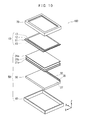
- FIG. 1 is an exploded perspective view schematically showing a configuration of a liquid crystal display device 100 according to an embodiment of the present invention.
- (A) is a top view of the LED board 32 which comprises the backlight 30 of embodiment of this invention.
- FIG. 4B is a diagram illustrating a lighting state of the LED element 35 on the LED substrate 32.
- 4 is a block diagram for explaining a configuration of a liquid crystal display device 100.
- FIG. 4 is a top view showing a configuration of a mother board 31 including a plurality of LED boards 32.
- FIG. 3 is a circuit diagram showing a configuration of a test pattern circuit 71 formed on an LED substrate 32.
- FIG. 3 is a circuit diagram showing a configuration of a test pattern circuit 71 formed on an LED substrate 32.
- FIG. (A) is a figure which shows the flow of the electric current at the time of making the test point 75 into conduction.
- (B) is a diagram showing a current flow when the test point 75 is disconnected.
- (A) is a figure which shows the state of conduction
- (b) is a figure which shows the lighting / non-lighting state of the LED element 35.
- FIG. 4 is an exploded perspective view schematically showing a configuration of a modified example of the liquid crystal display device 100.
- FIG. 4 is an exploded perspective view schematically showing a configuration of a modified example of the liquid crystal display device 100.
- FIG. 1 is an exploded perspective view schematically showing a configuration of a liquid crystal display device 100 according to an embodiment of the present invention.
- the liquid crystal display device 100 of the present embodiment is a liquid crystal display device capable of displaying an image.
- the liquid crystal display device 100 includes a liquid crystal panel 10 and a backlight unit 50 including a backlight 30 that irradiates the liquid crystal panel 10 with light.
- the liquid crystal panel 10 of the present embodiment generally has a rectangular shape as a whole, and is composed of a pair of translucent substrates (glass substrates) 11 and 12. Both the substrates 11 and 12 are arranged to face each other, and a liquid crystal layer (not shown) is provided between them.
- the liquid crystal layer is made of a liquid crystal material whose optical characteristics change with application of an electric field between the substrates 11 and 12.
- a sealing agent (not shown) is provided on the outer edge portions of the substrates 11 and 12 to seal the liquid crystal layer.
- polarizing plates 13 and 13 are attached to the outer surfaces of both the substrates 11 and 12, respectively.
- the back side of the substrates 11 and 12 is the array substrate (TFT substrate) 11, while the front side is the color filter substrate (CF substrate) 12.
- the liquid crystal panel 10 of the present embodiment has a size of, for example, 20 inches to 110 inches (typically 32 inches to 60 inches).
- the backlight unit 50 is a light source unit that irradiates the liquid crystal panel 10 with light.
- the backlight unit 50 of the present embodiment includes optical sheets 21a to 21c, a backlight 30, and a backlight chassis 40 that stores them.
- the backlight 30 in the example shown in FIG. 1 is a direct type LED backlight.
- the backlight 30 of the present embodiment includes a plurality of LED elements 35 and an LED substrate 32 on which the plurality of LED elements 35 are arranged. In the LED substrate 32 of the present embodiment, the plurality of LED elements 35 are arranged in an array. Each LED element 35 consists of a white LED chip, for example.
- a barcode 62 is formed on a part of the LED substrate 32.
- the bar code 62 is provided with information on the LED element 35 (for example, specifications such as LED type, model number, and brightness), board serial code, and manufacturing history.
- the barcode 62 of this embodiment is a two-dimensional barcode, and is produced by laser irradiation (laser marking) in the production process of the LED substrate 32.
- the backlight unit 50 of the present embodiment includes a backlight chassis 40 in which the backlight 30 composed of the LED substrate 32 is accommodated.
- the backlight chassis 40 of the present embodiment is made of a metal material (for example, aluminum, iron, etc.) and is a sheet metal member that covers the entire back surface of the liquid crystal display device 100.
- An optical sheet 21 (21a to 21c) is disposed between the backlight 30 and the liquid crystal panel 10.
- the optical sheets 21a to 21c are, for example, a lens sheet, a prism sheet, and a diffusion plate, respectively.
- the liquid crystal display device 100 of the present embodiment is provided with a bezel 55.
- the bezel 55 is a frame member that is made of a metal material (for example, aluminum or iron) and that fixes the outer edge portion of the liquid crystal panel 10 by pressing.
- the LED elements 35 arranged on the LED substrate 32 can display the same pattern as the pattern included in the barcode 62. Therefore, even if the barcode of the LED substrate 32 is hidden, the information on the barcode can be read by the display of the LED element 35 on the LED substrate 32. Subsequently, the description will be further continued with reference to FIG.
- FIG. 2A is a plan view of the LED substrate 32 constituting the backlight 30.
- LED elements 35 arranged in an array are formed on the LED substrate 32.
- a barcode region 60 in which a barcode 62 is formed is provided in a region of the LED substrate 32 where the LED elements are not disposed (a part of the outer peripheral region of the LED substrate). In this barcode area 60, laser marking is performed to form a two-dimensional barcode 62.
- FIG. 2B shows a state in which the LED element 35 on the LED substrate 32 is lit.
- a lighting state is represented by LED element 35a (shaded circle)
- a light extinction state is represented by LED element b (dotted white circle).
- the same pattern as the pattern included in the barcode 62 shown in FIG. 2A can be displayed on the LED element 35 (35a).
- the information of the two-dimensional barcode 62 is obtained by reading the light emission pattern of the LED element 35 (35a). It becomes possible to read.
- the light emission pattern by the LED element 35a may be the same as the entire pattern of the two-dimensional barcode 62. It may coincide with the pattern of the part.
- the light emission pattern by the LED element 35a is identified by, for example, an image recognition device, and the barcode information can be read by the image recognition device.
- the LED substrate 32 including the LED element 35 is imaged by an imaging device (for example, a CCD image sensor, a CMOS image sensor, etc.), and the imaging information is sent to the image recognition device.
- the light emission pattern of the LED element 35a is replaced with two-dimensional barcode information by an image analysis program stored in the image recognition apparatus, and the two-dimensional barcode information is replaced with predetermined necessary information (for example, an LED element).
- 35 information, serial code of the board 32, manufacturing history, etc.), and the predetermined necessary information can be displayed on an image display device (for example, a liquid crystal monitor).
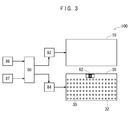
- FIG. 3 is a block diagram for explaining the configuration of the liquid crystal display device 100 of the present embodiment.
- the liquid crystal display device 100 of this embodiment includes a liquid crystal panel 10 and a backlight 30.
- the liquid crystal panel 10 and the backlight 30 are connected to a control device 80 that controls the operation of the liquid crystal display device 100.
- the control device 80 includes a semiconductor integrated circuit, and is, for example, an MPU (micro processor unit). Further, the control device 80 can be provided with a storage device (semiconductor memory, hard disk, optical disk, etc.), and various programs can be stored in the storage device, and various data and calculation results can be stored. It is.
- the control device 80 of the present embodiment includes a liquid crystal panel driving unit 82 and an LED driving unit 84.
- the liquid crystal panel driving unit 82 is a part that displays an image on the liquid crystal panel 10 by driving the liquid crystal panel 10.
- the liquid crystal panel driving unit 82 drives the liquid crystal panel 10 based on a signal input from the control device 80.
- the liquid crystal panel driving unit (liquid crystal panel driving device) 82 corresponds to a driver circuit such as a gate driver or a source driver.
- the LED drive unit 84 is a part for individually turning on / off each LED element 35 and changing the light emission intensity.
- the LED drive unit 84 can individually drive the LED elements 35 based on signals input from the control device 80.
- the LED drive unit (LED drive device) 84 is configured by a driver circuit (for example, an LED driver) including, for example, a switch.
- an external system 86 and an external power supply 87 can be separately connected to the control device 80.
- the external system 86 is a device for inputting image information to the control device 80.
- the external system 86 corresponds to, for example, a stand-alone personal computer (PC) or a PC connected to a network server that stores image information.
- the external power supply 87 is a power supply for supplying power to the liquid crystal display device 100 of the present embodiment, and corresponds to, for example, a commercial power supply.
- the LED driving unit 84 drives the LED element 35 when displaying the liquid crystal panel 10 and also drives the LED element 35 for displaying the pattern included in the two-dimensional barcode 62. be able to. Specifically, pattern information included in the barcode 62 is transmitted to the LED drive unit 84, and the LED drive unit 84 displays the light emission pattern of the LED element 35 based on the information.
- the pattern information may be stored in a storage device (not shown) connected to the LED drive unit 84.
- the storage device may be provided in the LED drive unit 84 or in the control device 80.
- FIG. 4 shows a configuration of a mother board (mother LED board) 31 including a plurality of LED boards 32.
- a bar code 62 is formed on each LED board 32.
- the LED element 35 of each LED board 32 can display the pattern contained in the barcode 62 of each LED board 32.
- the LED drive unit (for example, LED driver) 84 can cause the LED element 35 to display the pattern included in the barcode 62 with the light emission pattern, but is not limited thereto.
- a bar code display of the LED element 35 may be executed by forming a test pattern circuit for displaying a pattern included in the bar code on the LED substrate 32 and passing a current through the test pattern circuit.
- FIG. 5 is a circuit diagram showing a configuration of the test pattern circuit 71 formed on the LED substrate 32 of the present embodiment.
- the test pattern circuit 71 is connected to each LED element 35.
- the LED elements 35 (1-1), 35 (2-1),... Are arranged along the row direction, and the LED elements 35 (1-1), 35 (1-2) along the column direction. ), 35 (1-3), 35 (1-4)...
- the test pattern circuit 71 of the present embodiment is connected to a barcode pattern lighting power source (DC power source) 70.
- the test pattern circuit 71 includes a row line portion 71a extending in the row direction and a column line portion 71b extending in the column direction.
- An LED line portion 71c connected to the LED element 35 extends from the column line portion 71b.
- the LED line portion 71c extends to be connected to the ground after being connected to the LED element (light emitting diode) 35.
- a test point 75 that can be cut is formed in a part of the test pattern circuit 71 (specifically, the LED line portion 71c).
- the test point 75 can be cut by laser irradiation.
- no current flows through the LED element 35 so that the LED element 35 is not lit. Since this laser irradiation can be performed using a laser device for forming the barcode 62 on the LED substrate 32, there is an advantage that a new capital investment is not required.
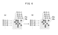
- FIG. 6A shows the state of conduction / disconnection of the test point 75 included in the test pattern circuit 71.
- FIG. 6B shows a state where the LED element 35 connected to the test pattern circuit 71 is turned on / off.
- test point 75 in a conductive state without being cut is represented by a test point 75a.
- test point 75 that has been cut and disconnected is represented by a test point 75b.
- the current from the barcode pattern lighting power source 70 does not flow through the LED element 35 connected to the test point 75b in the disconnected state.
- a display pattern is formed by the LED elements 35a connected to the test point 75a in a conductive state.
- the pattern included in the barcode can be displayed on the LED element 35a by cutting (breaking) the test point 75.
- the barcode pattern can be displayed by the LED element 35 without using a driver circuit (for example, an LED driver). Therefore, there is an advantage that the barcode pattern can be displayed by the LED element 35 even before the driver circuit (LED driver) is connected to the LED substrate 32.
- a driver circuit for example, an LED driver
- the LED element 35 connected to the test point 75 that has not been cut is configured to emit light, but conversely, as shown in FIG. It is also possible to configure the connected LED element 35 to emit light.
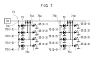
- FIG. 7 is a circuit diagram showing a configuration of the test pattern circuit 71 formed on the LED substrate 32 of the present embodiment.
- the test pattern circuit 71 is connected to each LED element 35.
- the test pattern circuit 71 is connected to a barcode pattern lighting power source (DC power source) 70.
- DC power source DC power source
- the test pattern circuit 71 includes a row line portion 71a extending in the row direction and a column line portion 71b extending in the column direction.
- An LED line portion 71c connected to the LED element 35 extends from the column line portion 71b.
- the LED line portion 71c extends to be connected to the ground after being connected to the NOT circuit (logic circuit) 73 and the LED element (light emitting diode) 35.
- the NOT circuit 73 is also connected to the ground (GND).
- connection line portion 71d extending from the row line portion 71a is connected.
- a test point 75 that can be cut is formed between the NOT circuit 73 and the column line portion 71b in the LED line portion 71c. The test point 75 can be cut by laser irradiation.
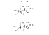
- FIG. 8A shows a case where the test point 75 of the test pattern circuit 71 shown in FIG. 7 is made conductive without being cut.
- FIG. 8B shows a case where the test point 75 of the test pattern circuit 71 is cut and disconnected.
- FIG. 9A shows the state of conduction / disconnection of the test point 75 included in the test pattern circuit 71.
- FIG. 9B shows a state in which the LED element 35 connected to the test pattern circuit 71 is lit (35a) / not lit (35b).
- a pattern is formed by light emission of the LED element 35a connected to the disconnected test point 75b. Can do.
- the test pattern circuit 71 shown in FIG. 7 also has an advantage that a bar code pattern can be displayed by the LED element 35 without using a driver circuit (for example, an LED driver).
- the LED substrate can be formed with a simple circuit configuration. 32 information can be read. That is, even if the barcode 62 is hidden, the information on the barcode 62 can be read by the display of the LED element 35. Further, it is possible to read barcode information without using a technique for attaching a wireless ID tag chip and antenna wiring. Therefore, it is not necessary to separately produce an ID tag function circuit including a wireless ID tag chip and an antenna on the LED substrate 32, so that the cost for producing such an ID tag function circuit on the LED substrate, and Thus, the problem of requiring work time for manufacturing the circuit can be avoided.
- the LED elements 35 are arranged two-dimensionally (in an array) on the LED substrate 32, but the number and arrangement form of the LED elements 35 are suitably suitable according to the finished liquid crystal display device 100. What is necessary is just to adopt. Further, if the two-dimensional barcode information can be read by the light emission of the LED elements 35, the arrangement of the LED elements 35 is not limited to a matrix shape in which rows and columns intersect at right angles, but is arranged in a staggered pattern. It may be the one that was made.
- FIG. 10 is an exploded perspective view showing a configuration of the liquid crystal display device 100 including the backlight 30 having a configuration in which the LED elements 35 are arranged in a row on the LED substrate 32.
- the backlight 30 shown in FIG. 10 is a so-called edge light type LED backlight.
- the liquid crystal display device 100 shown in FIG. 10 includes a liquid crystal panel 10, a backlight unit 50 including a backlight 30, and a bezel 70.
- the backlight unit 50 includes optical sheets 21a to 21c, a backlight 30, and a backlight chassis 40 that houses them.
- the illustrated backlight 30 includes an LED substrate 32 on which LED elements 35 are arranged in a row, and a light guide plate 37.
- the LED element 35 is arranged to face one of the side surfaces (light incident surface) of the light guide plate 37, and light emitted from the LED element 35 enters the light guide plate 37 from the light incident surface of the light guide plate 37.
- the light guide plate 37 is an optical member that irradiates light incident on the light incident surface in a planar shape from the light emitting surface (upper surface).
- the light guide plate 37 is made of, for example, an acrylic plate.
- a dot pattern (not shown) serving as a reflective layer is formed on the bottom surface of the light guide plate 37 of the present embodiment.
- a one-dimensional barcode is formed on the LED substrate 32, and a pattern included in the one-dimensional barcode can be displayed by light emission of the LED element 35. Therefore, for example, even if the barcode of the LED substrate 32 is hidden in the manufacturing stage, the barcode information can be read by the light emission pattern of the LED elements 35 on the LED substrate 32.
- the barcode light emission in the LED elements 35 arranged in a line can be performed by the test pattern circuit 71 including the driver circuit (for example, LED driver) and the test point 75.
- the present invention can also be applied to a mother board including a plurality of LED boards 32 in which the LED elements 35 are arranged in a line. That is, even if the barcode on the mother board is hidden on the mother board at the manufacturing stage, the information on the barcode can be read by the light emission pattern of the LED elements 35 on each LED board 32.
- the image display unit is configured by using one liquid crystal panel 10, but one image display unit (multi-display) is formed by combining a plurality of liquid crystal panels 10. It is also possible to configure.
- the liquid crystal display device 100 in which such a plurality of liquid crystal panels 10 are combined can be used for a large-screen digital signage (for example, a display device of 100 inches or more).
- the technology of the embodiment of the present invention can also be used in an LED display device that does not include a liquid crystal panel.
- the technology of the embodiment of the present invention can be applied to an LED display device that displays an image including characters or pictures by irradiating light.
- the LED display device according to the embodiment of the present invention includes a plurality of LED elements 35, an LED substrate 32 on which the plurality of LED elements 35 are arranged, and a barcode 62 formed on a part of the LED substrate 32. Yes.
- the plurality of LED elements 35 arranged on the LED substrate 32 can display the same pattern as the pattern included in the barcode 62. In the LED display device having such a configuration, even if the barcode 62 of the LED substrate 32 is hidden and cannot be seen, the information of the barcode 62 can be read by the pattern of the LED elements 35 arranged on the LED substrate 32. .
Landscapes
- Engineering & Computer Science (AREA)
- Microelectronics & Electronic Packaging (AREA)
- Liquid Crystal (AREA)
- Planar Illumination Modules (AREA)
Abstract
簡易な回路構成によってLED基板の情報を読み取ることができるバックライトを提供する。液晶パネル(10)に光を照射するバックライト(30)であって、複数のLED素子(35)と、複数のLED素子(35)が配列されたLED基板(32)と、前記LED基板(32)の一部に形成されたバーコード(62)とを備え、LED基板(32)に配列された複数のLED素子(35)は、バーコード(62)に含まれるパターンと同一のパターンを表示する、バックライト(30)である。
Description
本発明は、バックライトまたはバックライトを備えた液晶表示装置に関する。特に、発光ダイオード(LED)を光源として用いたバックライトおよびそれを備えた液晶表示装置に関する。
なお、本出願は2010年10月21日に出願された日本国特許出願2010-236227号に基づく優先権を主張しており、その出願の全内容は本明細書中に参照として組み入れられている。
なお、本出願は2010年10月21日に出願された日本国特許出願2010-236227号に基づく優先権を主張しており、その出願の全内容は本明細書中に参照として組み入れられている。
液晶表示装置は、一対の透光性基板の間に液晶が封止されてなる液晶パネルと、当該液晶パネルの背面側に配置されたバックライトとから構成されている。液晶表示装置では、バックライトから出射された光が液晶パネルの背面側から照射されることによって、液晶パネルに表示された画像が視認可能となる。
従来のバックライトは、発光素子(光源と呼ぶこともある。)として冷陰極蛍光管を用いたものが多かったが、近年は、発光素子として発光ダイオード(LED)を用いたバックライトも増えてきている(例えば、特許文献1など)。
LEDを用いたバックライト(LEDバックライト)には、液晶パネルの背面側に導光板を配置し、その導光板の端部に複数のLEDを配列させる導光板方式がある。また、液晶パネルの背面側の直下にLEDをアレイ状に配列した直下型のLEDバックライトもある。直下型のLEDバックライトは、導光板方式のものと比較して、光の利用効率が高いという利点があるとともに、エリア調光を容易に実行しやすいというメリットがある。
直下型のLEDバックライトには、LEDをアレイ状に配列したLED基板が用いられる。このLED基板を製造する際には、LEDの情報、基板のシリアルコード、製造履歴などの情報を持たせた二次元バーコードを、レーザマーキングによってLED基板に形成している。しかしながら、LED基板に反射シートを載せたり、LED基板が含まれたモジュールを組み立てると、この二次元バーコードの部分が隠れてしまい、その結果、二次元バーコードが読み取れなくなってしまうことがある。二次元バーコードが読み取れなくなると、二次元バーコードからLED基板の情報を得ることができなくなってしまうので、LEDバックライトまたは液晶表示装置の製造工程において不都合が発生する。
このような不都合を回避するために、特許文献2では、ディスプレイモジュールを覆う外装部材の内側に無線式のIDタグチップを実装し、この無線式のIDタグチップに接続するアンテナ配線を可撓性基板にする技術を開示している。この技術によれば、無線式のIDタグチップに記録された情報を無線で読み出すことが可能である。したがって、製造履歴を非破壊で容易に追跡することが可能となる。
しかしながら、特許文献2で開示された技術を、LEDバックライトのLED基板に適用しようとすれば、LED基板に、無線式のIDタグチップおよびアンテナを含むIDタグ機能の回路を別途作製する必要がある。そのようなIDタグ機能の回路をLED基板に作製することはコストアップに繋がるとともに、当該回路を作製するための作業時間が必要となってしまう。さらには、LED基板に当該回路を配置する場所を用意しなければならず、LED基板の設計において制約が増えてしまうという欠点がある。
本発明はかかる点に鑑みてなされたものであり、その主な目的は、簡易な回路構成によってLED基板の情報を読み取ることができるバックライトを提供することにある。
本発明に係るバックライトは、液晶パネルに光を照射するバックライトであり、複数のLED素子と、複数のLED素子が配列されたLED基板と、前記LED基板の一部に形成されたバーコードとを備え、前記LED基板に配列された前記複数のLED素子は、前記バーコードに含まれるパターンと同一のパターンを表示する。
ある好適な実施形態において、前記複数のLED素子は、前記LED基板にアレイ状に配列されており、前記バーコードは、二次元バーコードである。
ある好適な実施形態では、さらに、前記複数のLED素子を個別に点灯・消灯させるLED駆動装置を備え、前記LED駆動装置は、前記バーコードに含まれるパターンを記憶する記憶部に接続されており、かつ、前記複数のLED素子に前記パターンを点灯させるものである。
ある好適な実施形態において、前記LED基板には、前記バーコードに含まれるパターンを前記複数のLEDによって表示させるテストパターン回路が形成されている。
ある好適な実施形態において、前記テストパターン回路には、レーザ照射によって切断されるテストポイントが含まれている。
ある好適な実施形態では、前記テストポイントを切断した形態において、前記複数のLEDが、前記バーコードに含まれるパターンを表示する。
ある好適な実施形態において、前記複数のLED素子は、前記LED基板に直線状に配列されており、前記バーコードは、一次元バーコードである。
本発明に係る液晶表示装置は、上記のバックライトと、前記バックライトからの光が照射される液晶パネルとを備えた液晶表示装置である。
本発明に係るLED表示装置は、光を照射することによって文字または絵を含む画像を表示するLED表示装置であり、複数のLED素子と、複数のLED素子が配列されたLED基板と、前記LED基板の一部に形成されたバーコードとを備え、前記LED基板に配列された前記複数のLED素子は、前記バーコードに含まれるパターンと同一のパターンを表示する。
本発明に係るバックライトの製造方法は、複数のLED素子が配列されたLED基板を用意する工程(a)と、前記LED基板にバーコードを形成する工程(b)と、前記バーコードに含まれるパターンと同一のパターンを、前記複数のLED素子に表示させるパターン表示回路を形成する工程(c)とを含む。
ある好適な実施形態では、前記工程(c)における前記パターン表示回路は、前記複数のLED素子を個別に点灯・消灯させる回路を含む半導体集積回路装置である。
ある好適な実施形態では、前記工程(b)において、前記バーコードはレーザ照射によって前記LED基板に形成され、前記工程(c)における前記パターン表示回路は、レーザ照射によって切断されるテストポイントを含むテストパターン回路である。
ある好適な実施形態において、前記複数のLED素子は、前記LED基板にアレイ状に配列されており、前記工程(b)における前記バーコードは二次元バーコードである。
ある好適な実施形態において、前記複数のLED素子は、前記LED基板にアレイ状に配列されており、前記バーコードは、二次元バーコードである。
ある好適な実施形態では、さらに、前記複数のLED素子を個別に点灯・消灯させるLED駆動装置を備え、前記LED駆動装置は、前記バーコードに含まれるパターンを記憶する記憶部に接続されており、かつ、前記複数のLED素子に前記パターンを点灯させるものである。
ある好適な実施形態において、前記LED基板には、前記バーコードに含まれるパターンを前記複数のLEDによって表示させるテストパターン回路が形成されている。
ある好適な実施形態において、前記テストパターン回路には、レーザ照射によって切断されるテストポイントが含まれている。
ある好適な実施形態では、前記テストポイントを切断した形態において、前記複数のLEDが、前記バーコードに含まれるパターンを表示する。
ある好適な実施形態において、前記複数のLED素子は、前記LED基板に直線状に配列されており、前記バーコードは、一次元バーコードである。
本発明に係る液晶表示装置は、上記のバックライトと、前記バックライトからの光が照射される液晶パネルとを備えた液晶表示装置である。
本発明に係るLED表示装置は、光を照射することによって文字または絵を含む画像を表示するLED表示装置であり、複数のLED素子と、複数のLED素子が配列されたLED基板と、前記LED基板の一部に形成されたバーコードとを備え、前記LED基板に配列された前記複数のLED素子は、前記バーコードに含まれるパターンと同一のパターンを表示する。
本発明に係るバックライトの製造方法は、複数のLED素子が配列されたLED基板を用意する工程(a)と、前記LED基板にバーコードを形成する工程(b)と、前記バーコードに含まれるパターンと同一のパターンを、前記複数のLED素子に表示させるパターン表示回路を形成する工程(c)とを含む。
ある好適な実施形態では、前記工程(c)における前記パターン表示回路は、前記複数のLED素子を個別に点灯・消灯させる回路を含む半導体集積回路装置である。
ある好適な実施形態では、前記工程(b)において、前記バーコードはレーザ照射によって前記LED基板に形成され、前記工程(c)における前記パターン表示回路は、レーザ照射によって切断されるテストポイントを含むテストパターン回路である。
ある好適な実施形態において、前記複数のLED素子は、前記LED基板にアレイ状に配列されており、前記工程(b)における前記バーコードは二次元バーコードである。
本発明によれば、LED基板に配列された複数のLED素子が、LED基板の一部に形成されたバーコードに含まれるパターンと同一のパターンを表示するので、簡易な回路構成によってLED基板の情報を読み取ることができる。すなわち、LED基板の一部に形成されたバーコードが隠れたとしても、LED基板における複数のLED素子の表示によって、当該バーコードの情報を読み取ることが可能となる。また、LED基板における複数のLED素子によって、バーコードに含まれるパターンと同一のパターンを表示することができるので、無線式のIDタグチップおよびアンテナ配線を取り付ける技術を用いなくても、バーコードの情報を読み取ることが可能となる。
以下、図面を参照しながら、本発明の実施形態を説明する。以下の図面においては、説明の簡潔化のために、実質的に同一の機能を有する構成要素を同一の参照符号で示す。なお、本発明は以下の実施形態に限定されない。
図1は、本発明の実施形態に係る液晶表示装置100の構成を模式的に示す分解斜視図である。図1に示すように、本実施形態の液晶表示装置100は、画像を表示可能な液晶表示装置である。液晶表示装置100は、液晶パネル10と、液晶パネル10に光を照射するバックライト30を含むバックライトユニット50とから構成されている。
本実施形態の液晶パネル10は、概して、全体として矩形の形状を有しており、一対の透光性基板(ガラス基板)11および12から構成されている。両基板11および12は、互いに対向して配置され、その間には液晶層(不図示)が設けられている。液晶層は、基板11および12の間の電界印加に伴って光学特定が変化する液晶材料からなる。なお、基板11および12の外縁部には、シール剤(不図示)が設けられて、液晶層を封止している。また、両基板11および12の外面には、それぞれ、偏光板13、13が貼り付けられている。本実施形態では、基板11および12のうち、裏側がアレイ基板(TFT基板)11であり、一方、表側がカラーフィルタ基板(CF基板)12である。なお、本実施形態の液晶パネル10は、例えば、20インチから110インチ(典型的には、32インチから60インチ)のサイズを有している。
バックライトユニット50は、液晶パネル10に光を照射する光源ユニットである。本実施形態のバックライトユニット50は、光学シート21aから21cと、バックライト30と、それらを収納するバックライトシャーシ40とから構成されている。図1に示した例のバックライト30は、直下型のLEDバックライトである。本実施形態のバックライト30は、複数のLED素子35と、複数のLED素子35が配列されたLED基板32とから構成されている。本実施形態のLED基板32では、複数のLED素子35はアレイ状に配列されている。各LED素子35は、例えば白色LEDチップからなる。
LED基板32の一部には、バーコード62が形成されている。バーコード62には、LED素子35の情報(例えば、LEDの種類、型番、輝度などのスペック)、基板のシリアルコード、製造履歴などの情報を持たせている。本実施形態のバーコード62は、二次元バーコードであり、LED基板32の作製工程においてレーザ照射(レーザマーキング)によって作製される。
本実施形態のバックライトユニット50には、LED基板32から構成されたバックライト30が収納されるバックライトシャーシ40が含まれている。本実施形態のバックライトシャーシ40は、金属材料(例えば、アルミニウム、鉄など)から構成されており、液晶表示装置100の裏面全体を覆う板金部材である。また、バックライト30と液晶パネル10との間には、光学シート21(21aから21c)が配置されている。この例では、光学シート21aから21cは、それぞれ、例えば、レンズシート、プリズムシート、拡散板である。また、本実施形態の液晶表示装置100にはベゼル55が設けられている。ベゼル55は、金属材料(例えば、アルミニウム、鉄)からなり、液晶パネル10の外縁部を押させて固定するフレーム部材である。
本実施形態の構成においては、LED基板32に配列されたLED素子35は、バーコード62に含まれるパターンと同一のパターンを表示することができる。したがって、LED基板32のバーコードが隠れたとしても、LED基板32におけるLED素子35の表示によって、当該バーコードの情報を読み取ることが可能となる。続いて、図2を参照しながら、さらに説明を続ける。
図2(a)は、バックライト30を構成するLED基板32の平面図である。LED基板32には、アレイ状に配列されたLED素子35が形成されている。また、LED基板32のうち、LED素子が配置されない領域(LED基板の外周領域の一部)には、バーコード62が形成されるバーコード領域60が設けられている。このバーコード領域60において、レーザマーキングが施されて、二次元バーコード62が形成される。
図2(b)は、LED基板32におけるLED素子35が点灯した状態を示している。図2(b)では、点灯状態をLED素子35a(斜線した丸)で表し、消灯状態をLED素子b(点線の白丸)で表している。本実施形態の構成によれば、図2(a)に示したバーコード62に含まれるパターンと同一のパターンをLED素子35(35a)で表示することができる。
したがって、LED基板32を用いてモジュールを組み立てる際に、二次元バーコード62の部分が隠れてしまっても、LED素子35(35a)の発光パターンを読み取ることによって、二次元バーコード62の情報を読み取ることが可能となる。LED素子35aによる発光パターンは、二次元バーコード62の全体パターンと一致するものであってもよいし、二次元バーコード62に含まれる一部のパターンで情報を提供できるのであれば、その一部のパターンと一致するものであってもよい。
LED素子35aによる発光パターンは、例えば、画像認識装置によって識別され、その画像認識装置によってバーコード情報を読み取ることが可能である。具体的には、LED素子35を含むLED基板32を、撮像装置(例えば、CCDイメージセンサ、CMOSイメージセンサなど)によって撮像し、その撮像情報を画像認識装置に送る。そして、画像認識装置に格納されている画像解析プログラムによって、LED素子35aの発光パターンを二次元バーコード情報に置き換え、そして、その二次元バーコード情報を、所定の必要な情報(例えば、LED素子35の情報、基板32のシリアルコード、製造履歴などの情報)にして、その所定の必要な情報を画像表示装置(例えば、液晶モニターなど)に表示させることができる。
図3は、本実施形態の液晶表示装置100の構成を説明するためのブロック図である。図3に示すように、本実施形態の液晶表示装置100は、液晶パネル10と、バックライト30とから構成されている。液晶パネル10とバックライト30とは、液晶表示装置100の動作を制御する制御装置80に接続されている。制御装置80は、半導体集積回路からなり、例えば、MPU(マイクロ・プロセッサ・ユニット)である。また、制御装置80に、記憶装置(半導体メモリ、ハードディスク、光ディスクなど)を備えるようにすることができ、その記憶装置に、各種プログラムを格納したり、各種データ・演算結果を記憶させることが可能である。
本実施形態の制御装置80は、液晶パネル駆動部82と、LED駆動部84とを有している。液晶パネル駆動部82は、液晶パネル10を駆動させることによって液晶パネル10に画像を表示させる部位である。液晶パネル駆動部82は、制御装置80から入力される信号に基づいて液晶パネル10を駆動する。具体的には、液晶パネル駆動部(液晶パネル駆動装置)82は、ゲートドライバ、ソースドライバなどのドライバ回路に該当する。一方、LED駆動部84は、各LED素子35を個別に点灯/消灯させたり、発光強度を変更させるための部位である。LED駆動部84は、制御装置80から入力される信号に基づいてLED素子35を個別に駆動させることができる。具体的には、LED駆動部(LED駆動装置)84は、例えばスイッチ等を含むドライバ回路(例えば、LEDドライバ)によって構成されている。
なお、制御装置80には、外部システム86および外部電源87を別途接続することができる。外部システム86は、画像情報を制御装置80に入力するための装置である。外部システム86は、例えば、スタンドアローン型のパーソナル・コンピュータ(PC)、または、画像情報を蓄積するネットワークサーバに接続されたPCなどが該当する。また、外部電源87は、本実施形態の液晶表示装置100に電力を供給するための電源であり、例えば、商用電源などが該当する。
本実施形態の構成では、LED駆動部84によって、液晶パネル10を表示させる際におけるLED素子35の駆動とともに、二次元バーコード62に含まれるパターンを表示するためのLED素子35の駆動を実行することができる。具体的には、LED駆動部84に、バーコード62に含まれるパターンの情報を送信し、そして、その情報に基づいてLED駆動部84が、LED素子35の発光パターンを表示させるようにする。そのパターンの情報は、LED駆動部84に接続された記憶装置(不図示)に格納しておけばよい。その記憶装置は、LED駆動部84内に設けてもよいし、制御装置80内に設けてもよい。
図4は、複数のLED基板32を含むマザー基板(マザーLED基板)31の構成を示している。図4に示したマザー基板31では、各LED基板32にバーコード62が形成されている。そして、各LED基板32のLED素子35は、各LED基板32のバーコード62に含まれるパターンを表示することができる。したがって、製造段階のマザー基板31において、マザー基板31のバーコード62が隠れたとしても、各LED基板32におけるLED素子35の発光パターンによって、バーコード62の情報を読み取ることができる。
上述の実施形態の構成においては、LED駆動部(例えば、LEDドライバ)84によって、バーコード62に含まれるパターンをLED素子35が発光パターンによって表示させることができるが、これに限定されない。例えば、LED基板32に、バーコードに含まれるパターンを表示させるテストパターン回路を形成し、そのテストパターン回路に電流を流すことによって、LED素子35のバーコード表示を実行するようにしてもよい。
図5は、本実施形態のLED基板32に形成されるテストパターン回路71の構成を示す回路図である。テストパターン回路71は、各LED素子35に接続されている。LED素子35は、行方向に沿ってLED素子35(1-1)、35(2-1)・・が配列され、列方向に沿ってLED素子35(1-1)、35(1-2)、35(1-3)、35(1-4)・・が配列されている。
本実施形態のテストパターン回路71は、バーコードパターン点灯用電源(DC電源)70に接続されている。図示した例では、テストパターン回路71は、行方向に延びる行ライン部71aと、列方向に延びる列ライン部71bとを含んでいる。列ライン部71bからは、LED素子35に接続するLEDライン部71cが延びている。LEDライン部71cは、LED素子(発光ダイオード)35に接続された後、グランドに接続されるように延びている。
テストパターン回路71の一部(具体的には、LEDライン部71c)には、切断が可能なテストポイント75が形成されている。図5に示した構成例では、テストポイント75は、レーザ照射によって切断することが可能である。テストポイント75を切断して断線させると、LED素子35に電流が流れないので、そのLED素子35は不点灯状態になる。このレーザ照射は、LED基板32にバーコード62を形成する際のレーザ装置を用いて実行することが可能であるので、新たな設備投資が不要となるというメリットがある。
図6(a)は、テストパターン回路71に含まれるテストポイント75の導通・断線の状態を示している。一方、図6(b)は、テストパターン回路71に接続されたLED素子35の点灯・不点灯の状態を示している。
図6(a)においては、切断がなされず導通した状態のテストポイント75は、テストポイント75aで表している。一方、切断がされて断線した状態のテストポイント75は、テストポイント75bで表している。この例では、断線した状態のテストポイント75bに接続されたLED素子35には、バーコードパターン点灯用電源70からの電流が流れない。
したがって、図6(b)に示すように、導通した状態のテストポイント75aに接続されたLED素子35aによって表示パターンが形成される。このようにして、テストポイント75の切断(断線)によって、バーコードに含まれるパターンをLED素子35aで表示させることができる。
テストポイント75を含むテストパターン回路71によってLED素子35を表示させる手法によれば、ドライバ回路(例えば、LEDドライバ)を用いなくてもLED素子35によってバーコードのパターンを表示させることができる。したがって、LED基板32にドライバ回路(LEDドライバ)が接続される前の段階であっても、LED素子35でバーコードのパターンを表示することができるという利点がある。
図5に示したテストパターン回路71では、切断しなかったテストポイント75に接続されたLED素子35が発光するように構成したが、逆に、図7に示すように、切断したテストポイント75に接続されたLED素子35を発光するように構成することも可能である。
図7は、本実施形態のLED基板32に形成されるテストパターン回路71の構成を示す回路図である。テストパターン回路71は、各LED素子35に接続されている。また、テストパターン回路71は、バーコードパターン点灯用電源(DC電源)70に接続されている。
図示した例では、テストパターン回路71は、行方向に延びる行ライン部71aと、列方向に延びる列ライン部71bとを含んでいる。列ライン部71bからは、LED素子35に接続するLEDライン部71cが延びている。LEDライン部71cは、NOT回路(論理回路)73及びLED素子(発光ダイオード)35に接続された後、グランドに接続されるように延びている。なお、NOT回路73もグランド(GND)に接続されている。
LEDライン部71cのうちNOT回路73とLED素子35との間には、行ライン部71aから延びた接続ライン部71dが接続されている。そして、LEDライン部71cのうちNOT回路73と列ライン部71bとの間には、切断が可能なテストポイント75が形成されている。テストポイント75は、レーザ照射によって切断することが可能である。
ここで、図7に示したテストパターン回路71のテストポイント75を切断せずに導通させた場合を図8(a)に示す。一方、テストパターン回路71のテストポイント75を切断して断線させた場合を図8(b)に示す。
図8(a)に示すように、テストポイント75(75a)が導通している場合、NOT回路73の入力側が+になり、出力側がグランド(GND)に落ちるため、電流72bは、LED素子35bに流れない。一方、図8(b)に示すように、テストポイント75(75b)が断線している場合、NOT回路73の入力側が0になり、出力側とグランド(GND)とはつながらない。したがって、電流72aはLED素子35aに流れて、LED素子35aが発光する。すなわち、切断したテストポイント75bに接続されたLED素子35aによって表示パターンを形成することができる。
図9(a)は、テストパターン回路71に含まれるテストポイント75の導通・断線の状態を示している。一方、図9(b)は、テストパターン回路71に接続されたLED素子35の点灯(35a)・不点灯(35b)の状態を示している。図9(a)および(b)に示すように、図7に示したテストパターン回路71の構成においては、断線させたテストポイント75bに接続されたLED素子35aの発光によって、パターンを形成することができる。そして、図7に示したテストパターン回路71においても、ドライバ回路(例えば、LEDドライバ)を用いなくてもLED素子35によってバーコードのパターンを表示させることができるという利点がある。
本実施形態のバックライト30によれば、LED基板32に配列された複数のLED素子35がバーコード62に含まれるパターンと同一のパターンを表示することができるので、簡易な回路構成によってLED基板32の情報を読み取ることができる。すなわち、バーコード62が隠れたとしても、LED素子35の表示によって当該バーコード62の情報を読み取ることができる。また、無線式のIDタグチップおよびアンテナ配線を取り付ける技術を用いなくても、バーコードの情報を読み取ることが可能となる。したがって、LED基板32に、無線式のIDタグチップおよびアンテナを含むIDタグ機能の回路を別途作製する必要がないので、そのようなIDタグ機能の回路をLED基板に作製する場合のコストアップ、および、当該回路を作製するための作業時間が必要という問題を回避することができる。
上述した実施形態では、LED基板32にLED素子35を二次元的に(アレイ状に)配列させたが、LED素子35の個数および配列形式は、完成品の液晶表示装置100にあわせて適宜好適なものを採用すればよい。また、LED素子35の発光で二次元バーコード情報を読み取ることができるのであれば、LED素子35の配列は、行×列が直角に交わるマトリックス状のものに限らず、千鳥格子状に配列されたものであっても構わない。
加えて、LED素子35をLED基板32一列に配列させて、それによって、一次元バーコード情報を表示させるようにしても構わない。図10は、LED基板32にLED素子35が一列に配列された構成のバックライト30を含む液晶表示装置100の構成を示す分解斜視図である。図10に示したバックライト30は、所謂エッジライト型LEDバックライトである。
図10に示した液晶表示装置100は、液晶パネル10と、バックライト30を含むバックライトユニット50と、ベゼル70とから構成されている。バックライトユニット50は、光学シート21aから21cと、バックライト30と、それらを収納するバックライトシャーシ40とから構成されている。
図示したバックライト30は、LED素子35が一列に配列されたLED基板32と、導光板37とから構成されている。LED素子35は、導光板37の側面の一つ(入光面)に対向して配置されており、LED素子35から出射された光は、導光板37の入光面から導光板37内に入射する。導光板37は、入光面に入射した光を、発光面(上面)から面状に照射する光学部材である。導光板37は、例えば、アクリル板から構成されている。本実施形態の導光板37の底面には、反射層となるドットパターン(不図示)が形成されている。
図10に示した構成では、LED基板32に一次元バーコードを形成し、そして、その一次元バーコードに含まれるパターンをLED素子35の発光で表示することができる。したがって、例えば製造段階において、LED基板32のバーコードが隠れたとしても、LED基板32におけるLED素子35の発光パターンによって、バーコードの情報を読み取ることができる。一列に配列したLED素子35におけるバーコード用発光は、上述したように、ドライバ回路(例えば、LEDドライバ)、テストポイント75を含むテストパターン回路71によって行うことができる。加えて、LED素子35が一列に配列されたLED基板32を複数含むマザー基板においても適用することができる。すなわち、製造段階のマザー基板において、マザー基板のバーコードが隠れたとしても、各LED基板32におけるLED素子35の発光パターンによって、そのバーコードの情報を読み取ることができる。
以上、本発明を好適な実施形態により説明してきたが、こうした記述は限定事項ではなく、勿論、種々の改変が可能である。例えば、上述した実施形態の液晶表示装置100では、1枚の液晶パネル10を用いて画像表示部を構成しているが、複数枚の液晶パネル10を組み合わせて1つの画像表示部(マルチディスプレイ)を構成することも可能である。そのような複数枚の液晶パネル10を組み合わせた液晶表示装置100を、大画面のデジタルサイネージ(例えば、100インチ以上の表示装置)の用途に使用することも可能である。
さらには、液晶パネルを備えてないLED表示装置においても、本発明の実施形態の技術を用いることができる。具体的には、光を照射することによって文字または絵を含む画像を表示するLED表示装置に、本発明の実施形態の技術を適用することができる。本発明の実施形態に係るLED表示装置は、複数のLED素子35と、複数のLED素子35が配列されたLED基板32と、LED基板32の一部に形成されたバーコード62とを備えている。そして、LED基板32に配列された複数のLED素子35は、バーコード62に含まれるパターンと同一のパターンを表示することが可能である。このような構成を有するLED表示装置では、LED基板32のバーコード62が隠れて見えなくなっても、LED基板32に配列されたLED素子35によるパターンによって、バーコード62の情報を読み取ることができる。
本発明によれば、簡易な回路構成によってLED基板の情報を読み取ることができるバックライトを提供することができる。
10 液晶パネル
11 アレイ基板
12 CF基板
13 偏光板
21 光学シート
30 バックライト
31 マザー基板
32 LED基板
35 LED素子
37 導光板
40 バックライトシャーシ
50 バックライトユニット
60 バーコード領域
62 バーコード
70 バーコードパターン点灯用電源
71 テストパターン回路
71a 行ライン部
71b 列ライン部
71c LEDライン部
71d 接続ライン部
73 NOT回路(論理回路)
75 テストポイント
80 制御装置
82 液晶パネル駆動部
84 LED駆動部
86 外部システム
87 外部電源
100 液晶表示装置
11 アレイ基板
12 CF基板
13 偏光板
21 光学シート
30 バックライト
31 マザー基板
32 LED基板
35 LED素子
37 導光板
40 バックライトシャーシ
50 バックライトユニット
60 バーコード領域
62 バーコード
70 バーコードパターン点灯用電源
71 テストパターン回路
71a 行ライン部
71b 列ライン部
71c LEDライン部
71d 接続ライン部
73 NOT回路(論理回路)
75 テストポイント
80 制御装置
82 液晶パネル駆動部
84 LED駆動部
86 外部システム
87 外部電源
100 液晶表示装置
Claims (14)
- 液晶パネルに光を照射するバックライトであって、
複数のLED素子と、
複数のLED素子が配列されたLED基板と、
前記LED基板の一部に形成されたバーコードと
を備え、
前記LED基板に配列された前記複数のLED素子は、前記バーコードに含まれるパターンと同一のパターンを表示することを特徴とする、バックライト。 - 前記複数のLED素子は、前記LED基板にアレイ状に配列されており、
前記バーコードは、二次元バーコードであることを特徴とする、請求項1に記載のバックライト。 - さらに、前記複数のLED素子を個別に点灯・消灯させるLED駆動装置を備え、
前記LED駆動装置は、前記バーコードに含まれるパターンを記憶する記憶部に接続されており、かつ、前記複数のLED素子に前記パターンを点灯させることを特徴とする、請求項1または2に記載のバックライト。 - 前記LED基板には、前記バーコードに含まれるパターンを前記複数のLEDによって表示させるテストパターン回路が形成されている、請求項1または2に記載のバックライト。
- 前記テストパターン回路には、レーザ照射によって切断されるテストポイントが含まれている、請求項4に記載のバックライト。
- 前記テストポイントを切断した形態において、前記複数のLEDが、前記バーコードに含まれるパターンを表示することを特徴とする、請求項5に記載のバックライト。
- 前記複数のLED素子は、前記LED基板に直線状に配列されており、
前記バーコードは、一次元バーコードであることを特徴とする、請求項1に記載のバックライト。 - 請求項1から7の何れか一つに記載のバックライトと、
前記バックライトからの光が照射される液晶パネルと、
を備えた液晶表示装置。 - 光を照射することによって文字または絵を含む画像を表示するLED表示装置であって、
複数のLED素子と、
複数のLED素子が配列されたLED基板と、
前記LED基板の一部に形成されたバーコードと
を備え、
前記LED基板に配列された前記複数のLED素子は、前記バーコードに含まれるパターンと同一のパターンを表示することを特徴とする、LED表示装置。 - バックライトの製造方法であって、
複数のLED素子が配列されたLED基板を用意する工程(a)と、
前記LED基板にバーコードを形成する工程(b)と、
前記バーコードに含まれるパターンと同一のパターンを、前記複数のLED素子に表示させるパターン表示回路を形成する工程(c)と
を含む、バックライトの製造方法。 - 前記工程(c)における前記パターン表示回路は、前記複数のLED素子を個別に点灯・消灯させる回路を含む半導体集積回路装置である、請求項10に記載のバックライトの製造方法。
- 前記工程(b)において、前記バーコードはレーザ照射によって前記LED基板に形成され、
前記工程(c)における前記パターン表示回路は、レーザ照射によって切断されるテストポイントを含むテストパターン回路である、請求項10に記載のバックライトの製造方法。 - 前記工程(a)において、前記LED基板は、複数のLED基板を含むマザー基板の形態で用意される、請求項10から12の何れか一つに記載のバックライトの製造方法。
- 前記複数のLED素子は、前記LED基板にアレイ状に配列されており、
前記工程(b)における前記バーコードは二次元バーコードである、請求項10から13の何れか一つに記載のバックライトの製造方法。
Applications Claiming Priority (2)
| Application Number | Priority Date | Filing Date | Title |
|---|---|---|---|
| JP2010-236227 | 2010-10-21 | ||
| JP2010236227 | 2010-10-21 |
Publications (1)
| Publication Number | Publication Date |
|---|---|
| WO2012053468A1 true WO2012053468A1 (ja) | 2012-04-26 |
Family
ID=45975180
Family Applications (1)
| Application Number | Title | Priority Date | Filing Date |
|---|---|---|---|
| PCT/JP2011/073802 Ceased WO2012053468A1 (ja) | 2010-10-21 | 2011-10-17 | バックライトおよび液晶表示装置 |
Country Status (1)
| Country | Link |
|---|---|
| WO (1) | WO2012053468A1 (ja) |
Cited By (2)
| Publication number | Priority date | Publication date | Assignee | Title |
|---|---|---|---|---|
| FR3042847A1 (fr) * | 2015-10-23 | 2017-04-28 | Valeo Vision | Module lumineux pour un vehicule automobile a encodage bin electronique |
| JP2024049550A (ja) * | 2022-09-29 | 2024-04-10 | パナソニックIpマネジメント株式会社 | 防災用照明器具 |
Citations (4)
| Publication number | Priority date | Publication date | Assignee | Title |
|---|---|---|---|---|
| JPH02280287A (ja) * | 1989-04-21 | 1990-11-16 | Matsushita Electric Ind Co Ltd | バーコード信号発生装置 |
| JPH0320888A (ja) * | 1989-05-11 | 1991-01-29 | Seiko Epson Corp | バーコードキャラクタ表示装置 |
| JPH10173299A (ja) * | 1996-12-09 | 1998-06-26 | Calsonic Corp | プリント配線基板 |
| JP2009231380A (ja) * | 2008-03-19 | 2009-10-08 | Toyota Industries Corp | プリント配線板 |
-
2011
- 2011-10-17 WO PCT/JP2011/073802 patent/WO2012053468A1/ja not_active Ceased
Patent Citations (4)
| Publication number | Priority date | Publication date | Assignee | Title |
|---|---|---|---|---|
| JPH02280287A (ja) * | 1989-04-21 | 1990-11-16 | Matsushita Electric Ind Co Ltd | バーコード信号発生装置 |
| JPH0320888A (ja) * | 1989-05-11 | 1991-01-29 | Seiko Epson Corp | バーコードキャラクタ表示装置 |
| JPH10173299A (ja) * | 1996-12-09 | 1998-06-26 | Calsonic Corp | プリント配線基板 |
| JP2009231380A (ja) * | 2008-03-19 | 2009-10-08 | Toyota Industries Corp | プリント配線板 |
Cited By (2)
| Publication number | Priority date | Publication date | Assignee | Title |
|---|---|---|---|---|
| FR3042847A1 (fr) * | 2015-10-23 | 2017-04-28 | Valeo Vision | Module lumineux pour un vehicule automobile a encodage bin electronique |
| JP2024049550A (ja) * | 2022-09-29 | 2024-04-10 | パナソニックIpマネジメント株式会社 | 防災用照明器具 |
Similar Documents
| Publication | Publication Date | Title |
|---|---|---|
| JP4566958B2 (ja) | バックライトアセンブリ及びこれを利用した液晶表示装置モジュール | |
| KR102334862B1 (ko) | 백라이트 유닛 및 이를 포함하는 액정 표시 장치 | |
| KR101299130B1 (ko) | 액정표시장치 | |
| US9477124B2 (en) | Display device and television device | |
| JP2008235241A (ja) | バックライトアセンブリ及びそれを含む液晶表示装置 | |
| KR100999780B1 (ko) | 광학 어셈블리, 이를 구비한 백라이트 유닛 및 디스플레이 장치 | |
| JP2012018401A (ja) | 液晶表示装置 | |
| JP2010062456A (ja) | 光源、映像表示装置、および照明装置、ならびにそれらの製造方法 | |
| US20140375891A1 (en) | Display device, and television receiver device | |
| KR102133036B1 (ko) | 표시패널 및 이를 갖는 표시장치 | |
| KR101596791B1 (ko) | 백라이트 장치 및 이를 포함하는 디스플레이 장치 | |
| CN102767739A (zh) | 一种直下式激光背光模组及其显示器 | |
| KR20150074886A (ko) | 백라이트 유닛 및 이를 포함하는 액정 표시 장치 | |
| WO2010147062A1 (ja) | 表示装置 | |
| US9946010B2 (en) | Display device | |
| WO2012053468A1 (ja) | バックライトおよび液晶表示装置 | |
| US10754086B2 (en) | Display device with light source control | |
| JP2011096662A (ja) | Blu及びディスプレイ装置 | |
| JP5580566B2 (ja) | バックライトアセンブリ及びこれを含む液晶表示装置 | |
| KR20130010209A (ko) | 백라이트 유닛 및 표시 장치 | |
| JP5013524B2 (ja) | バックライトユニット及び液晶表示装置 | |
| US8698976B2 (en) | Light emitting device, illuminating apparatus having the same, and liquid crystal display apparatus | |
| KR20130001522A (ko) | 커버버툼 및 이를 포함하는 액정표시장치 | |
| CN112711156B (zh) | 显示面板的制造装置和制造方法 | |
| KR20130053568A (ko) | 백라이트 유닛 및 그를 이용한 디스플레이 장치 |
Legal Events
| Date | Code | Title | Description |
|---|---|---|---|
| 121 | Ep: the epo has been informed by wipo that ep was designated in this application |
Ref document number: 11834307 Country of ref document: EP Kind code of ref document: A1 |
|
| NENP | Non-entry into the national phase |
Ref country code: DE |
|
| 122 | Ep: pct application non-entry in european phase |
Ref document number: 11834307 Country of ref document: EP Kind code of ref document: A1 |
|
| NENP | Non-entry into the national phase |
Ref country code: JP |