WO2012053399A1 - 液晶表示装置 - Google Patents
液晶表示装置 Download PDFInfo
- Publication number
- WO2012053399A1 WO2012053399A1 PCT/JP2011/073367 JP2011073367W WO2012053399A1 WO 2012053399 A1 WO2012053399 A1 WO 2012053399A1 JP 2011073367 W JP2011073367 W JP 2011073367W WO 2012053399 A1 WO2012053399 A1 WO 2012053399A1
- Authority
- WO
- WIPO (PCT)
- Prior art keywords
- width
- data signal
- black matrix
- liquid crystal
- signal line
- Prior art date
- Legal status (The legal status is an assumption and is not a legal conclusion. Google has not performed a legal analysis and makes no representation as to the accuracy of the status listed.)
- Ceased
Links
Images



Classifications
-
- G—PHYSICS
- G02—OPTICS
- G02F—OPTICAL DEVICES OR ARRANGEMENTS FOR THE CONTROL OF LIGHT BY MODIFICATION OF THE OPTICAL PROPERTIES OF THE MEDIA OF THE ELEMENTS INVOLVED THEREIN; NON-LINEAR OPTICS; FREQUENCY-CHANGING OF LIGHT; OPTICAL LOGIC ELEMENTS; OPTICAL ANALOGUE/DIGITAL CONVERTERS
- G02F1/00—Devices or arrangements for the control of the intensity, colour, phase, polarisation or direction of light arriving from an independent light source, e.g. switching, gating or modulating; Non-linear optics
- G02F1/01—Devices or arrangements for the control of the intensity, colour, phase, polarisation or direction of light arriving from an independent light source, e.g. switching, gating or modulating; Non-linear optics for the control of the intensity, phase, polarisation or colour
- G02F1/13—Devices or arrangements for the control of the intensity, colour, phase, polarisation or direction of light arriving from an independent light source, e.g. switching, gating or modulating; Non-linear optics for the control of the intensity, phase, polarisation or colour based on liquid crystals, e.g. single liquid crystal display cells
- G02F1/133—Constructional arrangements; Operation of liquid crystal cells; Circuit arrangements
- G02F1/1333—Constructional arrangements; Manufacturing methods
- G02F1/1335—Structural association of cells with optical devices, e.g. polarisers or reflectors
- G02F1/133509—Filters, e.g. light shielding masks
- G02F1/133512—Light shielding layers, e.g. black matrix
-
- G—PHYSICS
- G02—OPTICS
- G02F—OPTICAL DEVICES OR ARRANGEMENTS FOR THE CONTROL OF LIGHT BY MODIFICATION OF THE OPTICAL PROPERTIES OF THE MEDIA OF THE ELEMENTS INVOLVED THEREIN; NON-LINEAR OPTICS; FREQUENCY-CHANGING OF LIGHT; OPTICAL LOGIC ELEMENTS; OPTICAL ANALOGUE/DIGITAL CONVERTERS
- G02F1/00—Devices or arrangements for the control of the intensity, colour, phase, polarisation or direction of light arriving from an independent light source, e.g. switching, gating or modulating; Non-linear optics
- G02F1/01—Devices or arrangements for the control of the intensity, colour, phase, polarisation or direction of light arriving from an independent light source, e.g. switching, gating or modulating; Non-linear optics for the control of the intensity, phase, polarisation or colour
- G02F1/13—Devices or arrangements for the control of the intensity, colour, phase, polarisation or direction of light arriving from an independent light source, e.g. switching, gating or modulating; Non-linear optics for the control of the intensity, phase, polarisation or colour based on liquid crystals, e.g. single liquid crystal display cells
- G02F1/133—Constructional arrangements; Operation of liquid crystal cells; Circuit arrangements
- G02F1/136—Liquid crystal cells structurally associated with a semi-conducting layer or substrate, e.g. cells forming part of an integrated circuit
- G02F1/1362—Active matrix addressed cells
Definitions
- the present invention relates to a display device, and more particularly to a liquid crystal display device formed by bonding two substrates together.
- the liquid crystal panel is formed by bonding two substrates and filling a liquid crystal substance between the substrates.
- a thin film transistor hereinafter referred to as TFT
- a counter electrode is formed on the other substrate, and a color filter including a black matrix is provided.
- TFT substrate the former is called a TFT substrate, and the latter is called a counter substrate.
- pixel circuits adjacent in the arrangement direction of data signal lines correspond to different colors and are associated with filter elements of different colors.
- a black matrix is provided between adjacent filter elements.
- the TFT substrate and the counter substrate are bonded so that the data signal line and the black matrix overlap each other.
- Patent Document 1 describes that the width of the black matrix is set to be equal to or smaller than the width of the data signal line in order to prevent display unevenness due to an abnormal shape or misalignment of the black matrix.
- Patent Document 2 describes that the width of the black matrix is 10 ⁇ m or more.
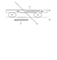
- the position of the data signal line and the black matrix shifts when viewed from an oblique direction, so that colors are mixed between adjacent pixels and color unevenness may occur (see FIG. 9).
- the TFT of the pixel circuit corresponding to the color Ca is turned off, and the TFT of the pixel circuit corresponding to the color Cb is turned on.
- the color Cb is seen by the observer seen from the front, but the color Ca appears to be mixed with the color Cb to the observer seen from the arrow direction.
- color unevenness hereinafter referred to as perspective color unevenness
- the width of the black matrix may be widened.
- the width of the black matrix is widened, another problem arises that the aperture ratio decreases and the display image becomes dark.
- the width of the black matrix or the data signal line is narrowed in order to increase the aperture ratio, the contrast and the uneven color of the perspective color become problems.
- an object of the present invention is to provide a liquid crystal display device excellent in aperture ratio, contrast, and color reproducibility.
- a first aspect of the present invention is a liquid crystal display device formed by bonding two substrates together, A first substrate including a plurality of pixel circuits arranged two-dimensionally and a plurality of data signal lines arranged parallel to each other; A plurality of filter elements corresponding to the pixel circuit, and a second substrate including a black matrix provided between adjacent filter elements in the arrangement direction of the data signal lines, The first and second substrates are bonded so that the black matrix covers the data signal lines, The width of the black matrix is 7 ⁇ m or less, the width of the black matrix is 1 ⁇ m or more wider than one side of the data signal line, and the sum of the width of the black matrix and the width of the data signal line is 9 ⁇ m or more. It is characterized by.
- the first and second substrates are bonded so that a central axis of the black matrix and a central axis of the data signal line overlap each other.
- the aperture ratio can be increased by setting the width of the black matrix to 7 ⁇ m or less.
- the contrast can be increased.
- the color reproducibility can be improved. Therefore, a liquid crystal display device excellent in aperture ratio, contrast, and color reproducibility can be provided.
- the second aspect of the present invention it is possible to minimize the decrease in the aperture ratio even when a deviation occurs when the substrates are bonded together.
- FIG. 4 is a cross-sectional view taken along line V-V ′ of FIG. 3. It is a figure which shows the range which satisfy
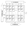
- FIG. 1 is a block diagram showing a configuration of a liquid crystal panel according to an embodiment of the present invention.
- the liquid crystal panel 1 shown in FIG. 1 is formed by bonding a TFT substrate 10 and a counter substrate 20 and filling a liquid crystal substance (not shown) between the substrates.
- m and n are integers of 2 or more
- i is an integer of 1 to m
- j is an integer of 1 to n.
- the scanning signal lines G1 to Gm are arranged in parallel to each other, and the data signal lines S1 to Sn are arranged in parallel to each other so as to be orthogonal to the scanning signal lines G1 to Gm.
- the pixel circuit Pij includes the TFT 11 and the pixel electrode 12, and is two-dimensionally arranged corresponding to the intersection of the scanning signal line Gi and the data signal line Sj.
- the gate terminal, the source terminal, and the drain terminal of the TFT 11 are connected to the scanning signal line Gi, the data signal line Sj, and the pixel electrode 12, respectively.
- the scanning signal lines are also called gate bus lines or gate lines
- the data signal lines are also called source bus lines or source lines.
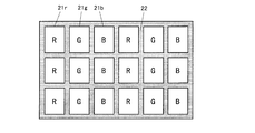
- FIG. 2 is a diagram illustrating a configuration of a color filter provided on the counter substrate 20.
- the color filter has a plurality of filter elements 21 corresponding to the pixel circuit Pij.
- the three pixel circuits Pij arranged in the arrangement direction of the data signal lines S1 to Sn (extending direction of the scanning signal lines G1 to Gm, the horizontal direction in the figure) include filter elements 21r and 21g corresponding to red, green and blue. , 21b are associated with each other.
- a black matrix 22 is provided between adjacent filter elements 21.
- the black matrix 22 is formed between the adjacent filter elements 21 in the direction in which the scanning signal lines G1 to Gm are arranged (the extending direction of the data signal lines S1 to Sn, the vertical direction in the figure) and in the direction in which the data signal lines S1 to Sn are arranged. It is provided between adjacent filter elements 21.
- the liquid crystal panel 1 is driven using a scanning signal line drive circuit 2, a data signal line drive circuit 3, and a counter electrode drive circuit 4.
- the scanning signal line driving circuit 2 sequentially selects one scanning signal line from the scanning signal lines G1 to Gm, and applies a potential at which the TFT 11 is turned on to the selected scanning signal line.
- the data signal line driving circuit 3 applies a potential corresponding to the video signal to the data signal lines S1 to Sn.
- the counter electrode drive circuit 4 fixedly applies a predetermined potential to the counter electrode, or alternately applies a relatively high potential and a relatively low potential. Note that all or part of these drive circuits may be integrally formed on the liquid crystal panel 1.
- FIG. 3 is a plan view of the liquid crystal panel 1.
- FIG. 3 shows a layout of the TFT substrate 10 and an arrangement position (indicated by a thick line) of the filter element 21.
- FIG. 3 there is a black matrix 22 other than the arrangement position of the filter element 21.
- description will be made by paying attention to the black matrix 22 provided between the filter elements 21 adjacent in the arrangement direction of the data signal lines S1 to Sn.
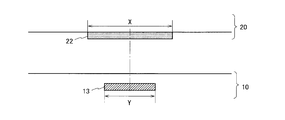
- FIG. 4 is a cross-sectional view taken along the line V-V ′ of FIG.
- FIG. 4 shows the data signal line 13 formed on the TFT substrate 10 and the black matrix 22 provided on the counter substrate 20.
- the black matrix 22 covers the data signal lines 13.
- the width of the black matrix 22 is denoted by X
- the width of the data signal line 13 is denoted by Y
- the sum of the two widths (X + Y) is denoted by A.
- (XY) / 2 is referred to as a one-side protruding amount and is represented as B.
- the liquid crystal panel of the present invention satisfies the following three conditions. (1) The width of the black matrix is 7 ⁇ m or less. (2) The width of the black matrix is 1 ⁇ m or more wider on one side than the width of the data signal line. (3) The sum of the width of the black matrix and the width of the data signal line is 9 ⁇ m or more.
- Example 1 As an example of (X, Y) that satisfies the above three conditions, the case of (5.5 ⁇ m, 3.5 ⁇ m) is the case of Example 1, the case of (6 ⁇ m, 3 ⁇ m) is the case of Example 2, and the case of (7 ⁇ m, 4 ⁇ m) This is referred to as Example 3.
- Example 3 In FIG. 5, Examples 1 to 3 correspond to point P, point S, and point T, respectively.
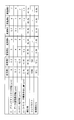
- FIG. 6 is a diagram showing two widths and performances of the conventional and the liquid crystal panels of the present invention.
- the width X of the black matrix, the width Y of the data signal lines, the sum A of the widths, the one-side protrusion amount B, the aperture ratio, the contrast, and the unevenness of the perspective color are measured or evaluated for seven types of liquid crystal panels. Results are listed.
- the aperture ratio depends on the structure of the base, it is necessary to align the pixel pitch when comparing the aperture ratios.
- the aperture ratio shown in FIG. 6 is calculated by aligning with the pixel pitch of Example 2 (the pixel pitch in the arrangement direction of the data signal lines is 25.5 ⁇ m and the pixel pitch in the arrangement direction of the scanning signal lines is 76.5 ⁇ m). It is.
- Conventional example 1 has a black matrix width of 8 ⁇ m
- conventional example 2 has a data signal line width of 7.2 ⁇ m.
- the aperture ratio is low.
- the width of the data signal line (7.2 ⁇ m) is wider than the width of the black matrix (5.3 ⁇ m). For this reason, in Conventional Example 2, part of the light scattered at the end of the data signal line is emitted to the front without being blocked by the black matrix, so that the luminance during black display increases and the contrast decreases.
- the aperture ratio is the highest, and uneven color of the perspective color does not occur.
- the conventional example 3 has a lower contrast than the other examples.
- the aperture ratio is the highest, and the contrast is higher than that in the conventional example 3, but uneven color of the perspective color occurs.
- the aperture ratio, contrast, and color reproducibility cannot all be improved at the same time.
- Example 1 the width of the black matrix is 5.5 ⁇ m, and the width of the data signal line is 3.5 ⁇ m.
- the aperture ratio is the highest among (X, Y) satisfying the above three conditions. Further, in Example 1, the contrast is high (see the description of FIG. 7), and the perspective color unevenness does not occur. Therefore, according to Example 1, contrast and color reproducibility can be improved while sufficiently increasing the aperture ratio.
- Example 2 the width of the black matrix is 6 ⁇ m, and the width of the data signal line is 3 ⁇ m.
- the one-side protrusion amount T is as large as 1.5 ⁇ m. For this reason, even if a deviation occurs when the substrates are bonded together, the light scattered at the end of the data signal line is easily blocked by the black matrix. Therefore, according to the second embodiment, the aperture ratio is lower than that of the first embodiment, but the contrast can be made higher than that of the first embodiment.
- Example 3 the width of the black matrix is 7 ⁇ m, and the width of the data signal line is 4 ⁇ m.
- the one-side protrusion amount T is the same as that in the second embodiment, and the width of the data signal line is wider than that in the second embodiment. Therefore, according to the third embodiment, it is possible to increase the width of the data signal line as compared with the second embodiment while increasing the same level of contrast as the second embodiment. In a high-definition liquid crystal panel, since the charging time of the data signal line is short, it is necessary to increase the width of the data signal line and reduce the load on the data signal line.
- Example 3 is suitable for such a case, for example.
- Example 3 when the width of the data signal line is increased from 3 ⁇ m to 4 ⁇ m with priority given to contrast, the width of the black matrix is increased from 6 ⁇ m to 7 ⁇ m.
- the width of the data signal line may be increased from 3 ⁇ m to 4 ⁇ m by giving priority to the aperture ratio, or the width of the black matrix may be kept at 6 ⁇ m.
- the width of the black matrix is less than 5 ⁇ m, the variation in line width becomes large and the characteristics become unstable. Accordingly, the width of the black matrix is at least 5 ⁇ m. If only the aperture ratio needs to be increased, the width of the black matrix may be 5 ⁇ m and the width of the data signal line may be 5 ⁇ m or less. However, such a liquid crystal panel has a problem in contrast or color reproducibility. Further, even if the width of the black matrix is made larger than 7 ⁇ m, the contrast is not so high, but the aperture ratio is lowered, so that the overall performance is lowered. Therefore, in the liquid crystal panel of the present invention, a margin of 2 ⁇ m is added to the minimum value of 5 ⁇ m so that the width of the black matrix is 7 ⁇ m or less.
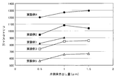
- FIG. 7 is a diagram showing the relationship between the one-side protrusion amount and the contrast.
- FIG. 7 shows the results of measuring the contrast when the width of the black signal is fixed and the width of the data signal line is changed for five types of liquid crystal panels.
- the horizontal axis represents the one-side protrusion amount B, and the vertical axis represents the contrast ratio.
- the contrast ratio is a value obtained by dividing the luminance measured in the front during white display by the luminance measured in the front during black display. In FIG. 6 and FIG. 7, the configuration of the liquid crystal panel to be measured is different.
- the protruding amount on one side is 1 ⁇ m or more. Therefore, in the liquid crystal panel of the present invention, the width of the black matrix is made 1 ⁇ m or more wider on one side than the width of the data signal line.
- the amount of deviation at the time of substrate bonding is about 3 ⁇ m at maximum.
- the distance between the black matrix and the data signal line is about 5 ⁇ m, and the refractive index of the insulating layer and the liquid crystal between the black matrix and the data signal line is about 1.5. It is.
- a deviation of 3 ⁇ m occurs when the substrates are bonded together, the amount of overlap between the black matrix and the data signal line when viewed from the front is 1 ⁇ m.
- a gap is seen between the black matrix and the data signal lines.
- the size of the gap is 1 ⁇ m. If there is a gap of 1 ⁇ m or more, the observer recognizes uneven color. Therefore, in this liquid crystal panel, color unevenness is recognized when viewed from a direction inclined by 33 ° or more from the front.
- a deviation of 3 ⁇ m occurs when the substrates are bonded together, the amount of overlap between the black matrix and the data signal line when viewed from the front is 1.5 ⁇ m.
- this liquid crystal panel is viewed from a direction inclined by 26 ° or more from the front, a gap can be seen between the black matrix and the data signal lines.
- the size of the gap is 1 ⁇ m. Therefore, in this liquid crystal panel, color unevenness is recognized when viewed from a direction inclined by 40 ° or more from the front.
- a range within about 30 ° from the front is a standard observation direction.
- the color reproducibility is good because the color unevenness is recognized only when it greatly exceeds the standard observation direction. Therefore, in the liquid crystal panel of the present invention, the sum of the width of the black matrix and the width of the data signal line is set to 9 ⁇ m or more.
- the aperture ratio can be increased by setting the width of the black matrix to 7 ⁇ m or less.
- the contrast can be increased by making the width of the black matrix wider by 1 ⁇ m or more per side than the width of the data signal line.
- the color reproducibility can be improved by setting the sum of the width of the black matrix and the width of the data signal line to 9 ⁇ m or more.
- the liquid crystal panel 1 (liquid crystal display device) of the present invention is formed by bonding two substrates together and arranged in parallel with each other, with a plurality of pixel circuits Pij arranged two-dimensionally.
- a TFT substrate 10 (first substrate) including a plurality of data signal lines S1 to Sn, a plurality of filter elements 21 corresponding to the pixel circuit Pij, and a filter element 21 adjacent in the arrangement direction of the data signal lines S1 to Sn.
- a counter substrate 20 (second substrate) including a black matrix 22 provided therebetween. The TFT substrate 10 and the counter substrate 20 are bonded together so that the black matrix 22 covers the data signal lines 13.
- the width of the black matrix 22 is 7 ⁇ m or less, and the width of the black matrix 22 is 1 ⁇ m per side of the width of the data signal line 13.
- the sum of the width of the black matrix 22 and the width of the data signal line 13 is 9 ⁇ m or more.
- liquid crystal display device of the present invention has the characteristics of excellent aperture ratio, contrast, and color reproducibility, it can be used for display devices of various electronic devices.
- SYMBOLS 1 Liquid crystal panel 2 ... Scanning signal line drive circuit 3 ... Data signal line drive circuit 4 ... Counter electrode drive circuit 10 ... TFT substrate 11 . TFT DESCRIPTION OF SYMBOLS 12 ... Pixel electrode 13, S1-Sn ... Data signal line 20 ... Opposite substrate 21 ... Filter element 22 ... Black matrix G1-Gm ... Scanning signal line Pij ... Pixel circuit
Landscapes
- Physics & Mathematics (AREA)
- Nonlinear Science (AREA)
- Mathematical Physics (AREA)
- Chemical & Material Sciences (AREA)
- Crystallography & Structural Chemistry (AREA)
- General Physics & Mathematics (AREA)
- Optics & Photonics (AREA)
- Liquid Crystal (AREA)
- Engineering & Computer Science (AREA)
- Microelectronics & Electronic Packaging (AREA)
- Devices For Indicating Variable Information By Combining Individual Elements (AREA)
Abstract
TFT基板10と対向基板20を貼り合わせるときに、対向基板20に設けられたブラックマトリクス22がTFT基板10に形成されたデータ信号線13を覆うようにする。ブラックマトリクスの幅を7μm以下とし、ブラックマトリクスの幅をデータ信号線の幅より片側につき1μm以上広くし、かつ、ブラックマトリクスの幅とデータ信号線の幅の和を9μm以上とする。これにより、開口率、コントラストおよび色再現性に優れた液晶表示装置を提供することができる。
Description
本発明は、表示装置に関し、特に、2枚の基板を貼り合わせて形成された液晶表示装置に関する。
液晶パネルは、2枚の基板を貼り合わせ、基板間に液晶物質を充填することにより形成される。一方の基板には、薄膜トランジスタ(Thin Film Transistor:以下、TFTと略称する)と画素電極を含む画素回路、走査信号線、および、データ信号線などが形成される。他方の基板には、対向電極が形成され、ブラックマトリクスを含むカラーフィルタが設けられる。以下、前者をTFT基板、後者を対向基板という。
一般的な液晶パネルでは、データ信号線の並び方向に隣接する画素回路は、異なる色に対応し、異なる色のフィルタ要素に対応づけられる。また、色再現性を良くするために、隣接するフィルタ要素間にはブラックマトリクスが設けられる。また、開口率を高くするために、TFT基板と対向基板は、データ信号線とブラックマトリクスが重なるように貼り合わされる。
本願発明に関して、特許文献1には、ブラックマトリクスの形状異常や配置ずれに起因する表示むらを防止するために、ブラックマトリクスの幅をデータ信号線の幅以下にすることが記載されている。特許文献2には、ブラックマトリクスの幅を10μm以上にすることが記載されている。
TFT基板と対向基板を貼り合わせるときには、最大で数μmのずれが発生する。このずれが発生すると、データ信号線の端で光が散乱し、液晶パネルのコントラストが低下する(図8を参照)。図8に示すように、TFT基板80と対向基板90を貼り合わせて形成された液晶パネルでは、データ信号線81の端で散乱した光Lの一部はブラックマトリクス91で遮られ、残りはブラックマトリクス91で遮られることなく正面に出射される。ところが、基板貼り合わせ時のずれ(図8に示すd)が大きくなると、正面に出射される光の量が多くなる。このため、黒表示のときの輝度が高くなり、液晶パネルのコントラストが低下する。
また、液晶パネルでは、斜めから見たときにデータ信号線とブラックマトリクスの位置がずれるので、隣接する画素間で色が混ざり、色むらが発生することがある(図9を参照)。図9に示す液晶パネルにおいて色Cbを表示する場合、色Caに対応した画素回路のTFTはオフ状態となり、色Cbに対応した画素回路のTFTはオン状態となる。正面から見た観測者には色Cbが見えるが、矢印方向から見た観測者には色Cbに色Caが混ざって見える。このように液晶パネルでは、斜めから見たときに色むら(以下、斜視色むらという)が発生し、色再現性が低下する。
コントラストと斜視色むらの問題を解決するためには、特許文献2に記載されたように、ブラックマトリクスの幅を広くすればよい。しかし、ブラックマトリクスの幅を広くすると、開口率が低下し、表示画像が暗くなるという別の問題が発生する。一方、開口率を高くするために、ブラックマトリクスやデータ信号線の幅を狭くすると、コントラストと斜視色むらが問題となる。
それ故に、本発明は、開口率とコントラストと色再現性に優れた液晶表示装置を提供することを目的とする。
本発明の第1の局面は、2枚の基板を貼り合わせて形成された液晶表示装置であって、
2次元状に配置された複数の画素回路、および、互いに平行に配置された複数のデータ信号線を含む第1基板と、
前記画素回路に対応する複数のフィルタ要素、および、前記データ信号線の並び方向に隣接するフィルタ要素間に設けられたブラックマトリクスを含む第2基板とを備え、
前記第1および第2基板は、前記ブラックマトリクスが前記データ信号線を覆うように貼り合わされ、
前記ブラックマトリクスの幅が7μm以下、前記ブラックマトリクスの幅が前記データ信号線の幅より片側につき1μm以上広く、かつ、前記ブラックマトリクスの幅と前記データ信号線の幅の和が9μm以上であることを特徴とする。
2次元状に配置された複数の画素回路、および、互いに平行に配置された複数のデータ信号線を含む第1基板と、
前記画素回路に対応する複数のフィルタ要素、および、前記データ信号線の並び方向に隣接するフィルタ要素間に設けられたブラックマトリクスを含む第2基板とを備え、
前記第1および第2基板は、前記ブラックマトリクスが前記データ信号線を覆うように貼り合わされ、
前記ブラックマトリクスの幅が7μm以下、前記ブラックマトリクスの幅が前記データ信号線の幅より片側につき1μm以上広く、かつ、前記ブラックマトリクスの幅と前記データ信号線の幅の和が9μm以上であることを特徴とする。
本発明の第2の局面は、本発明の第1の局面において、
前記第1および第2基板は、前記ブラックマトリクスの中心軸と前記データ信号線の中心軸が重なるように貼り合わされることを特徴とする。
前記第1および第2基板は、前記ブラックマトリクスの中心軸と前記データ信号線の中心軸が重なるように貼り合わされることを特徴とする。
本発明の第1の局面によれば、ブラックマトリクスの幅を7μm以下にすることにより、開口率を高くすることができる。ブラックマトリクスの幅をデータ信号線の幅より片側につき1μm以上広くすることにより、コントラストを高くすることができる。ブラックマトリクスの幅とデータ信号線の幅の和を9μm以上にすることにより、色再現性を良くすることができる。したがって、開口率、コントラストおよび色再現性に優れた液晶表示装置を提供することができる。
本発明の第2の局面によれば、基板貼り合わせ時にずれが発生したときでも、開口率の低下を最小限に留めることができる。
図1は、本発明の実施形態に係る液晶パネルの構成を示すブロック図である。図1に示す液晶パネル1は、TFT基板10と対向基板20を貼り合わせ、基板間に液晶物質(図示せず)を充填することにより形成される。以下、mおよびnは2以上の整数、iは1以上m以下の整数、jは1以上n以下の整数であるとする。
TFT基板10には、m本の走査信号線G1~Gm、n本のデータ信号線S1~Sn、および、(m×n)個の画素回路Pijが形成される。走査信号線G1~Gmは互いに平行に配置され、データ信号線S1~Snは走査信号線G1~Gmと直交するように互いに平行に配置される。画素回路Pijは、TFT11と画素電極12を含み、走査信号線Giとデータ信号線Sjの交点に対応して2次元状に配置される。TFT11のゲート端子、ソース端子およびドレイン端子は、それぞれ、走査信号線Gi、データ信号線Sjおよび画素電極12に接続される。なお、走査信号線はゲートバスラインあるいはゲート線とも呼ばれ、データ信号線はソースバスラインあるいはソース線とも呼ばれる。
対向基板20には、対向電極(図示せず)が形成され、カラーフィルタが設けられる。図2は、対向基板20に設けられるカラーフィルタの構成を示す図である。図2に示すように、カラーフィルタは、画素回路Pijに対応する複数のフィルタ要素21を有する。データ信号線S1~Snの並び方向(走査信号線G1~Gmの伸延方向。図では横方向)に並んだ3個の画素回路Pijには、赤、緑および青に対応したフィルタ要素21r、21g、21bがそれぞれ対応づけられる。隣接するフィルタ要素21の間には、ブラックマトリクス22が設けられる。ブラックマトリクス22は、走査信号線G1~Gmの並び方向(データ信号線S1~Snの伸延方向。図では縦方向)に隣接するフィルタ要素21の間と、データ信号線S1~Snの並び方向に隣接するフィルタ要素21の間とに設けられる。
液晶パネル1は、走査信号線駆動回路2、データ信号線駆動回路3、および、対向電極駆動回路4を用いて駆動される。走査信号線駆動回路2は、走査信号線G1~Gmの中から1本の走査信号線を順に選択し、選択した走査信号線に対してTFT11がオン状態となる電位を印加する。データ信号線駆動回路3は、データ信号線S1~Snに対して映像信号に応じた電位を印加する。対向電極駆動回路4は、対向電極に対して所定の電位を固定的に印加するか、あるいは、相対的に高い電位と相対的に低い電位を交互に印加する。なお、これらの駆動回路の全部または一部を液晶パネル1上に一体に形成してもよい。
図3は、液晶パネル1の平面図である。図3には、TFT基板10のレイアウトとフィルタ要素21の配置位置(太線で示す)とが記載されている。図3において、フィルタ要素21の配置位置以外には、ブラックマトリクス22が存在する。以下、データ信号線S1~Snの並び方向に隣接するフィルタ要素21の間に設けられたブラックマトリクス22に着目して説明する。
図4は、図3のV-V’線断面図である。図4には、TFT基板10に形成されたデータ信号線13と、対向基板20に設けられたブラックマトリクス22とが記載されている。図4に示すように、TFT基板10と対向基板20を貼り合わせるときには、ブラックマトリクス22がデータ信号線13を覆うようにする。この際、ブラックマトリクス22の中心軸とデータ信号線13の中心軸が重なるようにすることが好ましい。これにより、基板貼り合わせ時にずれが発生したときでも、開口率の低下を最小限に留めることができる。
以下、ブラックマトリクス22の幅をX、データ信号線13の幅をYと表し、2つの幅の和(X+Y)をAと表す。また、(X-Y)/2を片側突き出し量といい、Bと表す。本発明の液晶パネルは、以下の3つの条件を満たす。
(1)ブラックマトリクスの幅は7μm以下である。
(2)ブラックマトリクスの幅はデータ信号線の幅より片側につき1μm以上広い。
(3)ブラックマトリクスの幅とデータ信号線の幅の和は9μm以上である。
(1)ブラックマトリクスの幅は7μm以下である。
(2)ブラックマトリクスの幅はデータ信号線の幅より片側につき1μm以上広い。
(3)ブラックマトリクスの幅とデータ信号線の幅の和は9μm以上である。
ブラックマトリクス22の中心軸とデータ信号線13の中心軸が重なる場合に、上記3つの条件を満たす範囲をXY平面内に図示すると、図5に示す三角形PQRの内部(ただし、境界線上を含む)となる。三角形の頂点の座標は、P(5.5,3.5)、Q(7,2)、R(7,5)である。
上記3つの条件を満たす(X,Y)の例として、(5.5μm,3.5μm)の場合を実施例1、(6μm,3μm)の場合を実施例2、(7μm,4μm)の場合を実施例3という。図5では、実施例1~3は、それぞれ、点P、点Sおよび点Tに対応する。
図6は、従来および本発明の液晶パネルの2つの幅と性能を示す図である。図6には、7種類の液晶パネルについて、ブラックマトリクスの幅X、データ信号線の幅Y、幅の和A、片側突き出し量B、開口率、コントラスト、および、斜視色むらを測定あるいは評価した結果が記載されている。なお、開口率はベースの構造に依存するので、開口率を比較するときには画素ピッチを揃える必要がある。図6に記載した開口率は、実施例2の画素ピッチ(データ信号線の並び方向の画素ピッチが25.5μm、走査信号線の並び方向の画素ピッチが76.5μm)に揃えて算出したものである。
従来例1ではブラックマトリクスの幅が8μmであり、従来例2ではデータ信号線の幅が7.2μmである。このように従来例1、2では、ブラックマトリクスの幅やデータ信号線の幅が広いので、開口率が低くなる。また、従来例2では、データ信号線の幅(7.2μm)がブラックマトリクスの幅(5.3μm)よりも広い。このため、従来例2では、データ信号線の端で散乱した光の一部がブラックマトリクスで遮られることなく正面に出射されるので、黒表示のときの輝度が高くなり、コントラストが低くなる。
従来例3では、開口率が最も高くなり、斜視色むらも発生しない。しかし、従来例3では、後述するように(図7の説明を参照)、他の例に比べてコントラストが低くなる。従来例4では、開口率が最も高くなり、従来例3よりもコントラストは高くなるが、斜視色むらが発生する。このように従来例1~4では、開口率、コントラストおよび色再現性をすべて同時に良くすることができない。
実施例1では、ブラックマトリクスの幅は5.5μm、データ信号線の幅は3.5μmである。実施例1では、上記3つの条件を満たす(X,Y)の中で、開口率が最も高くなる。また、実施例1では、コントラストは高く(図7の説明を参照)、斜視色むらは発生しない。したがって、実施例1によれば、開口率を十分に高くしながら、コントラストと色再現性を良くすることができる。
実施例2では、ブラックマトリクスの幅は6μm、データ信号線の幅は3μmである。実施例2では、片側突き出し量Tが1.5μmと大きい。このため、基板貼り合わせ時にずれが発生しても、データ信号線の端で散乱した光はブラックマトリクスで遮られやすい。したがって、実施例2によれば、実施例1よりも開口率は低下するが、実施例1よりもコントラストを高くすることができる。
実施例3では、ブラックマトリクスの幅は7μm、データ信号線の幅は4μmである。実施例3では、片側突き出し量Tは実施例2と同じであり、データ信号線の幅は実施例2よりも広い。したがって、実施例3によれば、実施例2と同じ程度のコントラストを高くしながら、実施例2よりもデータ信号線の幅を広げることができる。高精細の液晶パネルでは、データ信号線の充電時間が短いので、データ信号線の幅を広げて、データ信号線の負荷を小さくする必要がある。実施例3は、例えばこのような場合に好適である。
なお、実施例3では、コントラストを優先して、データ信号線の幅を3μmから4μmに広げるときに、ブラックマトリクスの幅を6μmから7μmに広げることとした。これに代えて、開口率を優先して、データ信号線の幅を3μmから4μmに広げても、ブラックマトリクスの幅を6μmのままとしてもよい。
以下、上記3つの条件を決定した理由を説明する。まず、第1の条件について説明する。現在のカラーフィルタでは、ブラックマトリクスの幅を5μm未満にすると、線幅のばらつきが大きくなり、特性が安定しなくなる。したがって、ブラックマトリクスの幅は最小でも5μmになる。開口率だけを高くすればよいのであれば、ブラックマトリクスの幅を5μm、データ信号線の幅を5μm以下にすればよい。ところが、このような液晶パネルでは、コントラストまたは色再現性に問題が生じる。また、ブラックマトリクスの幅を7μmより広くしても、コントラストがそれほど高くなる訳ではないが、開口率が低下するので、総合的な性能は低下する。そこで、本発明の液晶パネルでは、最小値5μmに2μmの余裕を加えて、ブラックマトリクスの幅を7μm以下とする。
次に、第2の条件について説明する。図7は、片側突き出し量とコントラストの関係を示す図である。図7には、5種類の液晶パネルについて、ブラックマトリクスの幅を固定してデータ信号線の幅を変化させたときのコントラストを測定した結果が記載されている。横軸は片側突き出し量Bを表し、縦軸はコントラスト比を表す。コントラスト比とは、白表示のときに正面で測定した輝度を黒表示のときに正面で測定した輝度で割った値である。なお、図6と図7では、測定対象の液晶パネルの構成は異なる。
図7に示すように、片側突き出し量が0.5μmのときのコントラストと片側突き出し量が1μmのときのコントラストには、明らかな差がある。一方、片側突き出し量が1μmのときのコントラストと片側突き出し量が1.5μmのときのコントラストには、大きな差はない。したがって、高コントラトの液晶パネルを実現するためには、片側突き出し量を1μm以上にすることが好ましい。そこで、本発明の液晶パネルでは、ブラックマトリクスの幅をデータ信号線の幅よりも片側につき1μm以上広くする。
次に、第3の条件について説明する。典型的な液晶パネルでは、基板貼り合わせ時のずれ量は、最大で3μm程度である。また、ブラックマトリクスとデータ信号線の距離(パネル表面に対して垂直な方向の距離)は約5μmであり、ブラックマトリクスとデータ信号線の間にある絶縁層および液晶の屈折率は約1.5である。
幅の和Aが8μmの液晶パネルにおいて、基板貼り合わせ時に3μmのずれが発生すると、正面から見たときのブラックマトリクスとデータ信号線の重なり量は1μmとなる。この液晶パネルを正面から17°以上傾いた方向から見ると、ブラックマトリクスとデータ信号線の間に隙間が見える。また、この液晶パネルを正面から33°傾いた方向から見たときに、隙間のサイズは1μmとなる。1μm以上の隙間があると、観測者は色むらを認識する。したがって、この液晶パネルでは、正面から33°以上傾いた方向から見たときに色むらが認識される。
幅の和Aが9μmの液晶パネルにおいて、基板貼り合わせ時に3μmのずれが発生すると、正面から見たときのブラックマトリクスとデータ信号線の重なり量は1.5μmとなる。この液晶パネルを正面から26°以上傾いた方向から見ると、ブラックマトリクスとデータ信号線の間に隙間が見える。また、この液晶パネルを正面から42°傾いた方向から見ると、隙間のサイズは1μmとなる。したがって、この液晶パネルでは、正面から40°以上傾いた方向から見たときに色むらが認識される。一般に、液晶表示装置では、正面から約30°以内の範囲が標準観察方位とされる。幅の和Aが9μmの液晶パネルでは、色むらが認識されるのは標準観察方位を大きく超えたときに限られるので、色再現性は良いと言える。そこで、本発明の液晶パネルでは、ブラックマトリクスの幅とデータ信号線の幅の和を9μm以上とする。
このように本発明の液晶パネルでは、ブラックマトリクスの幅を7μm以下にすることにより、開口率を高くすることができる。また、ブラックマトリクスの幅をデータ信号線の幅より片側につき1μm以上広くすることにより、コントラストを高くすることができる。また、ブラックマトリクスの幅とデータ信号線の幅の和を9μm以上にすることにより、色再現性を良くすることができる。
以上に示すように、本発明の液晶パネル1(液晶表示装置)は、2枚の基板を貼り合わせて形成され、2次元状に配置された複数の画素回路Pij、および、互いに平行に配置された複数のデータ信号線S1~Snを含むTFT基板10(第1基板)と、画素回路Pijに対応する複数のフィルタ要素21、および、データ信号線S1~Snの並び方向に隣接するフィルタ要素21の間に設けられたブラックマトリクス22を含む対向基板20(第2基板)とを備えている。TFT基板10と対向基板20基板は、ブラックマトリクス22がデータ信号線13を覆うように貼り合わされ、ブラックマトリクス22の幅は7μm以下、ブラックマトリクス22の幅はデータ信号線13の幅より片側につき1μm以上広く、かつ、ブラックマトリクス22の幅とデータ信号線13の幅の和は9μm以上である。このようにブラックマトリクスの幅とデータ信号線の幅を決定することにより、開口率、コントラストおよび色再現性に優れた液晶表示装置を提供することができる。
本発明の液晶表示装置は、開口率、コントラストおよび色再現性に優れているという特徴を有するので、各種の電子機器の表示装置などに利用することができる。
1…液晶パネル
2…走査信号線駆動回路
3…データ信号線駆動回路
4…対向電極駆動回路
10…TFT基板
11…TFT
12…画素電極
13、S1~Sn…データ信号線
20…対向基板
21…フィルタ要素
22…ブラックマトリクス
G1~Gm…走査信号線
Pij…画素回路
2…走査信号線駆動回路
3…データ信号線駆動回路
4…対向電極駆動回路
10…TFT基板
11…TFT
12…画素電極
13、S1~Sn…データ信号線
20…対向基板
21…フィルタ要素
22…ブラックマトリクス
G1~Gm…走査信号線
Pij…画素回路
Claims (2)
- 2枚の基板を貼り合わせて形成された液晶表示装置であって、
2次元状に配置された複数の画素回路、および、互いに平行に配置された複数のデータ信号線を含む第1基板と、
前記画素回路に対応する複数のフィルタ要素、および、前記データ信号線の並び方向に隣接するフィルタ要素間に設けられたブラックマトリクスを含む第2基板とを備え、
前記第1および第2基板は、前記ブラックマトリクスが前記データ信号線を覆うように貼り合わされ、
前記ブラックマトリクスの幅が7μm以下、前記ブラックマトリクスの幅が前記データ信号線の幅より片側につき1μm以上広く、かつ、前記ブラックマトリクスの幅と前記データ信号線の幅の和が9μm以上であることを特徴とする、液晶表示装置。 - 前記第1および第2基板は、前記ブラックマトリクスの中心軸と前記データ信号線の中心軸が重なるように貼り合わされることを特徴とする、請求項1に記載の液晶表示装置。
Applications Claiming Priority (2)
| Application Number | Priority Date | Filing Date | Title |
|---|---|---|---|
| JP2010233566 | 2010-10-18 | ||
| JP2010-233566 | 2010-10-18 |
Publications (1)
| Publication Number | Publication Date |
|---|---|
| WO2012053399A1 true WO2012053399A1 (ja) | 2012-04-26 |
Family
ID=45975116
Family Applications (1)
| Application Number | Title | Priority Date | Filing Date |
|---|---|---|---|
| PCT/JP2011/073367 Ceased WO2012053399A1 (ja) | 2010-10-18 | 2011-10-12 | 液晶表示装置 |
Country Status (2)
| Country | Link |
|---|---|
| TW (1) | TW201222086A (ja) |
| WO (1) | WO2012053399A1 (ja) |
Cited By (2)
| Publication number | Priority date | Publication date | Assignee | Title |
|---|---|---|---|---|
| JP2015146019A (ja) * | 2012-08-06 | 2015-08-13 | アヴァンストレート コリア インコーポレイテッド | カラーフィルタ用ガラスシートの製造方法、カラーフィルタパネルの製造方法、および、ディスプレイ用ガラス基板 |
| CN110515250A (zh) * | 2019-08-30 | 2019-11-29 | 上海中航光电子有限公司 | 一种显示面板及驱动方法、显示装置 |
Citations (3)
| Publication number | Priority date | Publication date | Assignee | Title |
|---|---|---|---|---|
| JP2000267141A (ja) * | 1999-03-19 | 2000-09-29 | Fujitsu Ltd | 液晶表示装置及び液晶表示装置の駆動方法 |
| JP2001051295A (ja) * | 1999-08-06 | 2001-02-23 | Seiko Epson Corp | アクティブマトリクス基板及び電気光学装置及び電子機器 |
| JP2010072110A (ja) * | 2008-09-16 | 2010-04-02 | Toshiba Mobile Display Co Ltd | 液晶表示パネル |
-
2011
- 2011-10-12 TW TW100137028A patent/TW201222086A/zh unknown
- 2011-10-12 WO PCT/JP2011/073367 patent/WO2012053399A1/ja not_active Ceased
Patent Citations (3)
| Publication number | Priority date | Publication date | Assignee | Title |
|---|---|---|---|---|
| JP2000267141A (ja) * | 1999-03-19 | 2000-09-29 | Fujitsu Ltd | 液晶表示装置及び液晶表示装置の駆動方法 |
| JP2001051295A (ja) * | 1999-08-06 | 2001-02-23 | Seiko Epson Corp | アクティブマトリクス基板及び電気光学装置及び電子機器 |
| JP2010072110A (ja) * | 2008-09-16 | 2010-04-02 | Toshiba Mobile Display Co Ltd | 液晶表示パネル |
Cited By (2)
| Publication number | Priority date | Publication date | Assignee | Title |
|---|---|---|---|---|
| JP2015146019A (ja) * | 2012-08-06 | 2015-08-13 | アヴァンストレート コリア インコーポレイテッド | カラーフィルタ用ガラスシートの製造方法、カラーフィルタパネルの製造方法、および、ディスプレイ用ガラス基板 |
| CN110515250A (zh) * | 2019-08-30 | 2019-11-29 | 上海中航光电子有限公司 | 一种显示面板及驱动方法、显示装置 |
Also Published As
| Publication number | Publication date |
|---|---|
| TW201222086A (en) | 2012-06-01 |
Similar Documents
| Publication | Publication Date | Title |
|---|---|---|
| JP4964898B2 (ja) | 液晶表示装置 | |
| KR102152178B1 (ko) | 곡면 액정표시장치 및 이를 위한 컬러필터 기판 | |
| US9971188B2 (en) | Display device | |
| CN108646451B (zh) | 显示面板和显示装置 | |
| TWI420443B (zh) | 顯示裝置及驅動方法 | |
| US10573260B2 (en) | Display device | |
| TW201622112A (zh) | 顯示面板 | |
| CN101681071B (zh) | 液晶显示装置 | |
| JP4978786B2 (ja) | 液晶表示装置 | |
| JP6393529B2 (ja) | 液晶表示装置 | |
| US20070236635A1 (en) | Transflective Liquid Crystal Display Device | |
| US11262627B2 (en) | Liquid crystal display panel and display device | |
| CN111123590B (zh) | 像素阵列基板 | |
| WO2012053399A1 (ja) | 液晶表示装置 | |
| JP4453434B2 (ja) | 液晶装置及び電子機器 | |
| JP5512158B2 (ja) | 表示装置 | |
| US10595405B2 (en) | Terminal connection structure and display apparatus | |
| US20090015764A1 (en) | Multi-domain vertical alignment liquid crystal display panel | |
| KR100529556B1 (ko) | 평면 구동 액정 표시 장치 | |
| KR101205766B1 (ko) | 액정표시장치 | |
| JP4501979B2 (ja) | 液晶表示装置 | |
| US20160109765A1 (en) | Curved display device | |
| US10031387B2 (en) | Liquid crystal display comprising first to fourth color filters wherein at least one color filter covers a contact point where four adjacent pixel areas meet | |
| CN113741086B (zh) | 显示面板和显示装置 | |
| JP2010072110A (ja) | 液晶表示パネル |
Legal Events
| Date | Code | Title | Description |
|---|---|---|---|
| 121 | Ep: the epo has been informed by wipo that ep was designated in this application |
Ref document number: 11834239 Country of ref document: EP Kind code of ref document: A1 |
|
| NENP | Non-entry into the national phase |
Ref country code: DE |
|
| 122 | Ep: pct application non-entry in european phase |
Ref document number: 11834239 Country of ref document: EP Kind code of ref document: A1 |
|
| NENP | Non-entry into the national phase |
Ref country code: JP |