WO2012039265A1 - 半導体接合素子およびそれを用いた半導体デバイス、並びに半導体接合素子の製造方法 - Google Patents
半導体接合素子およびそれを用いた半導体デバイス、並びに半導体接合素子の製造方法 Download PDFInfo
- Publication number
- WO2012039265A1 WO2012039265A1 PCT/JP2011/070007 JP2011070007W WO2012039265A1 WO 2012039265 A1 WO2012039265 A1 WO 2012039265A1 JP 2011070007 W JP2011070007 W JP 2011070007W WO 2012039265 A1 WO2012039265 A1 WO 2012039265A1
- Authority
- WO
- WIPO (PCT)
- Prior art keywords
- semiconductor
- glass
- junction element
- semiconductor junction
- vanadium oxide
- Prior art date
- Legal status (The legal status is an assumption and is not a legal conclusion. Google has not performed a legal analysis and makes no representation as to the accuracy of the status listed.)
- Ceased
Links
Images

Classifications
-
- H—ELECTRICITY
- H10—SEMICONDUCTOR DEVICES; ELECTRIC SOLID-STATE DEVICES NOT OTHERWISE PROVIDED FOR
- H10D—INORGANIC ELECTRIC SEMICONDUCTOR DEVICES
- H10D62/00—Semiconductor bodies, or regions thereof, of devices having potential barriers
- H10D62/80—Semiconductor bodies, or regions thereof, of devices having potential barriers characterised by the materials
-
- H—ELECTRICITY
- H10—SEMICONDUCTOR DEVICES; ELECTRIC SOLID-STATE DEVICES NOT OTHERWISE PROVIDED FOR
- H10N—ELECTRIC SOLID-STATE DEVICES NOT OTHERWISE PROVIDED FOR
- H10N10/00—Thermoelectric devices comprising a junction of dissimilar materials, i.e. devices exhibiting Seebeck or Peltier effects
- H10N10/80—Constructional details
- H10N10/85—Thermoelectric active materials
- H10N10/851—Thermoelectric active materials comprising inorganic compositions
- H10N10/855—Thermoelectric active materials comprising inorganic compositions comprising compounds containing boron, carbon, oxygen or nitrogen
-
- H—ELECTRICITY
- H10—SEMICONDUCTOR DEVICES; ELECTRIC SOLID-STATE DEVICES NOT OTHERWISE PROVIDED FOR
- H10F—INORGANIC SEMICONDUCTOR DEVICES SENSITIVE TO INFRARED RADIATION, LIGHT, ELECTROMAGNETIC RADIATION OF SHORTER WAVELENGTH OR CORPUSCULAR RADIATION
- H10F10/00—Individual photovoltaic cells, e.g. solar cells
- H10F10/10—Individual photovoltaic cells, e.g. solar cells having potential barriers
- H10F10/16—Photovoltaic cells having only PN heterojunction potential barriers
-
- H—ELECTRICITY
- H10—SEMICONDUCTOR DEVICES; ELECTRIC SOLID-STATE DEVICES NOT OTHERWISE PROVIDED FOR
- H10F—INORGANIC SEMICONDUCTOR DEVICES SENSITIVE TO INFRARED RADIATION, LIGHT, ELECTROMAGNETIC RADIATION OF SHORTER WAVELENGTH OR CORPUSCULAR RADIATION
- H10F77/00—Constructional details of devices covered by this subclass
- H10F77/10—Semiconductor bodies
- H10F77/12—Active materials
- H10F77/126—Active materials comprising only Group I-III-VI chalcopyrite materials, e.g. CuInSe2, CuGaSe2 or CuInGaSe2 [CIGS]
-
- H—ELECTRICITY
- H10—SEMICONDUCTOR DEVICES; ELECTRIC SOLID-STATE DEVICES NOT OTHERWISE PROVIDED FOR
- H10F—INORGANIC SEMICONDUCTOR DEVICES SENSITIVE TO INFRARED RADIATION, LIGHT, ELECTROMAGNETIC RADIATION OF SHORTER WAVELENGTH OR CORPUSCULAR RADIATION
- H10F77/00—Constructional details of devices covered by this subclass
- H10F77/10—Semiconductor bodies
- H10F77/16—Material structures, e.g. crystalline structures, film structures or crystal plane orientations
- H10F77/169—Thin semiconductor films on metallic or insulating substrates
- H10F77/1694—Thin semiconductor films on metallic or insulating substrates the films including Group I-III-VI materials, e.g. CIS or CIGS
-
- H—ELECTRICITY
- H10—SEMICONDUCTOR DEVICES; ELECTRIC SOLID-STATE DEVICES NOT OTHERWISE PROVIDED FOR
- H10P—GENERIC PROCESSES OR APPARATUS FOR THE MANUFACTURE OR TREATMENT OF DEVICES COVERED BY CLASS H10
- H10P14/00—Formation of materials, e.g. in the shape of layers or pillars
- H10P14/20—Formation of materials, e.g. in the shape of layers or pillars of semiconductor materials
- H10P14/26—Formation of materials, e.g. in the shape of layers or pillars of semiconductor materials using liquid deposition
- H10P14/263—Formation of materials, e.g. in the shape of layers or pillars of semiconductor materials using liquid deposition using melted materials
-
- H—ELECTRICITY
- H10—SEMICONDUCTOR DEVICES; ELECTRIC SOLID-STATE DEVICES NOT OTHERWISE PROVIDED FOR
- H10P—GENERIC PROCESSES OR APPARATUS FOR THE MANUFACTURE OR TREATMENT OF DEVICES COVERED BY CLASS H10
- H10P14/00—Formation of materials, e.g. in the shape of layers or pillars
- H10P14/20—Formation of materials, e.g. in the shape of layers or pillars of semiconductor materials
- H10P14/29—Formation of materials, e.g. in the shape of layers or pillars of semiconductor materials characterised by the substrates
- H10P14/2901—Materials
- H10P14/2923—Materials being conductive materials, e.g. metallic silicides
-
- H—ELECTRICITY
- H10—SEMICONDUCTOR DEVICES; ELECTRIC SOLID-STATE DEVICES NOT OTHERWISE PROVIDED FOR
- H10P—GENERIC PROCESSES OR APPARATUS FOR THE MANUFACTURE OR TREATMENT OF DEVICES COVERED BY CLASS H10
- H10P14/00—Formation of materials, e.g. in the shape of layers or pillars
- H10P14/20—Formation of materials, e.g. in the shape of layers or pillars of semiconductor materials
- H10P14/34—Deposited materials, e.g. layers
- H10P14/3402—Deposited materials, e.g. layers characterised by the chemical composition
- H10P14/3434—Deposited materials, e.g. layers characterised by the chemical composition being oxide semiconductor materials
-
- H—ELECTRICITY
- H10—SEMICONDUCTOR DEVICES; ELECTRIC SOLID-STATE DEVICES NOT OTHERWISE PROVIDED FOR
- H10P—GENERIC PROCESSES OR APPARATUS FOR THE MANUFACTURE OR TREATMENT OF DEVICES COVERED BY CLASS H10
- H10P14/00—Formation of materials, e.g. in the shape of layers or pillars
- H10P14/20—Formation of materials, e.g. in the shape of layers or pillars of semiconductor materials
- H10P14/34—Deposited materials, e.g. layers
- H10P14/3451—Structure
- H10P14/3452—Microstructure
- H10P14/3454—Amorphous
-
- Y—GENERAL TAGGING OF NEW TECHNOLOGICAL DEVELOPMENTS; GENERAL TAGGING OF CROSS-SECTIONAL TECHNOLOGIES SPANNING OVER SEVERAL SECTIONS OF THE IPC; TECHNICAL SUBJECTS COVERED BY FORMER USPC CROSS-REFERENCE ART COLLECTIONS [XRACs] AND DIGESTS
- Y02—TECHNOLOGIES OR APPLICATIONS FOR MITIGATION OR ADAPTATION AGAINST CLIMATE CHANGE
- Y02E—REDUCTION OF GREENHOUSE GAS [GHG] EMISSIONS, RELATED TO ENERGY GENERATION, TRANSMISSION OR DISTRIBUTION
- Y02E10/00—Energy generation through renewable energy sources
- Y02E10/50—Photovoltaic [PV] energy
- Y02E10/541—CuInSe2 material PV cells
-
- Y—GENERAL TAGGING OF NEW TECHNOLOGICAL DEVELOPMENTS; GENERAL TAGGING OF CROSS-SECTIONAL TECHNOLOGIES SPANNING OVER SEVERAL SECTIONS OF THE IPC; TECHNICAL SUBJECTS COVERED BY FORMER USPC CROSS-REFERENCE ART COLLECTIONS [XRACs] AND DIGESTS
- Y02—TECHNOLOGIES OR APPLICATIONS FOR MITIGATION OR ADAPTATION AGAINST CLIMATE CHANGE
- Y02P—CLIMATE CHANGE MITIGATION TECHNOLOGIES IN THE PRODUCTION OR PROCESSING OF GOODS
- Y02P70/00—Climate change mitigation technologies in the production process for final industrial or consumer products
- Y02P70/50—Manufacturing or production processes characterised by the final manufactured product
Definitions
- the present invention relates to a semiconductor junction element composed of semiconductor glass containing vanadium oxide, a solar cell using the semiconductor junction element, a thermoelectric conversion element (Thermoelectric Element), various diodes, and various transistors.
- Non-oxide chalcogenite glass in which S, Se, Te chalcogen elements are used alone or in combination with other elements is known.
- the following are known as pn junctions using chalcogenite glass.
- Non-Patent Document 1 discloses a pn junction in which an As2Se3 or Ge20Se80 thin film that is a p-type semiconductor is deposited on an n-type Ge20Bi11Se69 bulk glass.
- Non-Patent Document 2 discloses a pn junction made of a chalcogenite glass thin film.
- Te which is a chalcogen element, is a toxic element
- Ge added as a chalcogen glass component is a rare metal element, and As is a toxic element.
- An object of the present invention is to provide a semiconductor junction element composed of an oxide semiconductor glass that does not use a toxic element or a rare metal element, and various devices using the semiconductor junction element.
- the present invention is characterized in that semiconductor glasses having different polarities containing vanadium oxide are bonded to each other. Further, at least a part of the semiconductor glass is crystallized.
- the semiconductor glass made of vanadium oxide since the semiconductor glass made of vanadium oxide has a low melting point, it can be easily formed into a thin film, complicated shape, and has excellent workability. Can be produced.
- FIG. 6 is a structural diagram of a pair of cascade type thermoelectric power generation modules according to a fourth embodiment.
- Semiconductor glass made of vanadium oxide does not contain toxic elements or rare metal elements, and the semiconductor polarity can be controlled by adjusting the valence of vanadium ions. Specifically, when the tetravalent vanadium ions are relatively increased, a p-type semiconductor is formed, and when the pentavalent vanadium ions are relatively increased, an n-type semiconductor is formed.
- semiconductor glasses having different polarities containing vanadium oxide are joined together. Further, a semiconductor glass containing vanadium oxide and a single semiconductor or a compound semiconductor having a polarity different from that of the semiconductor glass are bonded. Further, a semiconductor glass containing vanadium oxide and a metal are bonded.
- the method for manufacturing a bonding element between semiconductor glasses is characterized by oxidizing or reducing the surface of the semiconductor glass.
- a junction element between the semiconductor glass and a single semiconductor, a compound semiconductor, or a metal is manufactured by anodic bonding. Thereby, the cost can be further reduced by simplifying the manufacturing process.
- the semiconductor junction element of the present invention can be applied to solar cells, thermoelectric conversion elements, various diodes, and various transistors.
- a platinum crucible was mixed with 200 g of a mixed powder in which Sb 2 O 3 , V 2 O 5 , P 2 O 5 , and Fe 2 O 3 were blended and mixed at a weight ratio of 28%, 50%, 12%, and 10%, respectively. And heated to 1100 ° C. at a heating rate of 5 to 10 ° C./min (° C./min) using an electric furnace and held for 2 hours. During holding, stirring was performed to obtain a uniform glass. Next, the platinum crucible was taken out from the electric furnace and poured onto a stainless steel plate heated to 150 to 200 ° C. in advance. The solidified product had a glass luster.
- This glass was processed into a size of about 10 ⁇ 10 ⁇ 3 mm 3 to obtain a sample piece.
- microwave irradiation single mode method was performed on the glass surface in the atmosphere to oxidize only the surface. Specifically, a 2.45 GHz microwave is introduced from a magnetron oscillator into a waveguide closed on one side with a reflector, and the microwave is propagated in the TE10 mode in the waveguide, and placed in the waveguide. Single mode microwave irradiation was performed on the piece. In order to enable independent control of the electric field and magnetic field at a specific sample position, microwaves can be irradiated from two systems.
- the microwave irradiation mode may be a multi-mode method and is not particularly limited.
- a platinum crucible was mixed with 200 g of a mixed powder in which Cu 2 O, V 2 O 5 , Fe 2 O 3 , and P 2 O 5 were mixed and mixed so that the molar fractions were 10%, 70%, 10%, and 10%, respectively. And heated to 1100 ° C. at a temperature rising rate of 5 to 10 ° C./min (° C./min) using an electric furnace and held for 2 hours. During holding, stirring was performed to obtain a uniform glass. Next, the platinum crucible was taken out from the electric furnace and poured onto a stainless steel plate heated to 150 to 200 ° C. in advance. The solidified product had a glass luster.
- this glass was processed into a size of about 10 ⁇ 10 ⁇ 3 mm 3 to obtain a sample piece, which was crystallized by heat treatment at 480 ° C. ⁇ 8 hours using an electric furnace.
- the Seebeck coefficient of this glass was a negative value and was an n-type semiconductor.
- microwave irradiation single mode method
- a reducing atmosphere such as a hydrogen atmosphere or water vapor
- the microwave irradiation method is the same as that in the first embodiment.
- the microwave irradiation mode may be a multi-mode method and is not particularly limited.
- This glass was processed into a size of about 10 ⁇ 10 ⁇ 0.5 mm 3 , one side was mirror-polished, and an electrode was formed on the other side.
- a p-type Si wafer having an electrode formed on one side was prepared.
- the glass mirror surface and the p-type Si wafer surface on which no electrode is formed are brought into contact with each other using a clamp, and the glass and the p-type Si wafer are joined to the p-type Si wafer surface.
- a negative electric field (10 5 to 10 6 V / m) was applied to a non-glass surface and heated to 400 ° C. in the atmosphere. At this time, the current flowing between the p-type Si wafer surface and the glass surface was monitored, and when the current decreased to 5% of the maximum current, the application of electric field and heating were terminated. This bonding method is called anodic bonding.
- Example 1 As in Example 1, when a voltage was applied to both surfaces so that a positive voltage was applied to the Si surface, current began to flow rapidly. On the contrary, even when a voltage was applied to both surfaces so that a negative voltage was applied to the Si surface, no current flowed, and a rectifying action was observed. From this, it is considered that the glass was n-type and a pn junction was formed.
- Si wafer contains compound semiconductor and metal and semiconductor glass containing vanadium oxide, semiconductor glass containing vanadium oxide containing alkali metal, and vanadium oxide not containing alkali metal
- This anodic bonding method can also be applied to bonding with semiconductor glass.
- the semiconductor glass containing vanadium oxide in the present invention has a low softening point and can be fired at a low temperature, a simple thick film forming method such as a screen printing method, an ink jet method, a stamp method, a photoresist film method, etc. It is possible to form a film by. For this reason, a paste composed of semiconductor glass powder having a reverse polarity to these semiconductors, an organic binder, and an organic solvent is applied on the mirror polished surface of semiconductor glass, a single semiconductor, or a compound semiconductor by the thick film forming method, and heated.
- a semiconductor junction element can be manufactured. Thereafter, the semiconductor glass can be crystallized by further heating and holding at the crystallization temperature.
- the semiconductor glass can be crystallized by further heating and holding at the crystallization temperature.
- vanadium oxide glass having a melting point lower than that of the used semiconductor glass.
- a Schottky junction element can be easily manufactured by forming a semiconductor film on the metal mirror-polished surface by the same method as described above.
- FIG. 1 is a cross-sectional view of a solar cell to which a pn semiconductor junction element in which an n-type semiconductor crystallized glass 103 made of vanadium oxide and a p-type crystal Si substrate 104 are joined by any one of the methods described above. is there. Moreover, it is also possible to use a p-type semiconductor crystallized glass substrate instead of the p-type crystal Si substrate 104. An antireflection film 101 and a surface electrode 102 are formed on the n-type semiconductor surface, and a back electrode 105 is formed on the p-type semiconductor back surface.
- the pn junction element of the present invention is not limited to the solar cell having the configuration shown in FIG. 1, but can also be applied to a back electrode type (back contact type) solar cell having no electrode on the light receiving surface. .
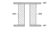
- FIG. 2 is a structural diagram of a square-shaped thermoelectric conversion element formed by Schottky junction of the n-type semiconductor crystallized glass 202 and the p-type semiconductor crystallized glass 203 to the metal electrode 201 by any one of the methods described above.
- a thermoelectric power generation module can be manufactured by electrically connecting these elements in parallel or in series.
Landscapes
- Chemical & Material Sciences (AREA)
- Inorganic Chemistry (AREA)
- Photovoltaic Devices (AREA)
Abstract
Description
る半導体接合素子およびそれを用いた各種デバイスを提供することにある。
Sb2O3、V2O5、P2O5、Fe2О3をそれぞれ重量比で、28%、50%、12%、 10%となるように配合・混合した混合粉末200gを白金ルツボに入れ、電気炉を用いて5~10℃/min(℃/分)の昇温速度で1100℃まで加熱して2時間保持した。保持中は均一なガラスとするために攪拌した。次に、白金ルツボを電気炉から取り出し、予め150~200℃に加熱しておいたステンレス板上に流し込んだ。凝固物はガラス光沢を呈していた。
このガラスにおける4価のバナジウムイオン(V4+)と5価のバナジウムイオン(V5+)の比率を酸化還元滴定法により評価した結果、V4+/V5+<1であった。この結果より、このガラスはp型半導体であることを確認した。
Cu2O、V2O5、Fe2O3、P2O5をそれぞれモル分率で、10%、70%、10%、10%となるように配合・混合した混合粉末200gを白金ルツボに入れ、電気炉を用いて5~10℃/min(℃/分)の昇温速度で1100℃まで加熱して2時間保持した。保持中は均一なガラスとするために攪拌した。次に、白金ルツボを電気炉から取り出し、予め150~200℃に加熱しておいたステンレス板上に流し込んだ。なお、凝固物はガラス光沢を呈していた。
K2CO3、V2O5、Fe2O3、P2O5をそれぞれモル分率で、10%、70%、10%、10%となるように配合・混合した混合粉末200gを白金ルツボに入れ、電気炉を用いて5~10℃/min(℃/分)の昇温速度で1100℃まで加熱して2時間保持した。加熱保持中は均一なガラスとするために攪拌した。次に、白金ルツボを電気炉から取り出し、予め200~300℃に加熱しておいたステンレス板上に流し込んだ。なお、凝固物はガラス光沢を呈していた。
本発明におけるバナジウム酸化物を含有する半導体ガラスは、軟化点が低く、低温での焼成が可能であるため、スクリーン印刷法、インクジェット法、スタンプ法、フォトレジストフィルム法等の簡易な厚膜形成法による成膜が可能である。このため、半導体ガラス、単体半導体、化合物半導体の鏡面研磨面上に、これら半導体と逆極性の半導体ガラス粉末と、有機バインダと、有機溶剤とからなるペーストを前記厚膜形成法により塗布し、加熱により脱溶し、その後、ガラスの軟化点以上の温度で加熱保持することにより焼成し、半導体接合素子を作製することができる。その後、さらに結晶化温度で加熱保持して、半導体ガラスを結晶化させることも可能である。なお、半導体ガラスの焼結性が悪い場合には、用いた半導体ガラスよりも低融点のバナジウム酸化物ガラスを添加するとよい。また、金属の鏡面研磨面上に、前記同様の方法により、半導体膜を形成させることで、ショットキー接合素子を簡易に作製することができる。
図1はバナジウム酸化物からなるn型半導体結晶化ガラス103とp型結晶Si基板104とを、前記のいずれかの方法により接合したp-n半導体接合素子を適用した太陽電池セルの断面図である。また、p型結晶Si基板104の代わりに、p型半導体結晶化ガラス基板を用いることも可能である。n型半導体表面には反射防止膜101と表面電極102,p型半導体裏面には裏面電極105が形成されている。
図2は前記のいずれかの方法により、n型半導体結晶化ガラス202およびp型半導体結晶化ガラス203を金属電極201にショットキー接合して形成されたΠ文字型熱電変換素子の構造図である。この素子をそれぞれ電気的に並列あるいは直列に接合することにより、熱電発電モジュールを作製することができる。
102 表面電極
103,202 n型半導体結晶化ガラス
104 p型Si基板
105 裏面電極
201 金属電極
203 p型半導体結晶化ガラス
Claims (11)
- バナジウム酸化物を含有する異なる極性の半導体ガラス同士が接合されたことを特徴とする半導体接合素子。
- 請求項1において、前記半導体ガラスの少なくとも一部が結晶化されていることを特徴とする半導体接合素子。
- 請求項2において、異なる結晶化率の半導体ガラス同士が接合されたことを特徴とする半導体接合素子。
- バナジウム酸化物を含有する半導体ガラスと、該半導体ガラスと異なる極性の単体半導体あるいは化合物半導体とが接合されたことを特徴とする半導体接合素子。
- バナジウム酸化物を含有する半導体ガラスと、金属とが接合されたことを特徴とするショットキー接合素子。
- 半導体ガラス表面を酸化あるいは還元させることを特徴とする半導体接合素子の製造方法。
- バナジウム酸化物を含有する半導体ガラスと、単体半導体や化合物半導体、あるいは金属とを陽極接合により接合することを特徴とする半導体接合素子の製造方法。
- 請求項1乃至4のいずれかに記載された半導体接合素子を用いたことを特徴とする太陽電池セル。
- 請求項1乃至4のいずれかに記載された半導体接合素子を用いたことを特徴とする熱電変換素子。
- 請求項1乃至4のいずれかに記載された半導体接合素子を用いたことを特徴とするダイオード。
- 請求項1乃至4のいずれかに記載された半導体接合素子を用いたことを特徴とするトランジスタ。
Priority Applications (2)
| Application Number | Priority Date | Filing Date | Title |
|---|---|---|---|
| JP2012534982A JP5651184B2 (ja) | 2010-09-24 | 2011-09-02 | 半導体接合素子の製造方法 |
| US13/813,592 US20130126864A1 (en) | 2010-09-24 | 2011-09-02 | Semiconductor junction element, semiconductor device using it, and manufacturing method of semiconductor junction element |
Applications Claiming Priority (2)
| Application Number | Priority Date | Filing Date | Title |
|---|---|---|---|
| JP2010-213007 | 2010-09-24 | ||
| JP2010213007 | 2010-09-24 |
Publications (1)
| Publication Number | Publication Date |
|---|---|
| WO2012039265A1 true WO2012039265A1 (ja) | 2012-03-29 |
Family
ID=45873754
Family Applications (1)
| Application Number | Title | Priority Date | Filing Date |
|---|---|---|---|
| PCT/JP2011/070007 Ceased WO2012039265A1 (ja) | 2010-09-24 | 2011-09-02 | 半導体接合素子およびそれを用いた半導体デバイス、並びに半導体接合素子の製造方法 |
Country Status (3)
| Country | Link |
|---|---|
| US (1) | US20130126864A1 (ja) |
| JP (1) | JP5651184B2 (ja) |
| WO (1) | WO2012039265A1 (ja) |
Cited By (3)
| Publication number | Priority date | Publication date | Assignee | Title |
|---|---|---|---|---|
| EP2468693A3 (en) * | 2010-12-24 | 2012-08-22 | Hitachi Ltd. | Thermoelectric Conversion Material |
| WO2014073095A1 (ja) * | 2012-11-09 | 2014-05-15 | 株式会社日立製作所 | 熱電変換モジュール及びその製造方法 |
| JP2017011166A (ja) * | 2015-06-24 | 2017-01-12 | リンテック株式会社 | 熱電半導体組成物、並びに熱電変換材料及びその製造方法 |
Families Citing this family (1)
| Publication number | Priority date | Publication date | Assignee | Title |
|---|---|---|---|---|
| US20240405143A1 (en) * | 2023-05-31 | 2024-12-05 | Blue Origin, Llc | Solar Cells Incorporating FeOx Thin-Films |
Citations (5)
| Publication number | Priority date | Publication date | Assignee | Title |
|---|---|---|---|---|
| JPS5927253A (ja) * | 1982-08-06 | 1984-02-13 | Shinei Kk | ガスセンサおよびその製造法 |
| JP2005251917A (ja) * | 2004-03-03 | 2005-09-15 | Denso Corp | 熱電変換素子 |
| JP2005260097A (ja) * | 2004-03-12 | 2005-09-22 | Tdk Corp | 希土類磁石およびその製造方法 |
| JP2005302758A (ja) * | 2004-04-06 | 2005-10-27 | Ismanj:Kk | 熱電発電体 |
| JP2009529798A (ja) * | 2006-03-14 | 2009-08-20 | コラス、テクノロジー、ベスローテン、フェンノートシャップ | 金属基材を含んでなるカルコパイライト半導体系光起電力太陽電池、光起電力太陽電池用の被覆された金属基材、およびその製造方法 |
Family Cites Families (15)
| Publication number | Priority date | Publication date | Assignee | Title |
|---|---|---|---|---|
| JPH0964408A (ja) * | 1995-08-24 | 1997-03-07 | Denso Corp | 半導体装置及びその製造方法 |
| JP4686171B2 (ja) * | 2004-10-29 | 2011-05-18 | 株式会社東芝 | 熱−電気直接変換装置 |
| CN1841425A (zh) * | 2005-03-31 | 2006-10-04 | 华为技术有限公司 | 移动终端购物方法及其系统 |
| JP5024835B2 (ja) * | 2006-03-31 | 2012-09-12 | 公益財団法人北九州産業学術推進機構 | ペルチェ素子を備えた温調容器 |
| ES2651625T3 (es) * | 2007-04-25 | 2018-01-29 | Heraeus Precious Metals North America Conshohocken Llc | Formulaciones para conductores de película gruesa, que comprenden plata y níquel o aleaciones de plata y níquel y celdas solares fabricadas a partir de las mismas |
| JP5525714B2 (ja) * | 2008-02-08 | 2014-06-18 | 日立粉末冶金株式会社 | ガラス組成物 |
| JP2010081806A (ja) * | 2008-09-29 | 2010-04-15 | Tecnisco Ltd | 温度調節流路付きスライド構造 |
| JP5699933B2 (ja) * | 2009-03-27 | 2015-04-15 | 日立化成株式会社 | ガラス組成物およびそれを用いた導電性ペースト組成物、電極配線部材と電子部品 |
| JP2011014373A (ja) * | 2009-07-02 | 2011-01-20 | Hitachi Powdered Metals Co Ltd | 導電性材料及びこれを用いたLiイオン二次電池用正極材料 |
| US20110180139A1 (en) * | 2010-01-25 | 2011-07-28 | Hitachi Chemical Company, Ltd. | Paste composition for electrode and photovoltaic cell |
| US20110195541A1 (en) * | 2010-02-05 | 2011-08-11 | Hitachi Chemical Company, Ltd. | Composition for forming n-type diffusion layer, method for forming n-type diffusion layer, and method for producing photovoltaic cell |
| JP5416631B2 (ja) * | 2010-03-25 | 2014-02-12 | 株式会社日立製作所 | アルミニウム電極配線用のガラス組成物と導電性ペースト、そのアルミニウム電極配線を具備する電子部品、及び、この電子部品の製造方法 |
| EP2636070A4 (en) * | 2010-10-28 | 2014-04-02 | Heraeus Precious Metals North America Conshohocken Llc | SOLAR CELL METALLIZATION WITH A METAL SUPPLEMENT |
| JP5537402B2 (ja) * | 2010-12-24 | 2014-07-02 | 株式会社日立製作所 | 熱電変換材料 |
| CN103890960A (zh) * | 2011-07-25 | 2014-06-25 | 日立化成株式会社 | 元件及太阳能电池 |
-
2011
- 2011-09-02 WO PCT/JP2011/070007 patent/WO2012039265A1/ja not_active Ceased
- 2011-09-02 US US13/813,592 patent/US20130126864A1/en not_active Abandoned
- 2011-09-02 JP JP2012534982A patent/JP5651184B2/ja not_active Expired - Fee Related
Patent Citations (5)
| Publication number | Priority date | Publication date | Assignee | Title |
|---|---|---|---|---|
| JPS5927253A (ja) * | 1982-08-06 | 1984-02-13 | Shinei Kk | ガスセンサおよびその製造法 |
| JP2005251917A (ja) * | 2004-03-03 | 2005-09-15 | Denso Corp | 熱電変換素子 |
| JP2005260097A (ja) * | 2004-03-12 | 2005-09-22 | Tdk Corp | 希土類磁石およびその製造方法 |
| JP2005302758A (ja) * | 2004-04-06 | 2005-10-27 | Ismanj:Kk | 熱電発電体 |
| JP2009529798A (ja) * | 2006-03-14 | 2009-08-20 | コラス、テクノロジー、ベスローテン、フェンノートシャップ | 金属基材を含んでなるカルコパイライト半導体系光起電力太陽電池、光起電力太陽電池用の被覆された金属基材、およびその製造方法 |
Non-Patent Citations (1)
| Title |
|---|
| A.AXELEVITCH ET AL.: "Preparation and investigation of VOx thin films of n- and p-types", THIN SOLID FILMS, vol. 515, no. 24, 11 April 2007 (2007-04-11), pages 8446 - 8449, XP022265890, DOI: doi:10.1016/j.tsf.2007.04.011 * |
Cited By (5)
| Publication number | Priority date | Publication date | Assignee | Title |
|---|---|---|---|---|
| EP2468693A3 (en) * | 2010-12-24 | 2012-08-22 | Hitachi Ltd. | Thermoelectric Conversion Material |
| US8802963B2 (en) | 2010-12-24 | 2014-08-12 | Hitachi, Ltd. | Thermoelectric conversion material |
| WO2014073095A1 (ja) * | 2012-11-09 | 2014-05-15 | 株式会社日立製作所 | 熱電変換モジュール及びその製造方法 |
| JPWO2014073095A1 (ja) * | 2012-11-09 | 2016-09-08 | 株式会社日立製作所 | 熱電変換モジュール及びその製造方法 |
| JP2017011166A (ja) * | 2015-06-24 | 2017-01-12 | リンテック株式会社 | 熱電半導体組成物、並びに熱電変換材料及びその製造方法 |
Also Published As
| Publication number | Publication date |
|---|---|
| US20130126864A1 (en) | 2013-05-23 |
| JP5651184B2 (ja) | 2015-01-07 |
| JPWO2012039265A1 (ja) | 2014-02-03 |
Similar Documents
| Publication | Publication Date | Title |
|---|---|---|
| TWI505523B (zh) | Thermoelectric conversion of composite materials, the use of its thermoelectric conversion material slurry, and the use of its thermoelectric conversion module | |
| JP5651184B2 (ja) | 半導体接合素子の製造方法 | |
| Singh et al. | High performance perovskite solar cell via multi-cycle low temperature processing of lead acetate precursor solutions | |
| TWI469924B (zh) | 新穎化合物半導體及其應用 | |
| TWI469928B (zh) | 新穎化合物半導體及其應用 | |
| TW201838214A (zh) | 熱電變換模組及其製造方法 | |
| TWI465399B (zh) | 新穎化合物半導體及其應用 | |
| TWI469930B (zh) | 新穎化合物半導體及其應用 | |
| TWI467788B (zh) | 新穎化合物半導體及其應用 | |
| TWI469927B (zh) | 新穎化合物半導體及其應用 | |
| TWI469931B (zh) | 新穎化合物半導體及其應用 | |
| KR20130108856A (ko) | 열전 반도체 모듈 및 이의 제조방법 | |
| US20200321502A1 (en) | Power generation element, power generation module, power generation device, power generation system, and method for manufacturing power generation element | |
| CN102191563B (zh) | 共掺杂的硅基杂质中间带材料的制备方法 | |
| TWI457287B (zh) | 新穎的化合物半導體及其應用 | |
| KR20090090843A (ko) | 실리콘 태양전지 제조용 납 프리 유리 프릿 분말 및 그제조방법과 이를 포함하는 금속 페이스트 조성물 및 실리콘태양전지 | |
| JP2014212216A (ja) | 太陽光発電モジュール | |
| RODRIGUEZ LAZCANO et al. | Thin films of AgIn5 (S/Se) 8 prepared in a two stage process | |
| JP2015088679A (ja) | 量子ドット構造体、量子ドット構造体の製造方法および量子ドット構造体を用いた太陽電池モジュール |
Legal Events
| Date | Code | Title | Description |
|---|---|---|---|
| 121 | Ep: the epo has been informed by wipo that ep was designated in this application |
Ref document number: 11826711 Country of ref document: EP Kind code of ref document: A1 |
|
| WWE | Wipo information: entry into national phase |
Ref document number: 2012534982 Country of ref document: JP |
|
| WWE | Wipo information: entry into national phase |
Ref document number: 13813592 Country of ref document: US |
|
| NENP | Non-entry into the national phase |
Ref country code: DE |
|
| 122 | Ep: pct application non-entry in european phase |
Ref document number: 11826711 Country of ref document: EP Kind code of ref document: A1 |