WO2012029686A1 - 照明装置および表示装置 - Google Patents
照明装置および表示装置 Download PDFInfo
- Publication number
- WO2012029686A1 WO2012029686A1 PCT/JP2011/069385 JP2011069385W WO2012029686A1 WO 2012029686 A1 WO2012029686 A1 WO 2012029686A1 JP 2011069385 W JP2011069385 W JP 2011069385W WO 2012029686 A1 WO2012029686 A1 WO 2012029686A1
- Authority
- WO
- WIPO (PCT)
- Prior art keywords
- adhesive member
- light source
- reflection sheet
- substrate
- led
- Prior art date
- Legal status (The legal status is an assumption and is not a legal conclusion. Google has not performed a legal analysis and makes no representation as to the accuracy of the status listed.)
- Ceased
Links
Images




Classifications
-
- G—PHYSICS
- G02—OPTICS
- G02F—OPTICAL DEVICES OR ARRANGEMENTS FOR THE CONTROL OF LIGHT BY MODIFICATION OF THE OPTICAL PROPERTIES OF THE MEDIA OF THE ELEMENTS INVOLVED THEREIN; NON-LINEAR OPTICS; FREQUENCY-CHANGING OF LIGHT; OPTICAL LOGIC ELEMENTS; OPTICAL ANALOGUE/DIGITAL CONVERTERS
- G02F1/00—Devices or arrangements for the control of the intensity, colour, phase, polarisation or direction of light arriving from an independent light source, e.g. switching, gating or modulating; Non-linear optics
- G02F1/01—Devices or arrangements for the control of the intensity, colour, phase, polarisation or direction of light arriving from an independent light source, e.g. switching, gating or modulating; Non-linear optics for the control of the intensity, phase, polarisation or colour
- G02F1/13—Devices or arrangements for the control of the intensity, colour, phase, polarisation or direction of light arriving from an independent light source, e.g. switching, gating or modulating; Non-linear optics for the control of the intensity, phase, polarisation or colour based on liquid crystals, e.g. single liquid crystal display cells
- G02F1/133—Constructional arrangements; Operation of liquid crystal cells; Circuit arrangements
- G02F1/1333—Constructional arrangements; Manufacturing methods
- G02F1/1335—Structural association of cells with optical devices, e.g. polarisers or reflectors
- G02F1/1336—Illuminating devices
- G02F1/133602—Direct backlight
- G02F1/133603—Direct backlight with LEDs
-
- G—PHYSICS
- G02—OPTICS
- G02F—OPTICAL DEVICES OR ARRANGEMENTS FOR THE CONTROL OF LIGHT BY MODIFICATION OF THE OPTICAL PROPERTIES OF THE MEDIA OF THE ELEMENTS INVOLVED THEREIN; NON-LINEAR OPTICS; FREQUENCY-CHANGING OF LIGHT; OPTICAL LOGIC ELEMENTS; OPTICAL ANALOGUE/DIGITAL CONVERTERS
- G02F1/00—Devices or arrangements for the control of the intensity, colour, phase, polarisation or direction of light arriving from an independent light source, e.g. switching, gating or modulating; Non-linear optics
- G02F1/01—Devices or arrangements for the control of the intensity, colour, phase, polarisation or direction of light arriving from an independent light source, e.g. switching, gating or modulating; Non-linear optics for the control of the intensity, phase, polarisation or colour
- G02F1/13—Devices or arrangements for the control of the intensity, colour, phase, polarisation or direction of light arriving from an independent light source, e.g. switching, gating or modulating; Non-linear optics for the control of the intensity, phase, polarisation or colour based on liquid crystals, e.g. single liquid crystal display cells
- G02F1/133—Constructional arrangements; Operation of liquid crystal cells; Circuit arrangements
- G02F1/1333—Constructional arrangements; Manufacturing methods
- G02F1/1335—Structural association of cells with optical devices, e.g. polarisers or reflectors
- G02F1/1336—Illuminating devices
- G02F1/133602—Direct backlight
- G02F1/133605—Direct backlight including specially adapted reflectors
-
- G—PHYSICS
- G02—OPTICS
- G02F—OPTICAL DEVICES OR ARRANGEMENTS FOR THE CONTROL OF LIGHT BY MODIFICATION OF THE OPTICAL PROPERTIES OF THE MEDIA OF THE ELEMENTS INVOLVED THEREIN; NON-LINEAR OPTICS; FREQUENCY-CHANGING OF LIGHT; OPTICAL LOGIC ELEMENTS; OPTICAL ANALOGUE/DIGITAL CONVERTERS
- G02F2202/00—Materials and properties
- G02F2202/28—Adhesive materials or arrangements
Definitions
- the present invention relates to a lighting device and a display device.
- the liquid crystal display panel that displays images does not emit light, so an illumination device is installed on the back side of the liquid crystal display panel (the side opposite to the display surface side of the liquid crystal display panel)
- the liquid crystal display panel is illuminated with light from the illumination device.
- the illuminating device installed in the back surface side of a liquid crystal display panel is called the backlight unit etc., for example.
- a cold cathode fluorescent lamp in which mercury or xenon is enclosed in a fluorescent tube is known.
- the cold cathode fluorescent lamp is used as the light source of the backlight unit, there are disadvantages that the light emission luminance and life are insufficient, and that the luminance on the low-pressure side is low, making it difficult to obtain a uniform light emission. It was.
- a backlight unit using an LED (light emitting diode) package as a light source has been proposed in place of the cold cathode fluorescent lamp.
- the light source used for the backlight unit is an LED package, in addition to eliminating the above-described disadvantages, it is possible to easily reduce power consumption and to reduce the environmental load.
- the backlight unit is roughly classified into two types, an edge light type and a direct type.
- An edge-light type backlight unit has a light guide plate arranged directly under a liquid crystal display panel (a region facing the back surface of the liquid crystal display panel), and a light source arranged so as to face a predetermined side end surface of the light guide plate. It is.
- the edge light type backlight unit when light is emitted from the light source, the light from the light source is introduced into the light guide plate through a predetermined side end surface of the light guide plate. Then, the light introduced into the light guide plate is emitted from the front surface of the light guide plate (the surface directed to the liquid crystal display panel side) to illuminate the liquid crystal display panel.
- the direct type backlight unit has a light source arranged directly under the liquid crystal display panel.
- Such a direct type backlight unit is advantageous for illuminating a large area with high output, and is often used for a large-sized liquid crystal display device.
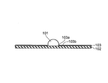
- the reflection sheet 103 is disposed on the mounting surface of the substrate 102.
- an exposure hole 103 a is formed in the reflection sheet 103, and the LED package 101 is exposed (projected) from the exposure hole 103 a of the reflection sheet 103.
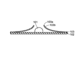
- the exposed hole of the reflective sheet 103 is shown in FIG.
- the edge portion 103b of 103a may be warped and floated.
- the reflection of the light by the reflection sheet 103 is not performed favorably in the peripheral region of the LED package 101.
- the luminance of the region corresponding to the peripheral region of the LED package 101 is lowered, and luminance unevenness occurs.
- the present invention has been made to solve the above-described problems, and an object thereof is to provide an illumination device and a display device capable of suppressing the occurrence of luminance unevenness.
- an illumination device includes a light source substrate on which a light source is mounted, a reflection sheet having an exposure hole for exposing the light source, and the reflection sheet and the light source substrate. And an adhesive member to be bonded.
- An adhesive member is disposed so as to surround the periphery of the light source, and an edge portion of the exposed hole of the reflection sheet is bonded to the light source substrate via the adhesive member.
- the adhesive member is disposed so as to surround the periphery of the light source, and the edge portion of the exposed hole of the reflection sheet is adhered to the light source substrate via the adhesive member. Further, warpage (lifting) of the edge portion of the exposed hole of the reflection sheet can be reduced or eliminated. Thereby, reflection of the light by a reflective sheet is favorably performed in the surrounding area of the light source. As a result, it is possible to suppress the inconvenience that the luminance unevenness occurs due to the decrease in the luminance of the region corresponding to the peripheral region of the light source.
- the adhesive member is formed in an annular shape that can surround the entire circumference of the light source. If comprised in this way, the edge part of the exposure hole of a reflection sheet can be adhere
- the adhesive member is formed in a shape along the shape of the edge portion of the exposed hole of the reflection sheet. If comprised in this way, the part (namely, edge part of the exposed hole of a reflection sheet) which generate
- the shape of the adhesive member is preferably an annular shape.
- the shape of the edge portion of the exposure hole of the reflection sheet is a quadrangular ring shape, and therefore, the shape of the adhesive member is preferably a square ring shape.
- the exposure hole of the reflection sheet includes a plurality of exposure holes
- the adhesive member includes the same number of adhesive members as the plurality of exposure holes of the reflection sheet. It is preferable that each edge portion of the exposure hole is individually bonded to the light source substrate via an adhesive member.
- the exposure hole of the reflection sheet includes a plurality of exposure holes. That is, the light source includes the same number of light sources as the exposure holes of the reflection sheet, and each of the plurality of light sources individually from the exposure holes of the reflection sheet. It is that it is exposed.
- the plurality of adhesive members may be integrally connected to each other. If comprised in this way, when the protective film is affixed on the some adhesive member before use, the operation
- an adhesive member may be sandwiched between the edge portion of the exposed hole of the reflection sheet and the light source substrate.
- a double-sided tape or the like is preferably used as the adhesive member. If comprised in this way, the edge part of the exposure hole of a reflective sheet and the light source board
- the entire portion of the adhesive member is the edge portion of the exposed hole of the reflective sheet and the light source substrate so that the adhesive member is not exposed. More preferably, it is sandwiched between the two. If comprised in this way, light will not be absorbed by the adhesive member.
- a groove portion is formed in the portion of the light source substrate that overlaps with the edge portion of the exposure hole of the reflection sheet.
- the reflective sheet and the light source substrate may be bonded to each other through an adhesive member fitted in the groove portion of the light source substrate.
- the groove portion of the light source substrate becomes a positioning portion for positioning the adhesive member when the adhesive member is bonded to the light source substrate. For this reason, an adhesive member can be adhere
- the predetermined portion of the adhesive member bonded to the light source substrate covers the edge portion of the exposed hole of the reflective sheet, and the predetermined portion of the adhesive member is the edge portion of the exposed hole of the reflective sheet. It may be adhered to. That is, the edge portion of the exposed hole of the reflection sheet may be sandwiched between the light source substrate and the adhesive member. If comprised in this way, since a reflective sheet and the mounting surface of a light source board
- the surface of the adhesive member opposite to the surface bonded to the reflection sheet and the light source substrate is a light reflection surface. If comprised in this way, although the surface on the opposite side to the surface currently adhere
- the display device includes the illumination device according to the first aspect and a display panel illuminated with light from the illumination device.
- an illumination device and a display device capable of suppressing the occurrence of luminance unevenness.
- FIG. 3 is a plan view showing a state where a plurality of adhesive members of the backlight unit according to the first embodiment of the present invention are bonded to an LED substrate (a diagram in the case where the plurality of adhesive members are integrally connected to each other).
- FIG. 4 is a plan view showing a state where a plurality of adhesive members of the backlight unit according to the first embodiment of the present invention are bonded to an LED substrate (a diagram in a case where the plurality of adhesive members are not integrally connected to each other). It is a figure for demonstrating the modification of the adhesive member of the backlight unit by 1st Embodiment of this invention. It is a figure for demonstrating the modification of the adhesive member of the backlight unit by 1st Embodiment of this invention. It is sectional drawing showing the adhesion structure between the reflective sheet and LED board of the backlight unit by 2nd Embodiment of this invention.
- This display device is a liquid crystal display device, and as shown in FIG. 1, is installed on a liquid crystal display panel (illuminated body) 10 for displaying an image and a back surface side opposite to the display surface side of the liquid crystal display panel 10.
- the backlight unit 20 is provided at least.
- the liquid crystal display panel 10 is an example of the “display panel” in the present invention
- the backlight unit 20 is an example of the “illuminating device” in the present invention.
- the liquid crystal display panel 10 has a display area where an image is actually displayed and a non-display area which is an outer edge area of the display area. A plurality of pixels arranged in a matrix are formed in the display area of the liquid crystal display panel 10.
- Each of the plurality of pixels is driven by a switching element, a pixel electrode, a common electrode, and the like. Note that the switching element, the pixel electrode, and the common electrode are not shown in order to make the drawing easy to see, and wirings that are electrically connected to them are not shown.
- the switching element is made of a TFT (thin film transistor), the gate of the switching element is connected to a gate line (scanning line), and the source of the switching element is connected to a source line (data line).
- a pixel electrode is connected to the drain of the switching element, a common electrode is disposed so as to face the pixel electrode, and a liquid crystal (not shown) is sandwiched between the pixel electrode and the common electrode.
- the switching elements are individually provided for each pixel, and the pixel electrodes are also individually provided for each pixel.
- the common electrode is common to each pixel.
- the backlight unit 20 employs a direct type system, emits white backlight light in a planar shape, and uniformly illuminates the back surface of the liquid crystal display panel 10 with the backlight light. ing.
- the optical property (light transmittance) of the liquid crystal is changed for each pixel based on the video signal. Specifically, in each pixel, an electric field is generated between the pixel electrode and the common electrode by supplying predetermined power to the pixel electrode via the switching element. The orientation of the liquid crystal, that is, the transmittance of light transmitted through the liquid crystal is changed by the electric field generated between the pixel electrode and the common electrode.
- the liquid crystal display panel 10 includes at least two transparent substrates 11 and 12.
- One transparent substrate 11 is referred to as an active matrix substrate, and the other transparent substrate 12 may be referred to as a counter substrate because it is disposed opposite to the transparent substrate 11, or a color filter.
- a switching element and a pixel electrode are formed, and a gate line (scanning line) and a source line (data line) electrically connected to them are also formed.
- a common electrode is formed on a predetermined surface of the other transparent substrate 12.
- a color filter is further formed on the predetermined surface of the other transparent substrate 12 as necessary.
- Each predetermined surface of the two transparent electrodes 11 and 12 is covered with an alignment film (not shown) capable of aligning the liquid crystal in a specific direction.
- the two transparent substrates 11 and 12 are bonded to each other via a seal material (not shown) so that their predetermined surfaces face each other.
- a liquid crystal is sealed between the two transparent substrates 11 and 12.
- the liquid crystal is sandwiched between the pixel electrode and the common electrode (between the alignment film covering the predetermined surface of one transparent substrate 11 and the alignment film covering the predetermined surface of the other transparent electrode 12). ing.
- the outer sizes of the two transparent substrates 11 and 12 are different from each other, and the outer size of the transparent substrate 11 is larger than the outer size of the transparent substrate 12. Accordingly, the two transparent substrates 11 and 12 are bonded to each other, but the predetermined ends of the transparent substrates 11 and 12 do not match each other, and a part of the predetermined surface of the transparent substrate 11 is separated from the transparent substrate 12. Exposed. The exposed portion of the predetermined surface of the transparent substrate 11 is a region of a non-display area, and is used for electrically connecting a driver (not shown) to the transparent substrate 11.
- a polarizing sheet 13 that transmits only light waves in a specific vibration direction is attached to each of the surfaces of the two transparent substrates 11 and 12 opposite to the predetermined surfaces (surfaces on the liquid crystal side). Yes.
- the transmission axis directions of the two polarizing sheets 13 are shifted from each other by about 90 °.
- the backlight unit 20 installed on the back side of the liquid crystal display panel 10 includes at least a back chassis 21, a light emitting module 22, a reflection sheet 23, and an optical sheet 24.
- the back chassis 21 is formed in a substantially box shape with the liquid crystal display panel 10 side opened. That is, the back chassis 21 has a bottom portion 21a having a substantially rectangular shape in plan view (when viewed from the liquid crystal display panel 10 side), and a side portion 21b standing on the outer periphery of the bottom portion 21a. Will be. And the area
- the light emitting module 22 is for generating light that is the basis of backlight light, and is housed in a housing area of the back chassis 21 and is fixed to the bottom 21 a of the back chassis 21. In the state where the backlight unit 20 is installed on the back side of the liquid crystal display panel 10, the light emitting module 22 is disposed directly below the liquid crystal display panel 10 (region facing the back side of the liquid crystal display panel 10).
- the light emitting module 22 has the same LED substrate (having two or more LED packages 25 each emitting white LED light as a light source, and the two or more LED packages 25 are formed in a strip shape.
- the light source board 26 is mounted on the mounting surface. Further, the two or more LED packages 25 are arranged in a line along the longitudinal direction of the LED substrate 26 and are connected in series.
- the method of making the LED light emitted from the LED package 25 white is not particularly limited.
- a combination of a phosphor that converts blue LED light into yellow and a blue LED is used as the LED package 25.
- a combination of a phosphor that converts blue LED light into green and red and a blue LED may be used as the LED package 25.
- a combination of three types of LEDs, a blue LED, a green LED, and a red LED may be used as the LED package 25.
- the number of LED packages 25 mounted on the mounting surface of the same LED substrate 26 is not particularly limited, and can be changed according to the application.
- the plurality of light emitting modules 22 are accommodated in the accommodation area of the back chassis 21, but the plurality of light emitting modules 22 are parallel to the bottom surface of the bottom portion 21 a of the back chassis 21. They are two-dimensionally arranged at predetermined intervals in the X direction (longitudinal direction of the back chassis 21) and the Y direction (short direction of the back chassis 21). In this state, the longitudinal direction of the LED board 26 and the X direction coincide with each other, and the short side direction and the Y direction of the LED board 26 coincide with each other.
- the light emitting modules 22 adjacent in the X direction are electrically connected to each other via a connector (not shown).
- the LED boards 26 included in each of the one light emitting module 22 and the other light emitting module 22 adjacent to each other in the X direction are electrically connected to each other via the connector.
- the reflection sheet 23 is for reflecting the LED light emitted from the LED package 25 toward the liquid crystal display panel 10, and is housed in the housing area of the back chassis 21 together with the light emitting module 22.
- the structure of the reflection sheet 23 includes a bottom portion 23a having a substantially rectangular shape in plan view, and an obliquely inclined side portion 23b standing on the outer periphery of the bottom portion 23a.
- the bottom portion 23 a of the reflection sheet 23 is placed on the bottom surface of the bottom portion 21 a of the back chassis 21 with the LED substrate 26 interposed therebetween. That is, the bottom portion 23 a of the reflection sheet 23 covers the mounting surface of the LED substrate 26 (including the portion of the bottom surface of the bottom portion 21 a of the back chassis 21 that does not overlap the LED substrate 26).
- the side portion 23 b of the reflection sheet 23 covers the inner side surface of the side portion 21 b of the back chassis 21.
- the LED package 25 mounted on the LED substrate 26 is also covered with the bottom 23a of the reflection sheet 23. For this reason, the light emission of the LED package 25 is inhibited. Accordingly, the same number of exposed holes 23c having circular openings are formed in the bottom 23a of the reflection sheet 23 so that the LED package 25 is exposed to the liquid crystal display panel 10 side. One LED package 25 is exposed (projected) to the liquid crystal display panel 10 side from each of the exposed holes 23 c of the reflection sheet 23.
- the optical sheet 24 is a sheet group including a diffusion sheet, a prism sheet, and the like, and is disposed so as to close the opening of the back chassis 21. That is, the optical sheet 24 is disposed on the side facing the bottom surface of the bottom portion 21a of the back chassis 21 (the bottom surface of the bottom portion 23a of the reflection sheet 23), thereby covering the light emitting module 22 from the liquid crystal display panel 10 side. ing. Therefore, after the LED light emitted from the LED package 25 is incident on the optical sheet 24 to be diffused or condensed, the back surface of the liquid crystal display panel 10 is illuminated.
- the type and the number of sheets used of the optical sheet 24 are appropriately changed according to the application.
- the reflection sheet 23 and the LED substrate 26 are bonded and fixed to each other using an adhesive member 27 (a member including an adhesive or the like) 27 as shown in FIGS.
- an adhesive member 27 a member including an adhesive or the like
- FIG. 2 is not a cross-sectional view, hatching is applied to a portion corresponding to the adhesive member 27 in order to make the drawing easy to see.
- the adhesive member 27 for adhering the reflective sheet 23 and the LED substrate 26 to each other is a double-sided tape and has a structure in which an adhesive is applied to both surfaces of a base material made of polyethylene or the like.
- Examples of the pressure-sensitive adhesive applied to both surfaces of the substrate include acrylic pressure-sensitive adhesives, fluororesin-based pressure-sensitive adhesives, and siloxane-based pressure-sensitive adhesives.
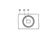
- the adhesive member 27 has a shape that can surround the entire periphery of the LED package 25. Specifically, as the shape of the adhesive member 27, an annular shape along the shape of the edge portion 23d of the exposed hole 23c of the reflective sheet 23 (an annular shape along the opening shape of the exposed hole 23c of the reflective sheet 23) and Has been.
- the adhesive sheet 27 is adhered to the LED substrate 26 by the adhesive member 27.
- the adhesive member 27 is disposed so as to surround the entire periphery of the LED package 25, and the edge portion 23d of the exposure hole 23c of the reflective sheet 23 is provided. Between the LED board 26 and the LED board 26. That is, the edge portion 23 d of the exposure hole 23 c of the reflection sheet 23 is bonded to the LED substrate 26 via the bonding member 27.
- the number of the exposed holes 23c of the reflective sheet 23 (the number of the LED packages 25) is plural, but the same number of adhesive members 27 as the plural exposed holes 23c of the reflective sheet 23 are used. Is used.
- Each of the edge portions 23 d of the plurality of exposed holes 23 c of the reflection sheet 23 is individually bonded to the LED substrate 26 via the bonding member 27.
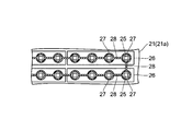
- the plurality of adhesive members 27 are integrally connected to each other via a connecting portion 28, for example, as shown in FIG. Of course, as shown in FIG. 5, the plurality of adhesive members 27 may be independent from each other. 4 and 5 are not cross-sectional views, but portions corresponding to the adhesive members 27 are hatched to make the drawings easy to see.
- the adhesive member 27 is disposed so as to surround the LED package 25, and the edge portion 23 d of the exposure hole 23 c of the reflection sheet 23 is connected to the LED substrate 26 via the adhesive member 27.
- warping (lifting) of the edge portion 23d of the exposure hole 23c of the reflection sheet 23 can be reduced or eliminated.
- the reflection of light by the reflection sheet 23 is favorably performed in the peripheral region of the LED package 25.
- the adhesive member 27 is formed in an annular shape that can surround the entire periphery of the LED package 25, the edge portion 23d of the exposure hole 23c of the reflection sheet 23 is formed. Can be adhered to the LED substrate 26 over the entire circumference. Thereby, generation
- the adhesive member 27 is formed in a shape along the shape of the edge portion 23d of the exposure hole 23c of the reflection sheet 23.
- a portion where warpage is likely to occur that is, the edge portion 23 d of the exposure hole 23 c of the reflection sheet 23) can be reliably bonded to the LED substrate 26.
- the double-sided tape is used as the adhesive member 27 by sandwiching the adhesive member 27 between the edge portion 23d of the exposed hole 23c of the reflection sheet 23 and the LED substrate 26, The edge portion 23d of the exposed hole 23c of the reflection sheet 23 and the LED substrate 26 can be easily bonded.
- the adhesive member 27 when the adhesive member 27 is sandwiched between the edge portion 23d of the exposed hole 23c of the reflective sheet 23 and the LED substrate 26, the entire portion of the adhesive member 27 is exposed to the exposed hole of the reflective sheet 23 so that the adhesive member 27 is not exposed. By sandwiching between the edge portion 23d of the LED 23c and the LED substrate 26, the light is not absorbed by the adhesive member 27.
- the plurality of adhesive members 27 are prepared, and the edge portions 23 d of the plurality of exposed holes 23 c of the reflection sheet 23 are individually bonded to the LED substrate 26 by the adhesive members 27. This makes it difficult for all of the edge portions 23d of the plurality of exposed holes 23c of the reflection sheet 23 to be warped, and unevenness of luminance occurs over the entire surface of the illumination light emitting surface (the surface of the optical sheet 24 on the liquid crystal display panel 10 side). Occurrence can be suppressed.
- a protective film (a film that protects the adhesive) is formed from the plurality of adhesive members 27.
- the work of peeling is only once. Thereby, the operation
- a part of the adhesive member 27 may be cut. That is, the adhesive member 27 may not surround the entire periphery of the LED package 25.
- FIG. 6 is not a cross-sectional view, the portion corresponding to the adhesive member 27 is hatched to make the drawing easy to see.
- the opening shape of the exposure hole 23c of the reflection sheet 23 is a shape different from circular shape
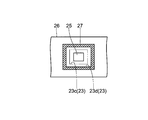
- the shape of the edge portion 23 d of the exposed hole 23 c of the reflective sheet 23 is a quadrangular ring.
- the shape of 27 is preferably formed in a square ring shape.
- FIG. 7 is not a cross-sectional view, a portion corresponding to the adhesive member 27 is hatched to make the drawing easy to see.
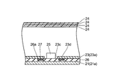
- a portion of the LED substrate 26 that overlaps with the edge portion 23 d of the exposure hole 23 c of the reflection sheet 23 is placed from the mounting surface of the LED substrate 26 to the opposite mounting surface (the mounting surface and the mounting surface). Is formed a non-penetrating concave groove 26a dug toward the opposite surface.
- the groove portion 26a of the LED substrate 26 has an annular shape along the shape of the edge portion 23d of the exposed hole 23c of the reflective sheet 23 (an annular shape along the opening shape of the exposed hole 23c of the reflective sheet 23).
- the LED package 25 is surrounded all around. Further, the groove portion 26 a of the LED substrate 26 has a groove depth substantially equal to the thickness of the adhesive member 27.
- the adhesive member 27 is fitted into the groove 26 a of the LED substrate 26, and the edge portion 23 d of the exposed hole 23 c of the reflective sheet 23 and the LED substrate 26 are adhered by the adhesive member 27. Yes.
- the adhesive member 27 is fitted into the groove portion 26a of the LED substrate 26 by bonding the edge portion 23d of the exposure hole 23c of the reflective sheet 23 and the LED substrate 26 using the above-described adhesive structure. Therefore, the protruding amount of the adhesive member 27 from the mounting surface of the LED substrate 26 is reduced (or the protruding of the adhesive member 27 from the mounting surface of the LED substrate 26 is eliminated). Thereby, since the bottom part 23a of the reflective sheet 23 and the mounting surface of the LED substrate 26 can be brought into close contact with each other, the reflective sheet 23 is stably held.
- the groove 26 a of the LED substrate 26 becomes a positioning portion for positioning the adhesive member 27 when the adhesive member 27 is bonded to the LED substrate 26. For this reason, the adhesive member 27 can be bonded to the LED substrate 26 without being displaced.
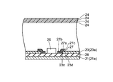
- the bottom 23 a of the reflection sheet 23 is in close contact with the mounting surface of the LED substrate 26, and a predetermined portion 27 a of the adhesive member 27 bonded to the LED substrate 26 is the reflection sheet 23. It extends so as to cover the edge portion 23d of the exposed hole 23c.
- the predetermined portion 27 a of the adhesive member 27 is bonded to the edge portion 23 d of the exposure hole 23 c of the reflection sheet 23. That is, in this embodiment, the adhesive member 27 is not sandwiched between the LED board 26 and the edge portion 23d of the exposure hole 23c of the reflection sheet 23, but the edge portion 23d of the exposure hole 23c of the reflection sheet 23 is not sandwiched. It is in a state of being sandwiched between the LED substrate 26 and the adhesive member 27.
- attached on the reflective sheet 23 and LED board 26 among the adhesive members 27 is made into the light reflection surface 27b.
- the surface of the adhesive member 27 is a light reflecting surface 27b by attaching the reflecting sheet 27c.
- the edge 23d of the exposure hole 23c of the reflection sheet 23 and the LED substrate 26 are bonded to each other using the bonding structure as described above, thereby mounting the bottom 23a of the reflection sheet 23 and the mounting surface of the LED substrate 26. And the reflection sheet 23 is stably held.
- the surface of the adhesive member 27 is exposed.
- the surface of the adhesive member 27 is a light reflecting surface 27b, the light on the surface of the adhesive member 27 (that is, the light reflecting surface 27b). Absorption is low. For this reason, it can suppress that loss light increases.
- the present invention is not limited thereto, and the lighting device installed in a display device other than the liquid crystal display device is used.
- the present invention may be applied.
- Liquid crystal display panel (display panel) 20 Backlight unit (lighting device) 23 Reflective sheet 23c Exposed hole 23d Edge 25 LED package (light source) 26 LED board (light source board) 26a Groove portion 27 Adhesive member 27a Predetermined portion 27b Light reflecting surface 28 Connecting portion
Landscapes
- Physics & Mathematics (AREA)
- Nonlinear Science (AREA)
- Mathematical Physics (AREA)
- Chemical & Material Sciences (AREA)
- Crystallography & Structural Chemistry (AREA)
- General Physics & Mathematics (AREA)
- Optics & Photonics (AREA)
- Planar Illumination Modules (AREA)
Abstract
輝度ムラの発生を抑制することが可能な照明装置を提供する。この照明装置は、LEDパッケージ(25)が搭載されたLED基板(26)と、LEDパッケージ(25)を露出させるための露出穴(23c)を有する反射シート(23)と、反射シート(23)およびLED基板(26)を互いに接着する接着部材(27)とを備えている。そして、LEDパッケージ(25)の周囲を囲むように接着部材(27)が配置されており、露出穴(23c)の縁部分(23d)が接着部材(27)を介してLED基板(26)に接着されている。
Description
本発明は、照明装置および表示装置に関する。
表示装置の一つである液晶表示装置では、映像を表示する液晶表示パネルが非発光であるため、液晶表示パネルの裏面側(液晶表示パネルの表示面側とは反対側)に照明装置を設置し、その照明装置からの光で液晶表示パネルを照明するようになっている。なお、液晶表示パネルの裏面側に設置される照明装置は、たとえば、バックライトユニットなどと称されている。
バックライトユニットに使用する光源としては、水銀やキセノンを蛍光管の内部に封入した冷陰極蛍光ランプが知られている。しかし、冷陰極蛍光ランプをバックライトユニットの光源とした場合、発光輝度や寿命が不十分となり、さらに、低圧側の輝度が低くなることで均整のとれた発光が得られ難くなるという不都合があった。
そこで、このような不都合を解消するために、冷陰極蛍光ランプに代えて、LED(発光ダイオード)パッケージを光源としたバックライトユニットが提案されている。バックライトユニットに使用する光源をLEDパッケージとすると、上述した不都合が解消されることに加えて、低消費電力化が容易に図られ、環境負荷の低減も実現できる。
また、バックライトユニットは、大別するとエッジライト型方式と直下型方式との2つに分類される。
エッジライト型のバックライトユニットは、液晶表示パネルの直下(液晶表示パネルの裏面と対向する領域)に導光板を配置し、その導光板の所定の側端面と対向するように光源を配置したものである。このエッジライト型のバックライトユニットでは、光源から光が発せられると、光源からの光が導光板の所定の側端面を介して導光板内に導入される。そして、導光板内に導入された光が導光板の前面(液晶表示パネル側に向けられた面)から出射されることで液晶表示パネルが照明される。
一方、直下型のバックライトユニットは、液晶表示パネルの直下に光源を配置したものである。このような直下型のバックライトユニットは、大面積を高出力で照明するのに有利であって、大型サイズの液晶表示装置に使用されることが多い。
ところで、LEDパッケージを光源とする直下型のバックライトユニットにおいては、LEDパッケージから発せられた光を効率良く液晶表示パネル側に向けて進行させるために、反射シートを用いるのが一般的である(たとえば、特許文献1参照)。
一例として、図10に示すように、通常はLEDパッケージ101が基板102の搭載面上に搭載されるので、その基板102の搭載面上に反射シート103を配置している。そして、LEDパッケージ101が反射シート103で覆われないようにするため、反射シート103に露出穴103aを形成し、その反射シート103の露出穴103aからLEDパッケージ101を露出(突出)させている。
しかしながら、基板102の搭載面を覆うように反射シート103を配置し、その反射シート103の露出穴103aからLEDパッケージ101を露出させるようにすると、図11に示すように、反射シート103の露出穴103aの縁部分103bが反って浮き上がることがある。そして、反射シート103の露出穴103aの縁部分103bが反ると、LEDパッケージ101の周囲領域において反射シート103による光の反射が良好に行われなくなる。その結果、LEDパッケージ101の周囲領域に対応する領域の輝度が低下し、輝度ムラが発生してしまう。
本発明は、上記課題を解決するためになされたものであり、輝度ムラの発生を抑制することが可能な照明装置および表示装置を提供することを目的とする。
上記目的を達成するために、本発明の第1の局面による照明装置は、光源が搭載された光源基板と、光源を露出させるための露出穴を有する反射シートと、反射シートおよび光源基板を互いに接着する接着部材とを備えている。そして、光源の周囲を囲むように接着部材が配置されており、反射シートの露出穴の縁部分が接着部材を介して光源基板に接着されている。
第1の局面による照明装置では、上記のように、光源の周囲を囲むように接着部材を配置し、その接着部材を介して、反射シートの露出穴の縁部分を光源基板に接着することによって、反射シートの露出穴の縁部分の反り(浮き上がり)を小さく、あるいは、無くすことができる。これにより、光源の周囲領域において反射シートによる光の反射が良好に行われる。その結果、光源の周囲領域に対応する領域の輝度が低下することに起因して輝度ムラが発生してしまう、という不都合が生じるのを抑制することが可能となる。
第1の局面による照明装置において、接着部材が光源の周囲を全周にわたって囲むことが可能な環状に形成されていることが好ましい。このように構成すれば、反射シートの露出穴の縁部分を全周にわたって光源基板に接着することができる。これにより、反射シートの露出穴の縁部分における反りの発生がより抑制される。
第1の局面による照明装置において、接着部材が反射シートの露出穴の縁部分の形状に沿った形状に形成されていることが好ましい。このように構成すれば、反射シートの全部分のうちの反りが発生し易い部分(すなわち、反射シートの露出穴の縁部分)を確実に光源基板に接着することができる。なお、たとえば、反射シートの露出穴の開口形状が円形状の場合には、反射シートの露出穴の縁部分の形状が円環状になるので、接着部材の形状も円環状にするのが好ましい。また、反射シートの露出穴の開口形状が四角形状の場合には、反射シートの露出穴の縁部分の形状が四角環状になるので、接着部材の形状も四角環状にするのが好ましい。
第1の局面による照明装置において、反射シートの露出穴が複数の露出穴を含んでいるとともに、接着部材が反射シートの複数の露出穴と同数の複数の接着部材を含み、反射シートの複数の露出穴の縁部分のそれぞれが個々に接着部材を介して光源基板に接着されていることが好ましい。なお、反射シートの露出穴が複数の露出穴を含んでいるということは、光源が反射シートの露出穴と同数の複数の光源を含み、複数の光源のそれぞれが反射シートの露出穴から個々に露出されているということである。このように構成すれば、反射シートの複数の露出穴の縁部分の全てにおいて反りが生じ難くなり、照明光を出射する面の全面にわたって輝度ムラの発生を抑制することができる。
複数の接着部材を用いる構成において、それら複数の接着部材が互いに一体的に連結されていてもよい。このように構成すれば、使用前の複数の接着部材に保護フィルムが貼られている場合、複数の接着部材から保護フィルムを剥離する作業が1回で済む。これにより、複数の接着部材から保護フィルムを剥離する作業を簡素化することができる。
第1の局面による照明装置において、反射シートの露出穴の縁部分と光源基板との間に接着部材が挟み込まれていてもよい。なお、この場合には、両面テープのようなものを接着部材として用いるのが好ましい。このように構成すれば、容易に、反射シートの露出穴の縁部分と光源基板との接着を行うことができる。
反射シートの露出穴の縁部分と光源基板との間に接着部材が挟み込まれている構成において、接着部材が露出しないように、接着部材の全部分が反射シートの露出穴の縁部分と光源基板との間に挟み込まれていることがより好ましい。このように構成すれば、接着部材で光が吸収されてしまうことがない。
また、反射シートの露出穴の縁部分と光源基板との間に接着部材が挟み込まれている構成において、光源基板のうちの反射シートの露出穴の縁部分と重畳する部分に溝部が形成されており、光源基板の溝部に嵌め込まれた接着部材を介して、反射シートおよび光源基板が互いに接着されていてもよい。このように構成すれば、光源基板の光源が搭載される搭載面からの接着部材の突出量が小さくなる(あるいは、光源基板の搭載面からの接着部材の突出が無くなる)。これにより、反射シートと光源基板の搭載面とを密接させることができるので、反射シートが安定して保持される。
さらに、光源基板に溝部を形成しておくと、光源基板に接着部材を接着する際に、光源基板の溝部が接着部材を位置決めするための位置決め部となる。このため、位置ずれすることなく、光源基板に接着部材を接着することができる。
第1の局面による照明装置において、光源基板に接着された接着部材のうちの所定部分が反射シートの露出穴の縁部分を覆っており、接着部材の所定部分が反射シートの露出穴の縁部分に接着されていてもよい。すなわち、反射シートの露出穴の縁部分が光源基板と接着部材との間に挟み込まれた状態となっていてもよい。このように構成すれば、反射シートと光源基板の搭載面とを密接させることができるので、反射シートが安定して保持される。
この場合、接着部材のうちの反射シートおよび光源基板に接着されている面とは反対側の面が光反射面となっていることが好ましい。このように構成すれば、接着部材のうちの反射シートおよび光源基板に接着されている面とは反対側の面は露出されるが、その面に入射した光は反射することになる。すなわち、接着部材のうちの反射シートおよび光源基板に接着されている面とは反対側の面における光の吸収が少なくなる。このため、損失光が増大するのを抑制することができる。
本発明の第2の局面による表示装置は、第1の局面による照明装置と、その照明装置からの光で照明される表示パネルとを備えている。
このように構成された表示装置では、輝度ムラの発生を抑制することができる。
以上のように、本発明によれば、輝度ムラの発生を抑制することが可能な照明装置および表示装置を得ることができる。
(第1実施形態)
本発明の第1実施形態による照明装置を備えた表示装置の構成について、図1~図5を参照して説明する。
本発明の第1実施形態による照明装置を備えた表示装置の構成について、図1~図5を参照して説明する。
この表示装置は液晶表示装置であって、図1に示すように、映像を表示する液晶表示パネル(被照明体)10と、液晶表示パネル10の表示面側とは反対の裏面側に設置されるバックライトユニット20とを少なくとも備えている。なお、液晶表示パネル10は、本発明の「表示パネル」の一例であり、バックライトユニット20は、本発明の「照明装置」の一例である。
液晶表示パネル10は、実際に映像が表示される表示領域と、その表示領域の外縁領域である非表示領域とを有している。そして、液晶表示パネル10の表示領域には、マトリクス状に配列された複数の画素が作り込まれている。
複数の画素のそれぞれは、スイッチング素子、画素電極および共通電極などによって駆動されるようになっている。なお、図面を見易くするため、スイッチング素子、画素電極および共通電極は図示しておらず、それらに対して電気的に接続される配線などについても図示していない。
スイッチング素子はTFT(薄膜トランジスタ)からなっていて、スイッチング素子のゲートはゲート線(走査線)に接続され、スイッチング素子のソースはソース線(データ線)に接続される。また、スイッチング素子のドレインには画素電極が接続されるとともに、その画素電極と対向するように共通電極が配置され、さらに、画素電極と共通電極との間に液晶(図示せず)が挟持される。なお、スイッチング素子は各画素に個々に設けられており、画素電極も各画素に個々に設けられている。一方、共通電極については、その名の通り、各画素で共通となっている。
また、バックライトユニット20は、直下型方式を採用したものであって、白色のバックライト光を面状に出射し、そのバックライト光で液晶表示パネル10の裏面をムラなく照明するようになっている。
そして、表示動作の際には、映像信号に基づいて、液晶の光学的性質(光透過率)が画素毎に変化される。具体的には、各画素において、スイッチング素子を介して画素電極に所定の電力が供給されることにより、画素電極と共通電極との間に電界が発生される。そして、画素電極と共通電極との間に発生した電界によって、液晶の配向、すなわち、液晶を透過する光の透過率が変化される。
このため、バックライトユニット20からバックライト光が出射され、そのバックライト光によって液晶表示パネル10の裏面が照明されると、液晶表示パネル10を透過するバックライト光の透過量が画素毎に異ならされることになる。これにより、液晶表示パネル10の表示面に所望の映像が表示される。
以下に、液晶表示パネル10およびバックライトユニット20の構成についてより詳細に説明する。
液晶表示パネル10は、2枚の透明基板11および12を少なくとも備えている。一方の透明基板11は、アクティブマトリクス基板と称されるものであり、他方の透明基板12は、透明基板11に対して対向配置されることから対向基板と称される場合もあるし、カラーフィルタ基板と称される場合もある。
一方の透明基板11の所定面上には、スイッチング素子および画素電極が形成されているとともに、それらに電気的に接続されるゲート線(走査線)およびソース線(データ線)も形成されている。また、他方の透明基板12の所定面上には、共通電極が形成されている。なお、他方の透明基板12の所定面上には、共通電極に加えて、必要に応じてカラーフィルタがさらに形成される。そして、2枚の透明電極11および12のそれぞれの所定面は、液晶を特定方向に配向させることが可能な配向膜(図示せず)によって覆われている。
また、2枚の透明基板11および12は、それぞれの所定面が向き合うように、シール材(図示せず)を介して互いに貼り合わされている。そして、2枚の透明基板11および12の間に液晶が封止されている。これによって、画素電極と共通電極との間(一方の透明基板11の所定面を覆う配向膜と他方の透明電極12の所定面を覆う配向膜との間)に液晶が挟持された状態となっている。
さらに、2枚の透明基板11および12のそれぞれの外形サイズは互いに異ならされていて、透明基板11の外形サイズが透明基板12の外形サイズよりも大きくなっている。したがって、2枚の透明基板11および12は互いに貼り合わされているが、透明基板11および12のそれぞれの所定端は互いに合致しておらず、透明基板11の所定面の一部が透明基板12から露出されている。この透明基板11の所定面の露出した部分は、非表示領域の一領域であって、透明基板11にドライバ(図示せず)を電気的に接続するために用いられる。
また、2枚の透明基板11および12の所定面(液晶側の面)とは反対側の面のそれぞれには、特定の振動方向の光波だけを透過させる偏光シート13が1枚ずつ貼付されている。そして、2枚の偏光シート13のそれぞれの透過軸方向は、互いに約90°ずらされている。
この液晶表示パネル10の裏面側に設置されるバックライトユニット20は、バックシャーシ21と、発光モジュール22と、反射シート23と、光学シート24とを少なくとも備えている。
バックシャーシ21は、液晶表示パネル10側が開口された略箱状に形成されている。すなわち、バックシャーシ21は、平面視(液晶表示パネル10側から平面的に見た場合)における形状が略長方形状の底部21aと、底部21aの外周に立設する側部21bとを有していることになる。そして、バックシャーシ21の底部21aおよび側部21bで取り囲まれた領域が収容領域とされている。
発光モジュール22は、バックライト光の基となる光を生成するためのものであり、バックシャーシ21の収容領域に複数収容されているとともに、バックシャーシ21の底部21aに固定されている。そして、バックライトユニット20が液晶表示パネル10の裏面側に設置された状態においては、発光モジュール22が液晶表示パネル10の直下(液晶表示パネル10の裏面と対向する領域)に配置される。
発光モジュール22の構造としては、それぞれが白色のLED光を発する2個以上のLEDパッケージ25を光源として持っていて、その2個以上のLEDパッケージ25が短冊状に形成された同一のLED基板(光源基板)26の搭載面上に搭載されたものとなっている。また、2個以上のLEDパッケージ25は、LED基板26の長手方向に沿って一列に並べられ、かつ、直列に接続されている。
なお、LEDパッケージ25から発せられるLED光を白色にする方法は特に限定されるものではなく、たとえば、青色のLED光を黄色に変換する蛍光体と青色LEDとを組み合わせたものをLEDパッケージ25としてもよいし、青色のLED光を緑色および赤色にそれぞれ変換する蛍光体と青色LEDとを組み合わせたものをLEDパッケージ25としてもよい。さらに、青色LED、緑色LEDおよび赤色LEDの3種類のLEDを組み合わせたものをLEDパッケージ25としてもよい。
さらに、同一のLED基板26の搭載面上に搭載するLEDパッケージ25の搭載数についても特に限定されるものではなく、用途に応じて変更可能である。
また、バックシャーシ21の収容領域に複数の発光モジュール22が収容されていることは既に述べたが、それら複数の発光モジュール22は、バックシャーシ21の底部21aの底面に対して平行な方向であるX方向(バックシャーシ21の長手方向)およびY方向(バックシャーシ21の短手方向)に互いに所定の間隔を隔てて二次元的に配列されている。なお、この状態においては、LED基板26の長手方向とX方向とが一致し、LED基板26の短手方向とY方向とが一致している。
そして、X方向に隣り合う発光モジュール22同士は、図示しないコネクタを介して互いに電気的に接続されている。言い換えると、X方向に隣り合う一方の発光モジュール22および他方の発光モジュール22のそれぞれに含まれるLED基板26同士がコネクタを介して互いに電気的に接続されている。
反射シート23は、LEDパッケージ25から発せられたLED光を液晶表示パネル10側に向けて反射するためのものであって、発光モジュール22と共にバックシャーシ21の収容領域に収容されている。この反射シート23の構造としては、平面視における形状が略長方形状の底部23aと、底部23aの外周に立設する斜めに傾斜した側部23bとを有したものとなっている。
そして、バックシャーシ21の収容領域に反射シート23が収容された状態では、反射シート23の底部23aがバックシャーシ21の底部21aの底面上にLED基板26を挟んで載置されている。すなわち、反射シート23の底部23aは、LED基板26の搭載面(バックシャーシ21の底部21aの底面のうちのLED基板26と重畳していない部分も含む)を覆っている。一方、反射シート23の側部23bは、バックシャーシ21の側部21bの内側面を覆っている。
ところで、反射シート23の底部23aでLED基板26の搭載面の全面を覆うようにすると、LED基板26の搭載面上に搭載されたLEDパッケージ25も反射シート23の底部23aで覆われてしまう。このため、LEDパッケージ25の発光が阻害される。したがって、反射シート23の底部23aには、LEDパッケージ25を液晶表示パネル10側に露出させるために、開口形状が円形状とされた露出穴23cがLEDパッケージ25と同数だけ形成されている。そして、それら反射シート23の露出穴23cのそれぞれから、LEDパッケージ25が1つずつ液晶表示パネル10側に露出(突出)されている。
光学シート24は、拡散シートやプリズムシートなどを含むシート群であって、バックシャーシ21の開口を塞ぐように配置されている。すなわち、この光学シート24は、バックシャーシ21の底部21aの底面(反射シート23の底部23aの底面)と対向する側に配置されており、それによって、発光モジュール22を液晶表示パネル10側から覆っている。したがって、LEDパッケージ25から発せられたLED光は、光学シート24に入射することで拡散や集光などが行われた後に、液晶表示パネル10の裏面を照明する。なお、光学シート24の種類や使用枚数については、用途に応じて適宜変更される。
ここで、第1実施形態では、図2および図3に示すような接着部材(粘着剤などを含む部材)27を用いて、反射シート23およびLED基板26を互いに接着固定している。なお、図2は断面図ではないが、図面を見易くするため、接着部材27に対応する部分にハッチングを施している。
反射シート23およびLED基板26を互いに接着するための接着部材27は、両面テープであって、ポリエチレンなどからなる基材の両面に粘着剤が塗布された構造とされている。基材の両面に塗布される粘着剤としては、たとえば、アクリル系粘着剤、フッ素樹脂系粘着剤およびシロキサン系粘着剤などが挙げられる。
また、この接着部材27は、LEDパッケージ25の周囲を全周にわたって囲むことが可能な形状とされている。具体的に言うと、接着部材27の形状としては、反射シート23の露出穴23cの縁部分23dの形状に沿った円環状(反射シート23の露出穴23cの開口形状に沿った円環状)とされている。
そして、接着部材27による反射シート23とLED基板26との接着は、LEDパッケージ25の周囲を全周にわたって囲むように接着部材27を配置し、かつ、反射シート23の露出穴23cの縁部分23dとLED基板26との間に接着部材27の全部分を挟み込むことによってなされている。すなわち、反射シート23の露出穴23cの縁部分23dが接着部材27を介してLED基板26に接着されていることになる。
また、第1実施形態では、反射シート23の露出穴23cの個数(LEDパッケージ25の個数)が複数とされているが、その反射シート23の複数の露出穴23cと同数の複数の接着部材27が使用されている。そして、反射シート23の複数の露出穴23cの縁部分23dのそれぞれが個々に接着部材27を介してLED基板26に接着されている。
これら複数の接着部材27は、たとえば、図4に示すように、連結部28を介して互いに一体的に連結されている。もちろん、図5に示すように、複数の接着部材27が互いに独立したものであってもよい。なお、図4および図5は断面図ではないが、図面を見易くするため、接着部材27に対応する部分にハッチングを施している。
第1実施形態では、上記のように、LEDパッケージ25の周囲を囲むように接着部材27を配置し、その接着部材27を介して、反射シート23の露出穴23cの縁部分23dをLED基板26に接着することによって、反射シート23の露出穴23cの縁部分23dの反り(浮き上がり)を小さく、あるいは、無くすことができる。これにより、LEDパッケージ25の周囲領域において反射シート23による光の反射が良好に行われる。その結果、LEDパッケージ25の周囲領域に対応する領域の輝度が低下することに起因して輝度ムラが発生してしまう、という不都合が生じるのを抑制することが可能となる。
また、第1実施形態では、上記のように、接着部材27がLEDパッケージ25の周囲を全周にわたって囲むことが可能な環状に形成されているので、反射シート23の露出穴23cの縁部分23dを全周にわたってLED基板26に接着することができる。これにより、反射シート23の露出穴23cの縁部分23dにおける反りの発生がより抑制される。
また、第1実施形態では、上記のように、接着部材27が反射シート23の露出穴23cの縁部分23dの形状に沿った形状に形成されているので、反射シート23の全部分のうちの反りが発生し易い部分(すなわち、反射シート23の露出穴23cの縁部分23d)を確実にLED基板26に接着することができる。
また、第1実施形態では、上記のように、反射シート23の露出穴23cの縁部分23dとLED基板26との間に接着部材27を挟み込むことによって、両面テープを接着部材27として用いれば、容易に、反射シート23の露出穴23cの縁部分23dとLED基板26との接着を行うことができる。
また、反射シート23の露出穴23cの縁部分23dとLED基板26との間に接着部材27を挟み込む場合、接着部材27が露出しないように、接着部材27の全部分を反射シート23の露出穴23cの縁部分23dとLED基板26との間に挟み込むことによって、接着部材27で光が吸収されてしまうことがない。
また、第1実施形態では、上記のように、複数の接着部材27を準備し、反射シート23の複数の露出穴23cの縁部分23dのそれぞれを個々に接着部材27でLED基板26に接着することによって、反射シート23の複数の露出穴23cの縁部分23dの全てにおいて反りが生じ難くなり、照明光を出射する面(光学シート24の液晶表示パネル10側の面)の全面にわたって輝度ムラの発生を抑制することができる。
そして、複数の接着部材27を用いる場合、それら複数の接着部材27を連結部28で互いに一体的に連結するようにすれば、複数の接着部材27から保護フィルム(粘着剤を保護するフィルム)を剥離する作業が1回で済む。これにより、複数の接着部材27から保護フィルムを剥離する作業を簡素化することができる。
なお、第1実施形態の変形例としては、以下のようなものが考えられる。
すなわち、第1実施形態の構成において、図6に示すように、接着部材27の一部に切れ目が入っていてもよい。すなわち、接着部材27がLEDパッケージ25の周囲を全周にわたって囲んでいなくてもよい。なお、図6は断面図ではないが、図面を見易くするために、接着部材27に対応する部分にハッチングを施している。
また、第1実施形態の構成において、反射シート23の露出穴23cの開口形状が円形状とは異なる形状となっている場合には、それに応じて、接着部材27の形状を変更してもよい。たとえば、図7に示すように、反射シート23の露出穴23cが四角形状に開口されているのであれば、反射シート23の露出穴23cの縁部分23dの形状が四角環状になるため、接着部材27の形状を四角環状に形成するのが好ましい。なお、図7は断面図ではないが、図面を見易くするために、接着部材27に対応する部分にハッチングを施している。
(第2実施形態)
以下に、図8を参照して、第2実施形態の反射シート23の露出穴23cの縁部分23dとLED基板26との間の接着構造について説明する。なお、以下の説明では、第1実施形態と同様の機能を有する部材については同一の符号を付しており、その詳細な説明は省略している。
以下に、図8を参照して、第2実施形態の反射シート23の露出穴23cの縁部分23dとLED基板26との間の接着構造について説明する。なお、以下の説明では、第1実施形態と同様の機能を有する部材については同一の符号を付しており、その詳細な説明は省略している。
第2実施形態では、図8に示すように、LED基板26のうちの反射シート23の露出穴23cの縁部分23dと重畳する部分に、LED基板26の搭載面から反搭載面(搭載面とは反対側の面)に向かって掘り込まれた非貫通の凹形状の溝部26aが形成されている。言い換えると、LED基板26の溝部26aは、反射シート23の露出穴23cの縁部分23dの形状に沿った円環形状(反射シート23の露出穴23cの開口形状に沿った円環形状)とされているとともに、LEDパッケージ25の周囲を全周にわたって囲んでいる。さらに、LED基板26の溝部26aは、その溝深さが接着部材27の厚みと略同じになっている。
そして、第2実施形態では、LED基板26の溝部26aに接着部材27が嵌め込まれており、その接着部材27によって、反射シート23の露出穴23cの縁部分23dとLED基板26とが接着されている。
第2実施形態のその他の構成は、第1実施形態と同様である。
第2実施形態では、上記のような接着構造を用いて反射シート23の露出穴23cの縁部分23dとLED基板26とを接着することによって、LED基板26の溝部26aに接着部材27が嵌め込まれているため、LED基板26の搭載面からの接着部材27の突出量が小さくなる(あるいは、LED基板26の搭載面からの接着部材27の突出が無くなる)。これにより、反射シート23の底部23aとLED基板26の搭載面とを密接させることができるので、反射シート23が安定して保持される。
さらに、LED基板26に溝部26aを形成しておくと、LED基板26に接着部材27を接着する際に、LED基板26の溝部26aが接着部材27を位置決めするための位置決め部となる。このため、位置ずれすることなく、LED基板26に接着部材27を接着することができる。
第2実施形態のその他の効果は、第1実施形態と同様である。
(第3実施形態)
以下に、図9を参照して、第3実施形態の反射シート23の露出穴23cの縁部分23dとLED基板26との間の接着構造について説明する。なお、以下の説明では、第1実施形態と同様の機能を有する部材については同一の符号を付しており、その詳細な説明は省略している。
以下に、図9を参照して、第3実施形態の反射シート23の露出穴23cの縁部分23dとLED基板26との間の接着構造について説明する。なお、以下の説明では、第1実施形態と同様の機能を有する部材については同一の符号を付しており、その詳細な説明は省略している。
第3実施形態では、図9に示すように、反射シート23の底部23aがLED基板26の搭載面に密接し、LED基板26に接着された接着部材27のうちの所定部分27aが反射シート23の露出穴23cの縁部分23dを覆うように延びている。そして、接着部材27の所定部分27aが反射シート23の露出穴23cの縁部分23dに接着されている。すなわち、この実施形態では、反射シート23の露出穴23cの縁部分23dとLED基板26との間に接着部材27が挟み込まれているのではなく、反射シート23の露出穴23cの縁部分23dがLED基板26と接着部材27との間に挟み込まれた状態となっている。
また、第3実施形態では、接着部材27のうちの反射シート23およびLED基板26に接着されている面とは反対側の面(以下、単に表面と言う)が光反射面27bとされている。具体的には、反射シート27cが貼付されていることによって、接着部材27の表面が光反射面27bとなっている。
第3実施形態では、上記のような接着構造を用いて反射シート23の露出穴23cの縁部分23dとLED基板26とを接着することによって、反射シート23の底部23aとLED基板26の搭載面とを密接させることができるので、反射シート23が安定して保持される。
また、この場合には、接着部材27の表面が露出されるが、その接着部材27の表面は光反射面27bとなっているので、接着部材27の表面(すなわち、光反射面27b)における光の吸収は少ない。このため、損失光が増大するのを抑制することができる。
第3実施形態のその他の効果は、第1実施形態と同様である。
今回開示された実施形態は、すべての点で例示であって制限的なものではないと考えられるべきである。本発明の範囲は、上記した実施形態の説明ではなく特許請求の範囲によって示され、さらに、特許請求の範囲と均等の意味および範囲内でのすべての変更が含まれる。
たとえば、上記実施形態では、液晶表示装置に設置される照明装置に本発明を適用する例について説明したが、本発明はこれに限らず、液晶表示装置以外の表示装置に設置される照明装置に本発明を適用してもよい。
10 液晶表示パネル(表示パネル)
20 バックライトユニット(照明装置)
23 反射シート
23c 露出穴
23d 縁部分
25 LEDパッケージ(光源)
26 LED基板(光源基板)
26a 溝部
27 接着部材
27a 所定部分
27b 光反射面
28 連結部
20 バックライトユニット(照明装置)
23 反射シート
23c 露出穴
23d 縁部分
25 LEDパッケージ(光源)
26 LED基板(光源基板)
26a 溝部
27 接着部材
27a 所定部分
27b 光反射面
28 連結部
Claims (11)
- 光源が搭載された光源基板と、
前記光源を露出させるための露出穴を有する反射シートと、
前記反射シートおよび前記光源基板を互いに接着する接着部材とを備え、
前記光源の周囲を囲むように前記接着部材が配置されており、
前記反射シートの露出穴の縁部分が前記接着部材を介して前記光源基板に接着されていることを特徴とする照明装置。 - 前記接着部材が前記光源の周囲を全周にわたって囲むことが可能な環状に形成されていることを特徴とする請求項1に記載の照明装置。
- 前記接着部材が前記反射シートの露出穴の縁部分の形状に沿った形状に形成されていることを特徴とする請求項1または2に記載の照明装置。
- 前記反射シートの露出穴が複数の露出穴を含んでいるとともに、前記接着部材が前記反射シートの複数の露出穴と同数の複数の接着部材を含み、
前記反射シートの複数の露出穴の縁部分のそれぞれが個々に前記接着部材を介して前記光源基板に接着されていることを特徴とする請求項1~3のいずれかに記載の照明装置。 - 前記複数の接着部材が互いに一体的に連結されていることを特徴とする請求項4に記載の照明装置。
- 前記反射シートの露出穴の縁部分と前記光源基板との間に前記接着部材が挟み込まれていることを特徴とする請求項1~5のいずれかに記載の照明装置。
- 前記接着部材が露出しないように、前記接着部材の全部分が前記反射シートの露出穴の縁部分と前記光源基板との間に挟み込まれていることを特徴とする請求項6に記載の照明装置。
- 前記光源基板のうちの前記反射シートの露出穴の縁部分と重畳する部分に溝部が形成されており、
前記光源基板の溝部に嵌め込まれた前記接着部材を介して、前記反射シートおよび前記光源基板が互いに接着されていることを特徴とする請求項6または7に記載の照明装置。 - 前記光源基板に接着された前記接着部材のうちの所定部分が前記反射シートの露出穴の縁部分を覆っており、
前記接着部材の所定部分が前記反射シートの露出穴の縁部分に接着されていることを特徴とする請求項1~5のいずれかに記載の照明装置。 - 前記接着部材のうちの前記反射シートおよび前記光源基板に接着されている面とは反対側の面が光反射面となっていることを特徴とする請求項9に記載の照明装置。
- 請求項1~10のいずれかに記載の照明装置と、
前記照明装置からの光で照明される表示パネルとを備えていることを特徴とする表示装置。
Applications Claiming Priority (2)
| Application Number | Priority Date | Filing Date | Title |
|---|---|---|---|
| JP2010197445 | 2010-09-03 | ||
| JP2010-197445 | 2010-09-03 |
Publications (1)
| Publication Number | Publication Date |
|---|---|
| WO2012029686A1 true WO2012029686A1 (ja) | 2012-03-08 |
Family
ID=45772774
Family Applications (1)
| Application Number | Title | Priority Date | Filing Date |
|---|---|---|---|
| PCT/JP2011/069385 Ceased WO2012029686A1 (ja) | 2010-09-03 | 2011-08-29 | 照明装置および表示装置 |
Country Status (1)
| Country | Link |
|---|---|
| WO (1) | WO2012029686A1 (ja) |
Cited By (5)
| Publication number | Priority date | Publication date | Assignee | Title |
|---|---|---|---|---|
| EP3132308A1 (fr) * | 2014-04-17 | 2017-02-22 | Valeo Comfort and Driving Assistance | Systeme de generation d'image pour afficheur tete haute et afficheur tete haute associe pour vehicule automobile |
| US9933140B2 (en) | 2015-02-27 | 2018-04-03 | Nichia Corporation | Light emitting device |
| CN112029435A (zh) * | 2020-09-16 | 2020-12-04 | 河源轩朗光电科技有限公司 | 一种适用多孔和多形状的自粘反射膜及其制备方法 |
| US20220269137A1 (en) * | 2019-03-08 | 2022-08-25 | Nichia Corporation | Light source device |
| WO2025192624A1 (ja) * | 2024-03-15 | 2025-09-18 | ヌヴォトンテクノロジージャパン株式会社 | 光センサ装置 |
Citations (4)
| Publication number | Priority date | Publication date | Assignee | Title |
|---|---|---|---|---|
| JP2006049098A (ja) * | 2004-08-04 | 2006-02-16 | Sony Corp | バックライト装置及びこのバックライト装置を備えた液晶表示装置 |
| JP2007287678A (ja) * | 2006-03-23 | 2007-11-01 | Showa Denko Kk | 導光部材およびこの導光部材を備えた面光源装置、ならびに、その面光源装置を用いた表示装置 |
| JP2009129705A (ja) * | 2007-11-22 | 2009-06-11 | Sony Corp | バックライト装置及び液晶表示装置 |
| JP2009295587A (ja) * | 2008-06-05 | 2009-12-17 | Samsung Electronics Co Ltd | バックライトアセンブリ |
-
2011
- 2011-08-29 WO PCT/JP2011/069385 patent/WO2012029686A1/ja not_active Ceased
Patent Citations (4)
| Publication number | Priority date | Publication date | Assignee | Title |
|---|---|---|---|---|
| JP2006049098A (ja) * | 2004-08-04 | 2006-02-16 | Sony Corp | バックライト装置及びこのバックライト装置を備えた液晶表示装置 |
| JP2007287678A (ja) * | 2006-03-23 | 2007-11-01 | Showa Denko Kk | 導光部材およびこの導光部材を備えた面光源装置、ならびに、その面光源装置を用いた表示装置 |
| JP2009129705A (ja) * | 2007-11-22 | 2009-06-11 | Sony Corp | バックライト装置及び液晶表示装置 |
| JP2009295587A (ja) * | 2008-06-05 | 2009-12-17 | Samsung Electronics Co Ltd | バックライトアセンブリ |
Cited By (9)
| Publication number | Priority date | Publication date | Assignee | Title |
|---|---|---|---|---|
| EP3132308A1 (fr) * | 2014-04-17 | 2017-02-22 | Valeo Comfort and Driving Assistance | Systeme de generation d'image pour afficheur tete haute et afficheur tete haute associe pour vehicule automobile |
| US9933140B2 (en) | 2015-02-27 | 2018-04-03 | Nichia Corporation | Light emitting device |
| US10317050B2 (en) | 2015-02-27 | 2019-06-11 | Nichia Corporation | Light emitting device |
| US10801704B2 (en) | 2015-02-27 | 2020-10-13 | Nichia Corporation | Light emitting device |
| US20220269137A1 (en) * | 2019-03-08 | 2022-08-25 | Nichia Corporation | Light source device |
| US11754879B2 (en) * | 2019-03-08 | 2023-09-12 | Nichia Corporation | Light source device |
| US12025880B2 (en) | 2019-03-08 | 2024-07-02 | Nichia Corporation | Light source device |
| CN112029435A (zh) * | 2020-09-16 | 2020-12-04 | 河源轩朗光电科技有限公司 | 一种适用多孔和多形状的自粘反射膜及其制备方法 |
| WO2025192624A1 (ja) * | 2024-03-15 | 2025-09-18 | ヌヴォトンテクノロジージャパン株式会社 | 光センサ装置 |
Similar Documents
| Publication | Publication Date | Title |
|---|---|---|
| KR102046765B1 (ko) | 액정표시장치 | |
| TWI579618B (zh) | 背光組件及包含該背光組件的液晶顯示器 | |
| JP5091602B2 (ja) | 面光源装置及びこれを用いた液晶表示装置 | |
| KR101395572B1 (ko) | 액정표시장치모듈 | |
| CN101881912A (zh) | 液晶显示装置 | |
| KR101834350B1 (ko) | 디스플레이 장치 | |
| CN102819139B (zh) | 液晶显示装置 | |
| KR20100131763A (ko) | 백라이트 유닛 및 이를 구비한 액정표시장치 | |
| US20200142242A1 (en) | Display device | |
| CN116368330A (zh) | 显示模组、显示装置和背光模组 | |
| WO2012029686A1 (ja) | 照明装置および表示装置 | |
| KR101277854B1 (ko) | 백라이트 유닛 및 이를 구비한 액정표시장치 | |
| JPWO2019012793A1 (ja) | 発光装置、表示装置および照明装置 | |
| KR20120075044A (ko) | 액정표시장치 | |
| KR20130019250A (ko) | 백라이트 유닛 및 이를 구비한 액정표시장치 | |
| US9081227B2 (en) | Lighting device having reflecting sheet and connector for fastening said reflecting sheet and display device | |
| WO2012063676A1 (ja) | 照明装置、表示装置およびテレビ受信装置 | |
| WO2012063917A1 (ja) | 照明装置およびこれを備えた液晶表示装置 | |
| KR101898588B1 (ko) | 디스플레이 장치 | |
| CN217506326U (zh) | 背光模组、显示面板及显示装置 | |
| KR20100072652A (ko) | 액정표시장치 | |
| JP2012128958A (ja) | 照明装置および表示装置 | |
| KR20090053631A (ko) | 백라이트 유닛, 이를 구비한 액정표시장치 및 그 제조방법 | |
| WO2012033015A1 (ja) | 照明装置および表示装置 | |
| JP2019184754A (ja) | 液晶表示装置 |
Legal Events
| Date | Code | Title | Description |
|---|---|---|---|
| 121 | Ep: the epo has been informed by wipo that ep was designated in this application |
Ref document number: 11821702 Country of ref document: EP Kind code of ref document: A1 |
|
| NENP | Non-entry into the national phase |
Ref country code: DE |
|
| 122 | Ep: pct application non-entry in european phase |
Ref document number: 11821702 Country of ref document: EP Kind code of ref document: A1 |
|
| NENP | Non-entry into the national phase |
Ref country code: JP |