WO2012017661A1 - 光電変換装置の製造方法 - Google Patents
光電変換装置の製造方法 Download PDFInfo
- Publication number
- WO2012017661A1 WO2012017661A1 PCT/JP2011/004424 JP2011004424W WO2012017661A1 WO 2012017661 A1 WO2012017661 A1 WO 2012017661A1 JP 2011004424 W JP2011004424 W JP 2011004424W WO 2012017661 A1 WO2012017661 A1 WO 2012017661A1
- Authority
- WO
- WIPO (PCT)
- Prior art keywords
- photoelectric conversion
- conversion device
- manufacturing
- resin sheet
- substrate
- Prior art date
Links
- 238000004519 manufacturing process Methods 0.000 title claims abstract description 39
- 229920005989 resin Polymers 0.000 claims abstract description 62
- 239000011347 resin Substances 0.000 claims abstract description 62
- 239000000463 material Substances 0.000 claims abstract description 57
- 239000000758 substrate Substances 0.000 claims abstract description 40
- 230000001681 protective effect Effects 0.000 claims abstract description 31
- 239000000945 filler Substances 0.000 claims abstract description 28
- 238000006243 chemical reaction Methods 0.000 claims description 152
- 238000000034 method Methods 0.000 claims description 23
- 238000004132 cross linking Methods 0.000 claims description 13
- 239000011248 coating agent Substances 0.000 claims description 10
- 238000000576 coating method Methods 0.000 claims description 10
- 238000007789 sealing Methods 0.000 claims description 3
- 239000010410 layer Substances 0.000 description 57
- 239000003566 sealing material Substances 0.000 description 11
- XLOMVQKBTHCTTD-UHFFFAOYSA-N Zinc monoxide Chemical compound [Zn]=O XLOMVQKBTHCTTD-UHFFFAOYSA-N 0.000 description 10
- 239000011521 glass Substances 0.000 description 10
- 239000005038 ethylene vinyl acetate Substances 0.000 description 8
- 229920001200 poly(ethylene-vinyl acetate) Polymers 0.000 description 8
- 239000010409 thin film Substances 0.000 description 7
- 229910052751 metal Inorganic materials 0.000 description 6
- 239000002184 metal Substances 0.000 description 6
- 229920000139 polyethylene terephthalate Polymers 0.000 description 6
- 239000005020 polyethylene terephthalate Substances 0.000 description 6
- 229910052782 aluminium Inorganic materials 0.000 description 5
- XAGFODPZIPBFFR-UHFFFAOYSA-N aluminium Chemical compound [Al] XAGFODPZIPBFFR-UHFFFAOYSA-N 0.000 description 5
- 239000007789 gas Substances 0.000 description 5
- 239000000565 sealant Substances 0.000 description 5
- RYGMFSIKBFXOCR-UHFFFAOYSA-N Copper Chemical compound [Cu] RYGMFSIKBFXOCR-UHFFFAOYSA-N 0.000 description 4
- XUIMIQQOPSSXEZ-UHFFFAOYSA-N Silicon Chemical compound [Si] XUIMIQQOPSSXEZ-UHFFFAOYSA-N 0.000 description 4
- 238000005229 chemical vapour deposition Methods 0.000 description 4
- 229910052802 copper Inorganic materials 0.000 description 4
- 239000010949 copper Substances 0.000 description 4
- 239000010408 film Substances 0.000 description 4
- 239000011810 insulating material Substances 0.000 description 4
- 238000010030 laminating Methods 0.000 description 4
- 229910052710 silicon Inorganic materials 0.000 description 4
- 239000010703 silicon Substances 0.000 description 4
- 229910000679 solder Inorganic materials 0.000 description 4
- 239000011787 zinc oxide Substances 0.000 description 4
- 239000004642 Polyimide Substances 0.000 description 3
- 125000000484 butyl group Chemical group [H]C([*])([H])C([H])([H])C([H])([H])C([H])([H])[H] 0.000 description 3
- 239000012141 concentrate Substances 0.000 description 3
- 230000000694 effects Effects 0.000 description 3
- 238000009413 insulation Methods 0.000 description 3
- 230000035699 permeability Effects 0.000 description 3
- 229920000728 polyester Polymers 0.000 description 3
- 229920001721 polyimide Polymers 0.000 description 3
- 229920002620 polyvinyl fluoride Polymers 0.000 description 3
- 239000002356 single layer Substances 0.000 description 3
- XYFCBTPGUUZFHI-UHFFFAOYSA-N Phosphine Chemical compound P XYFCBTPGUUZFHI-UHFFFAOYSA-N 0.000 description 2
- BUGBHKTXTAQXES-UHFFFAOYSA-N Selenium Chemical compound [Se] BUGBHKTXTAQXES-UHFFFAOYSA-N 0.000 description 2
- 239000000853 adhesive Substances 0.000 description 2
- 230000001070 adhesive effect Effects 0.000 description 2
- 229910021417 amorphous silicon Inorganic materials 0.000 description 2
- 239000002019 doping agent Substances 0.000 description 2
- 238000010292 electrical insulation Methods 0.000 description 2
- 238000010438 heat treatment Methods 0.000 description 2
- 239000012943 hotmelt Substances 0.000 description 2
- 239000012535 impurity Substances 0.000 description 2
- 229910052738 indium Inorganic materials 0.000 description 2
- APFVFJFRJDLVQX-UHFFFAOYSA-N indium atom Chemical compound [In] APFVFJFRJDLVQX-UHFFFAOYSA-N 0.000 description 2
- AMGQUBHHOARCQH-UHFFFAOYSA-N indium;oxotin Chemical compound [In].[Sn]=O AMGQUBHHOARCQH-UHFFFAOYSA-N 0.000 description 2
- 229910021424 microcrystalline silicon Inorganic materials 0.000 description 2
- 238000005268 plasma chemical vapour deposition Methods 0.000 description 2
- 239000011112 polyethylene naphthalate Substances 0.000 description 2
- 229920001296 polysiloxane Polymers 0.000 description 2
- 238000003825 pressing Methods 0.000 description 2
- 229910052711 selenium Inorganic materials 0.000 description 2
- 239000011669 selenium Substances 0.000 description 2
- NDVLTYZPCACLMA-UHFFFAOYSA-N silver oxide Chemical compound [O-2].[Ag+].[Ag+] NDVLTYZPCACLMA-UHFFFAOYSA-N 0.000 description 2
- 238000004544 sputter deposition Methods 0.000 description 2
- XOLBLPGZBRYERU-UHFFFAOYSA-N tin dioxide Chemical compound O=[Sn]=O XOLBLPGZBRYERU-UHFFFAOYSA-N 0.000 description 2
- 229910001887 tin oxide Inorganic materials 0.000 description 2
- XLYOFNOQVPJJNP-UHFFFAOYSA-N water Chemical compound O XLYOFNOQVPJJNP-UHFFFAOYSA-N 0.000 description 2
- PXGOKWXKJXAPGV-UHFFFAOYSA-N Fluorine Chemical compound FF PXGOKWXKJXAPGV-UHFFFAOYSA-N 0.000 description 1
- GYHNNYVSQQEPJS-UHFFFAOYSA-N Gallium Chemical compound [Ga] GYHNNYVSQQEPJS-UHFFFAOYSA-N 0.000 description 1
- BLRPTPMANUNPDV-UHFFFAOYSA-N Silane Chemical compound [SiH4] BLRPTPMANUNPDV-UHFFFAOYSA-N 0.000 description 1
- BQCADISMDOOEFD-UHFFFAOYSA-N Silver Chemical compound [Ag] BQCADISMDOOEFD-UHFFFAOYSA-N 0.000 description 1
- 229910006404 SnO 2 Inorganic materials 0.000 description 1
- ATJFFYVFTNAWJD-UHFFFAOYSA-N Tin Chemical compound [Sn] ATJFFYVFTNAWJD-UHFFFAOYSA-N 0.000 description 1
- 229910052787 antimony Inorganic materials 0.000 description 1
- WATWJIUSRGPENY-UHFFFAOYSA-N antimony atom Chemical compound [Sb] WATWJIUSRGPENY-UHFFFAOYSA-N 0.000 description 1
- RPPBZEBXAAZZJH-UHFFFAOYSA-N cadmium telluride Chemical compound [Te]=[Cd] RPPBZEBXAAZZJH-UHFFFAOYSA-N 0.000 description 1
- 239000003518 caustics Substances 0.000 description 1
- 238000005260 corrosion Methods 0.000 description 1
- 230000007797 corrosion Effects 0.000 description 1
- 238000005336 cracking Methods 0.000 description 1
- ZOCHARZZJNPSEU-UHFFFAOYSA-N diboron Chemical compound B#B ZOCHARZZJNPSEU-UHFFFAOYSA-N 0.000 description 1
- BUMGIEFFCMBQDG-UHFFFAOYSA-N dichlorosilicon Chemical compound Cl[Si]Cl BUMGIEFFCMBQDG-UHFFFAOYSA-N 0.000 description 1
- 239000003085 diluting agent Substances 0.000 description 1
- PZPGRFITIJYNEJ-UHFFFAOYSA-N disilane Chemical compound [SiH3][SiH3] PZPGRFITIJYNEJ-UHFFFAOYSA-N 0.000 description 1
- 230000002708 enhancing effect Effects 0.000 description 1
- 230000007613 environmental effect Effects 0.000 description 1
- 239000003822 epoxy resin Substances 0.000 description 1
- 238000005530 etching Methods 0.000 description 1
- 229910052731 fluorine Inorganic materials 0.000 description 1
- 239000011737 fluorine Substances 0.000 description 1
- 239000011888 foil Substances 0.000 description 1
- 229910052733 gallium Inorganic materials 0.000 description 1
- 229910052739 hydrogen Inorganic materials 0.000 description 1
- 239000001257 hydrogen Substances 0.000 description 1
- 125000004435 hydrogen atom Chemical class [H]* 0.000 description 1
- 230000000873 masking effect Effects 0.000 description 1
- 239000000155 melt Substances 0.000 description 1
- 150000002739 metals Chemical class 0.000 description 1
- 239000013081 microcrystal Substances 0.000 description 1
- 238000002156 mixing Methods 0.000 description 1
- 229920003023 plastic Polymers 0.000 description 1
- 239000004033 plastic Substances 0.000 description 1
- 229920003207 poly(ethylene-2,6-naphthalate) Polymers 0.000 description 1
- 229920000647 polyepoxide Polymers 0.000 description 1
- -1 polyethylene terephthalate Polymers 0.000 description 1
- 238000010248 power generation Methods 0.000 description 1
- 238000005488 sandblasting Methods 0.000 description 1
- 239000004065 semiconductor Substances 0.000 description 1
- 229910000077 silane Inorganic materials 0.000 description 1
- 229910052709 silver Inorganic materials 0.000 description 1
- 239000004332 silver Substances 0.000 description 1
- 229910001923 silver oxide Inorganic materials 0.000 description 1
- 238000005476 soldering Methods 0.000 description 1
- 229920002554 vinyl polymer Polymers 0.000 description 1
Images


Classifications
-
- H—ELECTRICITY
- H01—ELECTRIC ELEMENTS
- H01L—SEMICONDUCTOR DEVICES NOT COVERED BY CLASS H10
- H01L31/00—Semiconductor devices sensitive to infrared radiation, light, electromagnetic radiation of shorter wavelength or corpuscular radiation and specially adapted either for the conversion of the energy of such radiation into electrical energy or for the control of electrical energy by such radiation; Processes or apparatus specially adapted for the manufacture or treatment thereof or of parts thereof; Details thereof
- H01L31/04—Semiconductor devices sensitive to infrared radiation, light, electromagnetic radiation of shorter wavelength or corpuscular radiation and specially adapted either for the conversion of the energy of such radiation into electrical energy or for the control of electrical energy by such radiation; Processes or apparatus specially adapted for the manufacture or treatment thereof or of parts thereof; Details thereof adapted as photovoltaic [PV] conversion devices
- H01L31/042—PV modules or arrays of single PV cells
- H01L31/0445—PV modules or arrays of single PV cells including thin film solar cells, e.g. single thin film a-Si, CIS or CdTe solar cells
- H01L31/046—PV modules composed of a plurality of thin film solar cells deposited on the same substrate
-
- H—ELECTRICITY
- H01—ELECTRIC ELEMENTS
- H01L—SEMICONDUCTOR DEVICES NOT COVERED BY CLASS H10
- H01L31/00—Semiconductor devices sensitive to infrared radiation, light, electromagnetic radiation of shorter wavelength or corpuscular radiation and specially adapted either for the conversion of the energy of such radiation into electrical energy or for the control of electrical energy by such radiation; Processes or apparatus specially adapted for the manufacture or treatment thereof or of parts thereof; Details thereof
- H01L31/02—Details
- H01L31/02002—Arrangements for conducting electric current to or from the device in operations
- H01L31/02005—Arrangements for conducting electric current to or from the device in operations for device characterised by at least one potential jump barrier or surface barrier
- H01L31/02008—Arrangements for conducting electric current to or from the device in operations for device characterised by at least one potential jump barrier or surface barrier for solar cells or solar cell modules
- H01L31/0201—Arrangements for conducting electric current to or from the device in operations for device characterised by at least one potential jump barrier or surface barrier for solar cells or solar cell modules comprising specially adapted module bus-bar structures
-
- H—ELECTRICITY
- H01—ELECTRIC ELEMENTS
- H01L—SEMICONDUCTOR DEVICES NOT COVERED BY CLASS H10
- H01L31/00—Semiconductor devices sensitive to infrared radiation, light, electromagnetic radiation of shorter wavelength or corpuscular radiation and specially adapted either for the conversion of the energy of such radiation into electrical energy or for the control of electrical energy by such radiation; Processes or apparatus specially adapted for the manufacture or treatment thereof or of parts thereof; Details thereof
- H01L31/04—Semiconductor devices sensitive to infrared radiation, light, electromagnetic radiation of shorter wavelength or corpuscular radiation and specially adapted either for the conversion of the energy of such radiation into electrical energy or for the control of electrical energy by such radiation; Processes or apparatus specially adapted for the manufacture or treatment thereof or of parts thereof; Details thereof adapted as photovoltaic [PV] conversion devices
- H01L31/042—PV modules or arrays of single PV cells
- H01L31/0445—PV modules or arrays of single PV cells including thin film solar cells, e.g. single thin film a-Si, CIS or CdTe solar cells
- H01L31/046—PV modules composed of a plurality of thin film solar cells deposited on the same substrate
- H01L31/0465—PV modules composed of a plurality of thin film solar cells deposited on the same substrate comprising particular structures for the electrical interconnection of adjacent PV cells in the module
-
- H—ELECTRICITY
- H01—ELECTRIC ELEMENTS
- H01L—SEMICONDUCTOR DEVICES NOT COVERED BY CLASS H10
- H01L31/00—Semiconductor devices sensitive to infrared radiation, light, electromagnetic radiation of shorter wavelength or corpuscular radiation and specially adapted either for the conversion of the energy of such radiation into electrical energy or for the control of electrical energy by such radiation; Processes or apparatus specially adapted for the manufacture or treatment thereof or of parts thereof; Details thereof
- H01L31/04—Semiconductor devices sensitive to infrared radiation, light, electromagnetic radiation of shorter wavelength or corpuscular radiation and specially adapted either for the conversion of the energy of such radiation into electrical energy or for the control of electrical energy by such radiation; Processes or apparatus specially adapted for the manufacture or treatment thereof or of parts thereof; Details thereof adapted as photovoltaic [PV] conversion devices
- H01L31/042—PV modules or arrays of single PV cells
- H01L31/048—Encapsulation of modules
-
- Y—GENERAL TAGGING OF NEW TECHNOLOGICAL DEVELOPMENTS; GENERAL TAGGING OF CROSS-SECTIONAL TECHNOLOGIES SPANNING OVER SEVERAL SECTIONS OF THE IPC; TECHNICAL SUBJECTS COVERED BY FORMER USPC CROSS-REFERENCE ART COLLECTIONS [XRACs] AND DIGESTS
- Y02—TECHNOLOGIES OR APPLICATIONS FOR MITIGATION OR ADAPTATION AGAINST CLIMATE CHANGE
- Y02E—REDUCTION OF GREENHOUSE GAS [GHG] EMISSIONS, RELATED TO ENERGY GENERATION, TRANSMISSION OR DISTRIBUTION
- Y02E10/00—Energy generation through renewable energy sources
- Y02E10/50—Photovoltaic [PV] energy
Definitions
- the present invention relates to a method for manufacturing a photoelectric conversion device.
- a photoelectric conversion device in which semiconductor thin films such as amorphous and microcrystals are stacked is used.
- a transparent electrode layer 112 As shown in FIG. 9, in the photoelectric conversion device 200, a transparent electrode layer 112, a photoelectric conversion layer 114, and a back electrode 116 are formed on a glass substrate 110, and a plurality of photoelectric conversion cells 150 are formed.
- a current collecting wiring 118 is connected to the back electrode 116 located at the end of the glass substrate 110 in order to collect the generated power.
- the output wiring 122 is connected to the current collection wiring 118, and the generated electric power is output to the outside.
- a filler 128 for sealing the current collecting wiring 118, the insulating member 120, and the output wiring 122 between the photoelectric conversion cell 150 and the back surface protective material 130 ( EVA) is arranged, and the photoelectric conversion device 200 is formed.
- a single-layer body made of a resin such as PET or a laminated body with a metal foil interposed therebetween is used as the back surface protective material 130.
- Single-layer bodies and laminates made of these resins do not play a role as structures. Therefore, the strength of the photoelectric conversion device 200 is increased by attaching a frame made of aluminum or the like around the photoelectric conversion device 200 as a structural member.
- the cost of the photoelectric conversion device 200 is increased by providing the frame made of aluminum or the like, glass can be used for the back surface protective material 130 without using the frame, and the role as a structure can be provided. Proposed.
- the current collector wiring 118 and the output wiring 122 are connected so as to overlap each other, a convex portion 170 is formed on the glass substrate 110.
- the back surface protective material 130 unlike a resin or the like, it does not deform flexibly according to the unevenness. For this reason, when pressure is applied to the glass substrate 110 from the back surface protection material 130 side in the vacuum laminating process performed when forming the module, the force concentrates on the back surface protection material 130 in the vicinity of the convex portion 170, and the back surface protection material 130.
- One aspect of the method for manufacturing a photoelectric conversion device of the present invention includes a step of bonding a back surface protective material through a filler so as to sandwich a plurality of photoelectric conversion cells on a substrate, and bonding the back surface protective material
- the filler is formed using a resin sheet from which a region overlapping with the convex portion formed on the surface of the substrate on which the plurality of photoelectric conversion cells are formed is removed.
- a method for manufacturing a photoelectric conversion device with a high yield can be provided.
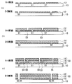
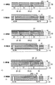
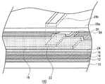
- FIG. 1 is a plan view of the photoelectric conversion device 100 as viewed from the back side opposite to the light receiving surface.
- 2, 3 and 4 are cross-sectional views for illustrating manufacturing steps along lines AA and BB in FIG.
- FIG. 5 is a perspective view for explaining the manufacturing process.
- the filler 28 and the back surface protective material 30 are not described, and components that are not actually seen overlapped are indicated by broken lines.
- the dimensions of each part are shown different from actual ones in order to clearly show the configuration.
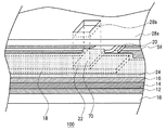
- the photoelectric conversion device 100 includes a substrate 10, a transparent electrode layer 12, a photoelectric conversion layer 14, a back electrode 16, a current collector wiring 18, an insulating member 20, an output wiring 22, and an insulating coating material 24. , The end sealing material 26, the filler 28, the back surface protection material 30, and the terminal box 32.
- the substrate 10 is a member that supports the photoelectric conversion device 100. Since the photoelectric conversion device 100 is configured to generate light by making light incident from the substrate 10 side, the substrate 10 is made of a material having transparency in at least a visible light wavelength region, such as a glass substrate or a plastic substrate. In the present embodiment, the substrate 10 made of glass is used.
- the transparent electrode layer 12 is formed on the substrate 10.
- the transparent electrode layer 12 is doped with tin oxide (SnO 2 ), zinc oxide (ZnO), indium tin oxide (ITO), etc. with tin (Sn), antimony (Sb), fluorine (F), aluminum (Al), etc. It is preferable to use at least one or a combination of a plurality of transparent conductive oxides (TCO).
- TCO transparent conductive oxide
- zinc oxide (ZnO) is preferable because it has high translucency, low resistivity, and excellent plasma resistance. Therefore, in the present embodiment, zinc oxide is used as the transparent electrode layer 12.
- the transparent electrode layer 12 can be formed by a sputtering method or a CVD method.
- the transparent electrode layer 12 is patterned in strip shape.
- the first slit S1 is formed and divided in the transparent electrode layer 12 along the vertical direction of FIG.
- the transparent electrode layer 12 is divided
- the second slit S2 is formed and divided in the transparent electrode layer 12 along the left-right direction in FIG.
- the transparent electrode layer 12 can be patterned using a YAG laser having a wavelength of 1064 nm, an energy density of 13 J / cm 2 , and a pulse frequency of 3 kHz.
- a p-type layer, an i-type layer, and an n-type silicon thin film are sequentially laminated on the transparent electrode layer 12 to form a photoelectric conversion layer 14.
- the photoelectric conversion layer 14 can be a thin film photoelectric conversion layer such as an amorphous silicon thin film photoelectric conversion layer or a microcrystalline silicon thin film photoelectric conversion layer. Alternatively, a tandem or triple photoelectric conversion layer in which these photoelectric conversion layers are stacked may be used.
- Amorphous silicon thin film photoelectric conversion layer and microcrystalline silicon thin film photoelectric conversion layer are made of silicon-containing gas such as silane (SiH 4 ), disilane (Si 2 H 6 ), dichlorosilane (SiH 2 Cl 2 ), diborane (B 2 H 6 ).
- a plasma chemical vapor deposition method in which a film is formed by converting a mixed gas obtained by mixing a p-type dopant-containing gas such as phosphine (PH 3 ) and an n-type dopant-containing gas such as phosphine (PH 3 ) and a diluent gas such as hydrogen (H 2 ) into a plasma (CVD method).
- a 13.56 MHz parallel plate RF plasma CVD method is preferably applied.
- the photoelectric conversion layer 14 is patterned into a strip shape.
- the YAG laser is irradiated to a position 50 ⁇ m lateral from the first slit S1 that divides the transparent electrode layer 12 to form a third slit S3, and the photoelectric conversion layer 14 is patterned into a strip shape.
- a YAG laser having an energy density of 0.7 J / cm 2 and a pulse frequency of 3 kHz is preferably used.
- the back electrode 16 is formed on the photoelectric conversion layer 14.
- the back electrode 16 may be a single layer or a laminate having conductivity, and preferably has a structure in which a transparent conductive oxide and a reflective metal are laminated in this order.
- transparent conductive oxide transparent conductive oxides such as tin oxide, zinc oxide and indium tin oxide, or those doped with impurities are used.
- zinc oxide doped with aluminum as an impurity may be used.
- a reflective metal metals, such as silver (Ag) and aluminum (Al), are used.
- the transparent conductive oxide and the reflective metal can be formed by, for example, a sputtering method or a CVD method. It is preferable that at least one of the transparent conductive oxide and the reflective metal is provided with unevenness for enhancing the light confinement effect.
- the back electrode 16 is made of silver oxide laminated on zinc oxide.
- the back surface electrode 16 is patterned in strip shape.
- a YAG laser is irradiated to a position 50 ⁇ m lateral from the position of the third slit S3 dividing the photoelectric conversion layer 14 to form a fourth slit S4, and the back electrode 16 is patterned into a strip shape.
- the 5th slit S5 which divides
- a YAG laser having an energy density of 0.7 J / cm 2 and a pulse frequency of 4 kHz is preferably used.
- the transparent electrode layer 12, the photoelectric conversion layer 14, and the back electrode 16 are stacked on the substrate 10 to form a plurality of photoelectric conversion cells 50.
- the current collecting wiring 18 is extended on the back electrode 16 of the photoelectric conversion cell 50 located at the end of the substrate 10.
- the current collector wiring 18 is formed to connect the positive electrodes and the negative electrodes of the photoelectric conversion layer 14 that are divided in parallel near the end of the photoelectric conversion device 100. Therefore, the current collection wiring 18 is extended along the extending direction of 1st slit S1. That is, the photoelectric conversion cells 50 divided in parallel by the second slit S2 and the fifth slit S5 are extended on the back electrode 16 across the second slit S2 and the fifth slit S5 so as to be connected in parallel. .
- the current collection wiring 18 is extended along the up-down direction in the left-right edge in FIG.
- the photoelectric conversion cell 50 having no photoelectric conversion function does not straddle the second slit S2 and the fifth slit S5 in the vicinity of the edge.
- the current collecting wiring 18 is electrically connected to the back electrode 16 by solder or the like melted by ultrasonic waves. Thereby, the positive electrodes and the negative electrodes of the photoelectric conversion cells 50 connected in series are connected in parallel.
- the insulating member 20 is moved from the vicinity of the current collector wiring 18 provided along the edge of the photoelectric conversion device 100 to the position of the terminal box 32 in the center. It extends along the extending direction of the second slit S2 on the back electrode 16 across the four slits S4.
- the insulating member 20 extends in the left-right direction from the vicinity of the left and right current collecting wires 18 toward the terminal box 32.
- the insulating member 20 is preferably composed of an insulating material having a resistivity of 10 16 ( ⁇ cm) or more.
- an insulating material having a resistivity of 10 16 ( ⁇ cm) or more.
- PET polyethylene terephthalate
- PEN polyethylene naphthalate
- PI polyimide
- PVF polyvinyl fluoride
- the output wiring 22 is arranged at the center of the photoelectric conversion device 100 along the extending direction of the second slit S 2 from the current collecting wiring 18 at both ends to the insulating member 20. It extends toward.
- the insulating member 20 is sandwiched between the output wiring 22 and the back electrode 16, and electrical insulation between the output wiring 22 and the back electrode 16 is maintained.
- One end of the output wiring 22 extends to the current collecting wiring 18 and is electrically connected to the current collecting wiring 18.
- the output wiring 22 is preferably electrically connected to the current collecting wiring 18 by solder or the like melted by ultrasonic waves.
- the other end of the output wiring 22 is connected to an electrode terminal in a terminal box 32 described later. Thereby, the electric power generated by the photoelectric conversion cell 50 is taken out of the photoelectric conversion device 100.
- the insulating coating material 24 includes at least the transparent electrode layer 12, the photoelectric conversion layer 14, the back electrode 16, and the current collector wiring 18 positioned in the vicinity of the end sealing material 26 described later. And provided so as to cover a part of the output wiring 22.
- the transparent electrode layer 12, the photoelectric conversion layer 14, the back electrode 16, the current collector wiring 18, and the output wiring 22 are preferably provided so as to cover the end surfaces.
- the insulating coating material 24 covers the first slits S ⁇ b> 1 of the photoelectric conversion layer 14 so as to cover the ends of the transparent electrode layer 12, the photoelectric conversion layer 14, the back electrode 16, the current collector wiring 18 and the output wiring 22. It extends along the extending direction. Specifically, in the area where the output wiring 22 is not provided, the entire surface of the current collecting wiring 18 and the ends of the transparent electrode layer 12, the photoelectric conversion layer 14, and the back electrode 16 are covered, and the output wiring 22 is provided. In the region, the insulating coating material 24 is disposed so as to cover a part of the surface of the output wiring 22 and the ends of the transparent electrode layer 12, the photoelectric conversion layer 14, and the back electrode 16.
- the insulating coating material 24 is preferably composed of an insulating material having a resistivity of 10 16 ( ⁇ cm) or more.
- an insulating material having a resistivity of 10 16 ( ⁇ cm) or more For example, PE, PET, PEN, PI, PVF and the like are preferable.
- the insulating coating material 24 has a tape shape, a sheet shape, or a film shape, and has a back surface coated with an adhesive in a seal shape. Thereby, the trouble at the time of arrange
- an end sealant 26 is disposed as shown in FIG.
- the end sealant 26 is disposed in a portion (width of about 7 mm to 15 mm) around the end of the photoelectric conversion device 100 where the photoelectric conversion cell 50 is not formed.
- the transparent electrode layer 12, the photoelectric conversion layer 14, and the back electrode 16 are not formed when the photoelectric conversion cell 50 is formed.
- a film forming process may be performed by masking the periphery of the substrate 10 using a frame member, or after the photoelectric conversion cell 50 is formed, the photoelectric conversion cell 50 around the end of the photoelectric conversion device 100 by laser, sandblasting or etching. May be removed.
- the end sealant 26 is provided by applying it to a portion where the photoelectric conversion cell 50 around the end of the photoelectric conversion device 100 thus formed is not formed.
- the end sealing material 26 is an insulating material having a resistivity of 10 10 ( ⁇ cm) or more.
- the end sealing material 26 is preferably made of a material having low moisture permeability in order to prevent moisture from entering from the end of the photoelectric conversion device 100.
- the end sealant 26 is preferably made of a material having a lower moisture permeability than the filler 28 described later.
- the end sealing material 26 is preferably an epoxy resin or a butyl resin, and more specifically, hot melt butyl that is easy to apply and adhere at high temperatures is preferably applied. is there.
- hot melt butyl is used as the end sealing material 26.
- the end sealing material 26 has a width of about 6 mm to 10 mm and a thickness of about 0.05 mm to 0.2 mm thicker than the thickness of the filler 28.
- the back surface protection material 30 is preferably made of a material having electrical insulation, low moisture permeability, and high corrosion resistance, and the back surface protection material 30 is made of glass. .
- a filler 28 is filled between the photoelectric conversion layer 14 and the back surface protective material 30, and the back surface of the photoelectric conversion device 100 is sealed with the back surface protective material 30.
- the filler 28 is an insulating material. More specifically, an insulating resin having a resistivity of about 10 14 ( ⁇ cm) is preferable. For example, ethylene vinyl acetate copolymer resin (EVA) or polyvinyl bratil (PVB) is preferable. In the present embodiment, EVA is used as the filler 28.
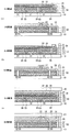
- the filler 28 for filling and sealing between the photoelectric conversion layer 14 and the back surface protective material 30 is formed of a resin sheet 28a.
- the area surrounded by the end sealing material 26 on the back surface of the photoelectric conversion device 100 is equal to the area surrounded by the end sealing material 26, or 1 mm smaller in length and width than the area.
- the resin sheet 28a is disposed.
- the resin sheet 28a from which the region overlapping the convex portion 70 formed by overlapping the current collecting wiring 18 and the output wiring 22 is removed is used.
- the resin sheet 28a in which the hole 28b is provided in the region overlapping the convex portion 70 is used.
- a resin sheet having a thickness of about 400 ⁇ m to 1 mm can be used, and in this embodiment, a resin sheet having a thickness of 600 ⁇ m is used.
- a back surface protection material A vacuum laminating process is performed by applying pressure from the 30 side. Furthermore, when EVA is used as the filler 28, the photoelectric conversion device 100 is heated to perform crosslinking. The heat treatment for crosslinking is preferably performed at 150 ° C. for about 30 minutes, for example.
- a photoelectric conversion layer is formed from the surroundings by adopting a structure in which the plurality of photoelectric conversion cells 50 are sealed by the substrate 10, the end sealing material 26 and the back surface protection material 30 as shown in FIG. It is possible to prevent moisture and corrosive substances from entering 14, and to improve the environmental resistance of the photoelectric conversion device 100.
- a terminal box 32 is attached in the vicinity of the end portion of the output wiring 22 drawn out from the back surface protective material 30 that protects the photoelectric conversion device 100.
- the terminal box 32 can be attached by bonding using silicone or the like.
- the end of the output wiring 22 is electrically connected to the terminal electrode in the terminal box 32 by soldering or the like, and the space in the terminal box 32 is filled with an insulating resin such as silicone and covered.
- the photoelectric conversion device 100 As described above, the photoelectric conversion device 100 according to the present embodiment is completed.
- the region corresponding to the convex portion 70 formed by overlapping the current collecting wiring 18 and the output wiring 22 is cut out, and the resin sheet 28a provided with the hole 28b is removed.
- the pressure is applied from the back surface protective material 30 side to the substrate 10 side and the vacuum laminating process is performed, the force concentrates in the vicinity of the convex portion 70 and the back surface protective material 30 is distorted and damaged, resulting in a low yield. Can be suppressed.
- the hole 28b provided in the resin sheet 28a is formed to have an area equal to or smaller than the area of the convex portion 70.
- the resin sheet 28a in the vicinity of the hole 28b melts during the heat treatment, enters between the convex portion 70 and the back surface protective material 30, and is better prevented from forming a space in the photoelectric conversion device 100 by being filled. can do. Therefore, it is possible to prevent moisture generated from water vapor that has penetrated through the filler 28 from entering the space formed in the photoelectric conversion device 100 and the weather resistance from being deteriorated. That is, by providing the resin sheet 28a with the holes 28b having an area equal to or smaller than the area of the convex portion 70, it is possible to simultaneously suppress the yield and the weather resistance from being lowered.
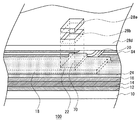
- the resin sheet 28a provided with the hole 28b in the region corresponding to the convex portion 70 formed by overlapping the current collecting wiring 18 and the output wiring 22 is used.
- a resin sheet 28 a provided with a hole 28 c corresponding to a region overlapping with the output wiring 22 as shown in FIG. 6 may be used.
- the insulating member 20 and the output wiring 22 are arranged so as to overlap with each other, and since it is convex with respect to the substrate surface, it is easy to concentrate force in the vicinity of this convex part. .
- one end of the output wiring 22 is connected to the terminal box 32 via an opening provided in the back surface protection member 30, the convex portion is formed up to a position where the opening overlaps.
- a hole 28 c is provided in the region of the resin sheet 28 a corresponding to the region overlapping with the output wiring 22.
- a resin sheet provided with holes in a region corresponding to a region overlapping with a convex portion formed on the substrate 10 as in the above-described embodiment may be used.
- the force concentrated on the back surface protective material 30 in the vicinity of the convex portion is dispersed, and it can be suppressed that the yield is lowered due to breakage.
- the resin sheet 28a having the holes 28b and 28c is used.
- the present invention is not limited to this, and a recess may be formed instead of the holes 28b and 28c. Even in this case, the same effect can be obtained.
- a resin sheet 28d having a high crosslinking speed in which holes 28b are formed and a resin sheet 28e made of a material having a low crosslinking speed may be used.
- the resin sheet 28e is disposed in the hole 28b of the resin sheet 28d.
- the cross-linking speed of the resin sheet 28e corresponding to the region overlapping with the convex portion 70 is slower than the resin sheet 28d in the region not overlapping with the convex portion 70 formed on the substrate 10, so that it does not overlap with the convex portion 70. Even if the region is cross-linked and hardened, the region overlapping the convex portion 70 can be made soft.
- the resin sheet 28e is deformed according to the shape of the convex portion 70, when the photoelectric conversion device 100 is formed by applying pressure from the back surface protective material 30 side to the substrate 10 side, stress inside the photoelectric conversion device 100 is applied. It can be mitigated, and it can be prevented from being broken and the yield is lowered. Further, the EVA constituting the resin sheet 28e is softened, and it is better prevented that a space is formed between the photoelectric conversion cell 50 and the back surface protective material 30 by entering and filling between the convex portion 70 and the back surface protective material 30. can do. As a result, it is possible to prevent moisture generated from water vapor that has permeated through the filler 28 from being accumulated in the space formed between the photoelectric conversion cell 50 and the back surface protective material 30, thereby reducing the weather resistance. .
- the resin sheet 28e corresponding to the region that does not overlap with the convex portion 70 may be cross-linked so that the photoelectric conversion device 100 has the required strength, and the resin sheet 28d corresponding to the region overlapping with the convex portion 70 is also used. It is not necessary to completely crosslink.
- the resin sheet 28d it is preferable to use EVA containing a reaction accelerator that increases the crosslinking rate.
- the resin sheet 28e the same EVA or the like as the resin sheet 28a is used, and is preferably about 1 to 5 mm larger than the convex portion 70. The thickness depends on the thickness of the convex portion 70. Thus, it is preferable to make it thinner than the resin sheet 28d.
- the resin sheet 28e having a low crosslinking speed is disposed in the hole 28b of the resin sheet 28d having a high crosslinking speed, but the present invention is not limited to this.
- the resin sheet 28f is made of a resin having a high crosslinking speed, and the resin sheet 28g is crosslinked.
- crosslinking speed such as what consists of resin with a slow speed
- the photoelectric conversion layer 14 has a pin junction, but the present invention is not limited to this and may have a pn junction as a basic structure. Further, the photoelectric conversion layer 14 is not only a silicon-based photoelectric conversion layer as in the above-described embodiments, but also, for example, cadmium tellurium, CIS (copper, indium, selenium), CIGS (copper, indium, gallium, selenium), or the like. A non-silicon photoelectric conversion layer can be used.
- the current collector wiring 18 is formed in the photoelectric conversion cells 50 at both ends.
- the position of the current collector wiring 18 is not limited to the photoelectric conversion cells 50 at both ends.
- Photoelectric conversion cell 70 170 Convex part 100, 200 Photoelectric conversion device
- the present invention can be used in a method for manufacturing a photoelectric conversion device such as a solar cell.
Landscapes
- Engineering & Computer Science (AREA)
- Life Sciences & Earth Sciences (AREA)
- Sustainable Development (AREA)
- Physics & Mathematics (AREA)
- Condensed Matter Physics & Semiconductors (AREA)
- Electromagnetism (AREA)
- General Physics & Mathematics (AREA)
- Computer Hardware Design (AREA)
- Microelectronics & Electronic Packaging (AREA)
- Power Engineering (AREA)
- Sustainable Energy (AREA)
- Photovoltaic Devices (AREA)
Abstract
光電変換装置100の製造方法は、基板10上に複数の光電変換セル50を形成する工程と、基板10上の複数の光電変換セル50を挟むように充填材28を介して裏面保護材30を接着する工程と、を有し、裏面保護材30を接着する工程においては、基板10の複数の光電変換セル50が形成された面に形成された凸部と重畳する領域を除去した樹脂シート28aを用いて充填材28を形成する。
Description
本発明は、光電変換装置の製造方法に関する。
太陽光を利用した発電システムとして、アモルファスや微結晶等の半導体薄膜を積層した光電変換装置が用いられている。
図9に示すように光電変換装置200は、ガラス基板110上に透明電極層112、光電変換層114、裏面電極116が形成され、複数の光電変換セル150が形成される。ガラス基板110の端部に位置する裏面電極116には、発電した電力を集電するために集電配線118が接続される。そして、集電配線に118は出力配線122が接続され、発電した電力が外部へ出力されている。
ガラス基板110に形成された光電変換セル150上には、集電配線118、絶縁部材120および出力配線122を光電変換セル150と裏面保護材130との間に封止するための充填材128(EVA)を配置し、光電変換装置200が形成される。
上記の光電変換装置200においては、裏面保護材130としてPET等の樹脂からなる単層体や、これによって金属箔を挟んだ積層体が用いられる。これらの樹脂等からなる単層体や積層体は、構造体としての役割を果たさない。そこで、光電変換装置200の周囲にアルミ等からなるフレームを構造部材として取り付けることにより、光電変換装置200の強度を高める。
しかしながら、このアルミ等からなるフレームを設けることにより、光電変換装置200のコストが高くなるため、フレームを設けることなく、裏面保護材130にガラスを用いて構造体としての役割を併せ持たせることが提案されている。
光電変換装置200において、集電配線118および出力配線122が重畳するように接続されるため、ガラス基板110上に凸部170が形成される。裏面保護材130としてガラスを用いる場合、樹脂等とは異なって、この凹凸に応じて柔軟に変形しない。このため、モジュールを形成する際に行われる真空ラミネート処理で裏面保護材130側からガラス基板110に圧力を加えたとき、凸部170近傍の裏面保護材130に力が集中し、裏面保護材130が歪み、割れが発生することがあり、歩留まりが低くなる問題がある。
本発明の光電変換装置の製造方法の1つの態様は、基板上の複数の光電変換セルを挟むように充填材を介して裏面保護材を接着する工程と、を有し、裏面保護材を接着する工程においては、基板の複数の光電変換セルが形成された面に形成された凸部と重畳する領域を除去した樹脂シートを用いて充填材を形成する。
本発明によれば、歩留まりの高い光電変換装置の製造方法を提供することができる。
図1~図5は、本発明の実施の形態における光電変換装置100の構成を示す。図1は、光電変換装置100を受光面とは反対側である裏面からみた平面図である。図2、図3および図4は、図1のラインA-AおよびB-Bに沿った製造工程を示すための断面図である。図5は、製造工程を説明するための斜視図である。なお、図1では、光電変換装置100の構成を明確に示すために充填材28および裏面保護材30を記載せず、実際には重なり合って見えない構成部分を破線で示している。また、図1~図5では、構成を明確に示すために各部の寸法を実際のものとは変えて示している。
光電変換装置100は、図1~図5に示すように、基板10、透明電極層12、光電変換層14、裏面電極16、集電配線18、絶縁部材20、出力配線22、絶縁被覆材24、端部封止材26、充填材28、裏面保護材30および端子ボックス32を含んで構成される。
基板10は、光電変換装置100を支持する部材である。光電変換装置100は基板10側から光を入射させて発電を行う構成であるので、基板10は、例えば、ガラス基板、プラスチック基板等の少なくとも可視光波長領域において透過性を有する材料を適用する。本実施の形態では、ガラスからなる基板10を用いた。
図2(a)に示すように基板10上に、透明電極層12を形成する。透明電極層12は、酸化錫(SnO2)、酸化亜鉛(ZnO)、インジウム錫酸化物(ITO)等に錫(Sn)、アンチモン(Sb)、フッ素(F)、アルミニウム(Al)等をドープした透明導電性酸化物(TCO)のうち少なくとも一種類又は複数種を組み合わせて用いることが好適である。特に、酸化亜鉛(ZnO)は、透光性が高く、抵抗率が低く、耐プラズマ特性にも優れているので好適である。そこで本実施の形態では、透明電極層12として酸化亜鉛を用いた。なお、透明電極層12はスパッタリング法又はCVD法で形成することができる。
光電変換セル50を複数直列に接続した構成とする場合、透明電極層12を短冊状にパターニングする。本実施の形態では、図1の上下方向に沿って透明電極層12に第1スリットS1を形成して分割する。また、光電変換セル50を並列に分割した構成とする場合、上記直列接続を形成するための第1スリットS1に直交する方向に短冊状にパターニングして透明電極層12を分割する。本実施の形態では、図1の左右方向に沿って透明電極層12に第2スリットS2を形成して分割する。例えば、波長1064nm、エネルギー密度13J/cm2、パルス周波数3kHzのYAGレーザを用いて透明電極層12をパターニングすることができる。
図2(b)に示すように透明電極層12上に、p型層、i型層、n型層のシリコン系薄膜を順に積層して光電変換層14を形成する。光電変換層14は、アモルファスシリコン薄膜光電変換層や微結晶シリコン薄膜光電変換層等の薄膜系光電変換層とすることができる。また、これらの光電変換層を積層したタンデム型やトリプル型の光電変換層としてもよい。
アモルファスシリコン薄膜光電変換層や微結晶シリコン薄膜光電変換層は、シラン(SiH4)、ジシラン(Si2H6)、ジクロルシラン(SiH2Cl2)等のシリコン含有ガス、ジボラン(B2H6)等のp型ドーパント含有ガス、フォスフィン(PH3)等のn型ドーパント含有ガスおよび水素(H2)等の希釈ガスを混合した混合ガスをプラズマ化して成膜を行うプラズマ化学気相成長法(CVD法)により形成することができる。プラズマCVD法は、例えば、13.56MHzの平行平板型RFプラズマCVD法を適用することが好適である。
複数の光電変換セル50を直列接続する場合、光電変換層14を短冊状にパターニングする。例えば、透明電極層12を分割する第1スリットS1から50μm横の位置にYAGレーザを照射して第3スリットS3を形成して光電変換層14を短冊状にパターニングする。YAGレーザは、例えば、エネルギー密度0.7J/cm2、パルス周波数3kHzのものを用いることが好適である。
図2(c)に示すように光電変換層14上に、裏面電極16を形成する。裏面電極16は、導電性を有する単層体或いは積層体を用いることができ、透明導電性酸化物と反射性金属とをこの順に積層した構造とすることが好適である。透明導電性酸化物としては、酸化錫、酸化亜鉛、インジウム錫酸化物等の透明導電性酸化物、又は、これらの透明導電性酸化物に不純物をドープしたものが用いられる。例えば、酸化亜鉛にアルミニウムを不純物としてドープしたものでもよい。また、反射性金属としては、銀(Ag)、アルミニウム(Al)等の金属が用いられる。透明導電性酸化物および反射性金属は、例えば、スパッタリング法又はCVD法等により形成することができる。透明導電性酸化物と反射性金属の少なくとも一方には、光閉じ込め効果を高めるための凹凸が設けることが好適である。本実施の形態では、裏面電極16として、酸化亜鉛上に反射金属として銀が積層されたものを用いた。
光電変換セル50を複数直列接続した構成とする場合、裏面電極16を短冊状にパターニングする。光電変換層14を分割する第3スリットS3の位置から50μm横の位置にYAGレーザを照射して第4スリットS4を形成して裏面電極16を短冊状にパターニングする。さらに、光電変換セル50を並列に分割した構成とする場合、透明電極層12を分割する第2スリットS2内に形成された光電変換層14および裏面電極16を分割する第5スリットS5を形成する。YAGレーザは、エネルギー密度0.7J/cm2、パルス周波数4kHzのものを用いることが好適である。
このように基板10上に透明電極層12、光電変換層14および裏面電極16を積層して複数の光電変換セル50が形成される。
続いて、図3(d)に示すように基板10端部に位置する光電変換セル50の裏面電極16上に集電配線18を延設する。集電配線18は、光電変換装置100の端辺付近において並列に分割された光電変換層14の正電極同士および負電極同士を接続するために形成する。したがって、集電配線18は、第1スリットS1の延在方向に沿って延設される。すなわち、第2スリットS2および第5スリットS5によって並列に分割された光電変換セル50を並列に接続するように、第2スリットS2および第5スリットS5を跨いで裏面電極16上に延設される。ここでは、集電配線18は、図1における左右の端辺に上下方向に沿って延設する。ただし、図1に示される上下の端辺近傍において、光電変換機能を有さない光電変換セル50と、その端辺近傍の第2スリットS2および第5スリットS5とは跨がない。集電配線18は、超音波で溶融したはんだ等によって裏面電極16に電気的に接続する。これによって、直列接続された光電変換セル50の正電極同士および負電極同士が並列に接続される。集電配線18としては、幅2mm、厚さ200μmを有するはんだで覆われた銅配線を用いる。
次に、図1および図3(e)に示すように、絶縁部材20を光電変換装置100の端辺に沿って設けられた集電配線18近傍から中央部の端子ボックス32の位置まで、第4スリットS4を跨いで裏面電極16上に第2スリットS2の延在方向に沿って延設する。ここでは、図1に示すように、絶縁部材20は、左右の集電配線18の近傍から端子ボックス32に向けて左右方向に沿って延設する。
絶縁部材20は、抵抗率が1016(Ωcm)以上の絶縁性の材料で構成することが好適である。例えば、ポリエステル(PE)、ポリエチレンテレフタラート(PET)、ポリエチレンナフタレート(PEN)、ポリイミド(PI)、ポリフッ化ビニル(PVF)等とすることが好適である。また、絶縁部材20は、テープ状、シート状、フィルム状の形状を有し、裏面にシール状に接着剤が塗布されたものを用いることが好適である。これにより、絶縁部材20を配設する際の手間が軽減される。そこで本実施の形態では、絶縁部材20としてPETテープを用いた。
出力配線22は、図1および図3(f)に示すように、両端の集電配線18上から絶縁部材20上へ第2スリットS2の延在方向に沿って、光電変換装置100の中央部へ向けて延設する。出力配線22と裏面電極16との間に絶縁部材20が挟み込まれ、出力配線22と裏面電極16との電気的な絶縁が保たれる。出力配線22の一端は集電配線18上まで延設され、集電配線18に電気的に接続される。例えば、出力配線22は超音波で溶融したはんだ等によって集電配線18に電気的に接続することが好適である。出力配線22の他端は、後述する端子ボックス32内の電極端子に接続される。これにより、光電変換セル50で発電された電力が光電変換装置100の外部へ取り出される。出力配線22としては、幅4mm、厚さ140μmを有するはんだで覆われた銅配線を用いた。
次に、図4(g)に示すように絶縁被覆材24は、少なくとも後述する端部封止材26の近傍に位置する透明電極層12、光電変換層14、裏面電極16、集電配線18および出力配線22の一部を覆うように設ける。特に、透明電極層12、光電変換層14、裏面電極16、集電配線18および出力配線22の端面を含んで覆うように設けることが好適である。
本実施の形態では、絶縁被覆材24は、透明電極層12、光電変換層14、裏面電極16、集電配線18および出力配線22の端部を覆うように光電変換層14の第1スリットS1の延在方向に沿って延設する。具体的には、出力配線22が設けられていない領域では集電配線18の表面全体並びに透明電極層12、光電変換層14および裏面電極16の端部を覆い、出力配線22が設けられている領域では出力配線22の表面の一部並びに透明電極層12、光電変換層14および裏面電極16の端部を覆うように絶縁被覆材24を配設する。
絶縁被覆材24は、抵抗率が1016(Ωcm)以上の絶縁性の材料で構成することが好適である。例えば、PE、PET、PEN、PI、PVF等とすることが好適である。また、絶縁被覆材24は、テープ状、シート状、フィルム状の形状を有し、裏面にシール状に接着剤が塗布されたものを用いることが好適である。これにより、絶縁被覆材24を配設する際の手間が軽減される。そこで本実施の形態では、絶縁被覆材24としてPETテープを用いた。
続いて、図4(h)に示すように端部封止材26を配設する。端部封止材26は、光電変換装置100の端部周辺の光電変換セル50を形成していない部分(幅7mm~15mm程度)に配設する。光電変換装置100の端部周辺において光電変換セル50を形成していない部分を設けるには、光電変換セル50を形成する際に透明電極層12、光電変換層14および裏面電極16が形成されないように枠部材を用いて基板10の周囲をマスクして成膜処理を行ってもよいし、光電変換セル50を形成後にレーザ、サンドブラスト又はエッチングによって光電変換装置100の端部周辺の光電変換セル50を除去してもよい。端部封止材26は、このようにして形成された光電変換装置100の端部周辺の光電変換セル50を形成していない部分に塗布することによって設ける。
端部封止材26は、抵抗率が1010(Ωcm)以上の絶縁材料とする。また、端部封止材26は、光電変換装置100の端部からの水分の浸入を防ぐために水分の透過性の低い材料とすることが好適である。特に、端部封止材26は、後述する充填材28よりも水分の透過性の低い材料とすることが好適である。さらに、光電変換装置100の端部に機械的な力が加えられた場合に、光電変換装置100に発生する力を緩和するための弾性を有することが好適である。例えば、端部封止材26は、エポキシ系樹脂やブチル系樹脂とすることが好適であり、より具体的には、高温での塗布および接着が容易なホットメルトブチルを適用することが好適である。そこで、本実施の形態では、端部封止材26としてホットメルトブチルを用いた。なお、端部封止材26は、その幅は6mm~10mm程度であり、厚さは充填材28の厚さよりも0.05mm~0.2mm程度厚くする。
端部封止材26を塗布した後、裏面保護材30によって光電変換装置100の裏面を封止する。裏面保護材30は、電気的な絶縁性を有し、水分の透過性が低く、耐腐食性が高い材料とすることが好適であり、裏面保護材30としては、ガラスからなるものが用いられる。光電変換層14と裏面保護材30との間には充填材28を充填して裏面保護材30により光電変換装置100の裏面を封止する。充填材28は、絶縁材料とする。より具体的には、抵抗率が1014(Ωcm)程度の絶縁樹脂とすることが好適であり、例えば、エチレン酢酸ビニル共重合樹脂(EVA)やポリビニルブラチール(PVB)とすることが好適であり、本実施の形態では充填材28としてEVAを用いた。
光電変換層14と裏面保護材30との間を充填し、封止するための充填材28は、樹脂シート28aにより形成する。図5に示すように、光電変換装置100の裏面の端部封止材26で囲まれた領域に端部封止材26で囲まれた領域と同等か、若しくはその領域よりも縦横ともに1mm小さい樹脂シート28aを配置する。このとき、集電配線18と出力配線22が重なって形成される凸部70に重畳する領域が除去された樹脂シート28aを用いる。具体的には本実施の形態では、凸部70に重畳する領域に孔28bが設けられた樹脂シート28aを用いた。また、樹脂シート28aとしては、厚さ400μm~1mm程度のものが用いることができ、本実施の形態では厚さ600μmのものを用いた。
そして、光電変換装置100の裏面を覆うように裏面保護材30を配置し、端子ボックス32へ出力配線22の端部を接続するために裏面保護材30から引き出す処理を施した後に、裏面保護材30側から圧力を加えて真空ラミネート処理を施す。さらに、充填材28としてEVAを用いた場合にあっては、光電変換装置100を加熱し、架橋を行う。架橋を行うための加熱処理は、例えば150℃で30分程度行うとよい。
このようにして、図4(i)に示すような基板10、端部封止材26および裏面保護材30によって複数の光電変換セル50を封止する構造とすることによって、周囲から光電変換層14への水分や腐食性物質が浸入することを防ぐことができ、光電変換装置100の耐環境性を高めることができる。
最後に、図1に示すように、光電変換装置100を保護する裏面保護材30から引き出された出力配線22の端部の近傍に端子ボックス32を取り付ける。端子ボックス32は、シリコーン等を用いて接着して取り付けることができる。出力配線22の端部を端子ボックス32内の端子電極にハンダ付け等により電気的に接続し、端子ボックス32内の空間にシリコーン等の絶縁樹脂を充填して蓋をする。
以上のようにして、本実施の形態における光電変換装置100が完成する。
本発明の実施形態においては、図5に示すように、集電配線18と出力配線22が重なって形成される凸部70に対応した領域は切り取られ、孔28bが設けられた樹脂シート28aを用いる。これによって、裏面保護材30側から基板10側へ圧力を加えて真空ラミネート処理を施したときに凸部70近傍に力が集中して裏面保護材30が歪み、破損して歩留まりが低くなることを抑制できる。
また樹脂シート28aに設けられた孔28bは、凸部70の面積以下の面積となるように形成される。これにより、孔28b近傍の樹脂シート28aが加熱処理の際に溶融し、凸部70と裏面保護材30の間に入り込み、充填されることによって光電変換装置100中に空間ができることをより良く防止することができる。したがって、光電変換装置100中にできた空間に、充填材28を透過して侵入した水蒸気から発生した水分が溜まり、耐候性が低下することを防止することができる。つまり、樹脂シート28aに凸部70以下の面積以下の面積の孔28bを設けるにより、歩留まりが低くなることと耐候性の低下を同時に抑制することができる。
なお、本実施の形態においては、集電配線18と出力配線22が重なって形成される凸部70に対応する領域に孔28bを設けた樹脂シート28aを用いたが、これに限らず他の実施の形態として、図6に示したように出力配線22と重畳する領域に対応する孔28cを設けた樹脂シート28aを用いてもよい。裏面電極16上には、絶縁部材20と出力配線22が重なるように配置された構成となっており、基板面に対して凸となっているため、この凸部近傍に力が集中し易かった。さらには、出力配線22の一方端は、裏面保護材30に設けられた開孔部を介して端子ボックス32に接続するため、凸部はこの開孔部が重畳する位置まで形成される。このため、裏面保護材30側から基板10側へ圧力を加えて真空ラミネート処理を施したときに開孔部を起点として裏面保護材30に亀裂が入り、破損することがあった。そこで、本発明の他の実施の形態では、出力配線22と重畳する領域に対応する樹脂シート28aの領域に孔28cを設ける。これにより、出力配線22近傍において裏面保護材30に集中する力が分散し、破損して歩留まりが低くなることを抑制することができる。
つまり、本発明においては上述の実施形態のように基板10上に形成された凸部と重畳する領域に対応する領域に孔を設けた樹脂シートを用いればよい。これにより、凸部近傍において裏面保護材30に集中する力が分散し、破損して歩留まりが低くなることを抑制することができる。
また、上記実施の形態では、樹脂シート28aに孔28b、28cを形成したものを用いたが、これに限らず、孔28b、28cの代わりに凹部を形成してもよい。この場合であっても、同様の作用効果を得ることができる。
さらには、図7に示すように孔28bを形成した架橋速度の速い樹脂シート28dと、架橋速度の遅い材料からなる樹脂シート28eを用いてもよい。具体的には、樹脂シート28dの孔28b内に樹脂シート28eを配置する。この結果、基板10上に形成された凸部70と重畳しない領域の樹脂シート28dに比べ、凸部70と重畳する領域に対応する樹脂シート28eの架橋速度が遅いため、凸部70と重畳しない領域を架橋して固くしても、凸部70と重畳する領域を柔らかい状態とすることができる。つまり、樹脂シート28eは、凸部70の形状に応じて変形するため、裏面保護材30側から基板10側へ圧力を加えて光電変換装置100を形成した時に光電変換装置100内部での応力を緩和し、破損して歩留まりが低くなることを抑制できる。また、樹脂シート28eを構成するEVAが柔らかくなり、凸部70と裏面保護材30の間に入り込み充填されることによって光電変換セル50と裏面保護材30との間に空間ができることをより良く防止することができる。これによって、光電変換セル50と裏面保護材30との間にできた空間に、充填材28を透過して侵入した水蒸気から発生した水分が溜まり、耐候性が低下することを防止することができる。
なお、少なくとも凸部70と重畳しない領域に対応する樹脂シート28eにおいて、光電変換装置100が必要とする強度となるように架橋すればよく、凸部70と重畳する領域に対応する樹脂シート28dも完全に架橋しなくても良い。
また、樹脂シート28dとしては、架橋速度を高める反応促進剤を含むEVAなどを用いることが好ましい。さらに樹脂シート28eとしては、樹脂シート28aと同様のEVAなどが用いられ、凸部70に比べて1~5mm程度大きい大きさとすることが好ましく、厚さについては、凸部70の厚さに応じて樹脂シート28dよりも薄くすることが好ましい。
また、本実施の形態では、架橋速度の速い樹脂シート28dの孔28b内に架橋速度の遅い樹脂シート28eを配置したが、これに限られない。例えば、図8の樹脂シートのように出力配線22と重畳する領域に対応する領域に孔28cを設けた場合にあっては、架橋速度の速い樹脂からなる樹脂シート28fとし、樹脂シート28gを架橋速度の遅い樹脂からなるものとするなど、架橋速度の速い樹脂シートに設けた孔の内部に架橋速度の遅い樹脂を配置すればよい。なお、同様の効果は、固い樹脂シートに設けた孔の内部に柔らかい樹脂シートを配置しても得ることができる。
上記各実施の形態では、光電変換層14はpin接合を有するものとしたが、これに限定されるものではなく、pn接合を基本構造とするものでもよい。さらに光電変換層14は、上記各実施の形態のようにシリコン系光電変換層の他、例えば、カドミウムテルルや、CIS(銅、インジウム、セレン)又はCIGS(銅、インジウム、ガリウム、セレン)系などの非シリコン系の光電変換層を用いることができる。
また、上記各実施の形態では、両端の光電変換セル50に集電配線18を形成したが、集電配線18の位置は両端の光電変換セル50に限られない。
10、110 基板
12、112 透明電極層
14、114 光電変換層
16、116 裏面電極
18、118 集電配線
20、120 絶縁部材
22、122 出力配線
24 絶縁被覆材
26 端部封止材
28、128 充填材
30、130 裏面保護材
32 端子ボックス
50、150 光電変換セル
70、170 凸部
100、200 光電変換装置
12、112 透明電極層
14、114 光電変換層
16、116 裏面電極
18、118 集電配線
20、120 絶縁部材
22、122 出力配線
24 絶縁被覆材
26 端部封止材
28、128 充填材
30、130 裏面保護材
32 端子ボックス
50、150 光電変換セル
70、170 凸部
100、200 光電変換装置
本発明は、太陽電池などの光電変換装置の製造方法に利用できる。
Claims (12)
- 基板上に複数の光電変換セルを形成する工程と、
前記基板上の前記複数の光電変換セルを挟むように充填材を介して裏面保護材を接着する工程と、
を有する光電変換装置の製造方法であって、
前記裏面保護材を接着する工程においては、前記基板の前記複数の光電変換セルが形成された面に形成された凸部と重畳する領域を除去した樹脂シートを用いて前記充填材を形成する
ことを特徴とする光電変換装置の製造方法。 - 請求項1に記載の光電変換装置の製造方法であって、
前記充填材は、前記凸部に重畳する領域以下の面積を除去した樹脂シートを用いることを特徴とする光電変換装置の製造方法。 - 請求項1に記載の光電変換装置の製造方法であって、
前記充填材は、前記凸部に対応した領域に孔を設けた樹脂シートを用いて形成することを特徴とする光電変換装置の製造方法。 - 請求項3に記載の光電変換装置の製造方法であって、
前記充填材は、前記凸部に重畳する領域以下の面積の孔を形成した樹脂シートを用いることを特徴とする光電変換装置の製造方法。 - 基板上に複数の光電変換セルを形成する工程と、
前記基板上の前記複数の光電変換セルを挟むように充填材を介して裏面保護材を接着する工程と、
を有する光電変換装置の製造方法であって、
前記裏面保護材を接着する工程において、前記充填材は、前記基板の前記複数の光電変換セルが形成された面に形成された凸部と重畳する領域が他の領域より架橋速度の遅い樹脂シートを用いて形成する
ことを特徴とする光電変換装置の製造方法。 - 請求項5に記載の光電変換装置の製造方法であって、
前記充填材は、前記凸部に重畳する領域に孔を形成した第1の樹脂シートを用い、前記孔内に前記第1の樹脂シートより架橋速度の遅い第2の樹脂シートを配置して形成することを特徴とする光電変換装置の製造方法。 - 基板上に複数の光電変換セルを形成する工程と、
前記基板上の前記複数の光電変換セルを挟むように充填材を介して裏面保護材を接着する工程と、
を有する光電変換装置の製造方法であって、
前記裏面保護材を接着する工程において、前記充填材は、前記基板の前記複数の光電変換セルが形成された面に形成された凸部と重畳する領域が他の領域より柔らかい樹脂シートを用いて形成する
ことを特徴とする光電変換装置の製造方法。 - 請求項7に記載の光電変換装置の製造方法であって、
前記充填材は、前記凸部に重畳する領域に孔を形成した第1の樹脂シートを用い、前記孔内に前記第1の樹脂シートより柔らかい第2の樹脂シートを配置して形成することを特徴とする光電変換装置の製造方法。 - 請求項1~8のいずれか1項に記載の光電変換装置の製造方法であって、
前記複数の光電変換セルに電流を集めるための集電配線を形成する工程と、
前記集電配線に電力を外部に出力するための出力配線を形成する工程と、
前記凸部は、前記集電配線と前記出力配線とが重畳する領域であることを特徴とする光電変換装置の製造方法。 - 請求項1~8のいずれか1項に記載の光電変換装置の製造方法であって、
前記複数の光電変換セルに電流を集めるための集電配線を形成する工程と、
前記集電配線に電力を外部に出力するための出力配線を形成する工程と、
前記凸部は、前記出力配線に重畳する領域であることを特徴とする光電変換装置の製造方法。 - 請求項9または10に記載の光電変換装置の製造方法であって、
前記光電変換セルおよび前記集電配線の前記基板端部側の端面を絶縁被覆材で覆うことを特徴とする光電変換装置の製造方法。 - 請求項1~11のいずれか1項に記載の光電変換装置の製造方法であって、
前記光電変換セルが形成されていない前記基板端部において、端部封止部材が形成されていることを特徴とする光電変換装置の製造方法。
Applications Claiming Priority (4)
| Application Number | Priority Date | Filing Date | Title |
|---|---|---|---|
| JP2010176575 | 2010-08-05 | ||
| JP2010-176575 | 2010-08-05 | ||
| JP2011075261A JP2013219066A (ja) | 2010-08-05 | 2011-03-30 | 光電変換装置の製造方法 |
| JP2011-075261 | 2011-03-30 |
Publications (1)
| Publication Number | Publication Date |
|---|---|
| WO2012017661A1 true WO2012017661A1 (ja) | 2012-02-09 |
Family
ID=45559180
Family Applications (1)
| Application Number | Title | Priority Date | Filing Date |
|---|---|---|---|
| PCT/JP2011/004424 WO2012017661A1 (ja) | 2010-08-05 | 2011-08-04 | 光電変換装置の製造方法 |
Country Status (2)
| Country | Link |
|---|---|
| JP (1) | JP2013219066A (ja) |
| WO (1) | WO2012017661A1 (ja) |
Citations (3)
| Publication number | Priority date | Publication date | Assignee | Title |
|---|---|---|---|---|
| JP2002151711A (ja) * | 2000-11-15 | 2002-05-24 | Kanegafuchi Chem Ind Co Ltd | 薄膜太陽電池の裏面封止方法 |
| JP2006128289A (ja) * | 2004-10-27 | 2006-05-18 | Sharp Corp | 接着樹脂フィルムおよび半導体モジュールの製造方法 |
| WO2009099180A1 (ja) * | 2008-02-06 | 2009-08-13 | Sanyo Electric Co., Ltd. | 太陽電池モジュール |
-
2011
- 2011-03-30 JP JP2011075261A patent/JP2013219066A/ja not_active Withdrawn
- 2011-08-04 WO PCT/JP2011/004424 patent/WO2012017661A1/ja active Application Filing
Patent Citations (3)
| Publication number | Priority date | Publication date | Assignee | Title |
|---|---|---|---|---|
| JP2002151711A (ja) * | 2000-11-15 | 2002-05-24 | Kanegafuchi Chem Ind Co Ltd | 薄膜太陽電池の裏面封止方法 |
| JP2006128289A (ja) * | 2004-10-27 | 2006-05-18 | Sharp Corp | 接着樹脂フィルムおよび半導体モジュールの製造方法 |
| WO2009099180A1 (ja) * | 2008-02-06 | 2009-08-13 | Sanyo Electric Co., Ltd. | 太陽電池モジュール |
Also Published As
| Publication number | Publication date |
|---|---|
| JP2013219066A (ja) | 2013-10-24 |
Similar Documents
| Publication | Publication Date | Title |
|---|---|---|
| WO2014002329A1 (ja) | 太陽電池モジュールおよびその製造方法 | |
| WO2012029651A1 (ja) | 光電変換装置及びその製造方法 | |
| JP2013077821A (ja) | 太陽電池モジュール | |
| WO2008038553A1 (en) | Solar cell module | |
| JP2010272725A (ja) | 薄膜太陽電池モジュールとその製造方法 | |
| JP5702472B2 (ja) | 合わせガラス構造太陽電池モジュール | |
| JP2019102620A (ja) | 太陽電池モジュール | |
| WO2009099180A1 (ja) | 太陽電池モジュール | |
| US20120090680A1 (en) | Solar cell module and method for manufacturing solar cell module | |
| JP2014120733A (ja) | 太陽電池モジュール、並びに、窓 | |
| US20190379321A1 (en) | Solar roof tile connectors | |
| WO2011148930A1 (ja) | 太陽電池モジュール及びその製造方法 | |
| JP2011210747A (ja) | 太陽電池モジュール及びその製造方法 | |
| US20120024339A1 (en) | Photovoltaic Module Including Transparent Sheet With Channel | |
| JP2010118705A (ja) | 太陽電池モジュール | |
| WO2014050193A1 (ja) | 光電変換モジュール | |
| WO2012023260A1 (ja) | 光電変換装置およびその製造方法 | |
| JP6025123B2 (ja) | 太陽電池モジュール | |
| WO2012017661A1 (ja) | 光電変換装置の製造方法 | |
| WO2011105167A1 (ja) | 光電変換装置 | |
| WO2011114781A1 (ja) | 光電変換装置およびその製造方法 | |
| WO2012029668A1 (ja) | 光電変換装置 | |
| US20110017260A1 (en) | Solar cell module | |
| JP4512650B2 (ja) | 太陽電池モジュールの製造方法 | |
| WO2012029657A1 (ja) | 光電変換装置及びその製造方法 |
Legal Events
| Date | Code | Title | Description |
|---|---|---|---|
| 121 | Ep: the epo has been informed by wipo that ep was designated in this application |
Ref document number: 11814296 Country of ref document: EP Kind code of ref document: A1 |
|
| NENP | Non-entry into the national phase |
Ref country code: DE |
|
| 122 | Ep: pct application non-entry in european phase |
Ref document number: 11814296 Country of ref document: EP Kind code of ref document: A1 |
|
| NENP | Non-entry into the national phase |
Ref country code: JP |