WO2012017532A1 - 半導体センサ - Google Patents
半導体センサ Download PDFInfo
- Publication number
- WO2012017532A1 WO2012017532A1 PCT/JP2010/063225 JP2010063225W WO2012017532A1 WO 2012017532 A1 WO2012017532 A1 WO 2012017532A1 JP 2010063225 W JP2010063225 W JP 2010063225W WO 2012017532 A1 WO2012017532 A1 WO 2012017532A1
- Authority
- WO
- WIPO (PCT)
- Prior art keywords
- electrode
- electric
- potential
- portions
- substrate
- Prior art date
- Legal status (The legal status is an assumption and is not a legal conclusion. Google has not performed a legal analysis and makes no representation as to the accuracy of the status listed.)
- Ceased
Links
Images


Classifications
-
- G—PHYSICS
- G01—MEASURING; TESTING
- G01N—INVESTIGATING OR ANALYSING MATERIALS BY DETERMINING THEIR CHEMICAL OR PHYSICAL PROPERTIES
- G01N25/00—Investigating or analyzing materials by the use of thermal means
- G01N25/56—Investigating or analyzing materials by the use of thermal means by investigating moisture content
- G01N25/66—Investigating or analyzing materials by the use of thermal means by investigating moisture content by investigating dew-point
-
- G—PHYSICS
- G01—MEASURING; TESTING
- G01L—MEASURING FORCE, STRESS, TORQUE, WORK, MECHANICAL POWER, MECHANICAL EFFICIENCY, OR FLUID PRESSURE
- G01L19/00—Details of, or accessories for, apparatus for measuring steady or quasi-steady pressure of a fluent medium insofar as such details or accessories are not special to particular types of pressure gauges
- G01L19/06—Means for preventing overload or deleterious influence of the measured medium on the measuring device or vice versa
- G01L19/0627—Protection against aggressive medium in general
- G01L19/0654—Protection against aggressive medium in general against moisture or humidity
-
- G—PHYSICS
- G01—MEASURING; TESTING
- G01L—MEASURING FORCE, STRESS, TORQUE, WORK, MECHANICAL POWER, MECHANICAL EFFICIENCY, OR FLUID PRESSURE
- G01L9/00—Measuring steady of quasi-steady pressure of fluid or fluent solid material by electric or magnetic pressure-sensitive elements; Transmitting or indicating the displacement of mechanical pressure-sensitive elements, used to measure the steady or quasi-steady pressure of a fluid or fluent solid material, by electric or magnetic means
- G01L9/0041—Transmitting or indicating the displacement of flexible diaphragms
- G01L9/0042—Constructional details associated with semiconductive diaphragm sensors, e.g. etching, or constructional details of non-semiconductive diaphragms
Definitions
- the present invention relates to a semiconductor sensor, and more particularly to a semiconductor sensor in which an electric circuit made of a metal thin film is formed on the surface of a semiconductor element.
- Patent Documents 1 to 4 semiconductor sensors used for automobile engine control, barometers, and the like are known (see, for example, Patent Documents 1 to 4).
- the semiconductor sensor described in Patent Document 1 includes a substrate having a diaphragm portion as a semiconductor sensor, and performs a failure diagnosis of the diaphragm portion based on a voltage change between the conductor and the diaphragm portion.
- the semiconductor sensor described in Patent Document 2 includes a bridge circuit made of a strain gauge as a semiconductor sensor, and performs a failure diagnosis that detects a disconnection of a wiring between the bridge circuit and a measuring instrument.
- the semiconductor sensor described in Patent Document 3 connects a wire to a wire bonding pad of a semiconductor element, detects whether or not a current flows from the wire to the wire bonding pad, and causes a failure due to the life of the semiconductor element in advance. Predict the failure to be detected.
- the semiconductor sensor described in Patent Document 4 is provided with a failure prediction element that has a deterioration progress faster than a normal element on a semiconductor substrate, and detects the degree of deterioration of the deterioration prediction element to predict the occurrence of a deterioration failure. I do.
- semiconductor elements are mounted in a casing.
- condensation may occur on the surface of the semiconductor element as the temperature changes. If dew condensation occurs on the surface of the semiconductor element, electrolytic corrosion may occur in the electrode part and the electric conductor part, and electrical conduction may be interrupted.
- electrical continuity is interrupted in a semiconductor element, the semiconductor element does not drive normally, and as a result, the semiconductor sensor does not operate normally until the semiconductor element is repaired or replaced. Therefore, in order to always maintain the normal driving of the semiconductor element, before the semiconductor element breaks down, specifically, before the semiconductor element shifts from a normal driving state to a non-driving state due to condensation. It is necessary to detect dew condensation generated on the surface of the semiconductor element.
- the conventional semiconductor sensor for example, the techniques of Patent Documents 1 to 4
- the present invention has been made in view of the above points, and an object of the present invention is to provide a semiconductor sensor capable of detecting condensation occurring on the surface of a semiconductor element before the occurrence of a failure due to condensation of the semiconductor element. To do.
- the semiconductor sensor of the present invention is a semiconductor sensor in which an electric circuit made of a metal thin film is formed on the surface of a semiconductor element, and is disposed as opposed to each other on the surface of the semiconductor element as a part of the electric circuit.
- the separation distance between the two electric conductor portions is smaller than the minimum distance of the distances between any two electrode portions or electric conductor portions of the electric circuit excluding the separation distance. Is preferably small.
- the high potential electrical conductor portion to which a high potential is applied among the two electrical conductor portions is applied with the low potential of the two electrical conductor portions on the surface of the semiconductor element. It is preferable to arrange between the low-potential electric conductor part and the electrode part or other electric conductor part of the electric circuit.
- the shape of the two electric conductor portions on the surface of the semiconductor element is a shape that easily collects condensed moisture.
- a first resistor connected in parallel to one of the two electric conductor portions, and a first resistor connected to the one electric conductor portion and the first resistor.
- a first electrode connected to one end of the first resistor, a second resistor having one end connected to the other end of the one electrical conductor and the first resistor, and the other of the two electrical conductors
- a constant current is circulated between the second electrode portion connected to the electric conductor and the other end of the second resistor, and between the first electrode portion and the second electrode portion.
- the dew detection circuit includes the first electrode in a situation where a constant current is circulated between the first electrode part and the second electrode part by the constant current circulation means.
- a second electrode part connected to the other electric conductor part of the electric conductor parts and connected to the other end of the resistor is fixed between the first electrode part and the second electrode part.
- a constant voltage application means for applying a voltage, and the dew condensation detection circuit is configured to apply a constant voltage between the first electrode portion and the second electrode portion by the constant voltage application means. It is preferable to determine that dew condensation has occurred on the surface of the semiconductor element when the potential difference generated between the two electric conductor portions does not reach the vicinity of the constant voltage.
- each of the two electric conductor portions is mainly made of aluminum.
- the two electric conducting wire portions are disposed on the outer peripheral side of a diaphragm formed on the surface of the semiconductor element.
- the present invention it is possible to detect the dew condensation that has occurred on the surface of the semiconductor element before the failure due to the dew condensation of the semiconductor element.
- FIG. 1 is a top view of a semiconductor sensor according to a first embodiment of the present invention. It is a circuit block diagram of the failure prediction circuit in the semiconductor sensor which concerns on 1st Embodiment of this invention. It is a flowchart of an example of the control routine which a failure prediction circuit performs in the semiconductor sensor which concerns on 1st Embodiment of this invention. It is a top view of the semiconductor sensor which concerns on 2nd Embodiment of this invention. It is a flowchart of an example of the control routine which a failure prediction circuit performs in the semiconductor sensor which concerns on 2nd Embodiment of this invention. It is a top view of the semiconductor sensor which concerns on the modification of this invention. (A)-(g) is a partial top view which shows the shape of an electrically-conductive wire part in the semiconductor sensor which concerns on embodiment of this invention.
- a semiconductor sensor is a semiconductor sensor in which an electric circuit made of a metal thin film is formed on the surface of a semiconductor element, and is disposed to face each other on the surface of the semiconductor element as a part of the electric circuit Two electrical conductor portions to which different potentials are applied, and a dew condensation detection circuit that determines whether or not condensation has occurred on the surface of the semiconductor element based on a potential difference generated in the two electrical conductor portions. It is a semiconductor sensor provided.
- an electric circuit made of a metal thin film formed on the surface of a semiconductor element has two electric circuits that are arranged opposite to each other on the surface of the semiconductor element and to which different potentials are applied. It has a conductor part.
- the metal thin film for example, aluminum
- the metal thin film of the two opposing electrical conductor portions melts from the high potential side, and electrolytic corrosion occurs. Is generated, and the metal thin film on the high potential side is cut, whereby electrical conduction is interrupted.
- the separation distance between the two electric conductor portions is smaller than the minimum distance of the distances between any two electrode portions or electric conductor portions of the electric circuit excluding the separation distance. Is preferably small.
- the separation distance between two electric conductor portions that are arranged opposite to each other on the surface of the semiconductor element and to which different electric potentials are applied is equal to any two electrode portions or electric conductor portions of the electric circuit. It is smaller than the minimum distance of the distance between them excluding the separation distance. For this reason, when condensation occurs on the surface of a semiconductor element, the part where moisture accompanying the condensation easily adheres, that is, the part where the electrolytic corrosion due to condensation occurs at the earliest timing is all of the electrode part and the electric conductor part on the semiconductor element. Among these combinations, it is considered that the two electric conductive wire portions are arranged opposite to each other on the surface of the semiconductor element and are applied with different potentials.
- the high potential electrical conductor portion to which a high potential is applied among the two electrical conductor portions is applied with the low potential of the two electrical conductor portions on the surface of the semiconductor element. It is preferable to arrange between the low-potential electric conductor part and the electrode part or other electric conductor part of the electric circuit.
- the high-potential electrical conductor portion of the two electrical conductor portions that are arranged opposite to each other on the surface of the semiconductor element and to which different potentials are applied is the low-potential electrical conductor portion and the electrical circuit electrode portion or It arrange
- electrolytic corrosion due to condensation of a semiconductor element occurs on the high potential side. For this reason, even when the potential of the low-potential electrical lead portion is lower than the potential of the electrode portion or electrical lead portion other than the high-potential electrical lead portion, dew condensation occurs between the high-potential electrical lead portion and the low-potential electrical lead portion.
- the shape of the two electric conductor portions on the surface of the semiconductor element is a shape that easily collects condensed moisture.
- the shape of the two electric conducting wire portions that are arranged opposite to each other on the surface of the semiconductor element and to which different potentials are applied is a shape that easily collects condensed moisture. For this reason, it becomes easy to detect the dew condensation generated on the surface of the semiconductor element before the occurrence of the failure due to the dew condensation of the semiconductor element.
- a first resistor connected in parallel to one of the two electric conductor portions, and a first resistor connected to the one electric conductor portion and the first resistor.
- a first electrode connected to one end of the first resistor, a second resistor having one end connected to the other end of the one electrical conductor and the first resistor, and the other of the two electrical conductors
- a constant current is circulated between the second electrode portion connected to the electric conductor and the other end of the second resistor, and between the first electrode portion and the second electrode portion.
- the dew detection circuit includes the first electrode in a situation where a constant current is circulated between the first electrode part and the second electrode part by the constant current circulation means.
- the flowing current when a constant current flows between the first electrode portion and the second electrode portion, when the electrical continuity of one electric conductor portion is maintained, the flowing current is mainly one of them. Therefore, the potential difference between the first electrode portion and the second electrode portion is relatively small.
- the electrical continuity of one of the electrical conducting wire portions is interrupted, the flowing current mainly flows through the first resistance side, so that the potential difference between the first electrode portion and the second electrode portion is relatively small. growing. Therefore, if it is determined that condensation has occurred on the surface of the semiconductor element when the potential difference between the first electrode portion and the second electrode portion is relatively large, the presence or absence of the condensation can be accurately detected. It becomes easy to do.
- a second electrode part connected to the other electric conductor part of the electric conductor parts and connected to the other end of the resistor is fixed between the first electrode part and the second electrode part.
- a constant voltage application means for applying a voltage, and the dew condensation detection circuit is configured to apply a constant voltage between the first electrode portion and the second electrode portion by the constant voltage application means. It is preferable to determine that dew condensation has occurred on the surface of the semiconductor element when the potential difference generated between the two electric conductor portions does not reach the vicinity of the constant voltage.
- each of the two electric conductor portions is mainly made of aluminum.
- the two electric conducting wire portions are disposed on the outer peripheral side of a diaphragm formed on the surface of the semiconductor element.
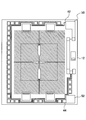
- FIG. 1 shows a top view of a semiconductor sensor 10 according to a first embodiment of the present invention.
- the semiconductor sensor 10 of the present embodiment is a pressure sensor used for automobile engine control, exhaust purification control, or a barometer.
- the semiconductor sensor 10 can be used, for example, to detect pressure in an exhaust path through which exhaust gas discharged from an internal combustion engine flows. Further, the semiconductor sensor 10 can be used for detecting a pressure difference between an upstream side and a downstream side of a filter installed in the exhaust path. Furthermore, the semiconductor sensor 10 can be used as a particulate quantity detection sensor that detects the particulate quantity deposited on the filter based on the pressure difference between the upstream side and the downstream side of the filter installed in the exhaust path.
- the semiconductor sensor 10 includes a silicon (Si) substrate 12 as a semiconductor element.
- the semiconductor sensor 10 is manufactured by applying a known semiconductor manufacturing technique to the Si substrate 12.
- the Si substrate 12 is a planar substantially rectangular plate-like member partitioned by four sides.
- an opening 14 (a portion surrounded by a broken line in FIG. 1) is formed in a concave shape on the main back surface.
- the opening 14 is formed by anisotropically etching the Si substrate 12.
- the opening 14 forms a space surrounded by four diaphragm side walls.
- a thin (thin plate) diaphragm 16 is formed on the main surface side of the opening 14.
- the opening 14 and the diaphragm 16 are disposed at the approximate center of the surface of the Si substrate 12.
- the diaphragm 16 is a thin member that can be bent by an amount corresponding to the pressure difference between the front and back sides.
- the planar shape of the diaphragm 16 is a rectangular shape that is a substantially square surrounded by two pairs of sides facing each other in parallel.
- the diaphragm 16 is formed as the opening 14 is formed by anisotropically etching the Si substrate 12.
- the electric circuit 18 is composed of an impurity layer made of boron or phosphorus, or a metal thin film layer made of aluminum or the like.
- the impurity layer of the electric circuit 18 is formed inside the Si substrate 12.
- the metal thin film layer of the electric circuit 18 is formed on the surface of the Si substrate 12.
- strain gauges 20, 22, 24, and 26 that output detection signals corresponding to the deflection of the diaphragm 16 are arranged.
- the strain gauges 20, 22, 24, and 26 are formed by ion implantation or diffusion of impurities on the main surface of the Si substrate 12.
- Each of the strain gauges 20, 22, 24, and 26 is a piezoresistor that outputs a detection signal corresponding to a change in resistance value from a reference due to bending at the arrangement portion of the diaphragm 16.
- the strain gauges 20 and 22 are center gauges arranged in the vicinity of the center (near the center of gravity) where the diaphragm 16 is compressed most when the pressure to be detected is applied to the diaphragm 16 among the entire surface of the diaphragm 16. It is.
- the strain gauges 24, 26 are peripheral portions near the diaphragm side wall of the opening 14, which is a portion where the diaphragm 16 is most pulled when the pressure to be detected is applied to the diaphragm 16 among the portions of the entire surface of the diaphragm 16. In particular, it is a side gauge disposed in the vicinity of the midpoint of the side constituting the diaphragm 16.
- strain gauges 20 and 22 are appropriately referred to as center gauges 20 and 22, and the strain gauges 24 and 26 are referred to as side gauges 24 and 26, respectively.
- the center gauges 20 and 22 and the side gauges 24 and 26 are provided so that the direction of change in resistance value against stress is reversed.
- the strain gauges 20, 22, 24, and 26 are connected and electrically connected through diffusion leads 28 formed by ion implantation and diffusion of impurities on the main surface of the Si substrate 12.
- the strain gauges 20, 22, 24 and 26 constitute a Wheatstone bridge circuit which is a closed circuit connected in series with each other by the diffusion leads 28.
- the diffusion lead 28 has a wide area divided into four so as to be divided into four corners in the entire Si substrate 12.
- the region of each diffusion lead 28 includes four corners in the entire surface of the diaphragm 16 and is defined via a silicon oxide film that is an insulating layer.
- a contact hole 30 and an electrode 32 connected to the diffusion lead 28 are formed on the main surface of the Si substrate 12.
- Four contact holes 30 and four electrodes 32 are provided.
- the contact hole 30 and the electrode 32 electrically connect the strain gauges 20, 22, 24, 26 and an external detection device to apply a voltage to the Wheatstone bridge circuit or to output a detection signal from the Wheatstone bridge circuit. It is provided for output.
- the contact hole 30 and the electrode 32 are formed of a metal thin film on the silicon oxide film, which is an interlayer insulating film on the main surface of the Si substrate 12, by vapor deposition using aluminum or the like.
- a glass pedestal or the like is bonded to the main back surface of the Si substrate 12 by anodic bonding or the like.
- the inside of the opening 14 formed on the main back surface side of the Si substrate 12 is sealed while being maintained at a constant pressure such as a vacuum when being joined to a glass pedestal or the like. Can be treated as a reference room.
- the semiconductor sensor 10 is mounted in a housing.
- the diaphragm 16 bends according to the applied pressure.
- the resistance values of the strain gauges 20, 22, 24, and 26 change due to the deflection of the diaphragm 16, and voltage detection signals corresponding to the applied pressure are output from the strain gauges 20, 22, 24, and 26.
- the Such a voltage signal is sent from the electrode 32 to an external detection device for signal processing. Thereby, the pressure of the detection target is detected by the external detection device.
- the semiconductor sensor 10 of this embodiment includes a failure prediction circuit (that is, a dew condensation detection circuit) 40 for determining the presence or absence of dew condensation on the surface of the Si substrate 12 as a semiconductor element.
- the failure prediction circuit 40 is a circuit for predicting a failure before the Si substrate 12 fails due to electrolytic corrosion due to condensation, and an electric circuit 18 formed on the Si substrate 12 together with a circuit for detecting pressure. Part of. According to the failure prediction circuit 40, it is possible to detect the dew condensation occurring on the surface of the Si substrate 12 before causing the failure of the pressure sensor part. It is possible to prevent the pressure of the detection target from being normally detected from when the failure occurs until the Si substrate 12 is replaced or repaired.
- the failure prediction circuit 40 is formed on the Si substrate 12 by the same process as other circuit parts of the electric circuit 18.
- the failure prediction circuit 40 has two electric conductor portions 42 and 44, two fixed resistance portions 46 and 48, and two electrode portions 50 and 52.
- the electric conducting wire portions 42 and 44 are provided on the outer peripheral side of the diaphragm 16 disposed substantially at the center on the surface of the Si substrate 12.
- the electric conductor portions 42 and 44 each extend on the surface of the Si substrate 12 so as to surround the periphery of the diaphragm 16.
- the two electric conducting wire portions 42 and 44 are disposed on the surface of the Si substrate 12 so as to face each other over almost the entire circumference of the diaphragm 16.
- the electric conducting wire portions 42 and 44 each extend so as to be continuous in a U-shaped state on the surface of the Si substrate 12, that is, meander in a rectangular shape.
- the shape of the electric conducting wire portions 42 and 44 on the surface of the Si substrate 12 is a shape that easily collects moisture that is condensed when condensation occurs on the surface of the Si substrate 12.
- the minimum separation distance between the electric conducting wire portion 42 and the electric conducting wire portion 44 (that is, the facing distance between the two conducting wire portions 42, 44) is an arbitrary value selected from all the electrode portions and electric wiring portions of the electric circuit 18 Among the distances between the two electrode portions or the electric wiring portions, the distance is smaller than the minimum distance excluding the minimum separation distance between the electric conducting wire portion 42 and the electric conducting wire portion 44. That is, the minimum separation distance between the electrical conductor portion 42 and the electrical conductor portion 44 is between any two electrode portions or electrical wiring portions selected from all the electrode portions and electrical wiring portions of the electrical circuit 18. Is the smallest of the distances.
- the electrical conductors 42 and 44 are arranged on the outer peripheral side of the circuit components other than the failure prediction circuit 40 (for example, the electrode 32) on the surface of the Si substrate 12.
- the electric conductor portion 42 is disposed on the inner peripheral side (diaphragm 16 side), and the electric conductor portion 44 is disposed on the outer peripheral side (outer edge side of the Si substrate 12).
- Each of the electric conducting wire portions 42 and 44 is mainly formed of a metal thin film made of aluminum having the largest ionization tendency among general materials used in forming a thin film in a semiconductor process.
- the first electrode portion 50 is connected to the inner conductive wire portion 42.
- a second electrode portion 52 is connected to the outer peripheral electrical conductor 44.
- the electrode portions 50 and 52 are each formed of a metal thin film mainly made of aluminum. A high potential is applied to the first electrode unit 50. Further, a low potential is applied to the second electrode portion 52. For this reason, a high potential is applied to the electrical conductor portion 42 via the first electrode portion 50, and a low potential is applied to the electrical conductor portion 44 via the second electrode portion 52. .
- the potential applied to the first electrode unit 50 is set higher than the potential applied to the second electrode unit 52 and further to a value higher than the potential applied to other circuit components of the electric circuit 18.
- the electrical conductor portion 42 will be appropriately referred to as a high potential electrical conductor portion 42 and the electrical conductor portion 44 will be referred to as a low potential electrical conductor portion 44, respectively.
- the high potential electrical conductor portion 42 is disposed near the low potential electrical conductor portion 44 between the low potential electrical conductor portion 44 and circuit components other than the failure prediction circuit 40 of the electrical circuit 18. Yes.
- the electrode parts 50 and 52 are respectively disposed on the corners of the Si substrate 12 on the surface of the Si substrate 12.
- One end of a high-potential electric conductor portion 42 is connected to the first electrode portion 50.
- the high potential electric conductor portion 42 extends from the first electrode portion 50 through the sides of the Si substrate 12 to the vicinity of the first electrode portion 50 while facing the low potential electric conductor portion 44.
- the high-potential electric conductor 42 extends in parallel with each side of the Si substrate 12 while meandering on the surface of the Si substrate 12.
- one end of a first fixed resistance unit 46 whose resistance value is fixed to a predetermined value in advance is connected to the first electrode unit 50.
- the first fixed resistance portion 46 is provided in the vicinity of the first electrode portion 50.
- the other end of the first fixed resistance portion 46 is connected to the other end of the high-potential electric conductor portion 42.
- the first fixed resistance portion 46 is connected in parallel to the high potential electric conducting wire portion 42.
- a second fixed resistance portion 48 whose resistance value is fixed to a predetermined value in advance is connected.
- One end of the second fixed resistor portion 48 is connected to the other end of the first fixed resistor portion 46 together with the high-potential electric conductor portion 42.
- the second fixed resistance portion 48 is provided on the same side as the side where the first fixed resistance portion 46 of the Si substrate 12 is provided.
- the other end of the second fixed resistor portion 48 is connected to one end of the low potential electric conductor portion 44.
- the fixed resistance portions 46 and 48 are each formed of an impurity layer made of boron, phosphorus or the like.
- the second electrode portion 52 On the conducting wire of the low potential electric conducting wire portion 44, the second electrode portion 52 is interposed.
- the second electrode portion 52 is connected to the other end of the second fixed resistance portion 48 through the low potential electric conducting wire portion 44.
- the second electrode portion 52 and the second fixed resistance portion 48 are arranged close to each other and are provided on the same side of the Si substrate 12.
- a portion connecting the second electrode portion 52 and the second fixed resistance portion 48 of the low potential electric conducting wire portion 44 extends on one side of the Si substrate 12, and the length of the portion is relatively short.
- the low potential electric conductor 44 extends from the second electrode 52 to the vicinity of the first electrode 50 through the three sides of the Si substrate 12 while facing the high potential electric conductor 42.
- the other end of the electric potential conducting wire portion 44 is closed in the vicinity of the first electrode portion 50.
- a portion of the low potential electric conducting wire portion 44 connecting the second electrode portion 52 and the vicinity of the first electrode portion 50 extends so as to pass through the three sides of the Si substrate 12, and the length of the portion is relatively long. .
- the failure prediction circuit 40 has a controller 60.
- the controller 60 is electrically connected to the first electrode portion 50 and is electrically connected to the second electrode portion 52.
- the controller 60 has a constant current (constant) between the first electrode unit 50 and the second electrode unit 52 from the first electrode unit 50 on the high potential side toward the second electrode unit 52 on the low potential side. Current).
- the controller 60 generates a potential difference between the first electrode unit 50 and the second electrode unit 52 in a situation where a constant current is supplied between the first electrode unit 50 and the second electrode unit 52. Can be detected, and the presence or absence of condensation on the surface of the Si substrate 12 is determined based on the detected potential difference.
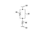
- FIG. 2 is a circuit configuration diagram of the failure prediction circuit 40 in the semiconductor sensor 10 of the present embodiment.
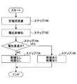
- FIG. 3 shows a flowchart of an example of a control routine executed by the controller 60 of the failure prediction circuit 40 in the semiconductor sensor 10 of the present embodiment.
- the failure prediction circuit 40 includes a parallel circuit in which a first fixed resistance portion 46 and a high potential electric conductor portion 42 are connected in parallel to each other, and the first fixed resistance portion 46 and a high-potential electric conductor portion 42 are connected in parallel to each other, and a second fixed resistor portion 48 is connected in series between the electrode portions 50 and 52 in series.
- the controller 60 supplies a constant current from the first electrode unit 50 to the second electrode unit 52 (step 100). If no condensation occurs on the surface of the Si substrate 12 and no disconnection due to electrolytic corrosion occurs in the electrical conductor portions 42 and 44 (specifically, the high potential conductor portion 42), the controller 60 can The current input to the first electrode unit 50 is the side of the parallel circuit of the first fixed resistor unit 46 and the high potential electric conductor unit 42 that is not the first fixed resistor unit 46 (that is, the high potential electric conductor unit 42). Circulate. This input current flows through the high-potential electrical lead portion 42 and then flows toward the second electrode portion 52 via the second fixed resistance portion 48 and the low-potential electrical lead portion 44.
- the minimum separation distance between the electric conductor portion 42 and the electric conductor portion 44 is any two electrode portions or electric wiring portions selected from all the electrode portions and electric wiring portions of the electric circuit 18. Is the smallest of each distance between.
- the potential applied to the first electrode unit 50 that is, the potential applied to the high-potential electrical conductor unit 42 is the potential applied to the second electrode unit 52, that is, the potential applied to the low-potential electrical conductor unit 44. Higher than the potential applied to other circuit components of the electric circuit 18. For this reason, on the Si substrate 12, condensation is likely to occur between the high potential electrical conductor portion 42 and the low potential electrical conductor portion 44 in the electrical circuit 18, and the high potential electrical conductor portion 42 is most susceptible to electrolytic corrosion due to condensation. It is a site that tends to occur.
- the current input from the controller 60 to the first electrode portion 50 is the high-potential electric current. Since the conducting wire portion 42 cannot be circulated, the first fixed resistance portion 46 is circulated. The input current flows through the first fixed resistance portion 46 and then flows toward the second electrode portion 52 via the second fixed resistance portion 48 and the low-potential electric conducting wire portion 44.
- the failure prediction circuit 40 when the disconnection due to electrolytic corrosion due to condensation does not occur in the high potential conductor portion 42, the current input to the first electrode portion 50 flows through the high potential electrical conductor portion 42. After that, it flows through the second fixed resistance portion 48 and flows toward the second electrode portion 52. For this reason, in this case, the current value of the current input to the first electrode unit 50 and the resistance value of the second fixed resistor unit 48 are between the first electrode unit 50 and the second electrode unit 52. A relatively small potential difference is generated according to. On the other hand, if a disconnection due to electrolytic corrosion due to condensation has occurred in the high-potential lead wire portion 42, the second fixed resistance is supplied after the current input to the first electrode portion 50 flows through the first fixed resistance portion 46.
- the constant current supplied between the first electrode unit 50 and the second electrode unit 52 is 1 mA
- the resistance value of the first fixed resistor unit 46 is 1 k ⁇
- the second fixed Assuming that the resistance value of the resistance portion 48 is 4 k ⁇ , the potential difference generated between the first electrode portion 50 and the second electrode portion 52 is 4 V when the high potential conducting wire portion 42 is not disconnected.
- the potential difference generated between the first electrode portion 50 and the second electrode portion 52 is 5V. It is possible to determine whether or not condensation has occurred on the surface of the Si substrate 12 by the change in potential difference as described above.
- the controller 60 generates a potential difference between the first electrode unit 50 and the second electrode unit 52 in a situation where a constant current is supplied between the first electrode unit 50 and the second electrode unit 52. Is detected (step 102). Then, the controller 60 determines whether or not the electrical conduction of the high-potential lead wire portion 42 is interrupted based on the detected potential difference between the first electrode portion 50 and the second electrode portion 52, that is, the Si substrate 12. It is determined whether or not condensation occurs on the surface.
- the controller 60 supplies the detected potential difference between the first electrode unit 50 and the second electrode unit 52 between the first electrode unit 50 and the second electrode unit 52. It is determined whether or not it is larger than the normal potential difference determined from the current value of the constant current and the resistance value of the second fixed resistance section 48 (or a value larger than the normal potential difference by a predetermined threshold value) (step) 104). Alternatively, the controller 60 determines that the detected potential difference between the first electrode unit 50 and the second electrode unit 52 is a constant current supplied between the first electrode unit 50 and the second electrode unit 52. It is determined whether or not the current value and the series resistance value of the first fixed resistance unit 46 and the second fixed resistance unit 48 have reached the vicinity of the potential difference (abnormal potential difference).
- the controller 60 makes a negative determination, that is, when the detected potential difference between the first electrode unit 50 and the second electrode unit 52 is equal to or less than the normal potential difference, or the detected first electrode.
- the potential difference between the portion 50 and the second electrode portion 52 does not reach the vicinity of the abnormal potential difference, it is determined that the electrical conduction of the high potential conductor portion 42 is not interrupted, and the surface of the Si substrate 12 is It is determined that no condensation has occurred (step 106).
- the controller 60 makes an affirmative determination, that is, when the detected potential difference between the first electrode unit 50 and the second electrode unit 52 is larger than the normal potential difference, or the detected first electrode.
- step 108 When the potential difference between the portion 50 and the second electrode portion 52 has reached the vicinity of the abnormal potential difference, it is determined that the electrical conduction of the high potential conductor portion 42 is interrupted, and the surface of the Si substrate 12 is It is determined that condensation has occurred (step 108).
- the failure prediction circuit 40 a constant current is supplied between the two electrode portions 50 and 52 to which different potentials are applied on the surface of the Si substrate 12. Based on the generated potential difference, that is, the potential difference generated between the electrical conductor portions 42 and 44, the presence or absence of disconnection occurring in the electrical conductor portion 42 can be accurately detected, and the presence or absence of condensation occurring on the surface of the Si substrate 12 can be accurately detected. Can be detected.
- the minimum separation distance between the electric conducting wire portion 42 and the electric conducting wire portion 44 is any two electrode portions or electric wiring portions selected from all the electrode portions and electric wiring portions included in the electric circuit 18.
- moisture due to condensation is likely to adhere between the high potential electric conductor portion 42 and the low potential electric conductor portion 44 on the Si substrate 12.
- electrolytic corrosion due to condensation is most likely to occur in the high-potential electrical conductor 42. For this reason, when the dew condensation occurs on the surface of the Si substrate 12, the portion of the electric circuit 18 on the Si substrate 12 that has the earliest timing of electrolytic corrosion is the high-potential electric conductor portion 42.
- the Si substrate 12 (particularly, a portion for detecting the pressure of the detection target, that is, an electrode other than the electric wire portions 42 and 44 in the electric circuit 18 or an electric wire portion) is caused by condensation. It is possible to detect the dew condensation that has occurred on the surface of the Si substrate 12 before the failure occurs.
- the electric conductor portions 42 and 44 meander in a rectangular shape so as to continue in a folded state on the surface of the Si substrate 12.
- the shape of the electric conductive wire portions 42 and 44 on the surface of the Si substrate 12 is a shape in which the condensed moisture is easily stored when the condensation occurs on the surface of the Si substrate 12. For this reason, on the Si substrate 12, moisture adhesion due to condensation is promoted between the high potential electrical conductor portion 42 and the low potential electrical conductor portion 44 in the electrical circuit 18, and electrolytic corrosion of the high potential electrical conductor portion 42 is promoted. Is promoted. Therefore, the failure prediction circuit 40 can accurately and quickly detect condensation on the surface of the Si substrate 12.
- the high-potential electrical conductor portion 42 and the low-potential electrical conductor portion 44 are each of the general materials used mainly for forming a thin film in a semiconductor process. It is formed of a metal thin film made of aluminum having the largest ionization tendency. The greater the ionization tendency, the shorter the time until disconnection due to electrical corrosion of the high-potential electrical conductor 42 when condensation occurs. Therefore, the failure prediction circuit 40 can improve sensitivity in detecting dew condensation on the surface of the Si substrate 12.
- the high potential electrical conductor portion 42 is formed on the surface of the Si substrate 12 except for the failure prediction circuit 40 in the low potential electrical conductor portion 44 and the electrical circuit 18. It is arranged near the low potential electric conductor 44 between the circuit components (electrode part, electric conductor, etc.). Generally, when moisture adheres between two electrodes having a potential difference, electrolytic corrosion occurs at the high potential side electrode.
- the failure prediction circuit 40 is subject to electrolytic corrosion caused by dew condensation in the electrode portions or the electric wire portions other than the electric wire portions 42 and 44 in the electric circuit 18. It is possible to avoid the failure of the semiconductor sensor 10.
- the semiconductor sensor 10 it is possible to detect the dew condensation occurring on the surface of the Si substrate 12 before causing the failure of the pressure sensor portion, thereby causing the dew condensation.
- the pressure of the detection target it is possible to prevent the pressure of the detection target from being normally detected until the Si substrate 12 is replaced / repaired after the failure of the pressure sensor portion.
- the Si substrate 12 is described in the “semiconductor element” described in the claims, and the high potential electric conductor portion 42 and the low potential electric conductor portion 44 are described in the claims. Whether the electrical conduction of the high-potential lead wire portion 42 is interrupted based on the potential difference between the first electrode portion 50 and the second electrode portion 52 detected by the controller 60 in the “two electric lead wire portions”.
- the first fixed resistance portion 46 is described in the claims.
- the first electrode unit 50 is described in the claims “first electrode unit”
- the second fixed resistor unit 48 is described in the claims “second resistor”. Of the second electrode portion 52 described in the claims.
- the controller 60 is arranged between the first electrode unit 50 on the high potential side and the second electrode unit 52 on the low potential side between the first electrode unit 50 and the second electrode unit 52. Supplying a constant current corresponds to “constant current distribution means” described in the claims.
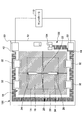
- FIG. 4 shows a top view of the semiconductor sensor 100 according to the second embodiment of the present invention.
- the same components as those of the first embodiment shown in FIG. 1 are denoted by the same reference numerals, and the description thereof is omitted or simplified.
- the semiconductor sensor 100 of the present embodiment is a sensor used for automobile engine control, exhaust purification control, barometer, and the like, similar to the semiconductor sensor 10 of the first embodiment described above.
- the semiconductor sensor 100 can be used, for example, to detect pressure in an exhaust path through which exhaust gas discharged from an internal combustion engine flows. Further, the semiconductor sensor 100 can be used to detect a pressure difference between the upstream side and the downstream side of a filter installed in the exhaust path. Furthermore, the semiconductor sensor 100 can be used as a particulate quantity detection sensor that detects the particulate quantity deposited on the filter based on the pressure difference between the upstream side and the downstream side of the filter installed in the exhaust path.
- the semiconductor sensor 100 includes a failure prediction circuit (that is, a dew condensation detection circuit) 102 for determining the presence or absence of dew condensation on the surface of the Si substrate 12 as a semiconductor element.
- the failure prediction circuit 102 has the same function as the failure prediction circuit 40 as a part of the electric circuit 18 in the first embodiment described above, and the semiconductor sensor 100 of this embodiment is replaced with the failure prediction circuit 40. This is realized by using the failure prediction circuit 102.
- the failure prediction circuit 102 is formed on the Si substrate 12 in the same process as other circuit parts of the electric circuit 18.
- the failure prediction circuit 102 has two electric conductor portions 42 and 44, one fixed resistance portion 104, and two electrode portions 50 and 52.
- the failure prediction circuit 40 according to the first embodiment is used when a constant current is supplied between the two electrode portions 50 and 52, and includes the two fixed resistance portions 46 and 48, while the failure prediction circuit according to the second embodiment. 102 is used when a constant voltage is applied between the two electrode portions 50 and 52, and includes one fixed resistance portion 104.
- One end of a high-potential electric conductor portion 42 is connected to the first electrode portion 50.
- One end of the fixed resistance portion 104 is connected to the other end of the high potential electric conducting wire portion 42.
- the fixed resistance unit 104 is provided on the same side as the side connecting the first electrode unit 50 and the second electrode unit 52 of the Si substrate 12.
- the other end of the fixed resistor portion 104 is connected to one end of the low potential electric conducting wire portion 44.
- the fixed resistance portion 104 is formed of an impurity layer made of boron or phosphorus.
- the second electrode portion 52 On the conducting wire of the low potential electric conducting wire portion 44, the second electrode portion 52 is interposed.
- the low-potential electrical conductor 44 extends from the second electrode 52 through the three sides of the Si substrate 12 to the vicinity of the first electrode 50 while facing the high-potential electrical conductor 42.
- the other end of the conducting wire portion 44 is closed in the vicinity of the first electrode portion 50.
- a portion of the low potential electric conducting wire portion 44 connecting the second electrode portion 52 and the vicinity of the first electrode portion 50 extends so as to pass through the three sides of the Si substrate 12, and the length of the portion is relatively long. .
- the failure prediction circuit 102 has a controller 110.
- the controller 110 is electrically connected to the first electrode portion 50 and is electrically connected to the second electrode portion 52.
- the controller 110 applies a constant potential difference (constant voltage) between the first electrode unit 50 and the second electrode unit 52.
- the controller 110 actually generates a potential difference between the first electrode unit 50 and the second electrode unit 52. Can be detected, and the presence or absence of condensation on the surface of the Si substrate 12 is determined based on the detected potential difference.
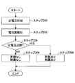
- FIG. 5 shows a flowchart of an example of a control routine executed by the controller 110 of the failure prediction circuit 102 in the semiconductor sensor 100 of the present embodiment.
- the controller 110 applies a constant voltage between the first electrode unit 50 and the second electrode unit 52 (step 200).
- the first electrode A potential difference substantially equal to the applied constant voltage is generated between the portion 50 and the second electrode portion 52.
- the voltage from the first electrode portion 50 becomes zero or the first thereof. Since the voltage signal from the electrode part 50 disappears, the potential difference generated between the first electrode part 50 and the second electrode part 52 becomes smaller than the constant voltage to be applied and does not reach the constant voltage. .
- the controller 110 In the situation where a constant voltage is applied between the first electrode unit 50 and the second electrode unit 52, the controller 110 actually generates a potential difference between the first electrode unit 50 and the second electrode unit 52. Is detected (step 202). Then, the controller 110 determines whether or not the electrical connection of the high-potential conductor portion 42 is interrupted based on the detected potential difference between the first electrode portion 50 and the second electrode portion 52, that is, the Si substrate 12. It is determined whether or not condensation occurs on the surface.
- the controller 110 detects that the detected potential difference between the first electrode unit 50 and the second electrode unit 52 is a constant voltage that is normally applied (or close to the normally applied constant voltage). It is determined whether or not a predetermined threshold value has been reached (step 204). When the controller 110 makes a negative determination, that is, when the detected potential difference between the first electrode unit 50 and the second electrode unit 52 does not reach a normal constant voltage, the high-potential lead wire It is determined that the electrical continuity of the unit 42 is not cut off, and it is determined that no condensation has occurred on the surface of the Si substrate 12 (step 206).
- the controller 60 makes an affirmative determination, that is, when the detected potential difference between the first electrode unit 50 and the second electrode unit 52 has reached a normal constant voltage, the high potential lead wire It is determined that the electrical continuity of the part 42 is cut off, and it is determined that condensation has occurred on the surface of the Si substrate 12 (step 208).
- the failure prediction circuit 102 a constant voltage is applied between the two electrode parts 50 and 52 to which different potentials are applied on the surface of the Si substrate 12. Based on the potential difference that actually occurs, that is, the potential difference that actually occurs between the electrical conductor portions 42 and 44, it is possible to accurately detect the presence or absence of disconnection that occurs in the electrical conductor portion 42, and the condensation that occurs on the surface of the Si substrate 12. Presence / absence can be accurately detected.
- the minimum separation distance between the electric conducting wire portion 42 and the electric conducting wire portion 44 is any two electrode portions or electric wiring portions selected from all the electrode portions and electric wiring portions included in the electric circuit 18.
- moisture due to condensation is likely to adhere between the high potential electric conductor portion 42 and the low potential electric conductor portion 44 on the Si substrate 12.
- electrolytic corrosion due to condensation is most likely to occur in the high-potential electrical conductor 42. For this reason, when the dew condensation occurs on the surface of the Si substrate 12, the portion of the electric circuit 18 on the Si substrate 12 that has the earliest timing of electrolytic corrosion is the high-potential electric conductor portion 42.
- the Si substrate 12 (particularly, the portion for detecting the pressure of the detection target, that is, the electrode or the electrical conductor other than the electrical conductors 42 and 44 in the electrical circuit 18) is caused by condensation. It is possible to detect the dew condensation that has occurred on the surface of the Si substrate 12 before the failure occurs.
- the electric conductor portions 42 and 44 are continuous on the surface of the Si substrate 12 while being folded in a U-shape, that is, meander in a rectangular shape.
- the shape of the electric conductive wire portions 42 and 44 on the surface of the Si substrate 12 is a shape in which the condensed moisture can be easily collected when condensation occurs on the surface of the Si substrate 12. For this reason, on the Si substrate 12, moisture adhesion due to condensation is promoted between the high potential electrical conductor portion 42 and the low potential electrical conductor portion 44 in the electrical circuit 18, and electrolytic corrosion of the high potential electrical conductor portion 42 is promoted. Is promoted. Therefore, the failure prediction circuit 102 can detect condensation on the surface of the Si substrate 12 accurately and promptly.
- the high-potential electrical conductor portion 42 and the low-potential electrical conductor portion 44 each have an ionization tendency among the general materials used mainly for thin film formation in semiconductor processes. It is formed of a metal thin film made of the largest aluminum. The greater the ionization tendency, the shorter the time until disconnection due to electrical corrosion of the high-potential electrical conductor 42 when condensation occurs. Therefore, the failure prediction circuit 102 can improve sensitivity in detecting dew condensation on the surface of the Si substrate 12.
- the high potential electrical conductor portion 42 is a circuit component other than the failure prediction circuit 40 in the low potential electrical conductor portion 44 and the electrical circuit 18 on the surface of the Si substrate 12 ( Between the electrode portion and the electric conductor portion) and the like near the low potential electric conductor portion 44. Generally, when moisture adheres between two electrodes having a potential difference, electrolytic corrosion occurs at the high potential side electrode.
- the failure prediction circuit 102 performs electrolytic corrosion caused by dew condensation on the electrode parts or the electric lead parts other than the electric lead parts 42 and 44 in the electric circuit 18. A failure of the semiconductor sensor 100 can be avoided.
- the semiconductor sensor 100 of the present embodiment it is possible to detect the dew condensation that has occurred on the surface of the Si substrate 12 before causing the failure of the pressure sensor portion, thereby causing the dew condensation.
- the pressure of the detection target it is possible to prevent the pressure of the detection target from being normally detected until the Si substrate 12 is replaced / repaired after the failure of the pressure sensor portion.
- the high potential conductor 42 is disconnected from the electrical potential based on the potential difference between the first electrode 50 and the second electrode 52 detected by the controller 110.
- the fixed resistance portion 104 is described in the claims.
- the controller 110 applies a constant voltage between the first electrode unit 50 and the second electrode unit 52 to the “resistance”, which corresponds to the “constant voltage applying unit” described in the claims. is doing.
- the shape of the electrical conductors 42 and 44 of the failure prediction circuits 40 and 102 on the surface of the Si substrate 12 is the surface of the Si substrate 12.
- the electric conductor portions 42 and 44 are respectively meandered in a rectangular shape on the surface of the Si substrate 12 in a state of being folded in a U-shape.
- the present invention is not limited to this, and the shape of the electric conductor portions 42 and 44 on the surface of the Si substrate 12 is a shape that easily collects moisture condensed on the surface of the Si substrate 12. Is sufficient, and may have the shapes shown in FIGS. 7A to 7G, or may have other shapes.
- the electric conductors 42 and 44 (1) as shown in FIG. 1, the electric conductors 42 and 44 are respectively folded in a U-shape on the surface of the Si substrate 12.
- the inner conductive wire portion 42 is linearly extended in parallel with each side on the surface of the Si substrate 12, as shown in FIG. 6.
- a shape in which a rectangular shape is continuous while extending the electric conductor 44 on the outer peripheral side in a straight line parallel to each side on the surface of the Si substrate 12, and (3) the electric conductor 42 on the inner peripheral side is made of Si.
- a rectangular shape is formed while extending linearly in parallel with each side, and the electric conductor 44 on the outer peripheral side is linearly extended in parallel with each side on the surface of the Si substrate 12.
- (4) electrical conductor 42, 4 is linearly extended parallel to each side on the surface of the Si substrate 12 and protruded in a comb-teeth shape so as to extend toward the other electric conducting wire 44, 42, (5) in FIG.
- the electric conductors 42 and 44 are respectively extended so as to be continuously folded in a triangular shape on the surface of the Si substrate 12, and (6) as shown in FIG. , 44 are respectively extended in a semi-circular folded state on the surface of the Si substrate 12, and (7) as shown in FIG.
- the inner peripheral electrical conductor portion 42 is linearly extended in parallel to each side on the surface of the Si substrate 12, and the outer peripheral electrical conductor portion 44 is linear in parallel to each side on the surface of the Si substrate 12.
- the inner conductive wire portion 42 is connected to each side on the surface of the Si substrate 12, as shown in FIG.
- the inner peripheral electrical conductor 42 is linearly extended in parallel to each side on the surface of the Si substrate 12, and the outer peripheral side
- the electric conductor 44 is extended so as to be continuous in a U-shape on the surface of the Si substrate 12, that is, to meander in a rectangular shape.
- the inner conductive wire portion 42 is linearly extended in parallel to each side on the surface of the Si substrate 12, and the outer peripheral electric wire portion 44 is continuous in a triangular shape on the surface of the Si substrate 12. The extended ones are listed.
Landscapes
- Physics & Mathematics (AREA)
- General Physics & Mathematics (AREA)
- Chemical & Material Sciences (AREA)
- Analytical Chemistry (AREA)
- Health & Medical Sciences (AREA)
- Life Sciences & Earth Sciences (AREA)
- Biochemistry (AREA)
- General Health & Medical Sciences (AREA)
- Immunology (AREA)
- Pathology (AREA)
- Investigating Or Analyzing Materials By The Use Of Electric Means (AREA)
Abstract
本発明は、半導体素子の表面に金属薄膜からなる電気回路が形成される半導体センサであって、電気回路の一部として半導体素子の表面に互いに対向して配置され、互いに異なる電位が印加される2つの電気導線部と、2つの電気導線部に生じる電位差に基づいて、半導体素子の表面に結露が発生したか否かを判別する結露検知回路と、を備える。
Description
本発明は、半導体センサに係り、特に、半導体素子の表面に金属薄膜からなる電気回路が形成されている半導体センサに関する。
従来、自動車のエンジン制御や気圧計などに用いられる半導体センサが知られている(例えば、特許文献1~4参照)。特許文献1記載の半導体センサは、半導体センサとしてダイヤフラム部を有する基板を備えており、導体とそのダイヤフラム部との電圧変化に基づいてそのダイヤフラム部の故障診断を行う。特許文献2記載の半導体センサは、半導体センサとして歪ゲージからなるブリッジ回路を備えており、ブリッジ回路と計測機器との間の配線の断線を検出する故障診断を行う。
また、特許文献3記載の半導体センサは、半導体素子のワイヤボンディングパッドにワイヤを接続し、そのワイヤからワイヤボンディングパッドに電流が流れるか否かを検出して、半導体素子の寿命による故障発生を事前に検知する故障予知を行う。特許文献4記載の半導体センサは、半導体基板上に通常の素子よりも劣化進行の早い劣化予測素子を設けると共に、その劣化予測素子の劣化度合いを検出して、劣化故障の発生を予測する故障予知を行う。
ところで、自動車のエンジン制御や気圧計などに用いられる半導体センサでは、半導体素子が筐体内に実装される。この筐体部内に湿気が浸入すると、温度変化に伴って半導体素子の表面に結露が生ずることがある。半導体素子の表面に結露が生ずると、電極部や電気導線部に電解腐食が発生して、電気的導通が絶たれる可能性がある。半導体素子で電気的導通が絶たれると、半導体素子は正常に駆動しなくなり、その結果、その半導体素子を修理・交換するまで半導体センサが正常に作動しなくなってしまう。従って、半導体素子の正常駆動を常に維持するためには、半導体素子が故障する前に、具体的には、半導体素子が結露に起因して正常に駆動する状態から駆動しない状態へ移行する前に、半導体素子の表面に発生した結露を検知することが必要である。しかしながら、従来の半導体センサ(例えば、特許文献1~4の技術)では、半導体素子表面に発生した結露を検知することができない。
本発明は、上述の点に鑑みてなされたものであり、半導体素子の結露に起因する故障発生前に半導体素子表面に発生した結露を検知することが可能な半導体センサを提供することを目的とする。
本発明の半導体センサは、半導体素子の表面に金属薄膜からなる電気回路が形成される半導体センサであって、前記電気回路の一部として半導体素子の表面上において互いに対向して配置され、互いに異なる電位が印加される2つの電気導線部と、前記2つの電気導線部に生じる電位差に基づいて、半導体素子の表面に結露が発生したか否かを判別する結露検知回路と、を備える。
上記した半導体センサにおいて、前記2つの電気導線部間の離間距離は、前記電気回路の有する任意の2つの電極部又は電気導線部の間の各距離のうち前記離間距離を除いたものの最小距離よりも小さいことが好ましい。
また、上記した半導体センサにおいて、前記2つの電気導線部のうち高電位が印加される高電位電気導線部は、半導体素子の表面上において、該2つの電気導線部のうち低電位が印加される低電位電気導線部と、前記電気回路の有する電極部又は他の電気導線部と、の間に配置されていることが好ましい。
また、上記した半導体センサにおいて、半導体素子の表面上の前記2つの電気導線部の形状は、結露した水分を溜め易い形状であることが好ましい。
また、上記した半導体センサにおいて、前記2つの電気導線部のうちの一方の電気導線部に並列に接続される第1の抵抗と、前記一方の電気導線部に接続されると共に前記第1の抵抗の一端に接続される第1の電極部と、前記一方の電気導線部及び前記第1の抵抗の他端に一端が接続する第2の抵抗と、前記2つの電気導線部のうちの他方の電気導線部に接続されると共に前記第2の抵抗の他端に接続される第2の電極部と、前記第1の電極部と前記第2の電極部との間に定電流を流通させる定電流流通手段と、を備え、前記結露検知回路は、前記定電流流通手段により前記第1の電極部と前記第2の電極部との間に定電流が流通される状況において前記第1の電極部と前記第2の電極部との電位差が通常の電位差よりも大きい場合に、半導体素子の表面に結露が生じたと判別することが好ましい。
また、上記した半導体センサにおいて、前記2つの電気導線部のうちの一方の電気導線部に接続される第1の電極部と、前記一方の電気導線部に一端が接続する抵抗と、前記2つの電気導線部のうちの他方の電気導線部に接続されると共に前記抵抗の他端に接続される第2の電極部と、前記第1の電極部と前記第2の電極部との間に定電圧を印加する定電圧印加手段と、を備え、前記結露検知回路は、前記定電圧印加手段により前記第1の電極部と前記第2の電極部との間に定電圧が印加される状況において前記2つの電気導線部に生じる電位差が前記定電圧の近傍に達していない場合に、半導体素子の表面に結露が生じたと判別することが好ましい。
また、上記した半導体センサにおいて、前記2つの電気導線部はそれぞれ、主にアルミニウムにより構成されていることが好ましい。
更に、上記した半導体センサにおいて、前記2つの電気導線部は、半導体素子の表面に形成されるダイヤフラムの外周側に配置されていることが好ましい。
本発明によれば、半導体素子の結露に起因する故障発生前に半導体素子表面に発生した結露を検知することができる。
本発明の実施の形態の半導体センサは、半導体素子の表面に金属薄膜からなる電気回路が形成される半導体センサであって、前記電気回路の一部として半導体素子の表面上において互いに対向して配置され、互いに異なる電位が印加される2つの電気導線部と、前記2つの電気導線部に生じる電位差に基づいて、半導体素子の表面に結露が発生したか否かを判別する結露検知回路と、を備える半導体センサである。
本実施の形態において、半導体素子の表面に形成される金属薄膜からなる電気回路は、その一部として、半導体素子の表面上において互いに対向して配置され、互いに異なる電位が印加される2つの電気導線部を有する。かかる構造においては、2つの電気導線部の間に温度変化に伴って生じた結露が進行すると、対向する2つの電気導線部の金属薄膜(例えば、アルミニウム)が高電位側から溶解し、電解腐食が発生して、高電位側の金属薄膜が切断されることにより、電気的導通が絶たれる。上記の構造において、電気導線部の電気的導通が保たれている場合は、2つの電気導線部間の電位差はほぼ一定であるが、電気導線部の電気的導通が絶たれると、その電気的導通が絶たれた瞬間で2つの電気導線部間の電位差に変化が生じ(電位差が上昇し)、その2つの電気導線部間の電位差が、電気的導通が保たれている場合と比べて異なるものとなる。そこで、本実施の形態において、半導体素子の表面に結露が発生したか否かは、それら2つの電気導線部に生じる電位差の変化に基づいて判別される。従って、本実施の形態によれば、半導体素子の結露に起因する故障発生前に半導体素子表面に発生した結露を検知することができる。
上記した半導体センサにおいて、前記2つの電気導線部間の離間距離は、前記電気回路の有する任意の2つの電極部又は電気導線部の間の各距離のうち前記離間距離を除いたものの最小距離よりも小さいことが好ましい。
この態様においては、半導体素子の表面に互いに対向して配置されかつ互いに異なる電位が印加される2つの電気導線部間の離間距離が、電気回路の有する任意の2つの電極部又は電気導線部の間の各距離のうちその離間距離を除いたものの最小距離よりも小さい。このため、半導体素子の表面に結露が生ずるときは、その結露に伴う水分が付着し易い部位すなわち結露による電解腐食が生じるタイミングが最も早い部位は、半導体素子上の電極部及び電気導線部のすべての組み合わせのうち、半導体素子の表面に互いに対向して配置されかつ互いに異なる電位が印加される2つの電気導線部であると考えられる。従って、半導体素子の表面に互いに対向して配置されかつ互いに異なる電位が印加される2つの電気導線部を有することにより、その2つの電気導線部に半導体素子上で最も早いタイミングで結露による電解腐食が生じるため、半導体素子の結露に起因する故障発生前に半導体素子表面に発生した結露を検知することができる。
また、上記した半導体センサにおいて、前記2つの電気導線部のうち高電位が印加される高電位電気導線部は、半導体素子の表面上において、該2つの電気導線部のうち低電位が印加される低電位電気導線部と、前記電気回路の有する電極部又は他の電気導線部と、の間に配置されていることが好ましい。
この態様においては、半導体素子の表面に互いに対向して配置されかつ互いに異なる電位が印加される2つの電気導線部のうち高電位電気導線部が、低電位電気導線部と電気回路の電極部又は他の電気導線部との間に配置される。一般的に、半導体素子の結露に起因する電解腐食は、高電位側で生じる。このため、低電位電気導線部の電位が高電位電気導線部以外の電極部又は電気導線部の電位よりも低い場合においても、高電位電気導線部と低電位電気導線部との間に結露した水分が付着する前に、その低電位電気導線部と高電位電気導線部以外の電極部又は電気導線部との間に結露した水分が溜まり難い。従って、半導体素子表面に発生した結露を検知する前に、電気回路の、半導体素子の表面に互いに対向して配置されかつ互いに異なる電位が印加される2つの電気導線部以外の電極部又は電気導線部で結露に起因する電解腐食が生ずるのを回避することができる。
また、上記した半導体センサにおいて、半導体素子の表面上の前記2つの電気導線部の形状は、結露した水分を溜め易い形状であることが好ましい。
この態様においては、半導体素子の表面に互いに対向して配置されかつ互いに異なる電位が印加される2つの電気導線部の形状が、結露した水分を溜め易い形状である。このため、半導体素子の結露に起因する故障発生前に半導体素子表面に発生した結露を検知することができ易くなる。
また、上記した半導体センサにおいて、前記2つの電気導線部のうちの一方の電気導線部に並列に接続される第1の抵抗と、前記一方の電気導線部に接続されると共に前記第1の抵抗の一端に接続される第1の電極部と、前記一方の電気導線部及び前記第1の抵抗の他端に一端が接続する第2の抵抗と、前記2つの電気導線部のうちの他方の電気導線部に接続されると共に前記第2の抵抗の他端に接続される第2の電極部と、前記第1の電極部と前記第2の電極部との間に定電流を流通させる定電流流通手段と、を備え、前記結露検知回路は、前記定電流流通手段により前記第1の電極部と前記第2の電極部との間に定電流が流通される状況において前記第1の電極部と前記第2の電極部との電位差が通常の電位差よりも大きい場合に、半導体素子の表面に結露が生じたと判別することが好ましい。
この態様においては、第1の電極部と第2の電極部との間に定電流が流通すると、一方の電気導線部の電気的導通が保たれている場合は、流通電流は主にその一方の電気導線部側を流れるので、第1の電極部と第2の電極部との電位差は比較的小さくなる。一方、一方の電気導線部の電気的導通が絶たれている場合は、流通電流は主に第1の抵抗側を流れるので、第1の電極部と第2の電極部との電位差は比較的大きくなる。従って、第1の電極部と第2の電極部との電位差が比較的大きい場合に、半導体素子の表面に結露が生じたと判別することとすれば、その結露の有無を精度よく検知することができ易くなる。
また、上記した半導体センサにおいて、前記2つの電気導線部のうちの一方の電気導線部に接続される第1の電極部と、前記一方の電気導線部に一端が接続する抵抗と、前記2つの電気導線部のうちの他方の電気導線部に接続されると共に前記抵抗の他端に接続される第2の電極部と、前記第1の電極部と前記第2の電極部との間に定電圧を印加する定電圧印加手段と、を備え、前記結露検知回路は、前記定電圧印加手段により前記第1の電極部と前記第2の電極部との間に定電圧が印加される状況において前記2つの電気導線部に生じる電位差が前記定電圧の近傍に達していない場合に、半導体素子の表面に結露が生じたと判別することが好ましい。
この態様においては、第1の電極部と第2の電極部との間に定電圧が印加されると、一方の電気導線部の電気的導通が保たれている場合は、2つの電気導線部の電位差はほぼ上記の定電圧となる。一方、一方の電気導線部の電気的導通が絶たれている場合は、2つの電気導線部の電位差は上記の定電圧に達しない。従って、2つの電気導線部の電位差が上記の定電圧よりも小さい場合に、半導体素子の表面に結露が生じたと判別することとすれば、その結露の有無を精度よく検知することができ易くなる。
また、上記した半導体センサにおいて、前記2つの電気導線部はそれぞれ、主にアルミニウムにより構成されていることが好ましい。
更に、上記した半導体センサにおいて、前記2つの電気導線部は、半導体素子の表面に形成されるダイヤフラムの外周側に配置されていることが好ましい。
以下、図面を用いて、本発明に係る半導体センサの具体的な実施の形態について説明する。
図1は、本発明の第1実施形態に係る半導体センサ10の上面図を示す。
本実施形態の半導体センサ10は、自動車のエンジン制御、排気浄化制御、又は気圧計などに用いられる圧力センサである。半導体センサ10は、例えば、内燃機関から排出される排気ガスが流通する排気経路内の圧力を検出するために用いることができる。また、半導体センサ10は、排気経路に設置されるフィルタの上流側と下流側との圧力差を検出するために用いることができる。更には、半導体センサ10は、排気経路に設置されるフィルタの上流側と下流側との圧力差に基づいてそのフィルタに堆積するパティキュレート量を検出するパティキュレート量検出センサに用いることができる。
図1に示す如く、半導体センサ10は、半導体素子としてのシリコン(Si)基板12を備えている。半導体センサ10は、Si基板12に対する周知の半導体製造技術を施すことにより製造される。Si基板12は、四つの辺により区画された平面略矩形の板状部材である。Si基板12には、主裏面に凹状に空いた開口部14(図1において破線で囲まれた部分)が形成されている。開口部14は、Si基板12を異方性エッチングすることにより形成される。開口部14は、4つのダイヤフラム側壁により囲まれる空間を構成している。
開口部14の主表面側には、薄肉(薄板)のダイヤフラム16が形成されている。開口部14及びダイヤフラム16は、Si基板12の表面のほぼ中央に配置されている。ダイヤフラム16は、表裏の圧力差に応じた量だけ撓むことが可能な薄い部材である。ダイヤフラム16の平面形状は、二組の互いに平行に向かい合う一対の辺により囲まれる略正方形である矩形形状である。ダイヤフラム16は、Si基板12を異方性エッチングすることにより開口部14が形成されることに伴って形成される。
Si基板12には、電気回路18が形成されている。電気回路18は、ボロン又はリン等から成る不純物層やアルミニウム等から成る金属薄膜層により構成される。電気回路18の不純物層は、Si基板12内部に形成される。また、電気回路18の金属薄膜層は、Si基板12の表面に形成される。
ダイヤフラム16上には、そのダイヤフラム16の撓みに応じた検出信号を出力する歪ゲージ20,22,24,26が配置されている。歪ゲージ20,22,24,26は、Si基板12の主表面に不純物のイオン注入や拡散を施すことにより形成される。各歪ゲージ20,22,24,26はそれぞれ、ダイヤフラム16の配置部位における撓みに伴う基準からの抵抗値変化に応じた検出信号を出力するピエゾ抵抗である。
歪ゲージ20,22は、ダイヤフラム16の表面全体の部位の中でダイヤフラム16への被検出対象の圧力印加時にダイヤフラム16が最も圧縮される部位である中心近傍(重心付近)に配置されるセンターゲージである。また、歪ゲージ24,26は、ダイヤフラム16の表面全体の部位の中でダイヤフラム16への被検出対象の圧力印加時にダイヤフラム16が最も引っ張られる部位である開口部14のダイヤフラム側壁に近い周辺部(特に、ダイヤフラム16を構成する辺の中点近傍)に配置されるサイドゲージである。以下、適宜、歪ゲージ20,22をセンターゲージ20,22と、また、歪ゲージ24,26をサイドゲージ24,26と、それぞれ称す。センターゲージ20,22とサイドゲージ24,26とは、応力に対する抵抗値の変化の方向が逆となるように設けられている。
歪ゲージ20,22,24,26は、Si基板12の主表面に不純物のイオン注入や拡散を施すことにより形成される拡散リード28を介して結線され、電気的に接続されている。歪ゲージ20,22,24,26は、拡散リード28により互いに直列接続された閉回路であるホイートストンブリッジ回路を構成している。拡散リード28は、Si基板12の全体の中で四隅に分かれるように4分割された広範な領域を有している。各拡散リード28の領域は、ダイヤフラム16の表面全体の部位の中で四隅を含んでおり、絶縁層であるシリコン酸化膜を介して画成されている。
Si基板12の主表面には、拡散リード28に接続されるコンタクトホール30及び電極32が形成されている。コンタクトホール30及び電極32はそれぞれ、4つずつ設けられている。コンタクトホール30及び電極32は、歪ゲージ20,22,24,26と外部の検出装置とを電気的に接続して、上記のホイートストンブリッジ回路へ電圧を印加し或いはホイートストンブリッジ回路からの検出信号を出力するために設けられている。コンタクトホール30及び電極32は、Si基板12の主表面上の層間絶縁膜であるシリコン酸化膜上に、アルミニウムを用いた蒸着等により金属薄膜で形成される。
上記のホイートストンブリッジ回路において、2つの入力電極32の間に直流定電圧Vが与えられていると、ダイヤフラム16の撓みが歪ゲージ20,22,24,26の抵抗値の変化として現われ、2つの出力電極32の間に被検出対象の圧力に応じたレベルの電圧検出信号が出力されることとなる。
上記した構造を有する半導体センサ10は、Si基板12の主裏面にガラス台座等が陽極接合等により接合されている。Si基板12の主裏面側に形成される開口部14内は、ガラス台座等への接合が行われていると、真空等の一定の圧力に保たれて封止されることで、以後、圧力基準室として扱うことができる。また、半導体センサ10は、筐体内に実装される。
このような半導体センサ10の構造においては、Si基板12の主表面側に被検出対象の圧力が印加されると、印加圧力に応じてダイヤフラム16の撓みが発生する。この際には、ダイヤフラム16の撓みにより各歪ゲージ20,22,24,26の抵抗値が変化して、各歪ゲージ20,22,24,26から印加圧力に応じた電圧検出信号が出力される。かかる電圧信号は、電極32から外部の検出装置へ送られて信号処理される。これにより、外部の検出装置において被検出対象の圧力が検出される。
また、本実施形態の半導体センサ10は、半導体素子としてのSi基板12の表面における結露の有無を判定するための故障予知回路(すなわち、結露検知回路)40を備えている。故障予知回路40は、結露による電解腐食に起因してSi基板12が故障する前にその故障を予知する回路であって、圧力検出のための回路と共に、Si基板12に形成される電気回路18の一部を構成している。かかる故障予知回路40によれば、Si基板12の表面に発生した結露を、圧力センサ部分の故障を生じさせる前に検知することが可能であり、これにより、結露に起因して圧力センサ部分の故障が生じてからSi基板12の交換・修理が行われるまでの間、被検出対象の圧力を正常に検知することができなくなるのを防止することが可能である。
故障予知回路40は、電気回路18の他の回路部位と同様のプロセスでSi基板12に形成される。故障予知回路40は、2つの電気導線部42,44と、2つの固定抵抗部46,48と、2つの電極部50,52と、を有している。
電気導線部42,44はそれぞれ、Si基板12の表面上において、ほぼ中央に配置されたダイヤフラム16の外周側に設けられている。電気導線部42,44はそれぞれ、Si基板12の表面上においてダイヤフラム16の周囲を取り囲むように延在している。2つの電気導線部42,44は、Si基板12の表面上においてダイヤフラム16のほぼ全周にわたって互いに対向して配置されている。
電気導線部42,44はそれぞれ、Si基板12の表面上においてコの字状に折り畳まれた状態で連続するようにすなわち矩形状に蛇行するように延びている。電気導線部42,44の、Si基板12の表面上での形状は、Si基板12表面に結露が生ずる際に結露した水分を溜め易い形状である。電気導線部42と電気導線部44との間の最小となる離間距離(すなわち両導線部42,44間の対向距離)は、電気回路18の有するすべての電極部及び電気配線部から選んだ任意の2つの電極部又は電気配線部の間の各距離のうち、その電気導線部42と電気導線部44との間の最小となる離間距離を除いたものの最小距離よりも小さい。すなわち、電気導線部42と電気導線部44との間の最小となる離間距離は、電気回路18の有するすべての電極部及び電気配線部から選んだ任意の2つの電極部又は電気配線部の間の各距離のうちで最小である。
電気導線部42,44は、Si基板12の表面上において電気回路18の、故障予知回路40以外の回路部品(例えば電極32など)の外周側に配置されている。Si基板12の表面上において、電気導線部42は内周側(ダイヤフラム16側)に配置されており、かつ、電気導線部44は外周側(Si基板12の外縁側)に配置されている。電気導線部42,44はそれぞれ、主に、半導体プロセスの薄膜形成で用いられる一般的な材料の中でイオン化傾向の最も大きいアルミニウムからなる金属薄膜で形成されている。
内周側の電気導線部42には、第1の電極部50が接続されている。また、外周側の電気導線部44には、第2の電極部52が接続されている。電極部50,52はそれぞれ、主にアルミニウムからなる金属薄膜で形成されている。第1の電極部50には、高電位が印加されている。また、第2の電極部52には、低電位が印加されている。このため、電気導線部42には第1の電極部50を介して高電位が印加されており、また、電気導線部44には第2の電極部52を介して低電位が印加されている。
第1の電極部50に印加される電位は、第2の電極部52に印加される電位よりも高く、更には、電気回路18の他の回路部品に印加される電位よりも高い値に設定されている。以下、適宜、電気導線部42を高電位電気導線部42と、電気導線部44を低電位電気導線部44と、それぞれ称す。高電位電気導線部42は、Si基板12の表面上において、低電位電気導線部44と電気回路18の故障予知回路40以外の回路部品との間に低電位電気導線部44寄りに配置されている。
電極部50,52はそれぞれ、Si基板12の表面上においてSi基板12の角部に配置されている。第1の電極部50には、高電位電気導線部42の一端が接続されている。高電位電気導線部42は、第1の電極部50からSi基板12の各辺を経由してその第1の電極部50近傍まで低電位電気導線部44に対向しつつ延びている。高電位電気導線部42は、Si基板12の表面上において蛇行しながらSi基板12の各辺に対して平行になるように延びている。第1の電極部50には、また、予め抵抗値が所定値に固定された第1の固定抵抗部46の一端が接続されている。第1の固定抵抗部46は、第1の電極部50の近傍に設けられている。第1の固定抵抗部46の他端は、高電位電気導線部42の他端に接続されている。第1の固定抵抗部46は、高電位電気導線部42に並列に接続されている。
高電位電気導線部42の一端と他端との間には、予め抵抗値が所定値に固定された第2の固定抵抗部48の一端が接続されている。第2の固定抵抗部48の一端は、高電位電気導線部42と共に、第1の固定抵抗部46の他端に接続されている。第2の固定抵抗部48は、Si基板12の第1の固定抵抗部46が設けられた辺と同じ辺上に設けられている。第2の固定抵抗部48の他端は、低電位電気導線部44の一端に接続されている。固定抵抗部46,48はそれぞれ、ボロン又はリン等から成る不純物層で形成されている。
低電位電気導線部44の導線上には、第2の電極部52が介在している。第2の電極部52は、低電位電気導線部44を介して第2の固定抵抗部48の他端に接続されている。第2の電極部52と第2の固定抵抗部48とは、互いに近接して配置されており、同じSi基板12の辺上に設けられている。低電位電気導線部44の、第2の電極部52と第2の固定抵抗部48とを結ぶ部位はSi基板12の一辺上に延びており、その部位の長さは比較的短い。
また、低電位電気導線部44は、第2の電極部52からSi基板12の三辺を経由して第1の電極部50近傍まで高電位電気導線部42に対向しつつ延びており、低電位電気導線部44の他端は、第1の電極部50近傍で閉じられている。低電位電気導線部44の、第2の電極部52と第1の電極部50近傍とを結ぶ部位はSi基板12の三辺を通るように延びており、その部位の長さは比較的長い。
故障予知回路40は、コントローラ60を有している。コントローラ60には、第1の電極部50が電気的に接続されていると共に、第2の電極部52が電気的に接続されている。コントローラ60は、第1の電極部50と第2の電極部52との間に高電位側の第1の電極部50から低電位側の第2の電極部52へ向けて一定の電流(定電流)を供給する。コントローラ60は、第1の電極部50と第2の電極部52との間に定電流を供給している状況においてその第1の電極部50と第2の電極部52との間に生ずる電位差を検知することが可能であり、その検知電位差に基づいてSi基板12の表面における結露の有無を判定する。
以下、図2及び図3を参照して、故障予知回路40による故障検知の手法について説明する。
図2は、本実施形態の半導体センサ10における故障予知回路40の回路構成図を示す。また、図3は、本実施形態の半導体センサ10において故障予知回路40のコントローラ60が実行する制御ルーチンの一例のフローチャートを示す。
図2に示す如く、故障予知回路40は、第1の固定抵抗部46と高電位電気導線部42とが互いに並列に接続された並列回路を有していると共に、その第1の固定抵抗部46と高電位電気導線部42とが互いに並列に接続された並列回路と第2の固定抵抗部48とが電極部50,52間で直列に接続された直列回路と、を有している。
コントローラ60は、第1の電極部50から第2の電極部52へ向けて定電流を供給する(ステップ100)。Si基板12の表面に結露が生じておらず、電気導線部42,44(具体的には、高電位導線部42)に電解腐食に起因する断線が生じていない場合には、コントローラ60から第1の電極部50に入力した電流は、第1の固定抵抗部46と高電位電気導線部42との並列回路の中で第1の固定抵抗部46でない側(すなわち高電位電気導線部42)を流通する。この入力電流は、高電位電気導線部42を流通した後、第2の固定抵抗部48及び低電位電気導線部44を介して第2の電極部52へ向けて流れる。
一方、Si基板12の表面に結露が生じると、最終的に、電気回路18の各種の電極部や電気導線部に電解腐食が発生することで、電気的導通が絶たれる。一般に、電位差が生じている2つの電極間に水分が付着した場合、電解腐食は、高電位側の電極で発生する。また、2つの電極間の距離が短いほど、より少ない量の水分で両電極が接するので、電解腐食が生じ易い。
上記の如く、電気導線部42と電気導線部44との間の最小となる離間距離は、電気回路18の有するすべての電極部及び電気配線部から選んだ任意の2つの電極部又は電気配線部の間の各距離のうちで最小である。また、第1の電極部50に印加される電位すなわち高電位電気導線部42に印加される電位は、第2の電極部52に印加される電位すなわち低電位電気導線部44に印加される電位よりも高く、更には、電気回路18の他の回路部品に印加される電位よりも高い値に設定されている。このため、Si基板12上では、電気回路18の中で高電位電気導線部42と低電位電気導線部44との間で結露が生じ易く、高電位電気導線部42が最も結露による電解腐食が生じ易い部位である。
Si基板12の表面に結露が生じ、高電位電気導線部42に結露による電解腐食が生じて断線が生じた場合には、コントローラ60から第1の電極部50に入力した電流は、高電位電気導線部42を流通することができないので、第1の固定抵抗部46を流通する。この入力電流は、第1の固定抵抗部46を流通した後、第2の固定抵抗部48及び低電位電気導線部44を介して第2の電極部52へ向けて流れる。
このように、故障予知回路40において、高電位導線部42に結露による電解腐食に起因する断線が生じていない場合は、第1の電極部50に入力した電流が高電位電気導線部42を流通した後に第2の固定抵抗部48を流通し第2の電極部52へ向けて流れる。このため、この場合は、第1の電極部50と第2の電極部52との間に、第1の電極部50に入力した電流の電流値と第2の固定抵抗部48の抵抗値とに応じた比較的小さな電位差が生じる。一方、高電位導線部42に結露による電解腐食に起因する断線が生じていた場合は、第1の電極部50に入力した電流が第1の固定抵抗部46を流通した後に第2の固定抵抗部48を流通し第2の電極部52へ向けて流れる。このため、この場合は、第1の電極部50と第2の電極部52との間に、第1の電極部50に入力した電流の電流値と第1の固定抵抗部46と第2の固定抵抗部48との直列抵抗値とに応じた比較的大きな電位差が生じる。
例えば、第1の電極部50と第2の電極部52との間に供給される定電流が1mAであり、第1の固定抵抗部46の抵抗値が1kΩであり、かつ、第2の固定抵抗部48の抵抗値が4kΩであるとすると、高電位導線部42に断線が生じていない場合は、第1の電極部50と第2の電極部52との間に生じる電位差が4Vとなる。一方、高電位導線部42に断線が生じている場合は、第1の電極部50と第2の電極部52との間に生じる電位差が5Vとなる。上記のような電位差の変化により、Si基板12の表面に結露が生じているか否かを判断することが可能となる。
コントローラ60は、第1の電極部50と第2の電極部52との間に定電流を供給している状況においてその第1の電極部50と第2の電極部52との間に生ずる電位差を検知する(ステップ102)。そして、コントローラ60は、検知した第1の電極部50と第2の電極部52との間の電位差に基づいて高電位導線部42の電気的導通が絶たれているか否かすなわちSi基板12の表面に結露が生じているか否かを判別する。
具体的には、コントローラ60は、検知した第1の電極部50と第2の電極部52との間の電位差が、第1の電極部50と第2の電極部52との間に供給される定電流の電流値と第2の固定抵抗部48の抵抗値とから定まる通常の電位差(或いは、その通常の電位差よりも所定の閾値だけ大きい値)よりも大きいか否かを判別する(ステップ104)。或いは、コントローラ60は、検知した第1の電極部50と第2の電極部52との間の電位差が、第1の電極部50と第2の電極部52との間に供給される定電流の電流値と第1の固定抵抗部46と第2の固定抵抗部48との直列抵抗値とから定まる電位差(異常の電位差)の近傍に達しているか否かを判別する。
そして、コントローラ60は、否定判定を行った場合、すなわち、検知した第1の電極部50と第2の電極部52との間の電位差が通常の電位差以下である場合又は検知した第1の電極部50と第2の電極部52との間の電位差が異常の電位差近傍に達していない場合は、高電位導線部42の電気的導通が絶たれていないと判定し、Si基板12の表面に結露が生じていないと判定する(ステップ106)。一方、コントローラ60は、肯定判定を行った場合、すなわち、検知した第1の電極部50と第2の電極部52との間の電位差が通常の電位差よりも大きい場合又は検知した第1の電極部50と第2の電極部52との間の電位差が異常の電位差近傍に達している場合は、高電位導線部42の電気的導通が絶たれていると判定し、Si基板12の表面に結露が生じていると判定する(ステップ108)。
従って、故障予知回路40においては、Si基板12の表面上において互いに異なる電位が印加される2つの電極部50,52間に定電流が供給される状況でその2つの電極部50,52間に生じる電位差すなわち電気導線部42,44間に生じる電位差に基づいて、電気導線部42に発生する断線の有無を精度よく検知することができ、Si基板12の表面に発生する結露の有無を精度よく検知することができる。
上述の如く、電気導線部42と電気導線部44との間の最小となる離間距離は、電気回路18の有するすべての電極部及び電気配線部から選んだ任意の2つの電極部又は電気配線部の間の各距離のうちで最小であるので、Si基板12上では、電気回路18の中で高電位電気導線部42と低電位電気導線部44との間に結露に伴う水分が付着し易く、高電位電気導線部42に最も結露による電解腐食が生じ易い。このため、Si基板12の表面上に結露が生じた際にSi基板12上の電気回路18の中で電解腐食するタイミングが最も早い部位は、高電位電気導線部42である。従って、故障予知回路40においては、Si基板12(特に、被検出対象の圧力を検知する部位すなわち電気回路18内の電気導線部42,44以外の電極又は電気導線部など)に結露に起因した故障が生じる前にSi基板12の表面に発生した結露を検知することができる。
また、本実施形態の故障予知回路40において、上記の如く、電気導線部42,44は、Si基板12の表面上においてコの字状に折り畳まれた状態で連続するようにすなわち矩形状に蛇行するように延びており、電気導線部42,44の、Si基板12の表面上での形状は、Si基板12表面に結露が生ずる際にその結露した水分を溜め易い形状である。このため、Si基板12上では、電気回路18の中で高電位電気導線部42と低電位電気導線部44との間に結露に伴う水分付着が促進され、高電位電気導線部42の電解腐食が促進される。従って、故障予知回路40は、Si基板12の表面への結露検知を精度よくかつ速やかに行うことができる。
また、本実施形態の故障予知回路40において、上記の如く、高電位電気導線部42及び低電位電気導線部44はそれぞれ、主に、半導体プロセスの薄膜形成で用いられる一般的な材料の中でイオン化傾向の最も大きいアルミニウムからなる金属薄膜で形成されている。イオン化傾向が大きいほど、結露発生時に高電位電気導線部42の電気腐食による断線までの時間が短くなる。従って、故障予知回路40は、Si基板12の表面の結露検知を行ううえで感度を向上させることが可能である。
また、本実施形態の故障予知回路40において、上記の如く、高電位電気導線部42は、Si基板12の表面上において、低電位電気導線部44と電気回路18での故障予知回路40以外の回路部品(電極部及び電気導線部など)との間に低電位電気導線部44寄りに配置されている。一般に、電位差が生じている2つの電極間に水分が付着した場合、電解腐食は、高電位側の電極で発生する。このため、低電位電気導線部44の電位が電気回路18内の高電位電気導線部42以外の電極部又は電気導線部の電位よりも低い場合においても、その低電位電気導線部44と高電位電気導線部42との間に結露した水分が付着する前に、その低電位電気導線部44とその電気回路18内の高電位電気導線部42以外の電極部又は電気導線部との間に結露した水分が溜まり難い。従って、故障予知回路40は、Si基板12の表面に発生した結露を検知する前に、電気回路18内の電気導線部42,44以外の電極部又は電気導線部で結露に起因する電解腐食すなわち半導体センサ10の故障が生ずるのを回避することができる。
このように、本実施形態の半導体センサ10においては、Si基板12の表面に発生した結露を、圧力センサ部分の故障を生じさせる前に検知することが可能であり、これにより、結露に起因して圧力センサ部分の故障が生じてからSi基板12の交換・修理が行われるまでの間、被検出対象の圧力を正常に検知することができなくなるのを防止することが可能である。
尚、上記の第1実施形態においては、Si基板12が特許請求の範囲に記載した「半導体素子」に、高電位電気導線部42及び低電位電気導線部44が特許請求の範囲に記載した「2つの電気導線部」に、コントローラ60が検知した第1の電極部50と第2の電極部52との間の電位差に基づいて高電位導線部42の電気的導通が絶たれているか否かを判別してSi基板12の表面に結露が生じているか否かを判別することが特許請求の範囲に記載した「結露検知回路」に、第1の固定抵抗部46が特許請求の範囲に記載した「第1の抵抗」に、第1の電極部50が特許請求の範囲に記載した「第1の電極部」に、第2の固定抵抗部48が特許請求の範囲に記載した「第2の抵抗」に、第2の電極部52が特許請求の範囲に記載した「第2の電極部」に、コントローラ60が第1の電極部50と第2の電極部52との間に高電位側の第1の電極部50から低電位側の第2の電極部52へ向けて定電流を供給することが特許請求の範囲に記載した「定電流流通手段」に、それぞれ相当している。
図4は、本発明の第2実施形態に係る半導体センサ100の上面図を示す。尚、図4において、上記図1に示す第1実施形態の構成と同一の構成部分については、同一の符号を付してその説明を省略又は簡略する。
本実施形態の半導体センサ100は、上記した第1実施形態の半導体センサ10と同様に、自動車のエンジン制御や排気浄化制御,気圧計などに用いられるセンサである。半導体センサ100は、例えば、内燃機関から排出される排気ガスが流通する排気経路内の圧力を検出するために用いることができる。また、半導体センサ100は、排気経路に設置されるフィルタの上流側と下流側との圧力差を検出するために用いることができる。更には、半導体センサ100は、排気経路に設置されるフィルタの上流側と下流側との圧力差に基づいてそのフィルタに堆積するパティキュレート量を検出するパティキュレート量検出センサに用いることができる。
図4に示す如く、半導体センサ100は、半導体素子としてのSi基板12の表面における結露の有無を判定するための故障予知回路(すなわち、結露検知回路)102を備えている。故障予知回路102は、上記した第1実施形態における電気回路18の一部としての故障予知回路40と同様の機能を有しており、本実施形態の半導体センサ100は、故障予知回路40に代えて故障予知回路102を用いることにより実現される。故障予知回路102は、電気回路18の他の回路部位と同様のプロセスでSi基板12に形成される。故障予知回路102は、2つの電気導線部42,44と、1つの固定抵抗部104と、2つの電極部50,52と、を有している。第1実施形態の故障予知回路40は、2つの電極部50,52間に定電流を供給する場合に用いられ、2つの固定抵抗部46,48を備える一方、第2実施形態の故障予知回路102は、2つの電極部50,52間に定電圧を印加する場合に用いられ、一つの固定抵抗部104を備える。
第1の電極部50には、高電位電気導線部42の一端が接続されている。高電位電気導線部42の他端には、固定抵抗部104の一端が接続されている。固定抵抗部104は、Si基板12の第1の電極部50と第2の電極部52とを結ぶ辺と同じ辺上に設けられている。固定抵抗部104の他端は、低電位電気導線部44の一端に接続されている。固定抵抗部104は、ボロン又はリン等から成る不純物層で形成されている。
低電位電気導線部44の導線上には、第2の電極部52が介在している。低電位電気導線部44は、第2の電極部52からSi基板12の三辺を経由して第1の電極部50近傍まで高電位電気導線部42に対向しつつ延びており、低電位電気導線部44の他端は、第1の電極部50近傍で閉じられている。低電位電気導線部44の、第2の電極部52と第1の電極部50近傍とを結ぶ部位はSi基板12の三辺を通るように延びており、その部位の長さは比較的長い。
故障予知回路102は、コントローラ110を有している。コントローラ110には、第1の電極部50が電気的に接続されていると共に、第2の電極部52が電気的に接続されている。コントローラ110は、第1の電極部50と第2の電極部52との間に一定の電位差(定電圧)を印加する。コントローラ110は、第1の電極部50と第2の電極部52との間に定電圧を印加する状況においてその第1の電極部50と第2の電極部52との間に実際に生ずる電位差を検知することが可能であり、その検知電位差に基づいてSi基板12の表面における結露の有無を判定する。
以下、図5を参照して、故障予知回路102による故障検知の手法について説明する。
図5は、本実施形態の半導体センサ100において故障予知回路102のコントローラ110が実行する制御ルーチンの一例のフローチャートを示す。
コントローラ110は、第1の電極部50と第2の電極部52との間に定電圧を印加する(ステップ200)。Si基板12の表面に結露が生じておらず、電気導線部42,44(具体的には、高電位導線部42)に電解腐食に起因する断線が生じていない場合には、第1の電極部50と第2の電極部52との間に、印加される定電圧とほぼ同じ電位差が生じる。一方、Si基板12の表面に結露が生じ、高電位電気導線部42に結露による電解腐食が生じて断線が生じた場合には、第1の電極部50からの電圧がゼロとなり或いはその第1の電極部50からの電圧信号が消滅するため、第1の電極部50と第2の電極部52との間に生じる電位差が、印加されるべき定電圧よりも小さくなりその定電圧に達しなくなる。
コントローラ110は、第1の電極部50と第2の電極部52との間に定電圧を印加する状況においてその第1の電極部50と第2の電極部52との間に実際に生ずる電位差を検知する(ステップ202)。そして、コントローラ110は、検知した第1の電極部50と第2の電極部52との間の電位差に基づいて高電位導線部42の電気的導通が絶たれているか否かすなわちSi基板12の表面に結露が生じているか否かを判別する。
具体的には、コントローラ110は、検知した第1の電極部50と第2の電極部52との間の電位差が、通常印加される定電圧(或いは、その通常印加される定電圧の近傍に定められた閾値)に達しているか否かを判別する(ステップ204)。そして、コントローラ110は、否定判定を行った場合、すなわち、検知した第1の電極部50と第2の電極部52との間の電位差が通常の定電圧に達していない場合は、高電位導線部42の電気的導通が絶たれていないと判定し、Si基板12の表面に結露が生じていないと判定する(ステップ206)。一方、コントローラ60は、肯定判定を行った場合、すなわち、検知した第1の電極部50と第2の電極部52との間の電位差が通常の定電圧に達している場合は、高電位導線部42の電気的導通が絶たれていると判定し、Si基板12の表面に結露が生じていると判定する(ステップ208)。
従って、故障予知回路102においては、Si基板12の表面上において互いに異なる電位が印加される2つの電極部50,52間に定電圧が印加される状況でその2つの電極部50,52間に実際に生じる電位差すなわち電気導線部42,44間に実際に生じる電位差に基づいて、電気導線部42に発生する断線の有無を精度よく検知することができ、Si基板12の表面に発生する結露の有無を精度よく検知することができる。
上述の如く、電気導線部42と電気導線部44との間の最小となる離間距離は、電気回路18の有するすべての電極部及び電気配線部から選んだ任意の2つの電極部又は電気配線部の間の各距離のうちで最小であるので、Si基板12上では、電気回路18の中で高電位電気導線部42と低電位電気導線部44との間に結露に伴う水分が付着し易く、高電位電気導線部42に最も結露による電解腐食が生じ易い。このため、Si基板12の表面上に結露が生じた際にSi基板12上の電気回路18の中で電解腐食するタイミングが最も早い部位は、高電位電気導線部42である。従って、故障予知回路102においても、Si基板12(特に、被検出対象の圧力を検知する部位すなわち電気回路18内の電気導線部42,44以外の電極又は電気導線部など)に結露に起因した故障が生じる前にSi基板12の表面に発生した結露を検知することができる。
また、本実施形態の故障予知回路102においても、電気導線部42,44は、Si基板12の表面上においてコの字状に折り畳まれた状態で連続するようにすなわち矩形状に蛇行するように延びており、電気導線部42,44の、Si基板12の表面上での形状は、Si基板12表面に結露が生ずる際にその結露した水分を溜め易い形状である。このため、Si基板12上では、電気回路18の中で高電位電気導線部42と低電位電気導線部44との間に結露に伴う水分付着が促進され、高電位電気導線部42の電解腐食が促進される。従って、故障予知回路102は、Si基板12の表面への結露検知を精度よくかつ速やかに行うことができる。
また、本実施形態の故障予知回路102においても、高電位電気導線部42及び低電位電気導線部44はそれぞれ、主に、半導体プロセスの薄膜形成で用いられる一般的な材料の中でイオン化傾向の最も大きいアルミニウムからなる金属薄膜で形成されている。イオン化傾向が大きいほど、結露発生時に高電位電気導線部42の電気腐食による断線までの時間が短くなる。従って、故障予知回路102は、Si基板12の表面の結露検知を行ううえで感度を向上させることが可能である。
また、本実施形態の故障予知回路102においても、高電位電気導線部42は、Si基板12の表面上において、低電位電気導線部44と電気回路18での故障予知回路40以外の回路部品(電極部及び電気導線部など)との間に低電位電気導線部44寄りに配置されている。一般に、電位差が生じている2つの電極間に水分が付着した場合、電解腐食は、高電位側の電極で発生する。このため、低電位電気導線部44の電位が電気回路18内の高電位電気導線部42以外の電極部又は電気導線部の電位よりも低い場合においても、その低電位電気導線部44と高電位電気導線部42との間に結露した水分が付着する前に、その低電位電気導線部44とその電気回路18内の高電位電気導線部42以外の電極部又は電気導線部との間に結露した水分が溜まることは無い。従って、故障予知回路102は、Si基板12の表面に発生した結露を検知する前に、電気回路18内の電気導線部42,44以外の電極部又は電気導線部で結露に起因する電解腐食すなわち半導体センサ100の故障が生ずるのを回避することができる。
このように、本実施形態の半導体センサ100においても、Si基板12の表面に発生した結露を、圧力センサ部分の故障を生じさせる前に検知することが可能であり、これにより、結露に起因して圧力センサ部分の故障が生じてからSi基板12の交換・修理が行われるまでの間、被検出対象の圧力を正常に検知することができなくなるのを防止することが可能である。
尚、上記の第2実施形態においては、コントローラ110が検知した第1の電極部50と第2の電極部52との間の電位差に基づいて高電位導線部42の電気的導通が絶たれているか否かを判別してSi基板12の表面に結露が生じているか否かを判別することが特許請求の範囲に記載した「結露検知回路」に、固定抵抗部104が特許請求の範囲に記載した「抵抗」に、コントローラ110が第1の電極部50と第2の電極部52との間に定電圧を印加することが特許請求の範囲に記載した「定電圧印加手段」に、それぞれ相当している。
以上、本発明の好ましい実施形態について説明したが、本発明はかかる特定の実施形態に限定されるものではなく、特許請求の範囲に記載した要旨の範囲内において様々な変形・変更が可能である。
上記の第1及び第2実施形態(図1及び図6参照)においては、故障予知回路40,102の電気導線部42,44の、Si基板12の表面上での形状を、Si基板12表面に結露した水分を溜め易い形状とするうえで、電気導線部42,44をそれぞれ、Si基板12の表面上においてコの字状に折り畳まれた状態で連続するようにすなわち矩形状に蛇行するように延ばすものとしているが、本発明はこれに限定されるものではなく、電気導線部42,44の、Si基板12の表面上での形状が、Si基板12表面に結露した水分を溜め易い形状であれば十分であり、図7(a)~(g)に示すような形状であってもよく、又は、それ以外の形状であってもよい。
具体的には、電気導線部42,44の形状としては、(1)図1に示す如く、電気導線部42,44をそれぞれSi基板12の表面上においてコの字状に折り畳まれた状態で連続するようにすなわち矩形状に蛇行するように延ばしたもの、(2)図6に示す如く、内周側の電気導線部42をSi基板12の表面上において各辺に平行に直線状に延ばし、かつ、外周側の電気導線部44をSi基板12の表面上において各辺に平行に直線状に延ばしつつ矩形を連続させる形状としたもの、(3)内周側の電気導線部42をSi基板12の表面上において各辺に平行に直線状に延ばしつつ矩形を連続させた形状とし、かつ、外周側の電気導線部44をSi基板12の表面上において各辺に平行に直線状に延ばしたもの、(4)電気導線部42,44をSi基板12の表面上において各辺に平行に直線状に延ばしつつ他方の電気導線部44,42側へ延びるように櫛歯状に突起させたもの、(5)図7(a)に示す如く、電気導線部42,44をそれぞれSi基板12の表面上において三角形状に折り畳まれた状態で連続するように延ばしたもの、(6)図7(b)に示す如く、電気導線部42,44をそれぞれSi基板12の表面上において半円状に折り畳まれた状態で連続するように延ばしたもの、(7)図7(c)に示す如く、内周側の電気導線部42をSi基板12の表面上において各辺に平行に直線状に延ばし、かつ、外周側の電気導線部44をSi基板12の表面上において各辺に平行に直線状に延ばしつつ三角形を連続させた形状としたもの、(8)図7(d)に示す如く、内周側の電気導線部42をSi基板12の表面上において各辺に平行に直線状に延ばし、かつ、外周側の電気導線部44をSi基板12の表面上において各辺に平行に直線状に延ばしつつ多角形(例えば六角形)を連続させた形状としたもの、(9)図7(e)に示す如く、内周側の電気導線部42をSi基板12の表面上において各辺に平行に直線状に延ばし、かつ、外周側の電気導線部44をSi基板12の表面上において各辺に平行に直線状に延ばしつつ円形を連続させた形状としたもの、(10)内周側の電気導線部42をSi基板12の表面上において各辺に平行に直線状に延ばしつつ三角形や六角形などの多角形或いは円形を連続させた形状とし、かつ、外周側の電気導線部44をSi基板12の表面上において各辺に平行に直線状に延ばしたもの、(11)図7(f)に示す如く、内周側の電気導線部42をSi基板12の表面上において各辺に平行に直線状に延ばし、かつ、外周側の電気導線部44をSi基板12の表面上においてコの字状に折り畳まれた状態で連続するようにすなわち矩形状に蛇行するように延ばしたもの、(12)図7(g)に示す如く、内周側の電気導線部42をSi基板12の表面上において各辺に平行に直線状に延ばし、かつ、外周側の電気導線部44をSi基板12の表面上において三角形状が連続するように延ばしたもの、などが挙げられる。
10,100 半導体センサ
12 シリコン(Si)基板
16 ダイヤフラム
18 電気回路
40,102 故障予知回路
42 高電位電気導線部
44 低電位電気導線部
46 第1の固定抵抗部
48 第2の固定抵抗部
50 第1の電極部
52 第2の電極部
60,110 コントローラ
104 固定抵抗部
12 シリコン(Si)基板
16 ダイヤフラム
18 電気回路
40,102 故障予知回路
42 高電位電気導線部
44 低電位電気導線部
46 第1の固定抵抗部
48 第2の固定抵抗部
50 第1の電極部
52 第2の電極部
60,110 コントローラ
104 固定抵抗部
Claims (8)
- 半導体素子の表面に金属薄膜からなる電気回路が形成される半導体センサであって、
前記電気回路の一部として半導体素子の表面上において互いに対向して配置され、互いに異なる電位が印加される2つの電気導線部と、
前記2つの電気導線部に生じる電位差に基づいて、半導体素子の表面に結露が発生したか否かを判別する結露検知回路と、
を備えることを特徴とする半導体センサ。 - 前記2つの電気導線部間の離間距離は、前記電気回路の有する任意の2つの電極部又は電気導線部の間の各距離のうち前記離間距離を除いたものの最小距離よりも小さいことを特徴とする請求項1記載の半導体センサ。
- 前記2つの電気導線部のうち高電位が印加される高電位電気導線部は、半導体素子の表面上において、該2つの電気導線部のうち低電位が印加される低電位電気導線部と、前記電気回路の有する電極部又は他の電気導線部と、の間に配置されていることを特徴とする請求項1又は2記載の半導体センサ。
- 半導体素子の表面上の前記2つの電気導線部の形状は、結露した水分を溜め易い形状であることを特徴とする請求項1乃至3の何れか一項記載の半導体センサ。
- 前記2つの電気導線部のうちの一方の電気導線部に並列に接続される第1の抵抗と、
前記一方の電気導線部に接続されると共に前記第1の抵抗の一端に接続される第1の電極部と、
前記一方の電気導線部及び前記第1の抵抗の他端に一端が接続する第2の抵抗と、
前記2つの電気導線部のうちの他方の電気導線部に接続されると共に前記第2の抵抗の他端に接続される第2の電極部と、
前記第1の電極部と前記第2の電極部との間に定電流を流通させる定電流流通手段と、を備え、
前記結露検知回路は、前記定電流流通手段により前記第1の電極部と前記第2の電極部との間に定電流が流通される状況において前記第1の電極部と前記第2の電極部との電位差が通常の電位差よりも大きい場合に、半導体素子の表面に結露が生じたと判別することを特徴とする請求項1乃至4の何れか一項記載の半導体センサ。 - 前記2つの電気導線部のうちの一方の電気導線部に接続される第1の電極部と、
前記一方の電気導線部に一端が接続する抵抗と、
前記2つの電気導線部のうちの他方の電気導線部に接続されると共に前記抵抗の他端に接続される第2の電極部と、
前記第1の電極部と前記第2の電極部との間に定電圧を印加する定電圧印加手段と、を備え、
前記結露検知回路は、前記定電圧印加手段により前記第1の電極部と前記第2の電極部との間に定電圧が印加される状況において前記2つの電気導線部に生じる電位差が前記定電圧の近傍に達していない場合に、半導体素子の表面に結露が生じたと判別することを特徴とする請求項1乃至4の何れか一項記載の半導体センサ。 - 前記2つの電気導線部はそれぞれ、主にアルミニウムにより構成されていることを特徴とする請求項1乃至6の何れか一項記載の半導体センサ。
- 前記2つの電気導線部は、半導体素子の表面に形成されるダイヤフラムの外周側に配置されていることを特徴とする請求項1乃至7の何れか一項記載の半導体センサ。
Priority Applications (2)
| Application Number | Priority Date | Filing Date | Title |
|---|---|---|---|
| PCT/JP2010/063225 WO2012017532A1 (ja) | 2010-08-04 | 2010-08-04 | 半導体センサ |
| JP2011524099A JPWO2012017532A1 (ja) | 2010-08-04 | 2010-08-04 | 半導体センサ |
Applications Claiming Priority (1)
| Application Number | Priority Date | Filing Date | Title |
|---|---|---|---|
| PCT/JP2010/063225 WO2012017532A1 (ja) | 2010-08-04 | 2010-08-04 | 半導体センサ |
Publications (1)
| Publication Number | Publication Date |
|---|---|
| WO2012017532A1 true WO2012017532A1 (ja) | 2012-02-09 |
Family
ID=45559063
Family Applications (1)
| Application Number | Title | Priority Date | Filing Date |
|---|---|---|---|
| PCT/JP2010/063225 Ceased WO2012017532A1 (ja) | 2010-08-04 | 2010-08-04 | 半導体センサ |
Country Status (2)
| Country | Link |
|---|---|
| JP (1) | JPWO2012017532A1 (ja) |
| WO (1) | WO2012017532A1 (ja) |
Cited By (1)
| Publication number | Priority date | Publication date | Assignee | Title |
|---|---|---|---|---|
| EP4339575A1 (en) * | 2022-09-16 | 2024-03-20 | TDK Corporation | Pressure sensor |
Citations (4)
| Publication number | Priority date | Publication date | Assignee | Title |
|---|---|---|---|---|
| JPH05281071A (ja) * | 1992-02-24 | 1993-10-29 | Yokogawa Electric Corp | 半導体差圧センサ |
| JPH0786279A (ja) * | 1993-09-13 | 1995-03-31 | Showa Electric Wire & Cable Co Ltd | 半導体装置の配線腐食防止方法と配線腐食検知方法 |
| JPH1019818A (ja) * | 1996-07-09 | 1998-01-23 | Hitachi Eng & Services Co Ltd | 導電性異物検出センサ |
| JP2009002802A (ja) * | 2007-06-21 | 2009-01-08 | Denso Corp | 被水センサおよび結露センサ |
-
2010
- 2010-08-04 JP JP2011524099A patent/JPWO2012017532A1/ja active Pending
- 2010-08-04 WO PCT/JP2010/063225 patent/WO2012017532A1/ja not_active Ceased
Patent Citations (4)
| Publication number | Priority date | Publication date | Assignee | Title |
|---|---|---|---|---|
| JPH05281071A (ja) * | 1992-02-24 | 1993-10-29 | Yokogawa Electric Corp | 半導体差圧センサ |
| JPH0786279A (ja) * | 1993-09-13 | 1995-03-31 | Showa Electric Wire & Cable Co Ltd | 半導体装置の配線腐食防止方法と配線腐食検知方法 |
| JPH1019818A (ja) * | 1996-07-09 | 1998-01-23 | Hitachi Eng & Services Co Ltd | 導電性異物検出センサ |
| JP2009002802A (ja) * | 2007-06-21 | 2009-01-08 | Denso Corp | 被水センサおよび結露センサ |
Cited By (1)
| Publication number | Priority date | Publication date | Assignee | Title |
|---|---|---|---|---|
| EP4339575A1 (en) * | 2022-09-16 | 2024-03-20 | TDK Corporation | Pressure sensor |
Also Published As
| Publication number | Publication date |
|---|---|
| JPWO2012017532A1 (ja) | 2013-09-19 |
Similar Documents
| Publication | Publication Date | Title |
|---|---|---|
| US10670440B2 (en) | Thermal airflow measuring device | |
| CN104956194B (zh) | 压力传感器、使用该压力传感器的质量流量计以及质量流量控制器 | |
| CN103180741B (zh) | 分流电阻器的连接端子以及电池状态检测装置 | |
| CN111344532A (zh) | 用于检测机动车高压储能器壳体的变形的检测装置 | |
| KR101213895B1 (ko) | 차량용 엔진의 흡입 공기 압력 측정용의 반도체 비틀림 감지 센서 | |
| CN106533415B (zh) | 静电电容检测式压力开关 | |
| JP3604243B2 (ja) | 静電容量型トランスデューサ | |
| JP5568586B2 (ja) | 電子装置、故障判定方法、寿命推定方法 | |
| JP2016180651A (ja) | 堆積物状態推定装置、堆積物状態推定方法および堆積物状態推定システム | |
| WO2020100778A1 (ja) | 結露検出素子 | |
| EP1571434B1 (en) | Strain detector and pressure sensor | |
| US6644113B2 (en) | Flow-rate detecting device for heat-sensitive type flow sensor | |
| JPWO2012017532A1 (ja) | 半導体センサ | |
| JP5009867B2 (ja) | ガスセンサ | |
| JP5076687B2 (ja) | 圧力センサ | |
| US20100037702A1 (en) | Flowmeter | |
| JP5312603B2 (ja) | マスフローセンサおよびマスフローセンサを備えた自動車 | |
| JP2013024670A (ja) | センサチップおよび圧力センサ | |
| JP5494741B2 (ja) | 圧力センサ | |
| JP5251498B2 (ja) | 圧力センサ | |
| JP2008292268A (ja) | 圧力センサ | |
| CN103575451A (zh) | 用于确定介质压力的传感器装置和方法以及用于制造这种传感器装置的方法 | |
| WO2016185841A1 (ja) | 粒子状物質検出センサ | |
| JP6621434B2 (ja) | Memsセンサ | |
| TWI871042B (zh) | 設備狀態監視系統 |
Legal Events
| Date | Code | Title | Description |
|---|---|---|---|
| WWE | Wipo information: entry into national phase |
Ref document number: 2011524099 Country of ref document: JP |
|
| 121 | Ep: the epo has been informed by wipo that ep was designated in this application |
Ref document number: 10855622 Country of ref document: EP Kind code of ref document: A1 |
|
| NENP | Non-entry into the national phase |
Ref country code: DE |
|
| 122 | Ep: pct application non-entry in european phase |
Ref document number: 10855622 Country of ref document: EP Kind code of ref document: A1 |