WO2012014827A1 - スイッチ液晶パネル及び表示装置 - Google Patents
スイッチ液晶パネル及び表示装置 Download PDFInfo
- Publication number
- WO2012014827A1 WO2012014827A1 PCT/JP2011/066793 JP2011066793W WO2012014827A1 WO 2012014827 A1 WO2012014827 A1 WO 2012014827A1 JP 2011066793 W JP2011066793 W JP 2011066793W WO 2012014827 A1 WO2012014827 A1 WO 2012014827A1
- Authority
- WO
- WIPO (PCT)
- Prior art keywords
- liquid crystal
- light shielding
- crystal panel
- substrates
- light
- Prior art date
- Legal status (The legal status is an assumption and is not a legal conclusion. Google has not performed a legal analysis and makes no representation as to the accuracy of the status listed.)
- Ceased
Links
Images




Classifications
-
- G—PHYSICS
- G02—OPTICS
- G02B—OPTICAL ELEMENTS, SYSTEMS OR APPARATUS
- G02B30/00—Optical systems or apparatus for producing three-dimensional [3D] effects, e.g. stereoscopic images
- G02B30/20—Optical systems or apparatus for producing three-dimensional [3D] effects, e.g. stereoscopic images by providing first and second parallax images to an observer's left and right eyes
- G02B30/26—Optical systems or apparatus for producing three-dimensional [3D] effects, e.g. stereoscopic images by providing first and second parallax images to an observer's left and right eyes of the autostereoscopic type
- G02B30/30—Optical systems or apparatus for producing three-dimensional [3D] effects, e.g. stereoscopic images by providing first and second parallax images to an observer's left and right eyes of the autostereoscopic type involving parallax barriers
- G02B30/31—Optical systems or apparatus for producing three-dimensional [3D] effects, e.g. stereoscopic images by providing first and second parallax images to an observer's left and right eyes of the autostereoscopic type involving parallax barriers involving active parallax barriers
-
- G—PHYSICS
- G02—OPTICS
- G02F—OPTICAL DEVICES OR ARRANGEMENTS FOR THE CONTROL OF LIGHT BY MODIFICATION OF THE OPTICAL PROPERTIES OF THE MEDIA OF THE ELEMENTS INVOLVED THEREIN; NON-LINEAR OPTICS; FREQUENCY-CHANGING OF LIGHT; OPTICAL LOGIC ELEMENTS; OPTICAL ANALOGUE/DIGITAL CONVERTERS
- G02F1/00—Devices or arrangements for the control of the intensity, colour, phase, polarisation or direction of light arriving from an independent light source, e.g. switching, gating or modulating; Non-linear optics
- G02F1/01—Devices or arrangements for the control of the intensity, colour, phase, polarisation or direction of light arriving from an independent light source, e.g. switching, gating or modulating; Non-linear optics for the control of the intensity, phase, polarisation or colour
- G02F1/13—Devices or arrangements for the control of the intensity, colour, phase, polarisation or direction of light arriving from an independent light source, e.g. switching, gating or modulating; Non-linear optics for the control of the intensity, phase, polarisation or colour based on liquid crystals, e.g. single liquid crystal display cells
- G02F1/133—Constructional arrangements; Operation of liquid crystal cells; Circuit arrangements
- G02F1/1333—Constructional arrangements; Manufacturing methods
- G02F1/1343—Electrodes
- G02F1/13439—Electrodes characterised by their electrical, optical, physical properties; materials therefor; method of making
-
- G—PHYSICS
- G02—OPTICS
- G02B—OPTICAL ELEMENTS, SYSTEMS OR APPARATUS
- G02B30/00—Optical systems or apparatus for producing three-dimensional [3D] effects, e.g. stereoscopic images
- G02B30/20—Optical systems or apparatus for producing three-dimensional [3D] effects, e.g. stereoscopic images by providing first and second parallax images to an observer's left and right eyes
- G02B30/26—Optical systems or apparatus for producing three-dimensional [3D] effects, e.g. stereoscopic images by providing first and second parallax images to an observer's left and right eyes of the autostereoscopic type
- G02B30/27—Optical systems or apparatus for producing three-dimensional [3D] effects, e.g. stereoscopic images by providing first and second parallax images to an observer's left and right eyes of the autostereoscopic type involving lenticular arrays
-
- G—PHYSICS
- G02—OPTICS
- G02F—OPTICAL DEVICES OR ARRANGEMENTS FOR THE CONTROL OF LIGHT BY MODIFICATION OF THE OPTICAL PROPERTIES OF THE MEDIA OF THE ELEMENTS INVOLVED THEREIN; NON-LINEAR OPTICS; FREQUENCY-CHANGING OF LIGHT; OPTICAL LOGIC ELEMENTS; OPTICAL ANALOGUE/DIGITAL CONVERTERS
- G02F1/00—Devices or arrangements for the control of the intensity, colour, phase, polarisation or direction of light arriving from an independent light source, e.g. switching, gating or modulating; Non-linear optics
- G02F1/01—Devices or arrangements for the control of the intensity, colour, phase, polarisation or direction of light arriving from an independent light source, e.g. switching, gating or modulating; Non-linear optics for the control of the intensity, phase, polarisation or colour
- G02F1/13—Devices or arrangements for the control of the intensity, colour, phase, polarisation or direction of light arriving from an independent light source, e.g. switching, gating or modulating; Non-linear optics for the control of the intensity, phase, polarisation or colour based on liquid crystals, e.g. single liquid crystal display cells
- G02F1/133—Constructional arrangements; Operation of liquid crystal cells; Circuit arrangements
- G02F1/1333—Constructional arrangements; Manufacturing methods
- G02F1/1335—Structural association of cells with optical devices, e.g. polarisers or reflectors
- G02F1/133509—Filters, e.g. light shielding masks
- G02F1/133512—Light shielding layers, e.g. black matrix
-
- G—PHYSICS
- G02—OPTICS
- G02F—OPTICAL DEVICES OR ARRANGEMENTS FOR THE CONTROL OF LIGHT BY MODIFICATION OF THE OPTICAL PROPERTIES OF THE MEDIA OF THE ELEMENTS INVOLVED THEREIN; NON-LINEAR OPTICS; FREQUENCY-CHANGING OF LIGHT; OPTICAL LOGIC ELEMENTS; OPTICAL ANALOGUE/DIGITAL CONVERTERS
- G02F1/00—Devices or arrangements for the control of the intensity, colour, phase, polarisation or direction of light arriving from an independent light source, e.g. switching, gating or modulating; Non-linear optics
- G02F1/01—Devices or arrangements for the control of the intensity, colour, phase, polarisation or direction of light arriving from an independent light source, e.g. switching, gating or modulating; Non-linear optics for the control of the intensity, phase, polarisation or colour
- G02F1/13—Devices or arrangements for the control of the intensity, colour, phase, polarisation or direction of light arriving from an independent light source, e.g. switching, gating or modulating; Non-linear optics for the control of the intensity, phase, polarisation or colour based on liquid crystals, e.g. single liquid crystal display cells
- G02F1/133—Constructional arrangements; Operation of liquid crystal cells; Circuit arrangements
- G02F1/1333—Constructional arrangements; Manufacturing methods
- G02F1/1337—Surface-induced orientation of the liquid crystal molecules, e.g. by alignment layers
- G02F1/13378—Surface-induced orientation of the liquid crystal molecules, e.g. by alignment layers by treatment of the surface, e.g. embossing, rubbing or light irradiation
- G02F1/133784—Surface-induced orientation of the liquid crystal molecules, e.g. by alignment layers by treatment of the surface, e.g. embossing, rubbing or light irradiation by rubbing
-
- G—PHYSICS
- G02—OPTICS
- G02F—OPTICAL DEVICES OR ARRANGEMENTS FOR THE CONTROL OF LIGHT BY MODIFICATION OF THE OPTICAL PROPERTIES OF THE MEDIA OF THE ELEMENTS INVOLVED THEREIN; NON-LINEAR OPTICS; FREQUENCY-CHANGING OF LIGHT; OPTICAL LOGIC ELEMENTS; OPTICAL ANALOGUE/DIGITAL CONVERTERS
- G02F1/00—Devices or arrangements for the control of the intensity, colour, phase, polarisation or direction of light arriving from an independent light source, e.g. switching, gating or modulating; Non-linear optics
- G02F1/01—Devices or arrangements for the control of the intensity, colour, phase, polarisation or direction of light arriving from an independent light source, e.g. switching, gating or modulating; Non-linear optics for the control of the intensity, phase, polarisation or colour
- G02F1/13—Devices or arrangements for the control of the intensity, colour, phase, polarisation or direction of light arriving from an independent light source, e.g. switching, gating or modulating; Non-linear optics for the control of the intensity, phase, polarisation or colour based on liquid crystals, e.g. single liquid crystal display cells
- G02F1/133—Constructional arrangements; Operation of liquid crystal cells; Circuit arrangements
- G02F1/1333—Constructional arrangements; Manufacturing methods
- G02F1/1343—Electrodes
- G02F1/134309—Electrodes characterised by their geometrical arrangement
-
- G—PHYSICS
- G02—OPTICS
- G02F—OPTICAL DEVICES OR ARRANGEMENTS FOR THE CONTROL OF LIGHT BY MODIFICATION OF THE OPTICAL PROPERTIES OF THE MEDIA OF THE ELEMENTS INVOLVED THEREIN; NON-LINEAR OPTICS; FREQUENCY-CHANGING OF LIGHT; OPTICAL LOGIC ELEMENTS; OPTICAL ANALOGUE/DIGITAL CONVERTERS
- G02F1/00—Devices or arrangements for the control of the intensity, colour, phase, polarisation or direction of light arriving from an independent light source, e.g. switching, gating or modulating; Non-linear optics
- G02F1/01—Devices or arrangements for the control of the intensity, colour, phase, polarisation or direction of light arriving from an independent light source, e.g. switching, gating or modulating; Non-linear optics for the control of the intensity, phase, polarisation or colour
- G02F1/13—Devices or arrangements for the control of the intensity, colour, phase, polarisation or direction of light arriving from an independent light source, e.g. switching, gating or modulating; Non-linear optics for the control of the intensity, phase, polarisation or colour based on liquid crystals, e.g. single liquid crystal display cells
- G02F1/133—Constructional arrangements; Operation of liquid crystal cells; Circuit arrangements
- G02F1/1333—Constructional arrangements; Manufacturing methods
- G02F1/1347—Arrangement of liquid crystal layers or cells in which the final condition of one light beam is achieved by the addition of the effects of two or more layers or cells
-
- G—PHYSICS
- G02—OPTICS
- G02F—OPTICAL DEVICES OR ARRANGEMENTS FOR THE CONTROL OF LIGHT BY MODIFICATION OF THE OPTICAL PROPERTIES OF THE MEDIA OF THE ELEMENTS INVOLVED THEREIN; NON-LINEAR OPTICS; FREQUENCY-CHANGING OF LIGHT; OPTICAL LOGIC ELEMENTS; OPTICAL ANALOGUE/DIGITAL CONVERTERS
- G02F2201/00—Constructional arrangements not provided for in groups G02F1/00 - G02F7/00
- G02F2201/12—Constructional arrangements not provided for in groups G02F1/00 - G02F7/00 electrode
- G02F2201/124—Constructional arrangements not provided for in groups G02F1/00 - G02F7/00 electrode interdigital
Definitions
- the present invention relates to a switch liquid crystal panel and a display device.
- Patent Document 1 discloses a stereoscopic video display device that displays on a switch liquid crystal panel a barrier in which an opening that transmits light and a light blocking portion that blocks light are formed in a stripe shape. Has been.
- an electrode is provided on the whole of one substrate sandwiching the liquid crystal layer, and an electrode is provided on the other substrate except for a position where an opening is desired to be formed. Therefore, a recess due to the presence or absence of an electrode is formed in the alignment film on the other substrate side.
- the alignment film is rubbed, but there is a possibility that the rubbing cannot be skillfully performed at the peripheral edge of the bottom surface of the recess.
- the liquid crystal molecules located at the peripheral edge of the bottom surface of the recess are not arranged in the rubbing direction. Therefore, when a voltage is applied, the orientation of the liquid crystal molecules located at the peripheral edge of the bottom surface of the recess is easily changed.
- An object of the present invention is to provide a switch liquid crystal panel and a display device having a novel structure capable of preventing a light emitting region from being seen in the vicinity of a boundary between a light transmitting portion and a light shielding portion.
- the switch liquid crystal panel of the present invention is a switch liquid crystal panel capable of displaying a stripe-shaped parallax barrier in which light transmitting portions that transmit light and light shielding portions that block light are alternately formed, and a pair of substrates; When a twisted nematic liquid crystal layer sandwiched between the pair of substrates, a counter electrode formed on one of the pair of substrates, and a plurality of electrodes formed on the other of the pair of substrates are applied with voltage.
- a substrate on which the light shielding portion forming electrode is formed comprising: a light shielding portion forming electrode that cooperates with the counter electrode to form the light shielding portion; and an alignment film provided on each of the pair of substrates. The rubbing direction of the alignment film on the side forms an angle of 45 degrees or less with the length direction of the light shielding part forming electrode.
- the switch liquid crystal panel of the present invention it is possible to prevent the light emitting region from being seen near the boundary between the light transmitting portion and the light shielding portion.
- FIG. 1 is a cross-sectional view showing a schematic configuration of a display device as a first embodiment of the present invention.
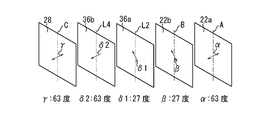
- FIG. 3 is an explanatory diagram for explaining a direction of an optical axis in the display device illustrated in FIG. 1.
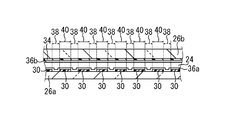
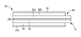
- FIG. 3 is a cross-sectional view of the display device shown in FIG.
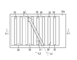
- FIG. 2 is a plan view showing a relationship between an electrode provided on one substrate constituting the display device shown in FIG. 1 and a rubbing direction of an alignment film.
- FIG. 2 is a plan view showing a relationship between an electrode provided on the other substrate constituting the display device shown in FIG. 1 and a rubbing direction of an alignment film.
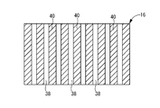
- FIG. 3 is an explanatory diagram illustrating a parallax barrier displayed by a switch liquid crystal panel of the display device illustrated in FIG.
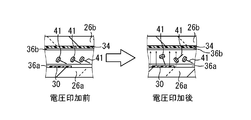
- FIG. 12 is a cross-sectional view of the display device shown in FIG.
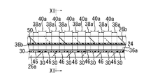
- FIG. 11 is a cross-sectional view of the display device shown in FIG. 9, which is a cross-sectional view in the XI-XI direction of FIG.
- the top view which shows the relationship between the electrode provided in one board
- the top view which shows the relationship between the electrode provided in the other board
- a switch liquid crystal panel is a switch liquid crystal panel capable of displaying a stripe-shaped parallax barrier in which light transmitting portions that transmit light and light shielding portions that block light are alternately formed, A pair of substrates; a twisted nematic liquid crystal layer sandwiched between the pair of substrates; a counter electrode formed on one of the pair of substrates; and a plurality of electrodes formed on the other of the pair of substrates.
- a light shielding part forming electrode that forms the light shielding part in cooperation with the counter electrode when applied, and an alignment film provided on each of the pair of substrates, and the light shielding part forming electrode.
- the rubbing direction of the alignment film on the substrate side on which is formed makes an angle of 45 degrees or less with the length direction of the light shielding portion forming electrode (first configuration relating to the switch liquid crystal panel).
- desired rubbing can be performed on the entire alignment film provided on the substrate side on which the light shielding portion forming electrode is formed.
- the region serving as the light transmitting portion region where the light shielding portion forming electrode is not formed
- the region serving as the light shielding portion light shielding
- the second configuration related to the switch liquid crystal panel is a configuration in which at least one end in the length direction is connected to each other in each of the plurality of light shielding portion forming electrodes in the first configuration related to the switch liquid crystal panel.
- the number of wirings required when applying a voltage is reduced.
- the switch liquid crystal panel can be easily manufactured.
- a third configuration related to the switch liquid crystal panel is the configuration in which the counter electrode is formed over the entire region where the parallax barrier is displayed on the substrate in the first or second configuration related to the switch liquid crystal panel. It is. In such a configuration, the counter electrode can be easily formed.
- a plurality of the light shielding portion forming electrodes are formed on each of the pair of substrates.
- the light shielding part forming electrode formed on one side of the substrate and the light shielding part forming electrode formed on the other side are orthogonal to each other in the projection in the direction in which the pair of substrates face each other. In such a configuration, the direction in which the light transmission part and the light shielding part are arranged can be switched between the vertical direction and the horizontal direction of the substrate.
- a fifth configuration related to the switch liquid crystal panel in the fourth configuration related to the switch liquid crystal panel, there are a plurality of auxiliary electrodes arranged alternately with the light shielding portion forming electrodes on each of the pair of substrates.
- the counter electrode formed on the other substrate to form the light shielding portion in cooperation with the light shielding portion forming electrode formed on one of the substrates is formed on the other substrate. It is the structure comprised including this formed light shielding part formation electrode and this auxiliary electrode. In such a configuration, a configuration for switching the direction in which the light transmitting portion and the light shielding portion are arranged between the vertical direction and the horizontal direction of the substrate can be easily realized.
- the plurality of light shielding part forming electrodes are connected to each other in the length direction.
- the plurality of auxiliary electrodes have a structure in which the other ends in the length direction are connected to each other. In such a configuration, the number of wirings required when applying a voltage is reduced. As a result, the switch liquid crystal panel can be easily manufactured.
- a display device includes a switch liquid crystal panel according to an embodiment of the present invention and a display main panel that displays an image (first configuration related to the display device). .
- the second configuration related to the display device is a configuration in which the display main panel is a transmissive liquid crystal panel in the first configuration related to the display device.
- the display main panel is a transmissive liquid crystal panel in the first configuration related to the display device.
- either the switch liquid crystal panel or the display main panel may be positioned forward. As a result, the degree of freedom in designing the display device can be improved.
- FIG. 1 shows a display device 10 as a first embodiment of the present invention relating to a display device.
- the display device 10 includes a display main panel 12 and a switch liquid crystal panel 14 as a first embodiment of the present invention relating to a switch liquid crystal panel.
- the parallax barrier 16 (see FIG. 6) displayed on the switch liquid crystal panel 14 is displayed by alternately arranging the images for the right eye and the image for the left eye, which are divided into stripes on the display main panel 12.
- the right eye image and the left eye image are shown to the observer.
- the observer can see a stereoscopic image (three-dimensional image) without using glasses.
- the parallax barrier 16 is not displayed on the switch liquid crystal panel 14, if a planar image (two-dimensional image) is displayed on the display main panel 12, the observer can see the planar image.
- the display main panel 12 is a conventionally known transmissive liquid crystal panel.
- the display main panel 12 includes a liquid crystal layer (not shown), an active matrix substrate 18 disposed on one side in the thickness direction of the liquid crystal layer, and a counter substrate disposed on the other side in the thickness direction of the liquid crystal layer. 20.
- the dimension of the active matrix substrate 18 is longer than that of the counter substrate 20 in the lateral direction (left-right direction in FIG. 1).
- polarizing plates 22a and 22b are disposed in a state of being bonded to the opposite side of the liquid crystal layer.
- Each polarizing plate 22a, 22b has a rectangular shape.
- the angle ⁇ formed by the polarizing axis 22a and the reference line A parallel to one side of the polarizing plate 22a is set to 63 degrees.
- An angle ⁇ formed by the polarization axis of the polarizing plate 22b and a reference line B parallel to one side of the polarizing plate 22b is set to 27 degrees.
- the reference line: A and the reference line: B are parallel to each other.
- the active matrix substrate 18 and the counter substrate 20 are each provided with an alignment film.
- Each alignment film has a rectangular shape.
- An angle formed by a reference line extending in the rubbing direction of the alignment film on the active matrix substrate 18 side and a reference line parallel to one side of the alignment film is set to 63 degrees.
- the angle formed by the reference line extending in the rubbing direction of the alignment film on the counter substrate 20 side and the reference line parallel to one side of the alignment film is set to 27 degrees.
- a reference line parallel to one side of the alignment film is parallel to the reference line A.
- image data corresponding to an image to be displayed is input to the active matrix substrate 18 via wiring (not shown) such as FPC (Flexible Printed Circuits).
- FPC Flexible Printed Circuits
- an image is displayed on the display main panel 12.
- the image for the left eye and the image for the right eye, which are divided into stripes are displayed in a display area (not shown) alternately arranged.
- the planar image is displayed in the display area.
- a backlight (not shown) is disposed on one side of the display main panel 12 in the thickness direction.
- a conventionally known backlight can be employed as the backlight.
- a switch liquid crystal panel 14 is disposed on the other side of the display main panel 12 in the thickness direction. As shown in FIG. 3, the switch liquid crystal panel 14 includes a liquid crystal layer 24 and a pair of substrates 26 a and 26 b disposed so as to sandwich the liquid crystal layer 24.
- the liquid crystal layer 24 is a twisted nematic liquid crystal layer.
- Each substrate 26a, 26b is a low alkali glass substrate.
- the size and shape of the substrate 26a are substantially the same as those of the active matrix substrate 18.
- the substrate 26a is bonded to the polarizing plate 22b.
- the size and shape of the substrate 26b are substantially the same as those of the counter substrate 20.
- a polarizing plate 28 (see FIG. 1) is disposed on the side opposite to the liquid crystal layer 24 in a bonded state.
- the polarizing plate 28 has a rectangular shape. As shown in FIG. 2, the angle ⁇ formed by the polarization axis of the polarizing plate 28 and the reference line C parallel to one side of the polarizing plate 28 is set to 27 degrees.
- the reference line C is parallel to the reference line A.
- a plurality of light shielding portion forming electrodes 30 are formed on the substrate 26a.
- FIG. 4 for ease of understanding, only nine light shielding portion forming electrodes 30 are formed, but in reality, a large number of light shielding portion forming electrodes 30 are formed.
- Each light shielding part forming electrode 30 is formed to extend with a substantially constant width dimension in the vertical direction (vertical direction in FIG. 4) of the substrate 26a. Thereby, each light shielding part forming electrode 30 has a vertically long rectangular shape as a whole.
- the plurality of light shielding portion forming electrodes 30 are arranged at equal intervals in the lateral direction of the substrate 26a (left and right direction in FIG. 4). At both ends in the longitudinal direction of each light shielding part forming electrode 30, a connecting electrode 32 is integrally formed extending in the lateral direction of the substrate 26a with a substantially constant width dimension. Thereby, each light shielding part forming electrode 30 and the connecting electrode 32 are electrically connected.
- ITO indium tin oxide
- the counter electrode 34 is formed on the substrate 26b as shown in FIGS.
- the counter electrode 34 is formed over the entire area where the parallax barrier 16 (see FIG. 6) is displayed on the substrate 26b.
- a conventionally known ITO film can be used as the counter electrode 34.
- Alignment films 36a and 36b are formed on the substrates 26a and 26b, respectively.
- Conventionally known polyimide resin films can be adopted as the alignment films 36a and 36b.
- the alignment film 36 a is formed so as to cover the plurality of light shielding part forming electrodes 30 and the connecting electrodes 32.
- the reference line L2 is parallel to the reference line A.
- the alignment film 36 b is formed so as to cover the counter electrode 34.
- the angle ⁇ 2 formed by the reference line L3 extending in the rubbing direction of the alignment film 36b (the direction of the white arrow shown in FIG. 5) and the reference line L4 parallel to one side of the substrate 26b is also shown in FIG. As shown, it is set to 63 degrees.
- the reference line L4 is parallel to the reference line A.
- the parallax barrier 16 as shown in FIG. 6 is displayed on the switch liquid crystal panel 14.
- the parallax barrier 16 is formed by alternately forming light transmitting portions 38 that transmit light and light shielding portions 40 that block light in the lateral direction of the switch liquid crystal panel 14.
- the angle ⁇ 1 formed by the reference line L1 extending in the rubbing direction of the alignment film 36a and the reference line L2 extending in the length direction of the light shielding portion forming electrode 30 is set to 27 degrees. ing.
- desired rubbing can be performed even in the vicinity of the boundary between the region to be the light transmission unit 38 and the region to be the light shielding unit 40.
- a boundary between a region where neither the light shielding portion forming electrode 30 nor the coupling electrode 32 is formed hereinafter referred to as the opening 33
- the opening 33 a boundary between a region where neither the light shielding portion forming electrode 30 nor the coupling electrode 32 is formed.
- the opening 33 a boundary between a region where neither the light shielding portion forming electrode 30 nor the coupling electrode 32 is formed.
- the opening 33 a boundary between a region where neither the light shielding portion forming electrode 30 nor the coupling electrode 32 is formed.
- the opening 33 a boundary between a region where neither the light shielding portion forming electrode 30 nor the coupling
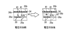
- the orientation of the liquid crystal molecules 41 located in the vicinity of the boundary with the light shielding part forming electrode 30 in the opening 33 is changed when a voltage is applied. That is, as shown in FIG. 7, the liquid crystal molecules 41 located on the light shielding portion forming electrode 30 are perpendicular to the electric field, whereas the openings 33 are connected to the light shielding portion forming electrode 30. An electric field is applied obliquely to the liquid crystal molecules 41 located in the vicinity of the boundary. This is because in the vicinity of the boundary between the opening 33 and the light shielding portion forming electrode 30, the electric field wraps around so as to enter the substrate 26a side.
- the liquid crystal molecules 41 located in the vicinity of the boundary with the light shielding part forming electrode 30 in the opening 33 are not aligned in the rubbing direction, the liquid crystal molecules 41 are directed in the direction in which the electric field wraps around. It will be moved. As a result, the orientation of the liquid crystal molecules 41 is reverse tilt, and there is a problem that a light emitting region is generated.
- Table 1 shows that an angle ⁇ 1 between a reference line L1 extending in the rubbing direction of the alignment film 36a and a reference line L2 extending in the length direction of the light shielding portion forming electrode 30 is within a range of 0 to 90 degrees. It is shown whether or not the light emitting area can be seen when it is changed.
- “ ⁇ ” indicates a case where the light emitting area is not visible
- “X” indicates a case where the light emitting area is visible.
- ⁇ 1 is the smaller of the angles formed by the reference line L1 extending in the rubbing direction of the alignment film 36a and the reference line L2 extending in the length direction of the light shielding portion forming electrode 30. Show.
- an angle ⁇ 1 formed by a reference line L1 extending in the rubbing direction of the alignment film 36a and a reference line L2 extending in the length direction of the light shielding portion forming electrode 30 is set in a range of 0 to 45 degrees. Then, it is possible to prevent the light emitting area from being seen.
- the counter electrode 34 is formed over the entire area where the parallax barrier 16 is displayed. Thereby, formation of the counter electrode 34 becomes easy.
- connection electrodes 32 are integrally formed with respect to both ends in the length direction of the respective light shielding portion forming electrodes 30. Thereby, the number of wirings required when applying a voltage can be reduced. As a result, the switch liquid crystal panel 14 can be easily manufactured.
- a planar image is displayed in a state where no voltage is applied, and a stereoscopic image is displayed in a state where a voltage is applied. Thereby, power consumption can be suppressed.
- the active matrix substrate 18 and the counter substrate 20 of the display main panel 12 are reversed as compared with the display device 10 of the first embodiment.
- the size and shape of the polarizing plate 22 b are substantially the same as those of the active matrix substrate 18. Thereby, it is possible to secure a large adhesion area between the active matrix substrate 18 and the polarizing plate 22b and a bonding area between the polarizing plate 22b and the substrate 26a. As a result, the strength of the display device 42 can be improved.
- the switch liquid crystal panel 44 is different from the display device 10 of the first embodiment. More specifically, as shown in FIG. 12, only one end side in the longitudinal direction of each light shielding portion forming electrode 30 is integrally formed with the connecting electrode 32.
- auxiliary electrodes 46 are formed between two adjacent light shielding part forming electrodes 30, 30 among the plurality of light shielding part forming electrodes 30. ing. Each auxiliary electrode 46 is formed to extend in the vertical direction of the substrate 26a with a substantially constant width dimension. Thereby, each auxiliary electrode 46 has a vertically long rectangular shape as a whole.
- auxiliary electrodes 46 arranged in this manner are each integrally formed with a connecting electrode 48 extending in the lateral direction of the substrate 26a with a substantially constant width dimension at the other end in the length direction. Thereby, each auxiliary electrode 46 and the connection electrode 48 are electrically connected.
- auxiliary electrode 46 and connection electrode 48 As each auxiliary electrode 46 and connection electrode 48, a conventionally known ITO film can be adopted.
- each light shielding portion forming electrode 50 is formed to extend in the lateral direction of the substrate 26b with a substantially constant width dimension.
- each light shielding part forming electrode 50 extends in a direction orthogonal to the length direction of the light shielding part forming electrode 30 on the substrate 26a side.
- Each of the light shielding portion forming electrodes 50 has a horizontally long rectangular shape as a whole.
- the plurality of light shielding portion forming electrodes 50 are arranged at equal intervals in the vertical direction of the substrate 26b.
- a connecting electrode 52 that extends in the longitudinal direction of the substrate 26b with a substantially constant width is integrally formed at one end in the length direction of each light shielding portion forming electrode 50. Thereby, each light shielding part forming electrode 50 and the connecting electrode 52 are electrically connected.
- ITO films can be employed as the respective light shielding part forming electrodes 50 and the connecting electrodes 52.
- Auxiliary electrodes 54 are respectively formed between two adjacent light shielding part forming electrodes 50, 50 among the plurality of light shielding part forming electrodes 50.
- Each auxiliary electrode 54 is formed to extend in the lateral direction of the substrate 26b with a substantially constant width dimension. Thereby, each auxiliary electrode 54 has a horizontally long rectangular shape as a whole.
- the plurality of auxiliary electrodes 54 arranged in this way are integrally formed with a connecting electrode 56 extending in the longitudinal direction of the substrate 26b with a substantially constant width dimension at the other end in the length direction. Thereby, each auxiliary electrode 54 and the connection electrode 56 are electrically connected.
- auxiliary electrode 54 and connection electrode 56 As each auxiliary electrode 54 and connection electrode 56, a conventionally known ITO film can be adopted.
- An angle ⁇ 2 formed by a reference line L5 extending in the rubbing direction of the alignment film 36b on the substrate 26b side where the light shielding part forming electrode 50 is formed and a reference line L6 extending in the length direction of the light shielding part forming electrode 50 is: 27 degrees.
- two types of parallax barriers 16a and 16b can be displayed by applying a driving voltage to the switch liquid crystal panel 44.
- the parallax barrier 16a as shown in FIG. 14 is displayed on the switch liquid crystal panel 44.
- the light transmission portions 38a and the light shielding portions 40a are formed so as to be alternately arranged in the long side direction of the substrates 26a and 26b (left and right directions in FIGS. 12 and 13).
- a drive voltage is applied to the switch liquid crystal panel 44, and all the electrodes on the substrate 26b side (a plurality of light shielding portion forming electrodes 50 and connecting electrodes 52, a plurality of auxiliary electrodes 54 and connecting electrodes 56), and the substrate 26a.
- the plurality of auxiliary electrodes 46 and the connection electrodes 48 provided on the side are set to the same potential (for example, 0 V), and the plurality of light shielding part forming electrodes 30 and the connection electrodes 32 are all provided on the substrate 26b.
- a plurality of light shielding part forming electrodes 50 and connecting electrodes 52, and a plurality of auxiliary electrodes 54 and connecting electrodes 56) or a plurality of auxiliary electrodes 46 and connecting electrodes 48 provided on the substrate 26a are different in potential ( For example, when 5 V), the orientation of the liquid crystal molecules located between the light shielding part forming electrode 30 and the counter electrode 34b (see FIG. 13) changes. As a result, a stripe-shaped parallax barrier 16 a as shown in FIG.
- the plurality of light shielding portion forming electrodes 50 and the connection electrodes 52, and the plurality of auxiliary electrodes 54 and the connection electrodes 56 act as the counter electrodes 34b. It has become.
- the reference line L1 extending in the rubbing direction of the alignment film 36a (the direction of the white arrow in FIG. 12) and the reference line L2 extending in the length direction of the light shielding portion forming electrode 30 are used.
- Angle: ⁇ 1 is set to 27 degrees.
- the parallax barrier 16b As shown in FIG. 15 is displayed will be described.
- the light transmitting portions 38b and the light shielding portions 40b are formed so as to be alternately arranged in the short side direction (vertical direction in FIGS. 12 and 13) of the substrates 26a and 26b.
- the switch liquid crystal panel 44 By applying a driving voltage to the switch liquid crystal panel 44, all electrodes on the substrate 26a side (a plurality of light shielding portion forming electrodes 30 and connection electrodes 32, a plurality of auxiliary electrodes 46 and connection electrodes 48), and a substrate 26b.
- the plurality of auxiliary electrodes 54 and the connection electrodes 56 on the side are set to the same potential (for example, 0 V), and the plurality of light shielding portion forming electrodes 50 and the connection electrodes 52 on the substrate 26b side
- the light shielding portion forming electrode 30 and the connecting electrode 32, the plurality of auxiliary electrodes 46 and the connecting electrodes 48), and the plurality of auxiliary electrodes 54 and the connecting electrodes 56 on the substrate 26b side for example, 5 V.
- the orientation of the liquid crystal molecules located between the light shielding part forming electrode 50 and the counter electrode 34a changes.
- a stripe-shaped parallax barrier 16 b as shown in FIG. 15 is displayed on the switch liquid crystal panel 44.
- the plurality of light shielding portion forming electrodes 30 and the coupling electrodes 32, and the plurality of auxiliary electrodes 46 and the coupling electrodes 48 function as the counter electrodes 34a. It has become.
- the reference line L5 extending in the rubbing direction of the alignment film 36b (the direction of the white arrow in FIG. 13) and the reference line L6 extending in the length direction of the light shielding portion forming electrode 50 are used.
- Angle: ⁇ 2 is set to 27 degrees.
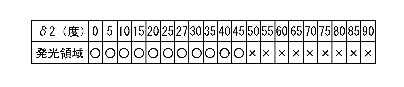
- Table 2 shows that an angle ⁇ 2 formed by a reference line L5 extending in the rubbing direction of the alignment film 36b and a reference line L6 extending in the length direction of the light shielding portion forming electrode 50 is within a range of 0 to 90 degrees. It is shown whether or not the light emitting area can be seen when it is changed.
- “ ⁇ ” indicates a case where the light emitting area is not visible
- “X” indicates a case where the light emitting area is visible.
- ⁇ 2 is the smaller of the angles formed by the reference line L5 extending in the rubbing direction of the alignment film 36b and the reference line L6 extending in the length direction of the light shielding portion forming electrode 50. Show.
- the angle ⁇ 2 formed by the reference line L5 extending in the rubbing direction of the alignment film 36b and the reference line L6 extending in the length direction of the light shielding portion forming electrode 50 is set in the range of 0 to 45 degrees. Then, it is possible to prevent the light emitting area from being seen.
- a stereoscopic image is displayed both when the long side direction of the substrates 26a and 26b is set to the vertical direction and when the short side direction is set to the vertical direction (the stereoscopic image is viewed by an observer). To show).
- a plurality of auxiliary electrodes 46 and 54 are connected by connecting electrodes 48 and 56, and a plurality of light shielding part forming electrodes 30 and 50 are connected by connecting electrodes 32 and 52. Thereby, the number of wirings required when applying a voltage can be reduced.
- the switch liquid crystal panels 14 and 44 may be disposed between the display main panel 12 and the backlight.
- a plasma display panel PDP
- an organic EL panel or the like may be employed as the display main panel.
- the present invention can also be applied to a display device in which different images are displayed when the display screen is viewed from the left oblique direction and when viewed from the right oblique direction.
Landscapes
- Physics & Mathematics (AREA)
- General Physics & Mathematics (AREA)
- Optics & Photonics (AREA)
- Nonlinear Science (AREA)
- Mathematical Physics (AREA)
- Chemical & Material Sciences (AREA)
- Crystallography & Structural Chemistry (AREA)
- Liquid Crystal (AREA)
Abstract
Description
[第一の実施形態]
図1には、表示装置に関する本発明の第一の実施形態としての表示装置10が示されている。表示装置10は、表示用メインパネル12と、スイッチ液晶パネルに関する本発明の第一の実施形態としてのスイッチ液晶パネル14とを備えている。表示装置10においては、表示用メインパネル12においてストライプ状に分割された右眼用画像と左眼用画像を交互に並べて表示し、スイッチ液晶パネル14に表示した視差バリア16(図6参照)を介して、右眼用画像と左目用画像を観察者に見せるようになっている。これにより、観察者の右眼には右眼用画像のみが届き、観察者の左眼には左眼用画像のみが届く。その結果、観察者は、メガネを使用せずに、立体画像(3次元画像)を見ることができる。また、スイッチ液晶パネル14に視差バリア16を表示しない場合において、表示用メインパネル12に平面画像(2次元画像)を表示すれば、観察者は平面画像を見ることができるようになっている。

続いて、表示装置に関する本発明の第二の実施形態について、図9~15に基づいて、説明する。なお、以下の説明において、第一の実施形態と同様な構造とされた部材及び部位については、図中に、第一の実施形態と同一の符号を付すことにより、それらの詳細な説明を省略する。
Claims (8)
- 光を透過させる光透過部と光を遮断する遮光部とが交互に形成されたストライプ状の視差バリアを表示可能なスイッチ液晶パネルであって、
一対の基板と、
該一対の基板間に挟まれたツイストネマティック型の液晶層と、
前記一対の基板の一方に形成された対向電極と、
前記一対の基板の他方に複数形成されて、電圧が印加された際に前記対向電極と協働して前記遮光部を形成する遮光部形成用電極と、
前記一対の基板のそれぞれに設けられた配向膜と
を備えており、
前記遮光部形成用電極が形成された基板側の前記配向膜のラビング方向が、該遮光部形成用電極の長さ方向と45度以下の角度を為している、スイッチ液晶パネル。 - 複数の前記遮光部形成用電極のそれぞれにおいて、少なくとも長さ方向一端同士が相互に連結されている、請求項1に記載のスイッチ液晶パネル。
- 前記対向電極が、前記基板において前記視差バリアが表示される領域の全体に亘って形成されている、請求項1又は2に記載のスイッチ液晶パネル。
- 前記一対の基板のそれぞれに対して、複数の前記遮光部形成用電極が形成されており、
前記一対の基板の一方に形成された前記遮光部形成用電極と、他方に形成された該遮光部形成用電極とが、該一対の基板が対向する方向の投影において直交している請求項1又は2に記載のスイッチ液晶パネル。 - 前記一対の基板のそれぞれに対して、前記遮光部形成用電極と交互に並ぶように配置される補助電極が複数形成されており、
一方の該基板に形成された該遮光部形成用電極と協働して前記遮光部を形成するために他方の該基板に形成された前記対向電極が、他方の該基板に形成された該遮光部形成用電極と該補助電極を含んで構成されている、請求項4に記載のスイッチ液晶パネル。 - 前記一対の基板のそれぞれにおいて、
複数の前記遮光部形成用電極は、長さ方向一端同士が相互に連結されており、
複数の前記補助電極は、長さ方向他端同士が相互に連結されている、請求項5に記載のスイッチ液晶パネル。 - 請求項1~6の何れか1項に記載のスイッチ液晶パネルと、
画像を表示する表示用メインパネルと
を備えている、表示装置。 - 前記表示用メインパネルが透過型液晶パネルである、請求項7に記載の表示装置。
Priority Applications (4)
| Application Number | Priority Date | Filing Date | Title |
|---|---|---|---|
| US13/812,937 US9041872B2 (en) | 2010-07-29 | 2011-07-25 | Switching liquid crystal panel and display device |
| CN2011800372189A CN103038702A (zh) | 2010-07-29 | 2011-07-25 | 开关液晶面板和显示装置 |
| AU2011283761A AU2011283761A1 (en) | 2010-07-29 | 2011-07-25 | Switch liquid crystal panel and display device |
| JP2012526483A JPWO2012014827A1 (ja) | 2010-07-29 | 2011-07-25 | スイッチ液晶パネル及び表示装置 |
Applications Claiming Priority (2)
| Application Number | Priority Date | Filing Date | Title |
|---|---|---|---|
| JP2010170943 | 2010-07-29 | ||
| JP2010-170943 | 2010-07-29 |
Publications (1)
| Publication Number | Publication Date |
|---|---|
| WO2012014827A1 true WO2012014827A1 (ja) | 2012-02-02 |
Family
ID=45530035
Family Applications (1)
| Application Number | Title | Priority Date | Filing Date |
|---|---|---|---|
| PCT/JP2011/066793 Ceased WO2012014827A1 (ja) | 2010-07-29 | 2011-07-25 | スイッチ液晶パネル及び表示装置 |
Country Status (5)
| Country | Link |
|---|---|
| US (1) | US9041872B2 (ja) |
| JP (1) | JPWO2012014827A1 (ja) |
| CN (1) | CN103038702A (ja) |
| AU (1) | AU2011283761A1 (ja) |
| WO (1) | WO2012014827A1 (ja) |
Cited By (3)
| Publication number | Priority date | Publication date | Assignee | Title |
|---|---|---|---|---|
| CN102929023A (zh) * | 2012-10-26 | 2013-02-13 | 南京华日液晶显示技术有限公司 | 利用lcd制作2d/3d显示切换视差障栅的方法 |
| CN103576328A (zh) * | 2012-08-06 | 2014-02-12 | 韩国电子通信研究院 | 具有2d/3d 模式转换的基于分段视差屏障的显示设备及方法 |
| WO2015162995A1 (ja) * | 2014-04-22 | 2015-10-29 | シャープ株式会社 | 立体表示装置 |
Families Citing this family (1)
| Publication number | Priority date | Publication date | Assignee | Title |
|---|---|---|---|---|
| US10725319B2 (en) * | 2016-01-13 | 2020-07-28 | Sharp Kabushiki Kaisha | Display device and liquid crystal panel driving method |
Citations (3)
| Publication number | Priority date | Publication date | Assignee | Title |
|---|---|---|---|---|
| JP2003279924A (ja) * | 2002-03-22 | 2003-10-02 | Ricoh Co Ltd | 光路偏向装置及び画像表示装置 |
| JP2005134663A (ja) * | 2003-10-30 | 2005-05-26 | Asahi Glass Co Ltd | 多機能表示装置および同装置に用いられるスリットマスク形成用のスイッチング液晶パネル |
| JP2006047507A (ja) * | 2004-08-02 | 2006-02-16 | Sharp Corp | 表示装置及び表示方法 |
Family Cites Families (7)
| Publication number | Priority date | Publication date | Assignee | Title |
|---|---|---|---|---|
| JPH07261119A (ja) | 1994-03-22 | 1995-10-13 | Sanyo Electric Co Ltd | 立体映像表示装置 |
| JP4050065B2 (ja) | 2002-02-05 | 2008-02-20 | 株式会社リコー | 画像表示装置 |
| JP2004264760A (ja) | 2003-03-04 | 2004-09-24 | Sanyo Electric Co Ltd | 立体映像表示装置 |
| US7898602B2 (en) * | 2005-04-08 | 2011-03-01 | Sharp Kabushiki Kaisha | Display apparatus |
| US20100321621A1 (en) * | 2007-11-29 | 2010-12-23 | Ryo Kikuchi | Display device |
| JP5246746B2 (ja) * | 2008-01-21 | 2013-07-24 | 株式会社ジャパンディスプレイウェスト | 電気光学装置、電気光学装置の製造方法及び電子機器 |
| JP5705420B2 (ja) * | 2009-07-03 | 2015-04-22 | 株式会社ジャパンディスプレイ | 液晶パララックスバリア、表示装置及び液晶表示装置 |
-
2011
- 2011-07-25 US US13/812,937 patent/US9041872B2/en active Active
- 2011-07-25 WO PCT/JP2011/066793 patent/WO2012014827A1/ja not_active Ceased
- 2011-07-25 CN CN2011800372189A patent/CN103038702A/zh active Pending
- 2011-07-25 AU AU2011283761A patent/AU2011283761A1/en not_active Abandoned
- 2011-07-25 JP JP2012526483A patent/JPWO2012014827A1/ja active Pending
Patent Citations (3)
| Publication number | Priority date | Publication date | Assignee | Title |
|---|---|---|---|---|
| JP2003279924A (ja) * | 2002-03-22 | 2003-10-02 | Ricoh Co Ltd | 光路偏向装置及び画像表示装置 |
| JP2005134663A (ja) * | 2003-10-30 | 2005-05-26 | Asahi Glass Co Ltd | 多機能表示装置および同装置に用いられるスリットマスク形成用のスイッチング液晶パネル |
| JP2006047507A (ja) * | 2004-08-02 | 2006-02-16 | Sharp Corp | 表示装置及び表示方法 |
Cited By (3)
| Publication number | Priority date | Publication date | Assignee | Title |
|---|---|---|---|---|
| CN103576328A (zh) * | 2012-08-06 | 2014-02-12 | 韩国电子通信研究院 | 具有2d/3d 模式转换的基于分段视差屏障的显示设备及方法 |
| CN102929023A (zh) * | 2012-10-26 | 2013-02-13 | 南京华日液晶显示技术有限公司 | 利用lcd制作2d/3d显示切换视差障栅的方法 |
| WO2015162995A1 (ja) * | 2014-04-22 | 2015-10-29 | シャープ株式会社 | 立体表示装置 |
Also Published As
| Publication number | Publication date |
|---|---|
| US20130128163A1 (en) | 2013-05-23 |
| AU2011283761A1 (en) | 2013-02-21 |
| US9041872B2 (en) | 2015-05-26 |
| JPWO2012014827A1 (ja) | 2013-09-12 |
| CN103038702A (zh) | 2013-04-10 |
Similar Documents
| Publication | Publication Date | Title |
|---|---|---|
| JP5550165B2 (ja) | 電子映像機器 | |
| KR101113066B1 (ko) | 패러렉스 베리어 액정패널 및 이를 이용한입체영상표시장치 | |
| JP2004302409A (ja) | 液晶表示パネル、および液晶表示装置 | |
| CN105745570A (zh) | 显示装置 | |
| JP2015045665A (ja) | 立体表示装置 | |
| KR101915623B1 (ko) | 액정 렌즈 패널 및 이를 구비하는 표시 장치 | |
| CN102375272A (zh) | 光屏障装置和显示单元 | |
| CN102375265A (zh) | 显示设备和光阻挡装置 | |
| US9105224B2 (en) | Stereoscopic display device | |
| JP2011169949A (ja) | 3次元画像表示装置 | |
| JP6125027B2 (ja) | 立体表示装置 | |
| WO2014136610A1 (ja) | 立体表示装置 | |
| WO2012014827A1 (ja) | スイッチ液晶パネル及び表示装置 | |
| US9459462B2 (en) | Stereoscopic display device | |
| JP5587272B2 (ja) | 画像表示装置 | |
| JP5669945B2 (ja) | 立体表示装置 | |
| JP2015014670A (ja) | 液晶表示装置 | |
| US20130265510A1 (en) | Three-dimensional display device and active optical element thereof | |
| JP2013045064A (ja) | 表示装置、バリア装置、位相差フィルム、および電子機器 | |
| CN105759436B (zh) | 裸眼三维显示系统和折射率调节装置 | |
| KR102434032B1 (ko) | 배리어패널 및 이를 포함하는 표시장치 | |
| WO2012153689A1 (ja) | 表示装置 | |
| JP2008180918A (ja) | 液晶表示装置 | |
| WO2012137471A1 (ja) | 液晶パネル及びそれを備えた表示装置 | |
| WO2012132330A1 (ja) | 液晶パネル及びそれを備えた表示装置 |
Legal Events
| Date | Code | Title | Description |
|---|---|---|---|
| WWE | Wipo information: entry into national phase |
Ref document number: 201180037218.9 Country of ref document: CN |
|
| 121 | Ep: the epo has been informed by wipo that ep was designated in this application |
Ref document number: 11812417 Country of ref document: EP Kind code of ref document: A1 |
|
| WWE | Wipo information: entry into national phase |
Ref document number: 2012526483 Country of ref document: JP |
|
| NENP | Non-entry into the national phase |
Ref country code: DE |
|
| WWE | Wipo information: entry into national phase |
Ref document number: 13812937 Country of ref document: US |
|
| ENP | Entry into the national phase |
Ref document number: 2011283761 Country of ref document: AU Date of ref document: 20110725 Kind code of ref document: A |
|
| 122 | Ep: pct application non-entry in european phase |
Ref document number: 11812417 Country of ref document: EP Kind code of ref document: A1 |