WO2012014819A1 - 表示装置 - Google Patents
表示装置 Download PDFInfo
- Publication number
- WO2012014819A1 WO2012014819A1 PCT/JP2011/066747 JP2011066747W WO2012014819A1 WO 2012014819 A1 WO2012014819 A1 WO 2012014819A1 JP 2011066747 W JP2011066747 W JP 2011066747W WO 2012014819 A1 WO2012014819 A1 WO 2012014819A1
- Authority
- WO
- WIPO (PCT)
- Prior art keywords
- light source
- sensor
- period
- signal
- circuit
- Prior art date
- Legal status (The legal status is an assumption and is not a legal conclusion. Google has not performed a legal analysis and makes no representation as to the accuracy of the status listed.)
- Ceased
Links
Images














Classifications
-
- G—PHYSICS
- G09—EDUCATION; CRYPTOGRAPHY; DISPLAY; ADVERTISING; SEALS
- G09G—ARRANGEMENTS OR CIRCUITS FOR CONTROL OF INDICATING DEVICES USING STATIC MEANS TO PRESENT VARIABLE INFORMATION
- G09G3/00—Control arrangements or circuits, of interest only in connection with visual indicators other than cathode-ray tubes
- G09G3/20—Control arrangements or circuits, of interest only in connection with visual indicators other than cathode-ray tubes for presentation of an assembly of a number of characters, e.g. a page, by composing the assembly by combination of individual elements arranged in a matrix no fixed position being assigned to or needed to be assigned to the individual characters or partial characters
- G09G3/34—Control arrangements or circuits, of interest only in connection with visual indicators other than cathode-ray tubes for presentation of an assembly of a number of characters, e.g. a page, by composing the assembly by combination of individual elements arranged in a matrix no fixed position being assigned to or needed to be assigned to the individual characters or partial characters by control of light from an independent source
- G09G3/3406—Control of illumination source
-
- G—PHYSICS
- G06—COMPUTING OR CALCULATING; COUNTING
- G06F—ELECTRIC DIGITAL DATA PROCESSING
- G06F3/00—Input arrangements for transferring data to be processed into a form capable of being handled by the computer; Output arrangements for transferring data from processing unit to output unit, e.g. interface arrangements
- G06F3/01—Input arrangements or combined input and output arrangements for interaction between user and computer
- G06F3/03—Arrangements for converting the position or the displacement of a member into a coded form
- G06F3/041—Digitisers, e.g. for touch screens or touch pads, characterised by the transducing means
- G06F3/0412—Digitisers structurally integrated in a display
-
- G—PHYSICS
- G06—COMPUTING OR CALCULATING; COUNTING
- G06F—ELECTRIC DIGITAL DATA PROCESSING
- G06F3/00—Input arrangements for transferring data to be processed into a form capable of being handled by the computer; Output arrangements for transferring data from processing unit to output unit, e.g. interface arrangements
- G06F3/01—Input arrangements or combined input and output arrangements for interaction between user and computer
- G06F3/03—Arrangements for converting the position or the displacement of a member into a coded form
- G06F3/041—Digitisers, e.g. for touch screens or touch pads, characterised by the transducing means
- G06F3/042—Digitisers, e.g. for touch screens or touch pads, characterised by the transducing means by opto-electronic means
-
- G—PHYSICS
- G09—EDUCATION; CRYPTOGRAPHY; DISPLAY; ADVERTISING; SEALS
- G09G—ARRANGEMENTS OR CIRCUITS FOR CONTROL OF INDICATING DEVICES USING STATIC MEANS TO PRESENT VARIABLE INFORMATION
- G09G3/00—Control arrangements or circuits, of interest only in connection with visual indicators other than cathode-ray tubes
- G09G3/20—Control arrangements or circuits, of interest only in connection with visual indicators other than cathode-ray tubes for presentation of an assembly of a number of characters, e.g. a page, by composing the assembly by combination of individual elements arranged in a matrix no fixed position being assigned to or needed to be assigned to the individual characters or partial characters
- G09G3/34—Control arrangements or circuits, of interest only in connection with visual indicators other than cathode-ray tubes for presentation of an assembly of a number of characters, e.g. a page, by composing the assembly by combination of individual elements arranged in a matrix no fixed position being assigned to or needed to be assigned to the individual characters or partial characters by control of light from an independent source
- G09G3/36—Control arrangements or circuits, of interest only in connection with visual indicators other than cathode-ray tubes for presentation of an assembly of a number of characters, e.g. a page, by composing the assembly by combination of individual elements arranged in a matrix no fixed position being assigned to or needed to be assigned to the individual characters or partial characters by control of light from an independent source using liquid crystals
- G09G3/3611—Control of matrices with row and column drivers
- G09G3/3648—Control of matrices with row and column drivers using an active matrix
-
- G—PHYSICS
- G09—EDUCATION; CRYPTOGRAPHY; DISPLAY; ADVERTISING; SEALS
- G09G—ARRANGEMENTS OR CIRCUITS FOR CONTROL OF INDICATING DEVICES USING STATIC MEANS TO PRESENT VARIABLE INFORMATION
- G09G2330/00—Aspects of power supply; Aspects of display protection and defect management
- G09G2330/02—Details of power systems and of start or stop of display operation
- G09G2330/025—Reduction of instantaneous peaks of current
-
- G—PHYSICS
- G09—EDUCATION; CRYPTOGRAPHY; DISPLAY; ADVERTISING; SEALS
- G09G—ARRANGEMENTS OR CIRCUITS FOR CONTROL OF INDICATING DEVICES USING STATIC MEANS TO PRESENT VARIABLE INFORMATION
- G09G2360/00—Aspects of the architecture of display systems
- G09G2360/14—Detecting light within display terminals, e.g. using a single or a plurality of photosensors
- G09G2360/141—Detecting light within display terminals, e.g. using a single or a plurality of photosensors the light conveying information used for selecting or modulating the light emitting or modulating element
- G09G2360/142—Detecting light within display terminals, e.g. using a single or a plurality of photosensors the light conveying information used for selecting or modulating the light emitting or modulating element the light being detected by light detection means within each pixel
Definitions
- the present invention relates to a display device with a photosensor having a photodetection element such as a photodiode, and more particularly to a display device having a light source different from a display light source as a light source for detection light.
- a display device with a photosensor that can detect the brightness of external light or capture an image of an object close to the display by providing a photodetection element such as a photodiode in the pixel.
- a display device with an optical sensor is assumed to be used as a display device for bidirectional communication or a display device with a touch panel function.
- a backlight combining different light sources that respectively emit visible light and invisible light is used, and these light sources are turned on at different timings, so that an object can be displayed independently of image display.
- a configuration for performing position detection is disclosed in, for example, Japanese Patent Application Laid-Open No. 2005-275644.
- the light source for invisible light is driven in accordance with the timing at which the light sensor detects light. It will be. In this case, there has been a problem that when the light source for invisible light is turned on, a voltage drop may occur instantaneously in the backlight.
- an object of the present invention is to suppress a voltage drop when an invisible light source is turned on in a display device with an optical sensor having both a visible light source and an invisible light source.
- the display device disclosed herein includes an active matrix substrate, a photosensor provided in a pixel region of the active matrix substrate, a visible light source for displaying an image in the pixel region, and reflected light by the photosensor.
- a non-visible light source for detection and a light source control circuit for controlling turning on and off of the visible light source and the non-visible light source, and the light source control circuit turns on the non-visible light source.
- the drive current supplied to the visible light source is configured to be smaller than the drive current supplied to the visible light source when the invisible light source is turned off.
- a display device with an optical sensor that has both a visible light source and a non-visible light source and suppresses a voltage drop when the non-visible light source is turned on.
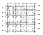
- FIG. 2 is a diagram showing an arrangement of sensor pixel circuits in a display panel included in the display device shown in FIG. 1.
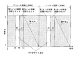
- FIG. 2 is a diagram illustrating backlight lighting and extinguishing timings when the display device illustrated in FIG. 1 is driven once, and resetting and reading timings for sensor pixel circuits.
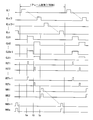
- FIG. 2 is a signal waveform diagram of the display panel when the display device shown in FIG. 1 is driven once.
- FIG. 1 shows schematic structure of the sensor pixel circuit contained in the display apparatus shown in FIG. 1 is a circuit diagram of a sensor pixel circuit according to a first embodiment of the present invention.
- FIG. 1 is a circuit diagram showing an arrangement of sensor pixel circuits in a display panel included in the display device shown in FIG. 1.
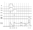
- FIG. 2 is a diagram illustrating backlight lighting and extinguishing timings when the display device illustrated in FIG. 1 is driven once, and resetting and reading timings for sensor pixel circuits.
- FIG. 2 is a signal waveform diagram of
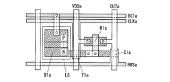
- FIG. 7 is a layout diagram of the sensor pixel circuit shown in FIG. 6. It is a figure which shows operation
- FIG. 7 is a signal waveform diagram of the sensor pixel circuit shown in FIG. 6.
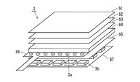
- FIG. 10 is an exploded perspective view illustrating a configuration example of the backlight.
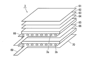
- FIG. 11 is an exploded perspective view illustrating a configuration example of the backlight.
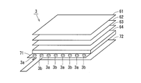
- FIG. 12 is an exploded perspective view illustrating a configuration example of the backlight.
- FIG. 13 is an exploded perspective view illustrating a configuration example of the backlight.
- FIG. 14 is an exploded perspective view illustrating a configuration example of the backlight.
- FIG. 15 is a cross-sectional view showing a schematic configuration of the backlight shown in FIG. FIG.
- FIG. 16 is a signal waveform diagram showing an example of the drive current output from the backlight control circuit to the backlight.
- FIG. 17 is a signal waveform diagram showing an example of drive current output from the backlight control circuit to the backlight.
- FIG. 18 is a signal waveform diagram illustrating an example of a drive current output from the backlight control circuit to the backlight.
- FIG. 19 is a signal waveform diagram showing an example of drive current output from the backlight control circuit to the backlight.
- FIG. 20 is a signal waveform diagram of the drive current in the case where the white LED continues to be lit even during the lighting period of the infrared LED as a comparative example to the examples shown in FIGS.
- FIG. 21 is a circuit diagram showing a schematic configuration of the backlight control circuit.
- FIG. 22 is a timing chart showing the operation of the backlight control circuit.
- FIG. 23A is a comparative example of the backlight control circuit according to the present embodiment shown in FIG. 21, and is a configuration example of a lighting control circuit for temporarily turning on the infrared LED while always turning on the white LED.
- FIG. 23B is a comparative example of the backlight control circuit according to the present embodiment shown in FIG. 21, and is a configuration example of a lighting control circuit for temporarily lighting the infrared LED while always lighting the white LED.
- FIG. FIG. 6 is a circuit diagram of a sensor pixel circuit according to a second embodiment of the present invention.
- FIG. 25 is a layout diagram of the sensor pixel circuit shown in FIG. 24.
- FIG. 24 is a layout diagram of the sensor pixel circuit shown in FIG. 24.
- FIG. 25 is a diagram showing an operation of the sensor pixel circuit shown in FIG. 24.
- FIG. 25 is a signal waveform diagram of the sensor pixel circuit shown in FIG. 24.
- 6 is a circuit diagram of a sensor pixel circuit according to a first modification of the first embodiment.
- FIG. It is a circuit diagram of the sensor pixel circuit concerning the 2nd modification of a 1st embodiment. It is a circuit diagram of the sensor pixel circuit concerning the 3rd modification of a 1st embodiment. It is a circuit diagram of the sensor pixel circuit concerning the 4th modification of a 1st embodiment. It is a circuit diagram of the sensor pixel circuit concerning the 5th modification of a 1st embodiment. It is a figure which shows operation
- FIG. 28C is a signal waveform diagram of the sensor pixel circuit shown in FIG. 28C. It is a figure which shows operation
- a display device includes: An active matrix substrate; A photosensor provided in a pixel region of the active matrix substrate; A visible light source for displaying an image in the pixel region; An invisible light source for detecting reflected light by the optical sensor; A light source control circuit for controlling turning on and off of the visible light source and the invisible light source, The light source control circuit reduces the drive current supplied to the visible light source during the period when the invisible light source is turned on, less than the drive current supplied to the visible light source when the invisible light source is turned off. (First configuration).
- the sum of the power of the invisible light source and the power of the visible light source when the invisible light source is turned on is the sum of the power of the invisible light source and the visible light source when the invisible light source is turned off. It can be set as the structure equal to the sum with electric power (2nd structure).
- the length of the period during which the drive current supplied to the visible light source is reduced may be longer than the lighting period of the invisible light source (third configuration).
- the light source control circuit may be configured to start a period in which the drive current supplied to the visible light source is reduced before the invisible light source is turned on (fourth configuration).
- the light source control circuit is A power supply control circuit connected to the first terminal of the visible light source and the first terminal of the invisible light source, and supplying a constant voltage to the visible light source and the invisible light source; A first switching element connected between a second terminal of the visible light source and a resistor; It is good also as a structure provided with the 2nd switching element connected between the 2nd terminal of the said invisible light source, and resistance (5th structure).
- the visible light source may be a white LED (sixth configuration).
- the invisible light source may be an infrared LED (seventh configuration).
- a sensor driving circuit for supplying a sensor driving signal to the optical sensor;
- An amplifier circuit that amplifies the signal read from the photosensor in accordance with the sensor drive signal and outputs it as a photosensor signal;
- a signal processing circuit that processes the optical sensor signal output from the amplifier circuit;
- the light sensor includes In accordance with the sensor drive signal, a first sensor pixel circuit that accumulates charges according to the amount of received light during the accumulation period when the invisible light source is turned on, and outputs a sensor signal according to the accumulated charges when the readout period comes;
- a second sensor pixel circuit that accumulates charges according to the amount of received light during the accumulation period when the invisible light source is extinguished according to the sensor drive signal, and outputs a sensor signal according to the accumulated charges when the readout period arrives
- the signal processing circuit may be configured to obtain a difference between a sensor signal output from the first sensor pixel circuit and a sensor signal output from the second sensor pixel circuit (eighth configuration).
- Each of the first and second sensor pixel circuits includes: One light receiving element; One storage node that accumulates charges according to the detected light quantity; A read transistor having a control terminal electrically connectable to the storage node; A holding switching element that is provided on a path of a current flowing through the light receiving element and that is turned on / off in accordance with the control signal may be included (a ninth structure).
- the holding switching element is provided between the storage node and one end of the light receiving element, The other end of the light receiving element may be connected to a reset line (tenth configuration).
- the first and second sensor pixel circuits share one light receiving element, One end of the light receiving element may be connected to one end of a holding switching element included in each of the first and second sensor pixel circuits, and the other end may be connected to the reset line (11th configuration). .
- a counter substrate facing the active matrix substrate A configuration further including a liquid crystal sandwiched between the active matrix substrate and the counter substrate may be employed (a twelfth configuration).
- the display device according to the present invention is not limited to the liquid crystal display device, and is an active matrix.
- the present invention can be applied to any display device using a substrate.
- the display device according to the present invention includes a touch panel display device that performs an input operation by detecting an object close to the screen by using an optical sensor, and a display for bidirectional communication including a display function and an imaging function. Use as a device is assumed.
- each drawing referred to below shows only the main members necessary for explaining the present invention in a simplified manner among the constituent members of the embodiment of the present invention for convenience of explanation. Therefore, the display device according to the present invention can include arbitrary constituent members that are not shown in the drawings referred to in this specification. Moreover, the dimension of the member in each figure does not represent the dimension of an actual structural member, the dimension ratio of each member, etc. faithfully.
- FIG. 1 is a block diagram showing a configuration of a display device according to the first embodiment of the present invention.
- the display device shown in FIG. 1 includes a display control circuit 1, a display panel 2, a backlight 3, and a backlight control circuit 13 (light source control circuit).
- the display panel 2 includes a pixel region 4, a gate driver circuit 5, a source driver circuit 6 (amplifier circuit), and a sensor row driver circuit 7 (sensor drive circuit).
- the pixel region 4 includes a plurality of display pixel circuits 8 and a plurality of sensor pixel circuits 9 (photosensors).
- This display device has a function of displaying an image on the display panel 2 and a function of detecting light incident on the display panel 2.
- x is an integer of 2 or more
- y is a multiple of 3
- m and n are even numbers
- the frame rate of the display device is 60 frames / second.
- the video signal Vin and the timing control signal Cin are supplied from the outside to the display device shown in FIG. Based on these signals, the display control circuit 1 outputs a video signal VS and control signals CSg, CSs, and CSr to the display panel 2 and outputs a control signal CSb to the backlight control circuit 13.
- the video signal VS may be the same as the video signal Vin, or may be a signal obtained by performing signal processing on the video signal Vin.
- the backlight 3 is provided on the back side of the display panel 2 and irradiates the back of the display panel 2 with light.
- the backlight 3 includes a white LED 3a as a visible light source and an infrared LED (indicated as IR-LED in FIG. 1) 3b as a non-visible light source.
- the visible light source (here, the white LED 3 a) is a light source used for displaying an image in the pixel region 4.
- the non-visible light source (infrared LED 3b here) is a light source that emits light in a wavelength region other than visible light. The light emitted from the non-visible light source is reflected by a finger or a touch pen touching the surface of the display panel 2 and is incident on the sensor pixel circuit 9, whereby the touch position can be detected.
- the white LED 3a is used as the visible light source and the infrared LED 3b is used as the invisible light source.
- other light sources may be used.
- light sources other than LEDs can be used as these light sources.
- light emitted from the visible light source may include light in a wavelength region other than visible light.
- the emitted light from the non-visible light source preferably does not include a wavelength component in the visible region, but the wavelength component in the visible region does not have to be zero.
- the backlight control circuit 13 supplies the white LED 3a with a drive current CS3a that controls turning on / off the white LED 3a.
- the backlight control circuit 13 supplies a drive current CS3b for controlling the turning on / off of the infrared LED 3b.
- the on / off timing of the white LED 3a and the infrared LED 3b will be described in detail later.
- (x ⁇ y) display pixel circuits 8 and (n ⁇ m / 2) sensor pixel circuits 9 are two-dimensionally arranged. More specifically, the pixel region 4 is provided with x gate lines GL1 to GLx and y source lines SL1 to SLy.
- the gate lines GL1 to GLx are arranged in parallel to each other, and the source lines SL1 to SLy are arranged in parallel to each other so as to be orthogonal to the gate lines GL1 to GLx.
- the (x ⁇ y) display pixel circuits 8 are arranged in the vicinity of intersections of the gate lines GL1 to GLx and the source lines SL1 to SLy.
- Each display pixel circuit 8 is connected to one gate line GL and one source line SL.
- the display pixel circuit 8 is classified into red display, green display, and blue display. These three types of display pixel circuits 8 are arranged side by side in the extending direction of the gate lines GL1 to GLx, and constitute one color pixel.
- n clock lines CLK1 to CLKn, n reset lines RST1 to RSTn, and n read lines RWS1 to RWSn are provided in parallel with the gate lines GL1 to GLx. Further, other signal lines and power supply lines (not shown) may be provided in the pixel region 4 in parallel with the gate lines GL1 to GLx.
- m selected from the source lines SL1 to SLy are used as the power supply lines VDD1 to VDDm, and another m are used as the output lines OUT1 to OUTm.
- FIG. 2 is a diagram showing the arrangement of the sensor pixel circuit 9 in the pixel region 4.
- the (n ⁇ m / 2) sensor pixel circuits 9 include a first sensor pixel circuit 9a that detects light incident during the lighting period of the infrared LED 3b and a second sensor that detects light incident during the extinguishing period of the infrared LED 3b. Sensor pixel circuit 9b.
- the number of first sensor pixel circuits 9a and the number of second sensor pixel circuits 9b is the same.
- (n ⁇ m / 4) first sensor pixel circuits 9a are arranged in the vicinity of intersections of odd-numbered clock lines CLK1 to CLKn-1 and odd-numbered output lines OUT1 to OUTm-1.
- the (n ⁇ m / 4) second sensor pixel circuits 9b are arranged in the vicinity of the intersections of the even-numbered clock lines CLK2 to CLKn and the even-numbered output lines OUT2 to OUTm.
- the display panel 2 includes the plurality of output lines OUT1 to OUTm that propagate the output signal of the first sensor pixel circuit 9a and the output signal of the second sensor pixel circuit 9b, and includes the first sensor pixel circuit 9a and the second sensor.
- the pixel circuit 9b is connected to a different output line for each type.
- the gate driver circuit 5 drives the gate lines GL1 to GLx. More specifically, the gate driver circuit 5 sequentially selects one gate line from the gate lines GL1 to GLx based on the control signal CSg, sets a high level potential to the selected gate line, and applies to the remaining gate lines. Apply a low level potential. As a result, the y display pixel circuits 8 connected to the selected gate line are collectively selected.
- the source driver circuit 6 drives the source lines SL1 to SLy. More specifically, the source driver circuit 6 applies potentials corresponding to the video signal VS to the source lines SL1 to SLy based on the control signal CSs. At this time, the source driver circuit 6 may perform line sequential driving or dot sequential driving.
- the potentials applied to the source lines SL1 to SLy are written into y display pixel circuits 8 selected by the gate driver circuit 5. Thus, by writing the potential according to the video signal VS to all the display pixel circuits 8 using the gate driver circuit 5 and the source driver circuit 6, a desired image can be displayed on the display panel 2.
- the sensor row driver circuit 7 drives the clock lines CLK1 to CLKn, the reset lines RST1 to RSTn, the read lines RWS1 to RWSn, and the like. More specifically, the sensor row driver circuit 7 applies a high level potential and a low level potential to the clock lines CLK1 to CLKn at the timing shown in FIG. 4 (details will be described later) based on the control signal CSr. In addition, the sensor row driver circuit 7 selects (n / 2) or two reset lines from the reset lines RST1 to RSTn based on the control signal CSr, and sets the selected reset line to a high level potential for resetting. A low level potential is applied to the remaining reset lines. As a result, (n ⁇ m / 4) or m sensor pixel circuits 9 connected to the reset line to which the high level potential is applied are collectively reset.
- the sensor row driver circuit 7 sequentially selects two adjacent read lines from the read lines RWS1 to RWSn based on the control signal CSr, and sets the read high level potential to the selected read lines. A low level potential is applied to the readout line. As a result, the m sensor pixel circuits 9 connected to the two selected readout lines become ready for readout collectively. At this time, the source driver circuit 6 applies a high level potential to the power supply lines VDD1 to VDDm. As a result, signals corresponding to the amount of light detected by each sensor pixel circuit 9 (hereinafter referred to as sensor signals) are output from the m sensor pixel circuits 9 in a readable state to the output lines OUT1 to OUTm.
- sensor signals signals corresponding to the amount of light detected by each sensor pixel circuit 9
- the source driver circuit 6 includes a difference circuit (not shown) for obtaining a difference between the output signal of the first sensor pixel circuit 9a and the output signal of the second sensor pixel circuit 9b.
- the source driver circuit 6 amplifies the light amount difference obtained by the difference circuit, and outputs the amplified signal to the outside of the display panel 2 as the sensor output Sout.
- the sensor output Sout is appropriately processed as necessary by the signal processing circuit 20 provided outside the display panel 2.
- FIG. 3 is a diagram showing lighting and extinguishing timings of the infrared LED 3b and resetting and reading timings for the sensor pixel circuit 9.
- the infrared LED 3b is lit once for a predetermined time period in one frame period, and is turned off in other periods. Specifically, the infrared LED 3b is turned on at time ta within one frame period and turned off at time tb.
- all the first sensor pixel circuits 9a are reset at time ta
- all the second sensor pixel circuits 9b are reset at time tb.
- the first sensor pixel circuit 9a detects light incident during a period A1 (lighting period of the infrared LED 3b) from time ta to time tb.
- the second sensor pixel circuit 9b detects light incident during a period A2 (the infrared LED 3b is turned off) from time tb to time tc.
- the period A1 and the period A2 have the same length. Reading from the first sensor pixel circuit 9a and reading from the second sensor pixel circuit 9b are performed in line-sequentially in parallel after time tc. In FIG. 3, the reading from the sensor pixel circuit 9 is completed within one frame period, but it may be completed until the first sensor pixel circuit 9 a is reset in the next frame period.
- FIG. 3 shows an example in which reading from the sensor pixel circuit 9 is performed once in one frame period, reading from the sensor pixel circuit 9 may be performed twice or more in one frame period. good.
- FIG. 4 is a signal waveform diagram of the display panel 2 for driving at the timing of FIG.
- the potentials of the gate lines GL1 to GLx are set to the high level for a predetermined time in order once every frame period.
- the potentials of the odd-numbered clock lines CLK1 to CLKn ⁇ 1 are at a high level once in one frame period in the period A1 (more specifically, from time ta to slightly before time tb).
- the potentials of the even-numbered clock lines CLK2 to CLKn become high level once in one frame period in the period A2 (more specifically, from time tb to slightly before time tc).
- the potentials of the odd-numbered reset lines RST1 to RSTn ⁇ 1 are set to the high level once every frame period and for a predetermined time at the beginning of the period A1.
- the potentials of the even-numbered reset lines RST2 to RSTn are set to the high level once every frame period and for a predetermined time at the beginning of the period A2.
- the read lines RWS1 to RWSn are paired in pairs, and the potentials of the (n / 2) pairs of read lines sequentially become high for a predetermined time after the time tc.
- FIG. 5 is a diagram showing a schematic configuration of the sensor pixel circuit 9.
- the first sensor pixel circuit 9a includes one photodiode D1a (light receiving element) and one storage node NDa.
- the photodiode D1a extracts charges from the storage node NDa according to the amount of light (signal + noise) incident while the infrared LED 3b is lit (time ta to tb).
- the second sensor pixel circuit 9b includes one photodiode D1b and one storage node NDb.
- the photodiode D1b extracts charges from the storage node NDb according to the amount of light (noise) incident while the infrared LED 3b is turned off (time tb to tc). From the first sensor pixel circuit 9a, a sensor signal corresponding to the amount of light incident during the detection period when the infrared LED 3b is lit is read out. From the second sensor pixel circuit 9b, a sensor signal corresponding to the amount of light incident during the detection period when the infrared LED 3b is turned off is read out.
- the difference circuit included in the source driver circuit 6 the difference between the output signal of the first sensor pixel circuit 9 a and the output signal of the second sensor pixel circuit 9 b is obtained, so that the light amount when the backlight is turned on And the difference in the amount of light when the backlight is turned off.
- the number of sensor pixel circuits 9 provided in the pixel region 4 may be arbitrary. However, it is preferable to connect the first sensor pixel circuit 9a and the second sensor pixel circuit 9b to different output lines. For example, when (n ⁇ m) sensor pixel circuits 9 are provided in the pixel region 4, n first sensor pixel circuits 9a are connected to the odd-numbered output lines OUT1 to OUTm-1, respectively, It is only necessary to connect n second sensor pixel circuits 9b to the respective output lines OUT2 to OUTm. In this case, reading from the sensor pixel circuit 9 is performed for each row.
- the same number of sensor pixel circuits 9 as the color pixels may be provided in the pixel region 4.
- a smaller number of sensor pixel circuits 9 than the color pixels may be provided in the pixel region 4.
- the display device is a display device in which a plurality of photodiodes (light receiving elements) are arranged in the pixel region 4, and includes a plurality of display pixel circuits 8 and a plurality of sensor pixel circuits 9.
- a sensor row driver circuit 7 (drive circuit) that outputs a clock signal CLK (control signal) indicating a detection period when the backlight is turned on and a detection period when the backlight is turned off to the display panel 2 and the sensor pixel circuit 9.
- CLK clock signal
- the sensor pixel circuit is abbreviated as a pixel circuit, and the same name as the signal line is used to identify a signal on the signal line (for example, a signal on the clock line CLKa is referred to as a clock signal CLKa).
- the first sensor pixel circuit 9a is connected to the clock line CLKa, the reset line RSTa, the readout line RWSa, the power supply line VDDa, and the output line OUTa.
- the second sensor pixel circuit 9b is connected to the clock line CLKb, the reset line RSTb, the readout line RWSb, the power supply line VDDb, and the output line OUTb.
- the second sensor pixel circuit 9b has the same configuration as that of the first sensor pixel circuit 9a and operates in the same manner, and thus the description regarding the second sensor pixel circuit 9b is omitted as appropriate.
- FIG. 6 is a circuit diagram showing an example of a specific configuration of the first sensor pixel circuit 9a and the second sensor pixel circuit 9b.
- the first pixel circuit 10a shown in FIG. 6 is a specific example of the first sensor pixel circuit 9a
- the second pixel circuit 10b is a specific example of the second sensor pixel circuit 9b.
- the first pixel circuit 10a includes a transistor T1a (holding switching element), M1a, a photodiode D1a, and a capacitor C1a.
- the second pixel circuit 10b includes transistors T1b and M1b, a photodiode D1b, and a capacitor C1b.
- the transistors T1a, M1a, T1b, and M1b are N-type TFTs (Thin Film Transistor).
- the anode of the photodiode D1a is connected to the reset line RSTa, and the cathode is connected to the source of the transistor T1a.
- the gate of the transistor T1a is connected to the clock line CLKa, and the drain is connected to the gate of the transistor M1a.
- the drain of the transistor M1a is connected to the power supply line VDDa, and the source is connected to the output line OUTa.
- the capacitor C1a is provided between the gate of the transistor M1a and the read line RWSa.
- a node connected to the gate of the transistor M1a serves as an accumulation node for accumulating charges according to the detected light amount, and the transistor M1a functions as a readout transistor.
- the second pixel circuit 10b has the same configuration as the first pixel circuit 10a.
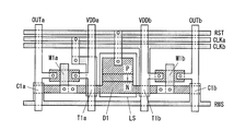
- FIG. 7 is a layout diagram of the first pixel circuit 10a.
- a light shielding film LS As shown in FIG. 7, in the first pixel circuit 10a, a light shielding film LS, a semiconductor layer (shaded portion), a gate wiring layer (dot pattern portion), and a source wiring layer (white coating portion) are sequentially formed on a glass substrate. It is constituted by. Contacts (indicated by white circles) are provided at locations where the semiconductor layer and the source wiring layer are connected, and where the gate wiring layer and the source wiring layer are connected.
- the transistors T1a and M1a are formed by arranging a semiconductor layer and a gate wiring layer so as to cross each other.
- the photodiode D1a is formed by arranging the P layer, I layer, and N semiconductor layers side by side.
- the capacitor C1a is formed by arranging the semiconductor layer and the gate wiring layer so as to overlap each other.
- the light shielding film LS is made of metal, and prevents light entering from the back side of the substrate from entering the photodiode D1a.
- the second pixel circuit 10b is laid out in the same form as the first pixel circuit 10a.
- the first and second pixel circuits 10a and 10b may be laid out in a form other than the above.
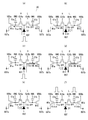
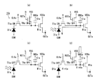
- FIG. 8 is a diagram showing the operation of the first pixel circuit 10a when driven by the signal shown in FIG. As shown in FIG. 8, the first pixel circuit 10a performs (a) reset, (b) accumulation, (c) holding, and (d) reading in one frame period.
- FIG. 9 is a signal waveform diagram of the first pixel circuit 10a and the second pixel circuit 10b when driven by the signal shown in FIG.
- BL represents the luminance of the infrared LED 3b
- Vinta represents the potential of the storage node of the first pixel circuit 10a (gate potential of the transistor M1a)
- Vintb represents the potential of the storage node of the second pixel circuit 10b (transistor M1b).
- the reset period is from time t1 to time t2
- the storage period is from time t2 to time t3
- the holding period is from time t3 to time t7
- the readout period is from time t7 to time t8.
- the time t4 to time t5 is the reset period
- the time t5 to time t6 is the accumulation period
- the time t6 to time t7 is the holding period
- the time t7 to time t8 is the reading period.
- the clock signal CLKa is at a high level
- the readout signal RWSa is at a low level
- the reset signal RSTa is at a reset high level.
- the transistor T1a is turned on. Therefore, a current (forward current of the photodiode D1a) flows from the reset line RSTa to the storage node via the photodiode D1a and the transistor T1a (FIG. 8A), and the potential Vanta is reset to a predetermined level.
- the clock signal CLKa is at a high level, and the reset signal RSTa and the readout signal RWSa are at a low level.
- the transistor T1a is turned on.
- a current photocurrent of the photodiode D1a
- the potential Vanta drops according to the amount of light incident during the period in which the clock signal CLKa is at the high level (the lighting period of the infrared LED 3b).
- the clock signal CLKa, the reset signal RSTa, and the readout signal RWSa are at a low level.
- the transistor T1a is turned off. Even if light is incident on the photodiode D1a at this time, the transistor T1a is off and the gate of the photodiode D1a and the transistor M1 is electrically cut off, so that the potential Vanta does not change (FIG. 8). (C)).
- the clock signal CLKa and the reset signal RSTa are at a low level, and the readout signal RWSa is at a readout high level.
- the transistor T1a is turned off.
- the potential Vanta increases by (Cqa / Cpa) times the increase amount of the potential of the readout signal RWSa (where Cpa is the overall capacitance value of the first pixel circuit 10a and Cqa is the capacitance value of the capacitor C1a).
- the transistor M1a forms a source follower amplifier circuit using a transistor (not shown) included in the source driver circuit 6 as a load, and drives the output line OUTa according to the potential Vanta (FIG. 8D).
- the second pixel circuit 10b operates in the same manner as the first pixel circuit 10a.
- the potential Vintb is reset to a predetermined level during the reset period, falls during the accumulation period according to the amount of light incident during the period during which the clock signal CLKb is at the high level (the extinguishing period of the infrared LED 3b), and does not change during the holding period.
- the potential Vintb increases by (Cqb / Cpb) times the amount of increase in the potential of the readout signal RWSb (where Cpb is the overall capacitance value of the second pixel circuit 10b, and Cqb is the capacitance value of the capacitor C1b).
- the transistor M1b drives the output line OUTb according to the potential Vintb.
- the first pixel circuit 10a includes one photodiode D1a (photosensor), one accumulation node that accumulates charges according to the detected light amount, and an accumulation node. It includes a transistor M1a (readout transistor) having a connected control terminal, and a transistor T1a (holding switching element) provided on the path of a current flowing through the photodiode D1a and turned on / off in accordance with the clock signal CLK.
- the transistor T1a is provided between the storage node and one end of the photodiode D1a, and the other end of the photodiode D1a is connected to the reset line RSTa.
- the transistor T1a is turned on in the detection period when the backlight is lit in accordance with the clock signal CLKa.
- the second pixel circuit 10b has the same configuration as the first pixel circuit 10a, and the transistor T1b included in the second pixel circuit 10b is turned on in the detection period when the backlight is turned off.
- the transistor T1a that is turned on in the detection period when the backlight is turned on is provided on the path of the current flowing through the photodiode D1a, and the transistor T1b that is turned on in the detection period when the backlight is turned off on the path of the current flowing through the photodiode D1b
- the first pixel circuit 10a that detects light during the detection period when the backlight is turned on, and holds the detected light amount otherwise, the light is detected during the detection period when the backlight is turned off, and otherwise
- the second pixel circuit 10b that holds the detected light amount can be configured.
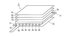
- FIG. 10 to 14 are exploded perspective views showing examples of the configuration of the backlight 3, respectively.
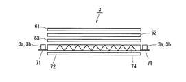
- FIG. 15 is a cross-sectional view showing a schematic configuration of the backlight 3 shown in FIG.
- two lens sheets 61 and 62 and a diffusion sheet 63 are provided on one surface of the light guide plate 64 or 74, and a reflection sheet 65 or 72 is provided on the other surface. It has been.
- a flexible printed circuit board 66 in which white LEDs 3 a are arranged one-dimensionally is provided on the side surface of the light guide plate 64.
- the infrared LEDs 3b are arranged two-dimensionally on the circuit board 67.
- the circuit board 67 is provided on the back side of the reflection sheet 65.
- the reflection sheet 65 is formed of a sheet that transmits infrared light and reflects visible light. As such a sheet, for example, a reflective sheet formed of a polyester resin can be used.
- a flexible printed circuit board 66 in which white LEDs 3 a are arranged one-dimensionally is provided on the side surface of the light guide plate 64.
- the backlight 3 shown in FIG. 11 includes another light guide plate 68 in addition to the light guide plate 64.
- the infrared LED 3 b is provided on the side surface of the light guide plate 68 in a state of being arranged one-dimensionally on the flexible substrate 69.
- a reflection sheet 70 is provided on the back side of the light guide plate 68.
- the reflection sheet 70 is formed of a sheet that reflects infrared light. According to the backlight 3 having the configuration shown in FIG.
- the backlight 3 that emits both visible light and infrared light can be configured using the backlight structure for visible light as it is.
- a flexible printed circuit board 71 in which white LEDs 3 a and infrared LEDs 3 b are mixed and arranged one-dimensionally is provided on the side surface of the light guide plate 64.
- the white LED 3a and the infrared LED 3b are alternately arranged on the flexible printed circuit board 71, for example.
- As the reflection sheet 72 a sheet that reflects both visible light and infrared light is used. In this way, by arranging the white LED 3a and the infrared LED 3b together along the side surface of the light guide plate 64, the visible light backlight structure is used almost as it is, and both visible light and infrared light are used.
- the emitted backlight 3 can be configured.
- the white LED 3a and the infrared LED 3b are enclosed together in the same resin package 14.
- a flexible printed circuit board 73 on which the resin package 14 is arranged one-dimensionally is provided on the side surface of the light guide plate 64.
- One resin package 14 may enclose one white LED 3a and one infrared LED 3b, or a plurality of white LEDs 3a and one infrared LED 3b.
- a flexible printed circuit board 71 in which white LEDs 3 a and infrared LEDs 3 b are mixed and arranged one-dimensionally is provided on one side surface of the light guide plate 74.
- a flexible printed circuit board 71 in which white LEDs 3a and infrared LEDs 3b are mixedly arranged in a one-dimensional manner is also provided on the side surface facing the one side surface.
- FIG. 15 is a cross-sectional view of the backlight 3 shown in FIG.
- the light guide plate 74 is processed so that white light and infrared light incident from one side surface and white light and infrared light incident from the opposite side surface propagate.
- white LED 3a and the infrared LED 3b along two opposing side surfaces in the light guide plate 74, these two types of LEDs share the light guide plate 74 and other backlight members. .
- emits both visible light and infrared light is realizable with a more compact structure.
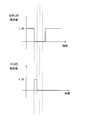
- FIG. 16 to 19 are signal waveform diagrams showing examples of drive currents CS3a and CS3b output from the backlight control circuit 13 to the backlight 3.
- FIG. 16 to 19 the waveform of the drive current CS3a for controlling the lighting / light-off timing of the white LED 3a is shown in the upper stage, and the waveform of the drive current CS3b for controlling the lighting / light-off timing of the infrared LED 3b is shown in the lower stage.
- the drive current CS3b having the current value I_3b is supplied to the infrared LED 3b (that is, the period in which the infrared LED 3b is lit), and is supplied to the white LED 3a as shown in the upper stage.
- the current value of the drive current CS3a is zero. Note that the period during which the drive current CS3b having the current value I_3b is supplied to the infrared LED 3b corresponds to the period A1 from time ta to tb shown in FIG.
- the current value of the drive current CS3a supplied to the white LED 3a is maintained at a constant value I_3a during a period other than the period during which the infrared LED 3b is lit.
- the current values I_3a and I_3b are preferably set so that the sum of the power of the white LED 3a and the power of the infrared LED 3b is always constant.
- the drive current CS3b having the current value I_3b is supplied to the infrared LED 3b (that is, the period in which the infrared LED 3b is lit), and is supplied to the white LED 3a as shown in the upper stage.
- the drive current CS3a has a current value I_3a ′ that is lower than the current value I_3a during normal lighting.
- the period during which the drive current CS3b having the current value I_3b is supplied to the infrared LED 3b corresponds to the period A1 from time ta to tb shown in FIG.
- the current value of the drive current CS3a supplied to the white LED 3a is kept at a constant value I_3a during a period other than the period when the infrared LED 3b is lit.
- the values of the current values I_3a, I_3a 'and I_3b are preferably set so that the total fluctuation between the power of the white LED 3a and the power of the infrared LED 3b does not become too large when the infrared LED 3b is turned on.
- the current value of the drive current CS3a supplied to the LED 3a becomes zero.
- the period during which the drive current CS3b having the current value I_3b is supplied to the infrared LED 3b corresponds to the period A1 from time ta to tb shown in FIG.
- the current value of the drive current CS3a supplied to the white LED 3a is maintained at zero for a while even after the period during which the infrared LED 3b is turned on.
- the white LED 3a is switched to the white LED 3a in a period corresponding to about three times the period A1.
- the current value of the supplied drive current CS3a is kept at zero.
- the current values I_3a and I_3b are preferably set so that the sum of the power of the white LED 3a and the power of the infrared LED 3b when the infrared LED 3b is lit does not vary compared to immediately before lighting.
- the current value of the drive current CS3a supplied to the white LED 3a is zero for a while after the infrared LED 3b is turned on. This current value is as shown in FIG.
- the value may be larger than zero and lower than the current value I_3a during normal lighting.
- the current value of the drive current CS3a supplied to the white LED 3a becomes zero.
- the time from when the current value of the drive current CS3a supplied to the white LED 3a becomes zero until the infrared LED 3b starts to light is the period during which the infrared LED 3b is lit (shown in FIG. 3). It is set to be substantially the same as the length of the period A1) from time ta to tb.
- the period during which the drive current CS3b having the current value I_3b is supplied to the infrared LED 3b corresponds to the period A1 from time ta to tb shown in FIG.
- the current value of the drive current CS3a supplied to the white LED 3a is maintained at zero for a while after the lighting period of the infrared LED 3b ends.
- the current value of the drive current CS3a supplied to the white LED 3a becomes zero in a period corresponding to about three times the period A1 after the lighting period of the infrared LED 3b ends. It is kept.
- the timing and length of the period during which the white LED 3a is turned off can be arbitrarily set as long as it falls within a range that does not affect the display such as the blanking period.
- the current values I_3a and I_3b are preferably set so that the sum of the power of the white LED 3a and the power of the infrared LED 3b when the infrared LED 3b is lit does not vary compared to when the white LED 3a is lit.
- the current value of the drive current CS3a supplied to the white LED 3a is set to zero for a while after the infrared LED 3b is turned on. This current value is as shown in FIG.
- the value may be larger than zero and lower than the current value I_3a during normal lighting.
- FIG. 20 is a signal waveform diagram of the drive currents CS3a and CS3b when the white LED 3a continues to be lit even during the lighting period of the infrared LED 3b as a comparative example with the examples shown in FIGS.
- the instantaneous voltage drop during the period in which the infrared LED 3b is lit in the backlight 3 can be suppressed.
- problems such as a decrease in luminance of the white LED 3a, insufficient infrared intensity of the infrared LED 3b, or malfunction of the drive circuit.
- the upper limit of the current value I_3b supplied to the infrared LED 3b can be improved, and there is an advantage that the infrared intensity of the infrared LED 3b is improved.
- the upper limit of the current value I_3b supplied to the infrared LED 3b can be improved and the infrared intensity of the infrared LED 3b is improved as in the examples shown in FIGS. is there.
- the white LED 3a is turned off also in the period A2 shown in FIG. 3, the output signal of the second sensor pixel circuit 9b that performs sensing in the period A2 is output from the white LED 3a. Only noise components are included without being affected by the emitted light. Thus, a more accurate sensor output can be obtained by subtracting the output signal of the second sensor pixel circuit 9b from the output signal of the first sensor pixel circuit 9a.
- the upper limit of the current value I_3b supplied to the infrared LED 3b can be improved, and the infrared intensity of the infrared LED 3b is improved. is there.
- the white LED 3 a is turned off during the period A ⁇ b> 2 shown in FIG. 3, more accurate sensor output can be obtained.
- the white LED 3a is turned off before the infrared LED 3b is turned on (at the start of the period A1), only the reflected light of the light emitted from the infrared LED 3b in the period A1 is detected.
- FIG. 21 is a circuit diagram showing a schematic configuration of the backlight control circuit 13 for controlling the backlight 3 by the drive current shown in FIG.
- the backlight control circuit 13 receives a voltage supply from an external power supply 18.
- the backlight control circuit 13 includes a power supply control circuit 131 and switch elements 132a and 132b. As the signals, the on / off signal, the WCNT signal, and the IR CNT signal shown in FIG. 21 are given to the backlight control circuit 13 as the control signal CSb shown in FIG.
- the on / off signal controls on / off of the power supply control circuit 131.
- the WCNT signal is supplied to the gate electrode of the switch element 132a, and controls on / off of the switch element 132a.
- the IR CNT signal is supplied to the gate electrode of the switch element 132b, and controls on / off of the switch element 132b.
- the W CNT signal and the IR CNT signal are signals having opposite polarities. Therefore, if one of the W CNT signal and the IR CNT signal is on (high level), the other is off (low level).
- the source electrode of the switch element 132a is connected to the resistor R2.
- the source electrode of the switch element 132b is connected to the resistor R3.
- the drain electrodes of the switch elements 132 a and 132 b are connected to the FB terminal of the backlight control circuit 13.
- FIG. 22 is a timing chart showing the operation of the backlight control circuit 13.
- a constant voltage Va [V] is always applied from the output terminal (V_out) of the power supply control circuit 131 to the anodes of the white LED 3a and the infrared LED 3b.
- V_out the output terminal of the power supply control circuit 131
- W CNT signal switching device 132a is turned on because it is a high level, (in this example 20 [mA]) the current value is high level of the drive current CS3a supplied to white LED3a and become. Thereby, the white LED 3a is in a lighting state (ON).
- the switch element 132b is turned off, and the current value of the drive current CS3b supplied to the infrared LED 3b is at a low level (in this example, 0 [mA]). Thereby, the infrared LED 3b is turned off (OFF).
- the IR CNT signal is switched from the low level to the high level, and the W CNT signal is switched from the high level to the low level.
- the current value of the drive current CS3a supplied to the switch white LED 3a becomes a low level (0 [mA] in this example)
- the current value of the drive current CS3b supplied to the infrared LED 3b becomes a high level (100 in this example). [MA]).
- the white LED 3a is turned off (OFF), and the infrared LED 3b is turned on (ON).
- the period from time t2 to t3 corresponds to the period A1 from time ta to tb shown in FIG.
- the IR CNT signal is switched from the high level to the low level, and the W CNT signal is switched from the low level to the high level.
- the current value of the drive current CS3a supplied to the switch white LED 3a becomes a high level
- the current value of the drive current CS3b supplied to the infrared LED 3b becomes a low level.
- the white LED 3a is turned on (ON), and the infrared LED 3b is turned off (OFF).
- the backlight control circuit 13 is configured to be able to control the turning on / off of both the white LED 3a and the infrared LED 3b by a single power supply control circuit 131. Therefore, for example, as shown in FIGS. 23A and 23B as a comparative example, the circuit configuration can be simplified as compared with the case where the lighting control circuit for the white LED 3a and the lighting control circuit for the infrared LED 3b are provided separately.
- the circuit examples shown in FIGS. 23A and 23B are lighting control circuits for temporarily turning on the infrared LEDs 3b while always turning on the white LEDs 3a, as shown in FIG. 20 as a comparative example.
- the backlight control circuit 13 of the present embodiment when the infrared LED 3b is lit in the period A1, the current value of the drive current CS3b supplied to the white LED 3b is suppressed or completely zero. To do. Thereby, there is an advantage that an instantaneous voltage drop when the infrared LED 3b is turned on can be suppressed, and a display defect and a touch panel malfunction can be prevented.
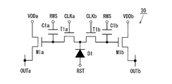
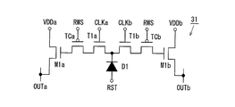
- FIG. 24 is a circuit diagram of a pixel circuit according to the second embodiment of the present invention.
- a pixel circuit 30 shown in FIG. 24 includes transistors T1a, T1b, M1a, M1b, a photodiode D1, and capacitors C1a, C1b.
- the transistors T1a, T1b, M1a, and M1b are N-type TFTs.
- the left half corresponds to the first pixel circuit
- the right half corresponds to the second pixel circuit.
- the pixel circuit 30 is connected to clock lines CLKa and CLKb, a reset line RST, a readout line RWS, power supply lines VDDa and VDDb, and output lines OUTa and OUTb.
- the anode of the photodiode D1 is connected to the reset line RST, and the cathode is connected to the sources of the transistors T1a and T1b.
- the gate of the transistor T1a is connected to the clock line CLKa, and the drain is connected to the gate of the transistor M1a.
- the drain of the transistor M1a is connected to the power supply line VDDa, and the source is connected to the output line OUTa.
- the capacitor C1a is provided between the gate of the transistor M1a and the read line RWS.
- the gate of the transistor T1b is connected to the clock line CLKb, and the drain is connected to the gate of the transistor M1b.
- the drain of the transistor M1b is connected to the power supply line VDDb, and the source is connected to the output line OUTb.
- the capacitor C1b is provided between the gate of the transistor M1b and the read line RWS.
- a node connected to the gate of the transistor M1a is a first storage node
- a node connected to the gate of the transistor M1b is a second storage node
- the transistors M1a and M1b function as readout transistors.
- FIG. 25 is a layout diagram of the pixel circuit 30. The description of FIG. 25 is the same as that of the first embodiment.
- FIG. 26 is a diagram illustrating the operation of the pixel circuit 30.
- the pixel circuit 30 includes (a) reset when the infrared LED 3b is turned on, (b) accumulation when the infrared LED 3b is turned on, (c) reset when the infrared LED 3b is turned off, (d) accumulation when the infrared LED 3b is turned off, e) Hold and (f) read.
- FIG. 27 is a signal waveform diagram of the pixel circuit 30.
- Vanta represents the potential of the first accumulation node (gate potential of the transistor M1a)
- Vintb represents the potential of the second accumulation node (gate potential of the transistor M1b).
- time t1 to time t2 is the reset period when the infrared LED 3b is lit
- time t2 to time t3 is the accumulation period when the infrared LED 3b is lit
- time t4 to time t5 is the reset period when the infrared LED 3b is lit
- time t5 to time t6 is an accumulation period when the infrared LED 3b is extinguished
- time t3 to time t4 and time t6 to time t7 are holding periods
- time t7 to time t8 are reading periods.
- the clock signal CLKa is at a high level
- the clock signal CLKb and the readout signal RWS are at a low level
- the reset signal RST is at a high level for reset.
- the transistor T1a is turned on and the transistor T1b is turned off. Therefore, a current (forward current of the photodiode D1) flows from the reset line RST to the first accumulation node via the photodiode D1 and the transistor T1a (FIG. 26A), and the potential Vanta is reset to a predetermined level. .
- the clock signal CLKa is at a high level
- the clock signal CLKb, the reset signal RST, and the readout signal RWS are at a low level.
- the transistor T1a is turned off and the transistor T1a is turned off.
- a current photocurrent of the photodiode D1 flows from the first storage node to the reset line RST via the transistor T1a and the photodiode D1, and the charge is transferred from the first storage node. It is pulled out (FIG. 26 (b)). Therefore, the potential Vanta falls according to the amount of light incident during this period (lighting time of the infrared LED 3b). Note that the potential Vintb does not change during this period.
- the clock signal CLKb is at a high level
- the clock signal CLKa and the readout signal RWS are at a low level
- the reset signal RST is at a high level for reset.
- the transistor T1a is turned off and the transistor T1b is turned on. Therefore, a current (forward current of the photodiode D1) flows from the reset line RST to the second accumulation node via the photodiode D1 and the transistor T1b (FIG. 26C), and the potential Vintb is reset to a predetermined level. .
- the clock signal CLKb is at a high level
- the clock signal CLKa, the reset signal RST, and the readout signal RWS are at a low level.
- the transistor T1a is turned off and the transistor T1b is turned on.
- a current photocurrent of the photodiode D1 flows from the second storage node to the reset line RST via the transistor T1b and the photodiode D1, and the charge is transferred from the second storage node. It is pulled out (FIG. 26 (d)). Therefore, the potential Vintb falls according to the amount of light incident during this period (the turn-off time of the infrared LED 3b). Note that the potential Vanta does not change during this period.
- the clock signals CLKa and CLKb, the reset signal RST, and the read signal RWS are at a low level.
- the transistors T1a and T1b are turned off. Even if light is incident on the photodiode D1 at this time, the transistors T1a and T1b are turned off, and the gates of the photodiode D1 and the transistors M1a and M1b are electrically disconnected. Therefore, the potentials Vinta and Vintb Does not change (FIG. 26E).
- the clock signals CLKa and CLKb and the reset signal RST are at a low level, and the read signal RWS is at a high level for reading.
- the transistors T1a and T1b are turned off.
- the potentials Vinta and Vintb increase by the increase in the potential of the read signal RWS, a current Ia corresponding to the potential Vinta flows between the drain and source of the transistor M1a, and the potential between the drain and source of the transistor M1b.
- An amount of current Ib corresponding to Vintb flows (FIG. 26 (f)).
- the current Ia is input to the source driver circuit 6 via the output line OUTa
- the current Ib is input to the source driver circuit 6 via the output line OUTb.
- the pixel circuit 30 has a configuration in which one photodiode D1 (photosensor) is shared between the first and second pixel circuits 10a and 10b according to the first embodiment.
- the cathode of the shared photodiode D1 is connected to the source of the transistor T1a included in the portion corresponding to the first pixel circuit and the source of the transistor T1b included in the portion corresponding to the second pixel circuit.
- the pixel circuit 30 can detect the light amount when the infrared LED 3b is turned on and the light amount when the infrared LED 3b is turned off, as in the first and second pixel circuits 10a and 10b according to the first embodiment. Thereby, the effect similar to 1st Embodiment is acquired. Further, by sharing one photodiode D1 between the two types of pixel circuits, the influence of variation in sensitivity characteristics of the photodiode is canceled, and the difference between the light amount when the infrared LED 3b is turned on and the light amount when the infrared LED 3b is turned off. Can be obtained accurately. In addition, the number of photodiodes can be reduced, the aperture ratio can be increased, and the sensitivity of the sensor pixel circuit can be increased.
- the backlight control circuit 13 lights the infrared LED 3b in the period A1
- the current value of the drive current CS3b supplied to the white LED 3b is suppressed or completely zero.
- the display device differs from the first embodiment in the internal configuration of the first sensor pixel circuit 9a and the second sensor pixel circuit 9b.
- FIGS. 28A to 28E show specific examples of circuit configurations used as the first sensor pixel circuit 9a and the second sensor pixel circuit 9b according to this embodiment, respectively.
- the first pixel circuits 11a to 17a shown in FIGS. 28A to 28E are obtained by making the following modifications to the first pixel circuit 10a according to the first embodiment.
- the second pixel circuits 11b to 17b are obtained by performing the same modification on the second pixel circuit 10b according to the first embodiment.
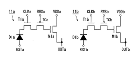
- the first pixel circuit 11a shown in FIG. 28A is obtained by replacing the capacitor C1a included in the first pixel circuit 10a with a transistor TCa that is a P-type TFT.
- the drain of the transistor TCa is connected to the drain of the transistor T1a
- the source is connected to the gate of the transistor M1a
- the gate is connected to the readout line RWSa.
- the transistor TCa connected in this way changes the potential of the storage node more than the original pixel circuit when a high level for reading is applied to the reading line RWSa.
- the difference between the potential of the storage node when the strong light is incident and the potential of the storage node when the weak light is incident can be amplified to improve the sensitivity of the pixel circuit 11a.
- a pixel circuit 31 illustrated in FIG. 33A is obtained.
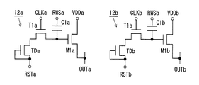
- the first pixel circuit 12a shown in FIG. 28B is obtained by replacing the photodiode D1 included in the first pixel circuit 10a with a phototransistor TDa. Thereby, all the transistors included in the first pixel circuit 12a are N-type. Therefore, the first pixel circuit 12a can be manufactured using a single channel process that can manufacture only N-type transistors. When the same modification is performed on the second embodiment, the pixel circuit 32 shown in FIG. 33B is obtained.
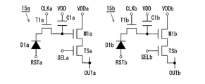
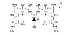
- the first pixel circuit 15a shown in FIG. 28C is obtained by adding a transistor TSa to the first pixel circuit 10a.
- the transistor TSa is an N-type TFT and functions as a selection switching element.
- the source of the transistor M1a is connected to the drain of the transistor TSa.
- the source of the transistor TSa is connected to the output line OUTa, and the gate is connected to the selection line SELa.
- the selection signal SELa is at a high level when reading from the first pixel circuit 15a. Thereby, variations of the pixel circuit can be obtained.
- a pixel circuit 35 shown in FIG. 33C is obtained.
- FIG. 29 is a diagram illustrating the operation of the first pixel circuit 15a in the sensor drive mode.
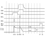
- FIG. 30 is a signal waveform diagram of the first pixel circuit 15a.
- the selection signal SELa becomes low level, the transistor TSa is turned off, and the first pixel circuit 15a operates in the same manner as the first pixel circuit 10a (FIGS. 29A to 29C).
- the selection signal SELa becomes high level and the transistor TSa is turned on.
- an amount of current Ia corresponding to the potential Vanta flows between the drain and source of the transistor M1a (FIG. 29D).
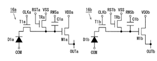
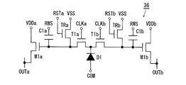
- the first pixel circuit 16a shown in FIG. 28D is obtained by adding a transistor TRa to the first pixel circuit 10a.
- the transistor TRa is an N-type TFT and functions as a reset switching element.
- the low-level potential VSS is applied to the source of the transistor TRa, the drain is connected to the gate of the transistor M1a, and the gate is connected to the reset line RSTa.
- the low level potential COM is applied to the anode of the photodiode D1a.
- the pixel circuit 36 shown in FIG. 33D is obtained.
- FIG. 31 is a diagram showing the operation of the first pixel circuit 16a in the sensor drive mode.
- the reset signal RSTa becomes high level, the transistor TRa is turned on, and the potential of the storage node (the gate potential of the transistor M1a) is reset to the low level potential VSS (FIG. 31A).
- the reset signal RSTa is at a low level, and the transistor TRb is turned off (FIGS. 31B to 31D).
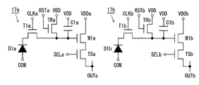
- the first pixel circuit 17a shown in FIG. 28E is obtained by adding the transistors TSa and TRa to the first pixel circuit 10a.
- the connection form of the transistors TSa and TRa is the same as that of the first pixel circuits 15a and 16a. Thereby, variations of the pixel circuit can be obtained.
- a pixel circuit 37 shown in FIG. 33E is obtained.
- FIG. 32 is a diagram illustrating the operation of the first pixel circuit 17a in the sensor drive mode.
- the reset signal RSTa becomes high level
- the transistor TRa is turned on
- the potential of the storage node (gate potential of the transistor M1a) is reset to the high level potential VDD (FIG. 32 (a)).
- the selection signal SELa becomes high level and the transistor TSa is turned on.
- an amount of current Ia corresponding to the potential Vanta flows between the drain and source of the transistor M1a (FIG. 32 (d)).
- the reset signal RSTa and the selection signal SELa are at a low level (FIGS. 32B and 32C).
- the first sensor pixel circuit that detects light during the detection period when the infrared LED 3b is turned on and holds the detected light amount otherwise, and the infrared LED 3b is turned off.
- a second sensor pixel circuit that detects light during the detection period and holds the detected light quantity otherwise, and if the difference between the two kinds of light quantity is obtained outside the sensor pixel circuit, the light quantity when the infrared LED 3b is lit The difference in the amount of light when the backlight is turned off can be detected. Thereby, an input function independent of the light environment can be provided.
- the backlight control circuit 13 lights the infrared LED 3b in the period A1
- the current value of the drive current CS3b supplied to the white LED 3b is suppressed or completely zero.
- the sensor pixel circuit is divided into the first sensor pixel circuit 9a and the second sensor pixel circuit 9b, and light is detected by the first sensor pixel circuit 9a in the period A1 illustrated in FIG. In the period B1, light is detected by the second sensor pixel circuit 9b, and a difference between the detected light amounts is obtained.
- the present invention is industrially applicable as a display device having an optical sensor function using invisible light.
Landscapes
- Engineering & Computer Science (AREA)
- Theoretical Computer Science (AREA)
- Physics & Mathematics (AREA)
- General Physics & Mathematics (AREA)
- General Engineering & Computer Science (AREA)
- Computer Hardware Design (AREA)
- Human Computer Interaction (AREA)
- Chemical & Material Sciences (AREA)
- Crystallography & Structural Chemistry (AREA)
- Control Of Indicators Other Than Cathode Ray Tubes (AREA)
- Liquid Crystal (AREA)
Abstract
可視光光源と非可視光光源とを併せ持ち、非可視光光源を点灯した際の電圧降下が抑制された光センサ付き表示装置を提供する。表示装置は、アクティブマトリクス基板と、前記アクティブマトリクス基板の画素領域(4)に設けられた光センサ(9)と、画素領域(4)に画像を表示させるための白色LED(3a)と、前記光センサで反射光を検出するための赤外線LED(3b)と、白色LED(3a)および赤外線LED(3b)の点灯および消灯を制御する光源制御回路(13)とを備える。光源制御回路(13)は、赤外線LED(3b)が点灯している期間に、白色LED(3a)へ供給する駆動電流を、赤外線LED(3b)の消灯時に白色LED(3a)へ供給する駆動電流よりも減少させるよう構成されている。
Description
本発明は、フォトダイオード等の光検出素子を有する光センサ付きの表示装置に関し、特に、検出光用の光源として表示用光源とは異なる光源を備えた表示装置に関する。
従来、例えばフォトダイオード等の光検出素子を画素内に備えたことにより、外光の明るさを検出したり、ディスプレイに近接した物体の画像を取り込んだりすることが可能な、光センサ付き表示装置が提案されている。このような光センサ付き表示装置は、双方向通信用表示装置や、タッチパネル機能付き表示装置としての利用が想定されている。
このような光センサ付き表示装置として、可視光線と非可視光線をそれぞれ出射する異なる光源を組み合わせたバックライトを用い、これらの光源を異なるタイミングで点灯させることにより、画像表示と独立して物体の位置検出を行う構成が、例えば特開2005-275644号公報に開示されている。
前述のように、可視光線用の光源と非可視光線用の光源とを組み合わせたバックライトを用いる構成においては、光センサが光を検出するタイミングに合わせて、非可視光線用の光源を駆動することとなる。この場合、非可視光線用の光源を点灯した時に、バックライトにおいて瞬間的に電圧降下が生じることがある、という課題があった。
本発明は、上記の課題を鑑み、可視光光源と非可視光光源とを併せ持つ光センサ付き表示装置において、非可視光光源を点灯した際の電圧降下を抑制することを目的とする。
ここに開示する表示装置は、アクティブマトリクス基板と、前記アクティブマトリクス基板の画素領域に設けられた光センサと、前記画素領域に画像を表示させるための可視光光源と、前記光センサで反射光を検出するための非可視光光源と、前記可視光光源および前記非可視光光源の点灯および消灯を制御する光源制御回路とを備え、前記光源制御回路が、前記非可視光光源が点灯している期間に、前記可視光光源へ供給する駆動電流を、前記非可視光光源の消灯時に当該可視光光源へ供給する駆動電流よりも減少させるよう構成されている。
上述の構成によれば、可視光光源と非可視光光源とを併せ持ち、非可視光光源を点灯した際の電圧降下が抑制された光センサ付き表示装置を提供することができる。
本発明の一実施形態にかかる表示装置は、
アクティブマトリクス基板と、
前記アクティブマトリクス基板の画素領域に設けられた光センサと、
前記画素領域に画像を表示させるための可視光光源と、
前記光センサで反射光を検出するための非可視光光源と、
前記可視光光源および前記非可視光光源の点灯および消灯を制御する光源制御回路とを備え、
前記光源制御回路が、前記非可視光光源が点灯している期間に、前記可視光光源へ供給する駆動電流を、前記非可視光光源の消灯時に当該可視光光源へ供給する駆動電流よりも減少させるよう構成されている(第1の構成)。
アクティブマトリクス基板と、
前記アクティブマトリクス基板の画素領域に設けられた光センサと、
前記画素領域に画像を表示させるための可視光光源と、
前記光センサで反射光を検出するための非可視光光源と、
前記可視光光源および前記非可視光光源の点灯および消灯を制御する光源制御回路とを備え、
前記光源制御回路が、前記非可視光光源が点灯している期間に、前記可視光光源へ供給する駆動電流を、前記非可視光光源の消灯時に当該可視光光源へ供給する駆動電流よりも減少させるよう構成されている(第1の構成)。
前記第1の構成において、
前記非可視光光源の点灯時における当該非可視光光源の電力と前記可視光光源の電力との和が、前記非可視光光源の消灯時における当該非可視光光源の電力と前記可視光光源の電力との和に等しい構成とすることができる(第2の構成)。
前記非可視光光源の点灯時における当該非可視光光源の電力と前記可視光光源の電力との和が、前記非可視光光源の消灯時における当該非可視光光源の電力と前記可視光光源の電力との和に等しい構成とすることができる(第2の構成)。
前記第1の構成において、
前記可視光光源へ供給する駆動電流を減少させる期間の長さが、前記非可視光光源の点灯期間よりも長い構成とすることもできる(第3の構成)
前記可視光光源へ供給する駆動電流を減少させる期間の長さが、前記非可視光光源の点灯期間よりも長い構成とすることもできる(第3の構成)
前記第1の構成において、
前記光源制御回路が、前記可視光光源へ供給する駆動電流を減少させる期間を、前記非可視光光源の点灯よりも前に開始する構成としても良い(第4の構成)。
前記光源制御回路が、前記可視光光源へ供給する駆動電流を減少させる期間を、前記非可視光光源の点灯よりも前に開始する構成としても良い(第4の構成)。
前記第1~第4の構成において、
前記光源制御回路が、
前記可視光光源の第1の端子と、前記非可視光光源の第1の端子とに接続され、当該可視光光源および非可視光光源へ定電圧を供給する電源制御回路と、
前記可視光光源の第2の端子と抵抗との間に接続された第1のスイッチング素子と、
前記非可視光光源の第2の端子と抵抗との間に接続された第2のスイッチング素子とを備えた構成としても良い(第5の構成)。
前記光源制御回路が、
前記可視光光源の第1の端子と、前記非可視光光源の第1の端子とに接続され、当該可視光光源および非可視光光源へ定電圧を供給する電源制御回路と、
前記可視光光源の第2の端子と抵抗との間に接続された第1のスイッチング素子と、
前記非可視光光源の第2の端子と抵抗との間に接続された第2のスイッチング素子とを備えた構成としても良い(第5の構成)。
前記第1~第5の構成において、
前記可視光光源が白色LEDである構成としても良い(第6の構成)。
前記可視光光源が白色LEDである構成としても良い(第6の構成)。
前記第1~第6の構成において、
前記非可視光光源が赤外線LEDである構成としても良い(第7の構成)。
前記非可視光光源が赤外線LEDである構成としても良い(第7の構成)。
前記第1~第7の構成において、
前記光センサへ、センサ駆動信号を供給するセンサ駆動回路と、
前記センサ駆動信号に従って前記光センサから読み出された信号を増幅し、光センサ信号として出力するアンプ回路と、
前記アンプ回路から出力された光センサ信号を処理する信号処理回路とをさらに備え、
前記光センサには、
前記センサ駆動信号に従い、前記非可視光光源点灯時の蓄積期間で受光量に応じた電荷を蓄積し、読み出し期間が到来すると蓄積電荷に応じたセンサ信号を出力する第1センサ画素回路と、
前記センサ駆動信号に従い、前記非可視光光源消灯時の蓄積期間で受光量に応じた電荷を蓄積し、読み出し期間が到来すると蓄積電荷に応じたセンサ信号を出力する第2センサ画素回路とが含まれ、
前記信号処理回路が、前記第1センサ画素回路から出力されたセンサ信号と、前記第2センサ画素回路から出力されたセンサ信号との差分を求める構成としても良い(第8の構成)。
前記光センサへ、センサ駆動信号を供給するセンサ駆動回路と、
前記センサ駆動信号に従って前記光センサから読み出された信号を増幅し、光センサ信号として出力するアンプ回路と、
前記アンプ回路から出力された光センサ信号を処理する信号処理回路とをさらに備え、
前記光センサには、
前記センサ駆動信号に従い、前記非可視光光源点灯時の蓄積期間で受光量に応じた電荷を蓄積し、読み出し期間が到来すると蓄積電荷に応じたセンサ信号を出力する第1センサ画素回路と、
前記センサ駆動信号に従い、前記非可視光光源消灯時の蓄積期間で受光量に応じた電荷を蓄積し、読み出し期間が到来すると蓄積電荷に応じたセンサ信号を出力する第2センサ画素回路とが含まれ、
前記信号処理回路が、前記第1センサ画素回路から出力されたセンサ信号と、前記第2センサ画素回路から出力されたセンサ信号との差分を求める構成としても良い(第8の構成)。
前記第1~第8の構成において、
前記第1および第2センサ画素回路のそれぞれは、
1個の受光素子と、
検知した光量に応じた電荷を蓄積する1個の蓄積ノードと、
前記蓄積ノードに電気的に接続可能な制御端子を有する読み出しトランジスタと、
前記受光素子を流れる電流の経路上に設けられ、前記制御信号に従いオン/オフする保持用スイッチング素子とを含む構成としても良い(第9の構成)。
前記第1および第2センサ画素回路のそれぞれは、
1個の受光素子と、
検知した光量に応じた電荷を蓄積する1個の蓄積ノードと、
前記蓄積ノードに電気的に接続可能な制御端子を有する読み出しトランジスタと、
前記受光素子を流れる電流の経路上に設けられ、前記制御信号に従いオン/オフする保持用スイッチング素子とを含む構成としても良い(第9の構成)。
前記第9の構成において、
前記第1および第2センサ画素回路のそれぞれにおいて、
前記保持用スイッチング素子は、前記蓄積ノードと前記受光素子の一端との間に設けられ、
前記受光素子の他端はリセット線に接続されている構成としても良い(第10の構成)。
前記第1および第2センサ画素回路のそれぞれにおいて、
前記保持用スイッチング素子は、前記蓄積ノードと前記受光素子の一端との間に設けられ、
前記受光素子の他端はリセット線に接続されている構成としても良い(第10の構成)。
前記第1~第8の構成において、
前記第1および第2センサ画素回路は、1個の受光素子を共有し、
前記受光素子の一端は前記第1および第2センサ画素回路にそれぞれ含まれる保持用スイッチング素子の一端に接続され、他端は前記リセット線に接続されている構成としても良い(第11の構成)。
前記第1および第2センサ画素回路は、1個の受光素子を共有し、
前記受光素子の一端は前記第1および第2センサ画素回路にそれぞれ含まれる保持用スイッチング素子の一端に接続され、他端は前記リセット線に接続されている構成としても良い(第11の構成)。
前記第1~第11の構成において、
前記アクティブマトリクス基板に対向する対向基板と、
前記アクティブマトリクス基板と対向基板との間に挟持された液晶とをさらに備えた構成としても良い(第12の構成)。
前記アクティブマトリクス基板に対向する対向基板と、
前記アクティブマトリクス基板と対向基板との間に挟持された液晶とをさらに備えた構成としても良い(第12の構成)。
[実施の形態]
以下、本発明のより具体的な実施形態について、図面を参照しながら説明する。なお、以下の実施形態は、本発明にかかる表示装置を液晶表示装置として実施する場合の構成例を示したものであるが、本発明にかかる表示装置は液晶表示装置に限定されず、アクティブマトリクス基板を用いる任意の表示装置に適用可能である。なお、本発明にかかる表示装置は、光センサを有することにより、画面に近接する物体を検知して入力操作を行うタッチパネル付き表示装置や、表示機能と撮像機能とを具備した双方向通信用表示装置等としての利用が想定される。
以下、本発明のより具体的な実施形態について、図面を参照しながら説明する。なお、以下の実施形態は、本発明にかかる表示装置を液晶表示装置として実施する場合の構成例を示したものであるが、本発明にかかる表示装置は液晶表示装置に限定されず、アクティブマトリクス基板を用いる任意の表示装置に適用可能である。なお、本発明にかかる表示装置は、光センサを有することにより、画面に近接する物体を検知して入力操作を行うタッチパネル付き表示装置や、表示機能と撮像機能とを具備した双方向通信用表示装置等としての利用が想定される。
また、以下で参照する各図は、説明の便宜上、本発明の実施形態の構成部材のうち、本発明を説明するために必要な主要部材のみを簡略化して示したものである。従って、本発明にかかる表示装置は、本明細書が参照する各図に示されていない任意の構成部材を備え得る。また、各図中の部材の寸法は、実際の構成部材の寸法および各部材の寸法比率等を忠実に表したものではない。
[第1の実施形態]
図1は、本発明の第1の実施形態に係る表示装置の構成を示すブロック図である。図1に示す表示装置は、表示制御回路1、表示パネル2、バックライト3、および、バックライト制御回路13(光源制御回路)を備えている。表示パネル2は、画素領域4、ゲートドライバ回路5、ソースドライバ回路6(アンプ回路)、および、センサロウドライバ回路7(センサ駆動回路)を含んでいる。画素領域4は、複数の表示画素回路8と複数のセンサ画素回路9(光センサ)を含んでいる。この表示装置は、表示パネル2に画像を表示する機能と、表示パネル2に入射した光を検知する機能とを有する。以下、xを2以上の整数、yを3の倍数、mおよびnを偶数とし、表示装置のフレームレートを60フレーム/秒とする。
図1は、本発明の第1の実施形態に係る表示装置の構成を示すブロック図である。図1に示す表示装置は、表示制御回路1、表示パネル2、バックライト3、および、バックライト制御回路13(光源制御回路)を備えている。表示パネル2は、画素領域4、ゲートドライバ回路5、ソースドライバ回路6(アンプ回路)、および、センサロウドライバ回路7(センサ駆動回路)を含んでいる。画素領域4は、複数の表示画素回路8と複数のセンサ画素回路9(光センサ)を含んでいる。この表示装置は、表示パネル2に画像を表示する機能と、表示パネル2に入射した光を検知する機能とを有する。以下、xを2以上の整数、yを3の倍数、mおよびnを偶数とし、表示装置のフレームレートを60フレーム/秒とする。
図1に示す表示装置には外部から、映像信号Vinとタイミング制御信号Cinが供給される。表示制御回路1は、これらの信号に基づき、表示パネル2に対して映像信号VSと制御信号CSg、CSs、CSrを出力し、バックライト制御回路13に対して制御信号CSbを出力する。映像信号VSは、映像信号Vinと同じでもよく、映像信号Vinに信号処理を施した信号でもよい。
バックライト3は、表示パネル2の背面側に設けられ、表示パネル2の背面に光を照射する。バックライト3は、可視光光源としての白色LED3aと、非可視光光源としての赤外線LED(図1においてはIR-LEDと表記)3bとを含む。可視光光源(ここでは白色LED3a)は、画素領域4に画像を表示するために用いられる光源である。非可視光光源(ここでは赤外線LED3b)は、可視光以外の波長域の光を出射する光源である。非可視光光源からの出射光が、表示パネル2の表面に触れている指やタッチペン等で反射されて、センサ画素回路9へ入射することにより、タッチ位置を検出することができる。
なお、ここでは、可視光光源として白色LED3aを用い、非可視光光源として赤外線LED3bを用いるが、それぞれ他の光源を用いることも可能である。例えば、これらの光源として、LED以外の光源を用いることができる。なお、可視光光源が出射する光に、可視光以外の波長域の光が含まれていても構わない。非可視光光源からの出射光については、可視領域の波長成分が含まれていないことが好ましいが、可視領域の波長成分がゼロである必要はない。
バックライト制御回路13は、白色LED3aに対して、その点灯/消灯を制御する駆動電流CS3aを供給する。バックライト制御回路13は、赤外線LED3bに対して、その点灯/消灯を制御する駆動電流CS3bを供給する。白色LED3aおよび赤外線LED3bの点灯/消灯タイミングについては、後に詳しく説明する。
表示パネル2の画素領域4には、(x×y)個の表示画素回路8、(n×m/2)個のセンサ画素回路9が、それぞれ2次元状に配置される。より詳細には、画素領域4には、x本のゲート線GL1~GLxとy本のソース線SL1~SLyが設けられる。ゲート線GL1~GLxは互いに平行に配置され、ソース線SL1~SLyはゲート線GL1~GLxと直交するように互いに平行に配置される。(x×y)個の表示画素回路8は、ゲート線GL1~GLxとソース線SL1~SLyの交点近傍に配置される。各表示画素回路8は、1本のゲート線GLと1本のソース線SLに接続される。表示画素回路8は、赤色表示用、緑色表示用および青色表示用に分類される。これら3種類の表示画素回路8は、ゲート線GL1~GLxの伸延方向に並べて配置され、1個のカラー画素を構成する。
画素領域4には、ゲート線GL1~GLxと平行に、n本のクロック線CLK1~CLKn、n本のリセット線RST1~RSTn、および、n本の読み出し線RWS1~RWSnが設けられる。また、画素領域4には、ゲート線GL1~GLxと平行に、他の信号線や電源線(図示せず)が設けられることがある。センサ画素回路9から読み出しを行うときには、ソース線SL1~SLyの中から選択されたm本が電源線VDD1~VDDmとして使用され、別のm本が出力線OUT1~OUTmとして使用される。
図2は、画素領域4におけるセンサ画素回路9の配置を示す図である。(n×m/2)個のセンサ画素回路9には、赤外線LED3bの点灯期間に入射した光を検知する第1センサ画素回路9aと、赤外線LED3bの消灯期間に入射した光を検知する第2センサ画素回路9bとが含まれる。第1センサ画素回路9aと第2センサ画素回路9bは同数である。図2では、(n×m/4)個の第1センサ画素回路9aは、奇数番目のクロック線CLK1~CLKn-1と奇数番目の出力線OUT1~OUTm-1の交点近傍に配置される。(n×m/4)個の第2センサ画素回路9bは、偶数番目のクロック線CLK2~CLKnと偶数番目の出力線OUT2~OUTmの交点近傍に配置される。このように表示パネル2は、第1センサ画素回路9aの出力信号と第2センサ画素回路9bの出力信号を伝搬する複数の出力線OUT1~OUTmを含み、第1センサ画素回路9aと第2センサ画素回路9bは種類ごとに異なる出力線に接続される。
ゲートドライバ回路5は、ゲート線GL1~GLxを駆動する。より詳細には、ゲートドライバ回路5は、制御信号CSgに基づき、ゲート線GL1~GLxの中から1本のゲート線を順に選択し、選択したゲート線にハイレベル電位を、残りのゲート線にローレベル電位を印加する。これにより、選択されたゲート線に接続されたy個の表示画素回路8が、一括して選択される。
ソースドライバ回路6は、ソース線SL1~SLyを駆動する。より詳細には、ソースドライバ回路6は、制御信号CSsに基づき、映像信号VSに応じた電位をソース線SL1~SLyに印加する。このときソースドライバ回路6は、線順次駆動を行ってもよく、点順次駆動を行ってもよい。ソース線SL1~SLyに印加された電位は、ゲートドライバ回路5によって選択されたy個の表示画素回路8に書き込まれる。このようにゲートドライバ回路5とソースドライバ回路6を用いてすべての表示画素回路8に映像信号VSに応じた電位を書き込むことにより、表示パネル2に所望の画像を表示することができる。
センサロウドライバ回路7は、クロック線CLK1~CLKn、リセット線RST1~RSTn、および、読み出し線RWS1~RWSnなどを駆動する。より詳細には、センサロウドライバ回路7は、制御信号CSrに基づき、クロック線CLK1~CLKnに対して、図4に示すタイミングで(詳細は後述)ハイレベル電位とローレベル電位を印加する。また、センサロウドライバ回路7は、制御信号CSrに基づき、リセット線RST1~RSTnの中から(n/2)本または2本のリセット線を選択し、選択したリセット線にリセット用のハイレベル電位を、残りのリセット線にローレベル電位を印加する。これにより、ハイレベル電位が印加されたリセット線に接続された(n×m/4)個またはm個のセンサ画素回路9が、一括してリセットされる。
また、センサロウドライバ回路7は、制御信号CSrに基づき、読み出し線RWS1~RWSnの中から隣接する2本の読み出し線を順に選択し、選択した読み出し線に読み出し用のハイレベル電位を、残りの読み出し線にローレベル電位を印加する。これにより、選択された2本の読み出し線に接続されたm個のセンサ画素回路9が、一括して読み出し可能状態になる。このときソースドライバ回路6は、電源線VDD1~VDDmに対してハイレベル電位を印加する。これにより、読み出し可能状態にあるm個のセンサ画素回路9から出力線OUT1~OUTmに、各センサ画素回路9で検知した光の量に応じた信号(以下、センサ信号という)が出力される。
ソースドライバ回路6は、第1センサ画素回路9aの出力信号と第2センサ画素回路9bの出力信号の差を求める差分回路(図示せず)を含んでいる。ソースドライバ回路6は、差分回路で求めた光量の差を増幅し、増幅後の信号をセンサ出力Soutとして表示パネル2の外部に出力する。センサ出力Soutは、表示パネル2の外部に設けられた信号処理回路20によって、必要に応じて適宜の処理を施される。このようにソースドライバ回路6とセンサロウドライバ回路7を用いてすべてのセンサ画素回路9からセンサ信号を読み出すことにより、表示パネル2に入射した光を検知することができる。
図3は、赤外線LED3bの点灯および消灯タイミング、並びに、センサ画素回路9に対するリセットおよび読み出しタイミングを示す図である。図3の例では、赤外線LED3bは、1フレーム期間に1回、所定時間だけ点灯し、それ以外の期間では消灯する。具体的には、赤外線LED3bは、1フレーム期間内の時刻taにおいて点灯し、時刻tbにおいて消灯する。また、時刻taにおいてすべての第1センサ画素回路9aに対するリセットが行われ、時刻tbにおいてすべての第2センサ画素回路9bに対するリセットが行われる。
第1センサ画素回路9aは、時刻taから時刻tbまでの期間A1(赤外線LED3bの点灯期間)に入射した光を検知する。第2センサ画素回路9bは、時刻tbから時刻tcまでの期間A2(赤外線LED3bの消灯期間)に入射した光を検知する。期間A1と期間A2は同じ長さである。第1センサ画素回路9aからの読み出しと第2センサ画素回路9bからの読み出しは、時刻tc以降に並列に線順次で行われる。なお、図3では、センサ画素回路9からの読み出しは、1フレーム期間内に完了しているが、次のフレーム期間で第1センサ画素回路9aに対するリセットを行うまでに完了すればよい。
なお、図3においては、センサ画素回路9からの読み出しを1フレーム期間に1回ずつ行う例を示したが、1フレーム期間に2回以上、センサ画素回路9からの読み出しを行うようにしても良い。
図4は、図3のタイミングで駆動するための表示パネル2の信号波形図である。図4に示すように、ゲート線GL1~GLxの電位は、1フレーム期間に1回ずつ順に所定時間ずつハイレベルになる。奇数番目のクロック線CLK1~CLKn-1の電位は、1フレーム期間に1回、期間A1において(より詳細には、時刻taから時刻tbの少し前まで)ハイレベルになる。偶数番目のクロック線CLK2~CLKnの電位は、1フレーム期間に1回、期間A2において(より詳細には、時刻tbから時刻tcの少し前まで)ハイレベルになる。奇数番目のリセット線RST1~RSTn-1の電位は、1フレーム期間に1回、期間A1の始めに所定時間だけハイレベルになる。偶数番目のリセット線RST2~RSTnの電位は、1フレーム期間に1回、期間A2の始めに所定時間だけハイレベルになる。読み出し線RWS1~RWSnは2本ずつ対にされ、(n/2)対の読み出し線の電位は時刻tc以降に順に所定時間ずつハイレベルになる。
図5は、センサ画素回路9の概略構成を示す図である。図5に示すように、第1センサ画素回路9aは、1個のフォトダイオードD1a(受光素子)と1個の蓄積ノードNDaを含んでいる。フォトダイオードD1aは、赤外線LED3bが点灯している間(時刻ta~tb)に入射した光の量(信号+ノイズ)に応じた電荷を蓄積ノードNDaから引き抜く。第2センサ画素回路9bは、第1センサ画素回路9aと同様に、1個のフォトダイオードD1bと1個の蓄積ノードNDbを含んでいる。フォトダイオードD1bは、赤外線LED3bが消灯している間(時刻tb~tc)に入射した光の量(ノイズ)に応じた電荷を蓄積ノードNDbから引き抜く。第1センサ画素回路9aからは、赤外線LED3bの点灯時の検知期間に入射した光の量に応じたセンサ信号が読み出される。第2センサ画素回路9bからは、赤外線LED3bの消灯時の検知期間に入射した光の量に応じたセンサ信号が読み出される。前述のように、ソースドライバ回路6に含まれる差分回路を用いて、第1センサ画素回路9aの出力信号と第2センサ画素回路9bの出力信号の差を求めることにより、バックライト点灯時の光量とバックライト消灯時の光量の差を求めることができる。
なお、画素領域4に設けるセンサ画素回路9の個数は任意でよい。ただし、第1センサ画素回路9aと第2センサ画素回路9bとを異なる出力線に接続することが好ましい。例えば、画素領域4に(n×m)個のセンサ画素回路9を設ける場合には、奇数番目の出力線OUT1~OUTm-1のそれぞれにn個の第1センサ画素回路9aを接続し、偶数番目の出力線OUT2~OUTmのそれぞれにn個の第2センサ画素回路9bを接続すればよい。この場合、センサ画素回路9からの読み出しは行ごとに行われる。あるいは、画素領域4にカラー画素と同数の(すなわち、(x×y/3)個の)センサ画素回路9を設けてもよい。あるいは、画素領域4にカラー画素よりも少ない個数の(例えば、カラー画素の数分の1~数10分の1の)センサ画素回路9を設けてもよい。
このように本発明の実施形態に係る表示装置は、画素領域4に複数のフォトダイオード(受光素子)を配置した表示装置であって、複数の表示画素回路8および複数のセンサ画素回路9を含む表示パネル2と、センサ画素回路9に対して、バックライト点灯時の検知期間とバックライト消灯時の検知期間とを示すクロック信号CLK(制御信号)を出力するセンサロウドライバ回路7(駆動回路)とを備えている。以下、この表示装置に含まれるセンサ画素回路9の詳細を説明する。以下の説明では、センサ画素回路を画素回路と略称し、信号線上の信号を識別するために信号線と同じ名称を使用する(例えば、クロック線CLKa上の信号をクロック信号CLKaという)。
第1センサ画素回路9aは、クロック線CLKa、リセット線RSTa、読み出し線RWSa、電源線VDDaおよび出力線OUTaに接続される。第2センサ画素回路9bは、クロック線CLKb、リセット線RSTb、読み出し線RWSb、電源線VDDbおよび出力線OUTbに接続される。これらの実施形態では、第2センサ画素回路9bは第1センサ画素回路9aと同じ構成を有し同様に動作するので、第2センサ画素回路9bに関する説明を適宜省略する。
図6は、第1センサ画素回路9aおよび第2センサ画素回路9bの具体的な構成の一例を示す回路図である。本実施形態において、図6に示す第1画素回路10aが、前述の第1センサ画素回路9aの一具体例であり、第2画素回路10bが、第2センサ画素回路9bの一具体例である。図6に示すように、第1画素回路10aは、トランジスタT1a(保持用スイッチング素子)、M1a、フォトダイオードD1a、および、コンデンサC1aを含んでいる。第2画素回路10bは、トランジスタT1b、M1b、フォトダイオードD1b、および、コンデンサC1bを含んでいる。トランジスタT1a、M1a、T1b、M1bは、N型TFT(Thin Film Transistor:薄膜トランジスタ)である。
第1画素回路10aでは、フォトダイオードD1aのアノードはリセット線RSTaに接続され、カソードはトランジスタT1aのソースに接続される。トランジスタT1aのゲートはクロック線CLKaに接続され、ドレインはトランジスタM1aのゲートに接続される。トランジスタM1aのドレインは電源線VDDaに接続され、ソースは出力線OUTaに接続される。コンデンサC1aは、トランジスタM1aのゲートと読み出し線RWSaの間に設けられる。第1画素回路10aでは、トランジスタM1aのゲートに接続されたノードが、検知した光量に応じた電荷を蓄積する蓄積ノードとなり、トランジスタM1aは読み出しトランジスタとして機能する。第2画素回路10bは、第1画素回路10aと同じ構成を有する。
図7は、第1画素回路10aのレイアウト図である。図7に示すように、第1画素回路10aは、ガラス基板上に遮光膜LS、半導体層(斜線部)、ゲート配線層(点模様部)およびソース配線層(白塗り部)を順に形成することにより構成される。半導体層とソース配線層を接続する箇所、および、ゲート配線層とソース配線層を接続する箇所には、コンタクト(白円で示す)が設けられる。トランジスタT1a、M1aは、半導体層とゲート配線層を交差して配置することにより形成される。フォトダイオードD1aは、P層、I層およびN層の半導体層を並べて配置することにより形成される。コンデンサC1aは、半導体層とゲート配線層を重ねて配置することにより形成される。遮光膜LSは、金属製であり、基板の裏側から入った光がフォトダイオードD1aに入射することを防止する。第2画素回路10bは、第1画素回路10aと同様の形態にレイアウトされる。なお、第1および第2画素回路10a、10bを上記以外の形態にレイアウトしてもよい。
図8は、図4に示した信号によって駆動された場合の第1画素回路10aの動作を示す図である。図8に示すように、第1画素回路10aは、1フレーム期間に(a)リセット、(b)蓄積、(c)保持、および、(d)読み出しを行う。
図9は、図4に示した信号によって駆動された場合の第1画素回路10aと第2画素回路10bの信号波形図である。図9において、BLは赤外線LED3bの輝度を表し、Vintaは第1画素回路10aの蓄積ノードの電位(トランジスタM1aのゲート電位)を表し、Vintbは第2画素回路10bの蓄積ノードの電位(トランジスタM1bのゲート電位)を表す。第1画素回路10aについては、時刻t1~時刻t2がリセット期間、時刻t2~時刻t3が蓄積期間、時刻t3~時刻t7が保持期間、時刻t7~時刻t8が読み出し期間となる。第2画素回路10bについては、時刻t4~時刻t5がリセット期間、時刻t5~時刻t6が蓄積期間、時刻t6~時刻t7が保持期間、時刻t7~時刻t8が読み出し期間となる。
第1画素回路10aのリセット期間では、クロック信号CLKaはハイレベル、読み出し信号RWSaはローレベル、リセット信号RSTaはリセット用のハイレベルになる。このとき、トランジスタT1aはオンする。したがって、リセット線RSTaからフォトダイオードD1aとトランジスタT1aを経由して蓄積ノードに電流(フォトダイオードD1aの順方向電流)が流れ(図8(a))、電位Vintaは所定レベルにリセットされる。
第1画素回路10aの蓄積期間では、クロック信号CLKaはハイレベル、リセット信号RSTaと読み出し信号RWSaはローレベルになる。このとき、トランジスタT1aはオンする。このときにフォトダイオードD1aに光が入射すると、蓄積ノードからトランジスタT1aとフォトダイオードD1aを経由してリセット線RSTaに電流(フォトダイオードD1aのフォト電流)が流れ、蓄積ノードから電荷が引き抜かれる(図8(b))。したがって、電位Vintaは、クロック信号CLKaがハイレベルである期間(赤外線LED3bの点灯期間)に入射した光の量に応じて下降する。
第1画素回路10aの保持期間では、クロック信号CLKa、リセット信号RSTaおよび読み出し信号RWSaはローレベルになる。このとき、トランジスタT1aはオフする。このときにフォトダイオードD1aに光が入射しても、トランジスタT1aはオフしており、フォトダイオードD1aとトランジスタM1のゲートの間は電気的に遮断されているので、電位Vintaは変化しない(図8(c))。
第1画素回路10aの読み出し期間では、クロック信号CLKaとリセット信号RSTaはローレベル、読み出し信号RWSaは読み出し用のハイレベルになる。このとき、トランジスタT1aはオフする。このとき電位Vintaは、読み出し信号RWSaの電位の上昇量の(Cqa/Cpa)倍(ただし、Cpaは第1画素回路10aの全体の容量値、CqaはコンデンサC1aの容量値)だけ上昇する。トランジスタM1aは、ソースドライバ回路6に含まれるトランジスタ(図示せず)を負荷としたソースフォロワ増幅回路を構成し、電位Vintaに応じて出力線OUTaを駆動する(図8(d))。
第2画素回路10bは、第1画素回路10aと同様に動作する。電位Vintbは、リセット期間において所定レベルにリセットされ、蓄積期間ではクロック信号CLKbがハイレベルである期間(赤外線LED3bの消灯期間)に入射した光の量に応じて下降し、保持期間では変化しない。読み出し期間では、電位Vintbは読み出し信号RWSbの電位の上昇量の(Cqb/Cpb)倍(ただし、Cpbは第2画素回路10bの全体の容量値、CqbはコンデンサC1bの容量値)だけ上昇し、トランジスタM1bは電位Vintbに応じて出力線OUTbを駆動する。
以上に示すように、本実施形態に係る第1画素回路10aは、1個のフォトダイオードD1a(光センサ)と、検知した光量に応じた電荷を蓄積する1個の蓄積ノードと、蓄積ノードに接続された制御端子を有するトランジスタM1a(読み出しトランジスタ)と、フォトダイオードD1aを流れる電流の経路上に設けられ、クロック信号CLKに従いオン/オフするトランジスタT1a(保持用スイッチング素子)とを含んでいる。トランジスタT1aは蓄積ノードとフォトダイオードD1aの一端との間に設けられ、フォトダイオードD1aの他端はリセット線RSTaに接続される。トランジスタT1aは、クロック信号CLKaに従い、バックライト点灯時の検知期間でオンする。第2画素回路10bは第1画素回路10aと同様の構成を有し、第2画素回路10bに含まれるトランジスタT1bはバックライト消灯時の検知期間でオンする。
このようにフォトダイオードD1aを流れる電流の経路上にバックライト点灯時の検知期間でオンするトランジスタT1aを設け、フォトダイオードD1bを流れる電流の経路上にバックライト消灯時の検知期間でオンするトランジスタT1bを設けることにより、バックライト点灯時の検知期間では光を検知し、それ以外では検知した光量を保持する第1画素回路10aと、バックライト消灯時の検知期間では光を検知し、それ以外では検知した光量を保持する第2画素回路10bとを構成することができる。
[バックライト3の構成例]
ここで、本実施形態におけるバックライト3の構成について、いくつかの具体例を示して説明する。図10~図14は、バックライト3の構成例をそれぞれ示す分解斜視図である。図15は、図14に示すバックライト3の概略構成を示す断面図である。
ここで、本実施形態におけるバックライト3の構成について、いくつかの具体例を示して説明する。図10~図14は、バックライト3の構成例をそれぞれ示す分解斜視図である。図15は、図14に示すバックライト3の概略構成を示す断面図である。
図10~図14に示すバックライト3では、導光板64または74の一方の面に2枚のレンズシート61、62および拡散シート63が設けられ、他方の面には反射シート65または72が設けられている。
図10に示すバックライト3の場合、白色LED3aを1次元状に配置したフレキシブルプリント基板66が、導光板64の側面に設けられている。赤外線LED3bは、回路基板67上に2次元状に配置されている。この回路基板67は、反射シート65の背面側に設けられている。反射シート65は、赤外光を透過し、可視光を反射するシートで形成されている。このようなシートとしては、例えばポリエステル系樹脂で形成された反射シートを用いることができる。
図11に示すバックライト3においても、白色LED3aを1次元状に配置したフレキシブルプリント基板66が、導光板64の側面に設けられている。図11に示すバックライト3は、導光板64の他に、もう1枚の導光板68を備えている。赤外線LED3bは、フレキシブル基板69上に1次元状に配置された状態で、導光板68の側面に設けられる。図11に示すバックライト3においては、導光板68の背面側に、反射シート70が設けられている。反射シート70は、赤外光を反射するシートで形成されている。図11に示す構成のバックライト3によれば、白色LED3aを光源として可視光を出射するバックライト(すなわち、レンズシート61から反射シート65まで)に、導光板68、赤外線LED3b、フレキシブル基板69、および反射シート70を追加することにより、可視光用のバックライト構造をそのまま用いて、可視光と赤外光との両方を出射するバックライト3を構成することができる。
図12に示すバックライト3においては、白色LED3aと赤外線LED3bとを混在して1次元状に配置したフレキシブルプリント基板71が、導光板64の側面に設けられている。白色LED3aと赤外線LED3bとは、フレキシブルプリント基板71上に、例えば交互に配置される。反射シート72としては、可視光と赤外光の両方を反射するシートを使用する。このように、導光板64の側面に沿って白色LED3aと赤外線LED3bとを混在して配置することにより、可視光用のバックライト構造をほぼそのまま用いて、可視光と赤外光との両方を出射するバックライト3を構成することができる。
図13に示すバックライト3においては、白色LED3aと赤外線LED3bとが、同一の樹脂パッケージ14内に一緒に封入されている。そして、この樹脂パッケージ14が1次元状に配置されたフレキシブルプリント基板73が、導光板64の側面に設けられている。このように白色LED3aと赤外線LED3bとを1つの樹脂パッケージ14内に封入することにより、狭いスペースに多数のLED発光体を配置することができる。なお、1つの樹脂パッケージ14内に白色LED3aと赤外線LED3bとを1個ずつ封入してもよく、複数個ずつ封入してもよい。
図14に示すバックライト3においては、白色LED3aと赤外線LED3bとを混在して1次元状に配置したフレキシブルプリント基板71が、導光板74の一方の側面に設けられている。導光板74において、前記一方の側面に対向する側面にも、白色LED3aと赤外線LED3bとを混在して1次元状に配置したフレキシブルプリント基板71が設けられている。
図15は、図14に示したバックライト3の断面図である。導光板74は、一方の側面から入射した白色光および赤外光と、反対側の側面から入射した白色光および赤外光とが伝搬するように加工されている。このように、導光板74において対向する2つの側面に沿って、白色LED3aと赤外線LED3bとを配置することにより、これら2種類のLEDが導光板74およびその他のバックライト部材を共有することとなる。これにより、可視光と赤外光との両方を出射するバックライト3を、よりコンパクトな構造で実現することができる。
[白色LED3aと赤外線LED3bの点灯/消灯タイミング]
ここで、本実施形態の表示装置における、白色LED3aと赤外線LED3bの点灯/消灯タイミングについて、具体例を示しながら説明する。白色LED3aと赤外線LED3bの点灯/消灯タイミングは、バックライト制御回路13からバックライト3へ供給される駆動電流CS3aおよびCS3bによって制御される。
ここで、本実施形態の表示装置における、白色LED3aと赤外線LED3bの点灯/消灯タイミングについて、具体例を示しながら説明する。白色LED3aと赤外線LED3bの点灯/消灯タイミングは、バックライト制御回路13からバックライト3へ供給される駆動電流CS3aおよびCS3bによって制御される。
図16~図19は、バックライト制御回路13からバックライト3へ出力される駆動電流CS3a,CS3bの例を示す信号波形図である。図16~図19において、白色LED3aの点灯/消灯タイミングを制御する駆動電流CS3aの波形を上段に示し、赤外線LED3bの点灯/消灯タイミングを制御する駆動電流CS3bの波形を下段に示す。
図16に示す例では、下段に示すように、電流値I_3bの駆動電流CS3bが赤外線LED3bへ供給されている期間(すなわち赤外線LED3bが点灯する期間)、上段に示すように、白色LED3aへ供給される駆動電流CS3aの電流値がゼロとなる。なお、電流値I_3bの駆動電流CS3bが赤外線LED3bへ供給されている期間は、図3に示した時刻ta~tbの期間A1に相当する。また、この例では、赤外線LED3bが点灯する期間以外の期間においては、白色LED3aへ供給される駆動電流CS3aの電流値は一定値I_3aに保たれている。なお、電流値I_3aとI_3bの値は、白色LED3aの電力と赤外線LED3bの電力との合計が常に一定となるように設定することが好ましい。
図17に示す例では、下段に示すように、電流値I_3bの駆動電流CS3bが赤外線LED3bへ供給されている期間(すなわち赤外線LED3bが点灯する期間)、上段に示すように、白色LED3aへ供給される駆動電流CS3aの電流値が、通常点灯時の電流値I_3aよりも低いI_3a’となる。なお、この例においても、電流値I_3bの駆動電流CS3bが赤外線LED3bへ供給されている期間は、図3に示した時刻ta~tbの期間A1に相当する。また、この例においても、赤外線LED3bが点灯する期間以外の期間においては、白色LED3aへ供給される駆動電流CS3aの電流値は一定値I_3aに保たれている。電流値I_3aおよびI_3a’並びにI_3bの値は、赤外線LED3bが点灯した際の、白色LED3aの電力と赤外線LED3bの電力との合計の変動が大きくなり過ぎないように設定することが好ましい。
図18に示す例では、下段に示すように、電流値I_3bの駆動電流CS3bが赤外線LED3bへ供給されている期間(すなわち赤外線LED3bが点灯する期間)の開始と同時に、上段に示すように、白色LED3aへ供給される駆動電流CS3aの電流値がゼロとなる。なお、この例においても、電流値I_3bの駆動電流CS3bが赤外線LED3bへ供給されている期間は、図3に示した時刻ta~tbの期間A1に相当する。また、この例においては、赤外線LED3bが点灯する期間が終了した後においてもしばらくの間、白色LED3aへ供給される駆動電流CS3aの電流値はゼロに保たれる。例えば、図18の例では、赤外線LED3bの点灯期間(図3に示した時刻ta~tbの期間A1)が終了した後、期間A1のおよそ3倍に相当する長さの期間において、白色LED3aへ供給される駆動電流CS3aの電流値がゼロに保たれている。なお、電流値I_3aとI_3bの値は、赤外線LED3bが点灯した際の、白色LED3aの電力と赤外線LED3bの電力との合計が、点灯直前に比較して変動しないように設定することが好ましい。また、図18の例では、赤外線LED3bが点灯されてからしばらくの期間、白色LED3aへ供給される駆動電流CS3aの電流値はゼロとされているが、この電流値は、図17に示したように、ゼロよりも大きく、かつ、通常点灯時の電流値I_3aよりも低い値としても良い。
図19に示す例では、下段に示すように、電流値I_3bの駆動電流CS3bが赤外線LED3bへ供給されている期間(すなわち赤外線LED3bが点灯する期間)の開始よりも少し前に、上段に示すように、白色LED3aへ供給される駆動電流CS3aの電流値がゼロとなる。図19の例では、白色LED3aへ供給される駆動電流CS3aの電流値がゼロとなってから、赤外線LED3bが点灯を開始するまでの時間は、赤外線LED3bが点灯している期間(図3に示した時刻ta~tbの期間A1)の長さとほぼ同じに設定されている。なお、この例においても、電流値I_3bの駆動電流CS3bが赤外線LED3bへ供給されている期間は、図3に示した時刻ta~tbの期間A1に相当する。また、この例においても、図18の例と同様に、赤外線LED3bの点灯期間が終了した後においてもしばらくの間、白色LED3aへ供給される駆動電流CS3aの電流値はゼロに保たれる。例えば、図19の例では、赤外線LED3bの点灯期間が終了してからも、期間A1のおよそ3倍に相当する長さの期間において、白色LED3aへ供給される駆動電流CS3aの電流値がゼロに保たれている。なお、図19の例において、白色LED3aを消灯する期間のタイミングおよび長さは、帰線期間等の表示に影響しない範囲内におさまれば、任意に設定することができる。なお、電流値I_3aとI_3bの値は、赤外線LED3bが点灯した際の、白色LED3aの電力と赤外線LED3bの電力との合計が、白色LED3a点灯時に比較して変動しないように設定することが好ましい。また、図19の例でも、赤外線LED3bが点灯されてからしばらくの期間、白色LED3aへ供給される駆動電流CS3aの電流値はゼロとされているが、この電流値は、図17に示したように、ゼロよりも大きく、かつ、通常点灯時の電流値I_3aよりも低い値としても良い。
図20は、図16~図19に示した例との比較例として、赤外線LED3bの点灯期間においても白色LED3aを点灯させ続ける場合の、駆動電流CS3a,CS3bの信号波形図である。
図16に示した駆動電流CS3a,CS3bによるバックライト3の駆動と、図20に示した比較例とを比べると、図16に示した駆動電流による駆動の場合の方が、バックライト3において、赤外線LED3bが点灯している期間における瞬間的な電圧降下を防止することができる。これにより、白色LED3aの輝度低下、赤外線LED3bの赤外線強度不足、または、駆動回路の動作不良等の不具合を防止することができる。また、図16に示した例によれば、赤外線LED3bの点灯時に、白色LED3aへの駆動電流の電流値をゼロとすることにより、その分だけ、赤外線LED3bへ供給する電流値I_3bの上限を向上させることができる。これにより、赤外線LED3bの赤外線強度が向上するという利点がある。
図17に示した例においても、図16に示した例と同様に、バックライト3において、赤外線LED3bが点灯している期間における瞬間的な電圧降下を抑制できる。これにより、白色LED3aの輝度低下、赤外線LED3bの赤外線強度不足、または、駆動回路の動作不良等の不具合を防止することができる。また、図16に示した例と同様に、赤外線LED3bへ供給する電流値I_3bの上限を向上させることができ、赤外線LED3bの赤外線強度が向上するという利点がある。
図18に示した例においても、図16および図17に示した例と同様に、赤外線LED3bへ供給する電流値I_3bの上限を向上させることができ、赤外線LED3bの赤外線強度が向上するという利点がある。また、図18に示した例によれば、図3に示した期間A2においても白色LED3aが消灯しているので、期間A2においてセンシングを行う第2センサ画素回路9bの出力信号が、白色LED3aの出射光に影響されずに、ノイズ成分のみを含むこととなる。これにより、第1センサ画素回路9aの出力信号から第2センサ画素回路9bの出力信号を差し引くことにより、より正確なセンサ出力を得ることができる。
図19に示した例においても、図16~図18に示した例と同様に、赤外線LED3bへ供給する電流値I_3bの上限を向上させることができ、赤外線LED3bの赤外線強度が向上するという利点がある。また、図19に示した例によれば、図18に示した例と同様に、図3に示した期間A2においても白色LED3aが消灯しているので、より正確なセンサ出力を得ることができる。なおかつ、赤外線LED3bの点灯時(期間A1の開始時)よりも前に、白色LED3aが消灯しているので、期間A1において赤外線LED3bから出射した光の反射光のみを検知することとなり、より正確なセンサ出力を得られるという利点もある。さらに、図19に示した例によれば、図16~図18の例に比べて白色LED3aの消灯期間が長いので、白色LED3aの消費電力を下げることができるという利点もある。
[バックライト制御回路13の構成]
ここで、図21を参照しながら、本実施形態にかかるバックライト制御回路13の構成の一例について説明する。図21は、図16に示す駆動電流によってバックライト3を制御するための、バックライト制御回路13の概略構成を示す回路図である。
ここで、図21を参照しながら、本実施形態にかかるバックライト制御回路13の構成の一例について説明する。図21は、図16に示す駆動電流によってバックライト3を制御するための、バックライト制御回路13の概略構成を示す回路図である。
図21に示すように、バックライト制御回路13は、外部の電源18から電圧供給を受ける。バックライト制御回路13は、電源制御回路131と、スイッチ素子132a,132bとを備えている。信号には、図21に示すon/off信号、WCNT信号、IRCNT信号は、図1に示す制御信号CSbとしてバックライト制御回路13へ与えられる。
on/off信号は、電源制御回路131のオン/オフを制御する。WCNT信号は、スイッチ素子132aのゲート電極へ与えられ、スイッチ素子132aのオン/オフを制御する。IRCNT信号は、スイッチ素子132bのゲート電極へ与えられ、スイッチ素子132bのオン/オフを制御する。WCNT信号とIRCNT信号とは、互いに極性が反転した信号である。したがって、WCNT信号とIRCNT信号とは、いずれか一方がオン(ハイレベル)であれば他方はオフ(ローレベル)となる。スイッチ素子132aのソース電極は、抵抗R2に接続されている。スイッチ素子132bのソース電極は、抵抗R3に接続されている。スイッチ素子132a,132bのドレイン電極は、バックライト制御回路13のFB端子に接続されている。
図22は、バックライト制御回路13の動作を示すタイミングチャートである。図22に示すように、電源制御回路131の出力端子(V_out)からは、白色LED3aおよび赤外線LED3bのアノードへ、常時、一定電圧Va[V]が印加される。そして、時刻t1~t2においては、WCNT信号がハイレベルであるのでスイッチ素子132aがオンとなり、白色LED3aへ供給される駆動電流CS3aの電流値がハイレベル(この例では20[mA])となる。これにより、白色LED3aは点灯状態(ON)となっている。このとき、IRCNT信号はローレベルであるので、スイッチ素子132bはオフでなり、赤外線LED3bへ供給される駆動電流CS3bの電流値はローレベル(この例では0[mA])となる。これにより、赤外線LED3bは消灯状態(OFF)となっている。
一方、時刻t2においては、IRCNT信号がローレベルからハイレベルへ切り替わると共に、WCNT信号がハイレベルからローレベルへ切り替わる。これにより、スイッチ白色LED3aへ供給される駆動電流CS3aの電流値がローレベル(この例では0[mA])となり、赤外線LED3bへ供給される駆動電流CS3bの電流値がハイレベル(この例では100[mA])となる。これにより、時刻t2~t3において、白色LED3aは消灯状態(OFF)、赤外線LED3bは点灯状態(ON)となる。なお、この時刻t2~t3の期間が、図3に示す時刻ta~tbの期間A1に相当する。
時刻t3においては、IRCNT信号がハイレベルからローレベルへ切り替わると共に、WCNT信号がローレベルからハイレベルへ切り替わる。これにより、スイッチ白色LED3aへ供給される駆動電流CS3aの電流値がハイレベルとなり、赤外線LED3bへ供給される駆動電流CS3bの電流値がローレベルとなる。これにより、時刻t3以降では、白色LED3aは点灯状態(ON)、赤外線LED3bは消灯状態(OFF)となる。
以上のとおり、本実施形態にかかるバックライト制御回路13は、一つの電源制御回路131によって白色LED3aおよび赤外線LED3bの両方の点灯/消灯を制御可能に構成されている。したがって、例えば図23Aおよび図23Bに比較例として示すように、白色LED3aの点灯制御回路と、赤外線LED3bの点灯制御回路とを別個に設ける場合と比べて、回路構成を簡略化することができる。なお、図23Aおよび図23Bに示した回路例は、図20に比較例として示したように、白色LED3aを常時点灯させつつ、赤外線LED3bを一時的に点灯させるための点灯制御回路である。
また、上述したように、本実施形態のバックライト制御回路13においては、赤外線LED3bを期間A1において点灯させる際に、白色LED3bへ供給する駆動電流CS3bの電流値を抑制するか、完全にゼロとする。これにより、赤外線LED3bを点灯させた際の瞬間的な電圧降下を抑制し、表示不良やタッチパネルの動作不良を防止することができるという利点がある。
[第2の実施形態]
図24は、本発明の第2の実施形態に係る画素回路の回路図である。図24に示す画素回路30は、トランジスタT1a、T1b、M1a、M1b、フォトダイオードD1、および、コンデンサC1a、C1bを含んでいる。トランジスタT1a、T1b、M1a、M1bは、N型TFTである。図24では、左半分が第1画素回路に相当し、右半分が第2画素回路に相当する。画素回路30は、クロック線CLKa、CLKb、リセット線RST、読み出し線RWS、電源線VDDa、VDDb、および、出力線OUTa、OUTbに接続される。
図24は、本発明の第2の実施形態に係る画素回路の回路図である。図24に示す画素回路30は、トランジスタT1a、T1b、M1a、M1b、フォトダイオードD1、および、コンデンサC1a、C1bを含んでいる。トランジスタT1a、T1b、M1a、M1bは、N型TFTである。図24では、左半分が第1画素回路に相当し、右半分が第2画素回路に相当する。画素回路30は、クロック線CLKa、CLKb、リセット線RST、読み出し線RWS、電源線VDDa、VDDb、および、出力線OUTa、OUTbに接続される。
図24に示すように、フォトダイオードD1のアノードはリセット線RSTに接続され、カソードはトランジスタT1a、T1bのソースに接続される。トランジスタT1aのゲートはクロック線CLKaに接続され、ドレインはトランジスタM1aのゲートに接続される。トランジスタM1aのドレインは電源線VDDaに接続され、ソースは出力線OUTaに接続される。コンデンサC1aは、トランジスタM1aのゲートと読み出し線RWSの間に設けられる。トランジスタT1bのゲートはクロック線CLKbに接続され、ドレインはトランジスタM1bのゲートに接続される。トランジスタM1bのドレインは電源線VDDbに接続され、ソースは出力線OUTbに接続される。コンデンサC1bは、トランジスタM1bのゲートと読み出し線RWSの間に設けられる。画素回路30では、トランジスタM1aのゲートに接続されたノードが第1蓄積ノードとなり、トランジスタM1bのゲートに接続されたノードが第2蓄積ノードとなり、トランジスタM1a、M1bは読み出しトランジスタとして機能する。図25は、画素回路30のレイアウト図である。図25の説明は、第1の実施形態と同じである。
図26は、画素回路30の動作を示す図である。画素回路30は、1フレーム期間に(a)赤外線LED3b点灯時のリセット、(b)赤外線LED3b点灯時の蓄積、(c)赤外線LED3b消灯時のリセット、(d)赤外線LED3b消灯時の蓄積、(e)保持、および、(f)読み出しを行う。
図27は、画素回路30の信号波形図である。図27において、Vintaは第1蓄積ノードの電位(トランジスタM1aのゲート電位)を表し、Vintbは第2蓄積ノードの電位(トランジスタM1bのゲート電位)を表す。図27では、時刻t1~時刻t2が赤外線LED3b点灯時のリセット期間、時刻t2~時刻t3が赤外線LED3b点灯時の蓄積期間、時刻t4~時刻t5が赤外線LED3b消灯時のリセット期間、時刻t5~時刻t6が赤外線LED3b消灯時の蓄積期間、時刻t3~時刻t4と時刻t6~時刻t7が保持期間、時刻t7~時刻t8が読み出し期間となる。
赤外線LED3b点灯時のリセット期間では、クロック信号CLKaはハイレベル、クロック信号CLKbと読み出し信号RWSはローレベル、リセット信号RSTはリセット用のハイレベルになる。このときトランジスタT1aはオンし、トランジスタT1bはオフする。したがって、リセット線RSTからフォトダイオードD1とトランジスタT1aを経由して第1蓄積ノードに電流(フォトダイオードD1の順方向電流)が流れ(図26(a))、電位Vintaは所定レベルにリセットされる。
赤外線LED3b点灯時の蓄積期間では、クロック信号CLKaはハイレベル、クロック信号CLKb、リセット信号RSTおよび読み出し信号RWSはローレベルになる。このときトランジスタT1aはオフし、トランジスタT1aはオフする。このときにフォトダイオードD1に光が入射すると、第1蓄積ノードからトランジスタT1aとフォトダイオードD1を経由してリセット線RSTに電流(フォトダイオードD1のフォト電流)が流れ、第1蓄積ノードから電荷が引き抜かれる(図26(b))。したがって、電位Vintaは、この期間(赤外線LED3bの点灯時間)に入射した光の量に応じて下降する。なお、この期間では電位Vintbは変化しない。
赤外線LED3b消灯時のリセット期間では、クロック信号CLKbはハイレベル、クロック信号CLKaと読み出し信号RWSはローレベル、リセット信号RSTはリセット用のハイレベルになる。このときトランジスタT1aはオフし、トランジスタT1bはオンする。したがって、リセット線RSTからフォトダイオードD1とトランジスタT1bを経由して第2蓄積ノードに電流(フォトダイオードD1の順方向電流)が流れ(図26(c))、電位Vintbは所定レベルにリセットされる。
赤外線LED3b消灯時の蓄積期間では、クロック信号CLKbはハイレベル、クロック信号CLKa、リセット信号RSTおよび読み出し信号RWSはローレベルになる。このときトランジスタT1aはオフし、トランジスタT1bはオンする。このときにフォトダイオードD1に光が入射すると、第2蓄積ノードからトランジスタT1bとフォトダイオードD1を経由してリセット線RSTに電流(フォトダイオードD1のフォト電流)が流れ、第2蓄積ノードから電荷が引き抜かれる(図26(d))。したがって、電位Vintbは、この期間(赤外線LED3bの消灯時間)に入射した光の量に応じて下降する。なお、この期間では電位Vintaは変化しない。
保持期間では、クロック信号CLKa、CLKb、リセット信号RSTおよび読み出し信号RWSはローレベルになる。このとき、トランジスタT1a、T1bはオフする。このときにフォトダイオードD1に光が入射しても、トランジスタT1a、T1bはオフしており、フォトダイオードD1とトランジスタM1a、M1bのゲートの間は電気的に遮断されているので、電位Vinta、Vintbは変化しない(図26(e))。
読み出し期間では、クロック信号CLKa、CLKbとリセット信号RSTはローレベル、読み出し信号RWSは読み出し用のハイレベルになる。このときトランジスタT1a、T1bはオフする。このときに電位Vinta、Vintbは、読み出し信号RWSの電位の上昇分だけ上昇し、トランジスタM1aのドレイン-ソース間に電位Vintaに応じた量の電流Iaが流れ、トランジスタM1bのドレイン-ソース間に電位Vintbに応じた量の電流Ibが流れる(図26(f))。電流Iaは出力線OUTaを経由してソースドライバ回路6に入力され、電流Ibは出力線OUTbを経由してソースドライバ回路6に入力される。
以上に示すように、本実施形態に係る画素回路30は、第1の実施形態に係る第1および第2画素回路10a、10bの間で1個のフォトダイオードD1(光センサ)を共有した構成を有する。共有されたフォトダイオードD1のカソードは、第1画素回路相当部分に含まれるトランジスタT1aのソースと、第2画素回路相当部分に含まれるトランジスタT1bのソースに接続される。
画素回路30によれば、第1の実施形態に係る第1および第2画素回路10a、10bと同様に、赤外線LED3b点灯時の光量と赤外線LED3b消灯時の光量を検知することができる。これにより、第1の実施形態と同様の効果が得られる。また、2種類の画素回路間で1個のフォトダイオードD1を共有することにより、フォトダイオードの感度特性のばらつきの影響をキャンセルして、赤外線LED3b点灯時の光量と赤外線LED3b消灯時の光量の差を正確に求めることができる。また、フォトダイオードの個数を減らし、開口率を高くして、センサ画素回路の感度を高くすることができる。
また、本実施形態においても、バックライト制御回路13が、赤外線LED3bを期間A1において点灯させる際に、白色LED3bへ供給する駆動電流CS3bの電流値を抑制するか、完全にゼロとする。これにより、赤外線LED3bを点灯させた際の瞬間的な電圧降下を抑制し、表示不良やタッチパネルの動作不良を防止することができるという利点がある。
[第3の実施形態]
本発明の第3の実施形態について、以下に説明する。
本発明の第3の実施形態について、以下に説明する。
本実施形態にかかる表示装置は、第1センサ画素回路9aおよび第2センサ画素回路9bの内部構成が、第1の実施形態とは異なっている。
図28A~図28Eに、本実施形態にかかる第1センサ画素回路9aおよび第2センサ画素回路9bとして用いられる回路構成の具体例を、それぞれ示す。図28A~図28Eに示す第1画素回路11a~17aは、第1の実施形態に係る第1画素回路10aに対して以下の変形を行うことにより得られる。第2画素回路11b~17bは、第1の実施形態に係る第2画素回路10bに対して同じ変形を行うことにより得られる。
図28Aに示す第1画素回路11aは、第1画素回路10aに含まれるコンデンサC1aをP型TFTであるトランジスタTCaに置換したものである。第1画素回路11aでは、トランジスタTCaのドレインはトランジスタT1aのドレインに接続され、ソースはトランジスタM1aのゲートに接続され、ゲートは読み出し線RWSaに接続される。このように接続されたトランジスタTCaは、読み出し線RWSaに読み出し用のハイレベルが印加されたときに、元の画素回路よりも蓄積ノードの電位を大きく変化させる。したがって、強い光が入射したときの蓄積ノードの電位と弱い光が入射したときの蓄積ノードの電位との差を増幅して、画素回路11aの感度を向上させることができる。第2の実施形態で説明した回路について同様の変形を行うと、図33Aに示す画素回路31が得られる。
図28Bに示す第1画素回路12aは、第1画素回路10aに含まれるフォトダイオードD1をフォトトランジスタTDaに置換したものである。これにより、第1画素回路12aに含まれるトランジスタはすべてN型となる。したがって、N型トランジスタだけを製造できる片チャンネルプロセスを用いて、第1画素回路12aを製造することができる。第2の実施形態について同様の変形を行うと、図33Bに示す画素回路32が得られる。
図28Cに示す第1画素回路15aは、第1画素回路10aにトランジスタTSaを追加したものである。トランジスタTSaは、N型TFTであり、選択用スイッチング素子として機能する。第1画素回路15aでは、トランジスタM1aのソースは、トランジスタTSaのドレインに接続される。トランジスタTSaのソースは出力線OUTaに接続され、ゲートは選択線SELaに接続される。選択信号SELaは、第1画素回路15aから読み出しを行うときにハイレベルになる。これにより、画素回路のバリエーションが得られる。第2の実施形態について同様の変形を行うと、図33Cに示す画素回路35が得られる。
図29は、センサ駆動モードにおける第1画素回路15aの動作を示す図である。図30は、第1画素回路15aの信号波形図である。読み出し以外のときには、選択信号SELaはローレベルになり、トランジスタTSaはオフし、第1画素回路15aは第1画素回路10aと同様に動作する(図29(a)~(c))。読み出し時には、選択信号SELaはハイレベルになり、トランジスタTSaはオンする。このとき、トランジスタM1aのドレイン-ソース間に電位Vintaに応じた量の電流Iaが流れる(図29(d))。
図28Dに示す第1画素回路16aは、第1画素回路10aにトランジスタTRaを追加したものである。トランジスタTRaは、N型TFTであり、リセット用スイッチング素子として機能する。第1画素回路16aでは、トランジスタTRaのソースにはローレベル電位VSSが印加され、ドレインはトランジスタM1aのゲートに接続され、ゲートはリセット線RSTaに接続される。また、フォトダイオードD1aのアノードにはローレベル電位COMが印加される。これにより、画素回路のバリエーションが得られる。第2の実施形態について同様の変形を行うと、図33Dに示す画素回路36が得られる。
図31は、センサ駆動モードにおける第1画素回路16aの動作を示す図である。リセット時には、リセット信号RSTaはハイレベルになり、トランジスタTRaはオンし、蓄積ノードの電位(トランジスタM1aのゲート電位)はローレベル電位VSSにリセットされる(図31(a))。リセット以外のときには、リセット信号RSTaはローレベルになり、トランジスタTRbはオフする(図31(b)~(d))。
図28Eに示す第1画素回路17aは、第1画素回路10aに上記トランジスタTSa、TRaを追加したものである。トランジスタTSa、TRaの接続形態は、第1画素回路15a、16aと同じである。これにより、画素回路のバリエーションが得られる。第2の実施形態について同様の変形を行うと、図33Eに示す画素回路37が得られる。
図32は、センサ駆動モードにおける第1画素回路17aの動作を示す図である。リセット時には、リセット信号RSTaはハイレベルになり、トランジスタTRaはオンし、蓄積ノードの電位(トランジスタM1aのゲート電位)はハイレベル電位VDDにリセットされる(図32(a))。読み出し時には、選択信号SELaはハイレベルになり、トランジスタTSaはオンする。このとき、トランジスタM1aのドレイン-ソース間に電位Vintaに応じた量の電流Iaが流れる(図32(d))。リセットおよび読み出し以外のときには、リセット信号RSTaと選択信号SELaは、ローレベルになる(図32(b)および(c))。
以上に示すように、本実施形態にかかる表示装置によれば、赤外線LED3b点灯時の検知期間では光を検知し、それ以外では検知した光量を保持する第1センサ画素回路と、赤外線LED3b消灯時の検知期間では光を検知し、それ以外では検知した光量を保持する第2センサ画素回路とを設け、センサ画素回路の外部で2種類の光量の差を求めれば、赤外線LED3b点灯時の光量とバックライト消灯時の光量の差を検知できる。これにより、光環境に依存しない入力機能を提供することができる。
また、本実施形態においても、バックライト制御回路13が、赤外線LED3bを期間A1において点灯させる際に、白色LED3bへ供給する駆動電流CS3bの電流値を抑制するか、完全にゼロとする。これにより、赤外線LED3bを点灯させた際の瞬間的な電圧降下を抑制し、表示不良やタッチパネルの動作不良を防止することができるという利点がある。
[他の実施形態]
以上、本発明についてのいくつかの実施形態を説明したが、本発明は上述の各実施形態にのみ限定されず、発明の範囲内で種々の変更が可能である。
以上、本発明についてのいくつかの実施形態を説明したが、本発明は上述の各実施形態にのみ限定されず、発明の範囲内で種々の変更が可能である。
例えば、上述の実施形態では、センサ画素回路を第1センサ画素回路9aと第2センサ画素回路9bとに分けて、図3に示した期間A1においては第1センサ画素回路9aで光を検知し、期間B1においては第2センサ画素回路9bで光を検知し、検知された光量の差を求める構成とした。しかしながら、本発明の実施に際しては、必ずしもこのようにセンサ画素回路を分けてその差分を求める構成としなくても良い。すなわち、画素領域4の全てのセンサ画素回路が図3に示した期間A1において光を検知するようにし、そこで検知された光量を、他のセンサ画素回路との差分を求めることなく、センサ出力としてそのまま用いる構成としても良い。
本発明は、非可視光を利用した光センサ機能を有する表示装置として、産業上利用可能である。
Claims (12)
- アクティブマトリクス基板と、
前記アクティブマトリクス基板の画素領域に設けられた光センサと、
前記画素領域に画像を表示させるための可視光光源と、
前記光センサで反射光を検出するための非可視光光源と、
前記可視光光源および前記非可視光光源の点灯および消灯を制御する光源制御回路とを備え、
前記光源制御回路が、前記非可視光光源が点灯している期間に、前記可視光光源へ供給する駆動電流を、前記非可視光光源の消灯時に当該可視光光源へ供給する駆動電流よりも減少させるよう構成されている、表示装置。 - 前記非可視光光源の点灯時における当該非可視光光源の電力と前記可視光光源の電力との和が、前記非可視光光源の消灯時における当該非可視光光源の電力と前記可視光光源の電力との和に等しい、請求項1に記載の表示装置。
- 前記可視光光源へ供給する駆動電流を減少させる期間の長さが、前記非可視光光源の点灯期間よりも長い、請求項1に記載の表示装置。
- 前記光源制御回路が、前記可視光光源へ供給する駆動電流を減少させる期間を、前記非可視光光源の点灯よりも前に開始する、請求項1に記載の表示装置。
- 前記光源制御回路が、
前記可視光光源の第1の端子と、前記非可視光光源の第1の端子とに接続され、当該可視光光源および非可視光光源へ定電圧を供給する電源制御回路と、
前記可視光光源の第2の端子と抵抗との間に接続された第1のスイッチング素子と、
前記非可視光光源の第2の端子と抵抗との間に接続された第2のスイッチング素子とを備えた、請求項1~4のいずれか一項に記載の表示装置。 - 前記可視光光源が白色LEDである、請求項1~5のいずれか一項に記載の表示装置。
- 前記非可視光光源が赤外線LEDである、請求項1~6のいずれか一項に記載の表示装置。
- 前記光センサへ、センサ駆動信号を供給するセンサ駆動回路と、
前記センサ駆動信号に従って前記光センサから読み出された信号を増幅し、光センサ信号として出力するアンプ回路と、
前記アンプ回路から出力された光センサ信号を処理する信号処理回路とをさらに備え、
前記光センサには、
前記センサ駆動信号に従い、前記非可視光光源点灯時の蓄積期間で受光量に応じた電荷を蓄積し、読み出し期間が到来すると蓄積電荷に応じたセンサ信号を出力する第1センサ画素回路と、
前記センサ駆動信号に従い、前記非可視光光源消灯時の蓄積期間で受光量に応じた電荷を蓄積し、読み出し期間が到来すると蓄積電荷に応じたセンサ信号を出力する第2センサ画素回路とが含まれ、
前記信号処理回路が、前記第1センサ画素回路から出力されたセンサ信号と、前記第2センサ画素回路から出力されたセンサ信号との差分を求める、請求項1~7のいずれか一項に記載の表示装置。 - 前記第1および第2センサ画素回路のそれぞれは、
1個の受光素子と、
検知した光量に応じた電荷を蓄積する1個の蓄積ノードと、
前記蓄積ノードに電気的に接続可能な制御端子を有する読み出しトランジスタと、
前記受光素子を流れる電流の経路上に設けられ、前記制御信号に従いオン/オフする保持用スイッチング素子とを含む、請求項1~8のいずれか一項に記載の表示装置。 - 前記第1および第2センサ画素回路のそれぞれにおいて、
前記保持用スイッチング素子は、前記蓄積ノードと前記受光素子の一端との間に設けられ、
前記受光素子の他端はリセット線に接続されている、請求項9に記載の表示装置。 - 前記第1および第2センサ画素回路は、1個の受光素子を共有し、
前記受光素子の一端は前記第1および第2センサ画素回路にそれぞれ含まれる保持用スイッチング素子の一端に接続され、他端は前記リセット線に接続されている、請求項1~8のいずれか一項に記載の表示装置。 - 前記アクティブマトリクス基板に対向する対向基板と、
前記アクティブマトリクス基板と対向基板との間に挟持された液晶とをさらに備えた、請求項1~11のいずれか一項に記載の表示装置。
Priority Applications (1)
| Application Number | Priority Date | Filing Date | Title |
|---|---|---|---|
| US13/811,993 US9041692B2 (en) | 2010-07-26 | 2011-07-22 | Display device |
Applications Claiming Priority (2)
| Application Number | Priority Date | Filing Date | Title |
|---|---|---|---|
| JP2010167381 | 2010-07-26 | ||
| JP2010-167381 | 2010-07-26 |
Publications (1)
| Publication Number | Publication Date |
|---|---|
| WO2012014819A1 true WO2012014819A1 (ja) | 2012-02-02 |
Family
ID=45530027
Family Applications (1)
| Application Number | Title | Priority Date | Filing Date |
|---|---|---|---|
| PCT/JP2011/066747 Ceased WO2012014819A1 (ja) | 2010-07-26 | 2011-07-22 | 表示装置 |
Country Status (2)
| Country | Link |
|---|---|
| US (1) | US9041692B2 (ja) |
| WO (1) | WO2012014819A1 (ja) |
Families Citing this family (10)
| Publication number | Priority date | Publication date | Assignee | Title |
|---|---|---|---|---|
| KR101815068B1 (ko) * | 2011-02-25 | 2018-01-05 | 삼성디스플레이 주식회사 | 표시 패널의 구동 방법 및 이를 수행하는 표시 장치 |
| US20140098063A1 (en) * | 2012-10-10 | 2014-04-10 | Research In Motion Limited | Electronic device with proximity sensing |
| US9310836B2 (en) * | 2013-05-02 | 2016-04-12 | Amazon Technologies, Inc. | Resin-encapsulated portable media device |
| US9691451B1 (en) * | 2016-11-21 | 2017-06-27 | Nxp Usa, Inc. | Write assist circuit and method therefor |
| TWI658393B (zh) * | 2017-12-19 | 2019-05-01 | 友達光電股份有限公司 | 光學觸控系統 |
| CN108983211B (zh) * | 2018-07-02 | 2022-08-09 | Oppo广东移动通信有限公司 | 接近传感器及其控制方法、电子装置及计算机可读存储介质 |
| CN108964762B (zh) * | 2018-07-23 | 2020-05-29 | 京东方科技集团股份有限公司 | 可见光通信装置及其驱动方法、门锁和可见光通信方法 |
| CN109359641B (zh) * | 2018-12-24 | 2021-08-24 | 厦门天马微电子有限公司 | 显示装置及其驱动方法 |
| CN110223617B (zh) * | 2019-06-04 | 2023-06-27 | 惠州市力天科技有限公司 | 一种触摸一体机外接设备的控制电路及驱动方法 |
| CN115631720B (zh) * | 2022-12-22 | 2023-03-14 | 成都利普芯微电子有限公司 | 一种led显示屏驱动芯片及led显示屏 |
Citations (4)
| Publication number | Priority date | Publication date | Assignee | Title |
|---|---|---|---|---|
| JP2005301373A (ja) * | 2004-04-06 | 2005-10-27 | Sony Corp | 画像表示装置および画像表示装置の駆動方法 |
| WO2009081810A1 (ja) * | 2007-12-20 | 2009-07-02 | Sharp Kabushiki Kaisha | 光センサ付き表示装置 |
| JP2009217461A (ja) * | 2008-03-10 | 2009-09-24 | Sony Corp | 表示装置および位置検出方法 |
| JP2011086220A (ja) * | 2009-10-19 | 2011-04-28 | Seiko Epson Corp | 位置検出機能付き表示装置および位置検出機能付き表示装置の駆動方法 |
Family Cites Families (5)
| Publication number | Priority date | Publication date | Assignee | Title |
|---|---|---|---|---|
| JP2005275644A (ja) | 2004-03-24 | 2005-10-06 | Sharp Corp | 液晶表示装置 |
| US20050219229A1 (en) | 2004-04-01 | 2005-10-06 | Sony Corporation | Image display device and method of driving image display device |
| US20120268701A1 (en) * | 2009-12-15 | 2012-10-25 | Sharp Kabushiki Kaisha | Display device |
| US9383864B2 (en) * | 2010-03-31 | 2016-07-05 | Smart Technologies Ulc | Illumination structure for an interactive input system |
| US20130010496A1 (en) * | 2010-04-07 | 2013-01-10 | Sharp Kabushiki Kaisha | Led backlight |
-
2011
- 2011-07-22 US US13/811,993 patent/US9041692B2/en not_active Expired - Fee Related
- 2011-07-22 WO PCT/JP2011/066747 patent/WO2012014819A1/ja not_active Ceased
Patent Citations (4)
| Publication number | Priority date | Publication date | Assignee | Title |
|---|---|---|---|---|
| JP2005301373A (ja) * | 2004-04-06 | 2005-10-27 | Sony Corp | 画像表示装置および画像表示装置の駆動方法 |
| WO2009081810A1 (ja) * | 2007-12-20 | 2009-07-02 | Sharp Kabushiki Kaisha | 光センサ付き表示装置 |
| JP2009217461A (ja) * | 2008-03-10 | 2009-09-24 | Sony Corp | 表示装置および位置検出方法 |
| JP2011086220A (ja) * | 2009-10-19 | 2011-04-28 | Seiko Epson Corp | 位置検出機能付き表示装置および位置検出機能付き表示装置の駆動方法 |
Also Published As
| Publication number | Publication date |
|---|---|
| US20130120321A1 (en) | 2013-05-16 |
| US9041692B2 (en) | 2015-05-26 |
Similar Documents
| Publication | Publication Date | Title |
|---|---|---|
| WO2012014819A1 (ja) | 表示装置 | |
| EP2541375A1 (en) | Display device having optical sensors | |
| CN102576263B (zh) | 显示装置 | |
| CN102906807B (zh) | 带有触摸传感器的显示装置 | |
| JP5269203B2 (ja) | 表示装置 | |
| WO2011104924A1 (ja) | 光センサ付き表示装置 | |
| WO2011145677A1 (ja) | タッチセンサ付き表示装置 | |
| WO2012008198A1 (ja) | 光センサ付き表示装置 | |
| US20120176356A1 (en) | Display device | |
| CN102597922B (zh) | 显示装置 | |
| US9335854B2 (en) | Display device | |
| WO2012014817A1 (ja) | 表示装置 | |
| WO2012014861A1 (ja) | 表示装置 | |
| WO2012014865A1 (ja) | 表示装置およびその駆動方法 | |
| WO2011065554A1 (ja) | 表示装置 | |
| WO2012014864A1 (ja) | 表示装置 |
Legal Events
| Date | Code | Title | Description |
|---|---|---|---|
| 121 | Ep: the epo has been informed by wipo that ep was designated in this application |
Ref document number: 11812409 Country of ref document: EP Kind code of ref document: A1 |
|
| WWE | Wipo information: entry into national phase |
Ref document number: 13811993 Country of ref document: US |
|
| NENP | Non-entry into the national phase |
Ref country code: DE |
|
| 122 | Ep: pct application non-entry in european phase |
Ref document number: 11812409 Country of ref document: EP Kind code of ref document: A1 |
|
| NENP | Non-entry into the national phase |
Ref country code: JP |