WO2012014604A1 - Semiconductor surface light-emitting element and method of manufacturing thereof - Google Patents
Semiconductor surface light-emitting element and method of manufacturing thereof Download PDFInfo
- Publication number
- WO2012014604A1 WO2012014604A1 PCT/JP2011/064181 JP2011064181W WO2012014604A1 WO 2012014604 A1 WO2012014604 A1 WO 2012014604A1 JP 2011064181 W JP2011064181 W JP 2011064181W WO 2012014604 A1 WO2012014604 A1 WO 2012014604A1
- Authority
- WO
- WIPO (PCT)
- Prior art keywords
- layer
- semiconductor
- hole
- emitting device
- light emitting
- Prior art date
Links
- 239000004065 semiconductor Substances 0.000 title claims abstract description 127
- 238000004519 manufacturing process Methods 0.000 title claims description 18
- 239000004038 photonic crystal Substances 0.000 claims abstract description 33
- 150000001875 compounds Chemical class 0.000 claims abstract description 18
- 238000000034 method Methods 0.000 claims description 20
- 239000000758 substrate Substances 0.000 claims description 18
- 229910001218 Gallium arsenide Inorganic materials 0.000 claims description 16
- HCHKCACWOHOZIP-UHFFFAOYSA-N Zinc Chemical compound [Zn] HCHKCACWOHOZIP-UHFFFAOYSA-N 0.000 claims description 9
- 229910052725 zinc Inorganic materials 0.000 claims description 8
- 239000011701 zinc Substances 0.000 claims description 8
- 238000005530 etching Methods 0.000 claims description 3
- 229910000980 Aluminium gallium arsenide Inorganic materials 0.000 claims 1
- WGPCGCOKHWGKJJ-UHFFFAOYSA-N sulfanylidenezinc Chemical group [Zn]=S WGPCGCOKHWGKJJ-UHFFFAOYSA-N 0.000 abstract description 4
- 238000010586 diagram Methods 0.000 description 24
- 230000015572 biosynthetic process Effects 0.000 description 19
- 235000012431 wafers Nutrition 0.000 description 18
- 238000000635 electron micrograph Methods 0.000 description 17
- 230000000052 comparative effect Effects 0.000 description 15
- 238000000879 optical micrograph Methods 0.000 description 14
- 238000005253 cladding Methods 0.000 description 12
- 230000003287 optical effect Effects 0.000 description 12
- 239000013078 crystal Substances 0.000 description 11
- 230000005484 gravity Effects 0.000 description 9
- 230000007246 mechanism Effects 0.000 description 9
- 230000008569 process Effects 0.000 description 8
- 239000000463 material Substances 0.000 description 5
- 239000003795 chemical substances by application Substances 0.000 description 4
- 230000008878 coupling Effects 0.000 description 4
- 238000010168 coupling process Methods 0.000 description 4
- 238000005859 coupling reaction Methods 0.000 description 4
- 239000012535 impurity Substances 0.000 description 4
- 229910000530 Gallium indium arsenide Inorganic materials 0.000 description 3
- 238000010894 electron beam technology Methods 0.000 description 3
- 238000002474 experimental method Methods 0.000 description 3
- RGGPNXQUMRMPRA-UHFFFAOYSA-N triethylgallium Chemical compound CC[Ga](CC)CC RGGPNXQUMRMPRA-UHFFFAOYSA-N 0.000 description 3
- 229910052984 zinc sulfide Inorganic materials 0.000 description 3
- QGZKDVFQNNGYKY-UHFFFAOYSA-N Ammonia Chemical compound N QGZKDVFQNNGYKY-UHFFFAOYSA-N 0.000 description 2
- GYHNNYVSQQEPJS-UHFFFAOYSA-N Gallium Chemical compound [Ga] GYHNNYVSQQEPJS-UHFFFAOYSA-N 0.000 description 2
- 230000015556 catabolic process Effects 0.000 description 2
- 230000008859 change Effects 0.000 description 2
- 238000005229 chemical vapour deposition Methods 0.000 description 2
- 230000003247 decreasing effect Effects 0.000 description 2
- 230000007547 defect Effects 0.000 description 2
- 238000006731 degradation reaction Methods 0.000 description 2
- 238000001312 dry etching Methods 0.000 description 2
- 230000000694 effects Effects 0.000 description 2
- 239000007772 electrode material Substances 0.000 description 2
- 229910052733 gallium Inorganic materials 0.000 description 2
- 229910052751 metal Inorganic materials 0.000 description 2
- 239000002184 metal Substances 0.000 description 2
- 239000002994 raw material Substances 0.000 description 2
- 238000000926 separation method Methods 0.000 description 2
- 125000006850 spacer group Chemical group 0.000 description 2
- JLTRXTDYQLMHGR-UHFFFAOYSA-N trimethylaluminium Chemical compound C[Al](C)C JLTRXTDYQLMHGR-UHFFFAOYSA-N 0.000 description 2
- -1 zinc-blende compound Chemical class 0.000 description 2
- 230000001154 acute effect Effects 0.000 description 1
- 229910021529 ammonia Inorganic materials 0.000 description 1
- 238000013459 approach Methods 0.000 description 1
- RBFQJDQYXXHULB-UHFFFAOYSA-N arsane Chemical compound [AsH3] RBFQJDQYXXHULB-UHFFFAOYSA-N 0.000 description 1
- 238000013461 design Methods 0.000 description 1
- 230000006866 deterioration Effects 0.000 description 1
- HQWPLXHWEZZGKY-UHFFFAOYSA-N diethylzinc Chemical compound CC[Zn]CC HQWPLXHWEZZGKY-UHFFFAOYSA-N 0.000 description 1
- PZPGRFITIJYNEJ-UHFFFAOYSA-N disilane Chemical compound [SiH3][SiH3] PZPGRFITIJYNEJ-UHFFFAOYSA-N 0.000 description 1
- 239000000428 dust Substances 0.000 description 1
- 230000017525 heat dissipation Effects 0.000 description 1
- 230000006872 improvement Effects 0.000 description 1
- 239000002086 nanomaterial Substances 0.000 description 1
- 230000010355 oscillation Effects 0.000 description 1
- 238000005268 plasma chemical vapour deposition Methods 0.000 description 1
- 230000010287 polarization Effects 0.000 description 1
- 238000012545 processing Methods 0.000 description 1
- 238000001878 scanning electron micrograph Methods 0.000 description 1
Images


Classifications
-
- H—ELECTRICITY
- H01—ELECTRIC ELEMENTS
- H01S—DEVICES USING THE PROCESS OF LIGHT AMPLIFICATION BY STIMULATED EMISSION OF RADIATION [LASER] TO AMPLIFY OR GENERATE LIGHT; DEVICES USING STIMULATED EMISSION OF ELECTROMAGNETIC RADIATION IN WAVE RANGES OTHER THAN OPTICAL
- H01S5/00—Semiconductor lasers
- H01S5/30—Structure or shape of the active region; Materials used for the active region
- H01S5/3013—AIIIBV compounds
-
- B—PERFORMING OPERATIONS; TRANSPORTING
- B82—NANOTECHNOLOGY
- B82Y—SPECIFIC USES OR APPLICATIONS OF NANOSTRUCTURES; MEASUREMENT OR ANALYSIS OF NANOSTRUCTURES; MANUFACTURE OR TREATMENT OF NANOSTRUCTURES
- B82Y20/00—Nanooptics, e.g. quantum optics or photonic crystals
-
- H—ELECTRICITY
- H01—ELECTRIC ELEMENTS
- H01L—SEMICONDUCTOR DEVICES NOT COVERED BY CLASS H10
- H01L33/00—Semiconductor devices having potential barriers specially adapted for light emission; Processes or apparatus specially adapted for the manufacture or treatment thereof or of parts thereof; Details thereof
- H01L33/005—Processes
-
- H—ELECTRICITY
- H01—ELECTRIC ELEMENTS
- H01S—DEVICES USING THE PROCESS OF LIGHT AMPLIFICATION BY STIMULATED EMISSION OF RADIATION [LASER] TO AMPLIFY OR GENERATE LIGHT; DEVICES USING STIMULATED EMISSION OF ELECTROMAGNETIC RADIATION IN WAVE RANGES OTHER THAN OPTICAL
- H01S5/00—Semiconductor lasers
- H01S5/10—Construction or shape of the optical resonator, e.g. extended or external cavity, coupled cavities, bent-guide, varying width, thickness or composition of the active region
- H01S5/11—Comprising a photonic bandgap structure
-
- H—ELECTRICITY
- H01—ELECTRIC ELEMENTS
- H01S—DEVICES USING THE PROCESS OF LIGHT AMPLIFICATION BY STIMULATED EMISSION OF RADIATION [LASER] TO AMPLIFY OR GENERATE LIGHT; DEVICES USING STIMULATED EMISSION OF ELECTROMAGNETIC RADIATION IN WAVE RANGES OTHER THAN OPTICAL
- H01S5/00—Semiconductor lasers
- H01S5/10—Construction or shape of the optical resonator, e.g. extended or external cavity, coupled cavities, bent-guide, varying width, thickness or composition of the active region
- H01S5/18—Surface-emitting [SE] lasers, e.g. having both horizontal and vertical cavities
- H01S5/185—Surface-emitting [SE] lasers, e.g. having both horizontal and vertical cavities having only horizontal cavities, e.g. horizontal cavity surface-emitting lasers [HCSEL]
-
- G—PHYSICS
- G02—OPTICS
- G02B—OPTICAL ELEMENTS, SYSTEMS OR APPARATUS
- G02B6/00—Light guides; Structural details of arrangements comprising light guides and other optical elements, e.g. couplings
- G02B6/10—Light guides; Structural details of arrangements comprising light guides and other optical elements, e.g. couplings of the optical waveguide type
- G02B6/12—Light guides; Structural details of arrangements comprising light guides and other optical elements, e.g. couplings of the optical waveguide type of the integrated circuit kind
- G02B6/122—Basic optical elements, e.g. light-guiding paths
- G02B6/1225—Basic optical elements, e.g. light-guiding paths comprising photonic band-gap structures or photonic lattices
-
- H—ELECTRICITY
- H01—ELECTRIC ELEMENTS
- H01L—SEMICONDUCTOR DEVICES NOT COVERED BY CLASS H10
- H01L2933/00—Details relating to devices covered by the group H01L33/00 but not provided for in its subgroups
- H01L2933/0083—Periodic patterns for optical field-shaping in or on the semiconductor body or semiconductor body package, e.g. photonic bandgap structures
-
- H—ELECTRICITY
- H01—ELECTRIC ELEMENTS
- H01S—DEVICES USING THE PROCESS OF LIGHT AMPLIFICATION BY STIMULATED EMISSION OF RADIATION [LASER] TO AMPLIFY OR GENERATE LIGHT; DEVICES USING STIMULATED EMISSION OF ELECTROMAGNETIC RADIATION IN WAVE RANGES OTHER THAN OPTICAL
- H01S2304/00—Special growth methods for semiconductor lasers
- H01S2304/04—MOCVD or MOVPE
-
- H—ELECTRICITY
- H01—ELECTRIC ELEMENTS
- H01S—DEVICES USING THE PROCESS OF LIGHT AMPLIFICATION BY STIMULATED EMISSION OF RADIATION [LASER] TO AMPLIFY OR GENERATE LIGHT; DEVICES USING STIMULATED EMISSION OF ELECTROMAGNETIC RADIATION IN WAVE RANGES OTHER THAN OPTICAL
- H01S5/00—Semiconductor lasers
- H01S5/30—Structure or shape of the active region; Materials used for the active region
- H01S5/32—Structure or shape of the active region; Materials used for the active region comprising PN junctions, e.g. hetero- or double- heterostructures
- H01S5/3202—Structure or shape of the active region; Materials used for the active region comprising PN junctions, e.g. hetero- or double- heterostructures grown on specifically orientated substrates, or using orientation dependent growth
-
- H—ELECTRICITY
- H01—ELECTRIC ELEMENTS
- H01S—DEVICES USING THE PROCESS OF LIGHT AMPLIFICATION BY STIMULATED EMISSION OF RADIATION [LASER] TO AMPLIFY OR GENERATE LIGHT; DEVICES USING STIMULATED EMISSION OF ELECTROMAGNETIC RADIATION IN WAVE RANGES OTHER THAN OPTICAL
- H01S5/00—Semiconductor lasers
- H01S5/30—Structure or shape of the active region; Materials used for the active region
- H01S5/34—Structure or shape of the active region; Materials used for the active region comprising quantum well or superlattice structures, e.g. single quantum well [SQW] lasers, multiple quantum well [MQW] lasers or graded index separate confinement heterostructure [GRINSCH] lasers
- H01S5/343—Structure or shape of the active region; Materials used for the active region comprising quantum well or superlattice structures, e.g. single quantum well [SQW] lasers, multiple quantum well [MQW] lasers or graded index separate confinement heterostructure [GRINSCH] lasers in AIIIBV compounds, e.g. AlGaAs-laser, InP-based laser
- H01S5/34313—Structure or shape of the active region; Materials used for the active region comprising quantum well or superlattice structures, e.g. single quantum well [SQW] lasers, multiple quantum well [MQW] lasers or graded index separate confinement heterostructure [GRINSCH] lasers in AIIIBV compounds, e.g. AlGaAs-laser, InP-based laser with a well layer having only As as V-compound, e.g. AlGaAs, InGaAs
- H01S5/3432—Structure or shape of the active region; Materials used for the active region comprising quantum well or superlattice structures, e.g. single quantum well [SQW] lasers, multiple quantum well [MQW] lasers or graded index separate confinement heterostructure [GRINSCH] lasers in AIIIBV compounds, e.g. AlGaAs-laser, InP-based laser with a well layer having only As as V-compound, e.g. AlGaAs, InGaAs the whole junction comprising only (AI)GaAs
Definitions
- One embodiment of the present invention relates to a semiconductor surface light emitting device and a method for manufacturing the same.
- a photonic crystal is a nanostructure whose refractive index changes periodically, and the wavelength of light passing through it can be controlled.
- a photonic crystal surface emitting laser hereinafter referred to as PCSEL
- 2DPC two-dimensional photonic crystal
- PCSEL has the characteristics that its optical characteristics are determined by the size and shape of the microstructure and does not depend on the material.
- Conventional semiconductor light emitting devices such as large area, single mode, two-dimensional polarization control, and emission angle control It has new characteristics that are difficult to realize by itself, and has the potential to open up the possibilities of high-power semiconductor lasers.
- a wafer bonding technique In actual production of 2DPC, a wafer bonding technique is used and has the following problems (1) to (3).
- the regrowth type PCSEL is superior to the bonded type PCSEL in aiming at the practical use of the high output PCSEL.
- Patent Document 1 proposes that a hexagonal convex portion is embedded in a semiconductor layer as a photonic crystal that does not generate a cavity during crystal regrowth.
- the side surface is a (1-100) plane with respect to the main surface (0001) plane of the convex portion.
- Patent Document 2 the crystal growth of a zinc flash structure (zinc blende structure) using a (111) substrate having a polar plane or an (n11) substrate having a semipolar plane (preferably 2 ⁇ n ⁇ 6) is repeated. Growth embedding is performed, and lateral growth is used as the means.
- the inventors of the present invention have made a hole in the zinc flash structure semiconductor layer and regrown the crystal in the hole, the surface morphology of the compound semiconductor layer formed thereon is not sufficient, and the crystal inside It was discovered that a large dislocation occurred. That is, since the crystallinity of the formed semiconductor layer is not sufficient, the characteristics of the semiconductor surface light emitting element are not sufficient.
- the present invention has been made in view of such a problem, and an object thereof is to provide a semiconductor surface light emitting device capable of improving characteristics and a method for manufacturing the same.
- a semiconductor surface light emitting device has a plurality of holes periodically formed in a basic layer made of a first compound semiconductor having a zinc flash structure, and a flash in the hole.
- a photonic crystal layer formed by growing a buried layer made of a second compound semiconductor and having a zinc structure; and an active layer for supplying light to the photonic crystal layer, wherein the main surface of the basic layer is (001) plane, and the side surface of the hole is at least three different ⁇ 100 ⁇ planes, or a plane obtained by rotating these planes around a normal line of the main surface with a rotation angle of less than ⁇ 35 degrees. It is characterized by including.
- the buried layer grown perpendicular to the (110) and (-1-10) side surfaces has (110) and (-1-10) Facet
- the surface morphology of the semiconductor layer formed on the photonic crystal layer is rough, and many dislocations are generated inside.
- (110) and (-1-10) are included in the side surface of the hole, Facet that appears at the beginning of the regrowth embedding process (for example, (113), (-1-13), that is, (113) A surface)
- Multiple Facet competition occurs above and partially regrowth. There is also a mechanism that this region becomes the nucleus of dislocation formation.
- the surface morphology of the semiconductor layer formed on the photonic crystal layer is very good, the flatness is high, and the inside is relatively It can be seen that the amount of dislocations generated has decreased.
- the crystallinity of the semiconductor layer is improved in this manner, the durability due to temperature and heat increases, so that the lifetime can be increased, and the leakage current and internal resistance are reduced, so that the light emission efficiency can be improved. . That is, the characteristics of the semiconductor surface light emitting device can be improved by setting the shape of the hole to that of the present invention.
- the side surface of the hole includes four different ⁇ 100 ⁇ planes, or planes obtained by rotating these planes around a normal line of the main surface with a rotation angle of less than ⁇ 35 degrees.
- the surface morphology of the semiconductor layer formed on the photonic crystal layer is very good and the flatness is high, and the characteristics of the semiconductor surface light emitting element are improved as described above. be able to.
- the rotation angle is set to be ⁇ 25 degrees or less.
- the rotation angle is ⁇ 25 degrees or less, the surface morphology is remarkably improved and the crystallinity of the semiconductor layer is improved as compared with the case of 35 degrees.
- the rotation angle is set to ⁇ 20 degrees or less.
- the rotation angle is ⁇ 20 degrees or less, the surface morphology is further improved as compared with the case of 25 degrees, and the crystallinity of the semiconductor layer is improved.
- the first compound semiconductor is GaAs
- the second compound semiconductor is AlGaAs.
- the manufacturing method of the semiconductor surface light emitting element for manufacturing the above-described semiconductor surface light emitting element includes a step of forming the hole and a step of growing the buried layer.
- an alignment mark including a ⁇ 110 ⁇ plane or a plane obtained by rotating ⁇ 110 ⁇ by a rotation angle within ⁇ 10 degrees around the normal of the main surface by etching You may include the process of forming in the semiconductor substrate in which a base layer is formed. According to this method, when the above-described element is formed, the regrowth surface is roughened by forming dislocations in the regrowth layer of the alignment mark, and can be used as a reference position for optical exposure.
- the crystallinity of the semiconductor layer constituting the semiconductor surface light emitting element is improved, so that characteristics such as light emission output and lifetime can be improved.
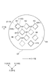
- FIG. 1 is a perspective view of a semiconductor surface light emitting device, with the semiconductor surface light emitting device partially cut away.
- FIG. 2 is a plan view of the basic layer 6A formed on the wafer.
- FIG. 3 is a front view of the wafer.
- FIG. 4 is a view showing an electron micrograph of the basic layer 6A in which holes are formed.
- FIG. 5 is a view showing an optical micrograph of the surface of the semiconductor layer located on the outermost surface side of the semiconductor surface light emitting device.
- FIG. 6 is a diagram showing a detailed configuration of the hole shape.
- FIG. 7 is a cross-sectional view of a semiconductor surface light emitting device.
- FIG. 8 is a cross-sectional view in a direction parallel to the orientation flat of the basic layer 6A.
- FIG. 9 is a cross-sectional view in the direction perpendicular to the orientation flat of the basic layer 6A.
- FIG. 10 is a plan view of the basic layer 6A formed on the wafer according to the first comparative example.
- FIG. 11 is a view showing an electron micrograph of the basic layer 6A in which holes are formed according to the first comparative example.
- FIG. 12 is a view showing an optical micrograph of the surface of the semiconductor layer located on the outermost surface side of the semiconductor surface light emitting device according to the first comparative example.
- FIG. 13 is a diagram showing the concept of crystallinity degradation.
- FIG. 14 is a view showing an electron micrograph of the basic layer 6A in which holes are formed according to the second comparative example.
- FIG. 14 is a view showing an electron micrograph of the basic layer 6A in which holes are formed according to the second comparative example.
- FIG. 15 is an optical micrograph of the surface of the semiconductor layer located on the outermost surface side of the semiconductor surface light emitting device according to the second comparative example.
- FIG. 16 is a diagram for explaining the rotation of the hole direction.
- FIG. 17 shows an electron micrograph of the surface (left side) of the basic layer with the (100) side surface of the hole rotated, and an optical micrograph of the surface (right side) of the semiconductor layer located on the outermost surface side of the semiconductor surface light emitting device.
- FIG. FIG. 18 shows an electron micrograph of the surface (left side) of the basic layer with the (110) side surface of the hole rotated, and an optical micrograph of the surface (right side) of the semiconductor layer located on the outermost surface side of the semiconductor surface light emitting device.
- FIG. 19 shows an electron micrograph of the surface (left side) of the basic layer with the (110) side surface of the hole rotated, and an optical micrograph of the surface (right side) of the semiconductor layer located on the outermost surface side of the semiconductor surface light emitting device.
- FIG. FIG. 20 is a diagram illustrating a shape of a hole in which a part of a corner is notched.
- FIG. 21 is a plan view of the basic layer 6A formed on the wafer.
- FIG. 22 is a diagram showing the shape of the hole.
- FIG. 23 is a diagram showing an electron micrograph of the surface (left side) of the basic layer having a right trapezoidal hole and an optical micrograph of the surface (right side) of the semiconductor layer located on the outermost surface side of the semiconductor surface light emitting device. .
- FIG. 24 is a diagram showing an electron micrograph of the surface (left side) of the basic layer having a right trapezoidal hole and an optical micrograph of the surface of the semiconductor layer (right side) located on the outermost surface side of the semiconductor surface light emitting device.
- FIG. 25 is a diagram showing an electron micrograph of the surface (left side) of the basic layer having a right trapezoidal hole and an optical micrograph of the surface (right side) of the semiconductor layer located on the outermost surface side of the semiconductor surface light emitting device.
- FIG. 26 is a diagram showing a detailed configuration of the hole shape.
- FIG. 27 is a diagram for explaining the rotation of the hole direction.
- FIG. 28 is a diagram showing various hole shapes.
- FIG. 29 is a diagram for explaining a first manufacturing method of the photonic crystal layer.
- FIG. 30 is a diagram for explaining a second manufacturing method of the photonic crystal layer.
- FIG. 1 is a perspective view of a semiconductor surface light emitting device, with the semiconductor surface light emitting device partially broken away.
- the semiconductor surface light emitting device includes a lower clad layer 2, a lower light guide layer 3, an active layer 4, an upper light guide layer 5, a photonic crystal layer 6, an upper clad layer 7, and a contact layer 8 that are sequentially formed on a semiconductor substrate 1. It has. On the back side of the semiconductor substrate 1, an electrode E ⁇ b> 1 is provided on the entire surface, and an electrode E ⁇ b> 2 is provided in the center portion of the contact layer 8.
- the materials / thicknesses of these compound semiconductor layers are as follows. Note that an intrinsic semiconductor having an impurity concentration of 10 15 / cm 3 or less has no conductivity type. Note that the concentration when impurities are added is 10 17 to 10 20 / cm 3 . Further, the following is an example of the present embodiment. If the configuration includes the active layer 4 and the photonic crystal layer 6, the material system, the film thickness, and the layer configuration have flexibility. The numerical values in parentheses are those used in the experiments described later.
- the growth temperature of AlGaAs by the MOCVD method is 500 ° C. to 850 ° C. In the experiments, 550 to 700 ° C. is adopted, and the Al raw material during growth is used.
- TMA trimethylaluminum
- TMG triethylgallium
- TEG triethylgallium
- AsH 3 arsine
- Si 2 H 6 diisilane
- P-type DEZn diethyl zinc
- Contact layer 8 P-type GaAs / 50-500nm (200nm)
- Upper clad layer 7 P-type AlGaAs (Al 0.4 Ga 0.6 As) /1.0 to 3.0 ⁇ m (2.0 ⁇ m)
- Photonic crystal layer 6 Basic layer 6A: GaAs / 50 to 200 nm (100 nm) Buried layer 6B: AlGaAs (Al 0.4 Ga 0.6 As) / 50 to 200 nm (100 nm)
- Upper light guide layer 5 Upper layer: GaAs / 10 to 200 nm (50 nm)
- Lower layer p-type or intrinsic AlGaAs / 10 to 100 nm (50 nm)
- Active layer 4 (multiple quantum well structure): AlGaAs / InGaAs MQW / 10-100nm (30nm)
- Lower light guide layer 3 AlGaAs / 0-300nm (150nm)
- Lower clad layer 2 N-
- FIG. 2 is a plan view of the basic layer 6A formed on the wafer. In the plan view, for the purpose of clarifying the understanding, a plurality of holes H are described which are much larger than the actual scale, and the number thereof is smaller than the actual scale.
- FIG. 3 is a front view of the wafer.
- the main surface of the wafer (substrate) is the (001) plane, and in the drawing, the main surface (001) of the basic layer 6A is exposed on the surface.
- the a-axis, b-axis, and c-axis of the zinc-blende structure crystal are shown in the drawing as the X-axis, Y-axis, and Z-axis, respectively.
- the directions of the X axis, Y axis, and Z axis are [100], [010], and [001], respectively.
- orientation flat OF At one end of the wafer, an orientation flat (hereinafter referred to as orientation flat) OF is formed, and the orientation flat OF is perpendicular to the [110] direction.
- the orientation flat OF has a (-1-10) plane.
- a plurality of holes H (H1 to H10) are formed in the basic layer 6A, and each hole H has a depth in the thickness direction of the semiconductor substrate.
- the outline of the hole H in the planar shape is a rectangle, and each side of the rectangle is inclined 45 degrees with respect to the extending direction [1-10] of the orientation flat OF. That is, the four side surfaces of the hole H have a (100) plane, a (0-10) plane, a (-100) plane, and a (010) plane, respectively. As crystallographically equivalent planes, these planes can be represented as ⁇ 100 ⁇ planes.
- the gravity center positions of the holes H in the plane are arranged at equal intervals along the [1-10] direction, and are also arranged at equal intervals along the [110] direction.
- the former interval for example, between H1 and H2
- the latter interval for example, between H1 and H6
- another hole H4 is positioned on an extension line along the [110] direction of the midpoint position of the former interval (for example, between H1 and H2).
- the interval between the centers of gravity of the holes H in the [1-10] direction is 330 nm, and the interval in the [110] direction is 570 nm.
- the shape of the hole is a rectangle, the length of each side is 165 nm, and the area is 2.7 ⁇ 10 4 nm 2 .
- the line group which connects the gravity center position of the hole H can comprise a square lattice, a rectangular lattice, and a triangular lattice, and may be a random arrangement
- the buried layer 6B shown in FIG. 1 is buried in the hole H of the basic layer 6A, its side surface is in contact with the side surface of the hole H, and its plane orientation matches the plane orientation of the side surface of the hole H. Yes.
- the above-described semiconductor surface light-emitting device has a plurality of holes H periodically formed in the basic layer 6A made of the first compound semiconductor (GaAs) having the zinc flash structure, and the zinc H structure having the zinc flash structure.
- a photonic crystal layer 6 formed by growing a buried layer 6B made of a second compound semiconductor (AlGaAs) is provided.
- AlGaAs second compound semiconductor
- the refractive index of the first compound semiconductor is different from that of the second compound semiconductor.
- a scanning electron microscope (SEM) was used as the electron microscope. The cross-sectional SEM image was taken after the cross-section was stain-etched with ammonia perwater.
- FIG. 4 is a view showing an electron micrograph of the basic layer 6A in which holes are formed.
- FIG. 4A shows a plane photograph of the hole H, and the square hole H is shown.
- FIG. 4B shows a cross-sectional image of the basic layer cut before the orientation flat parallel direction (before formation of the buried layer), and
- FIG. 4C shows the basic layer cut along the orientation flat parallel direction (the buried layer).
- a cross-sectional image before layer formation) is shown.
- 4D shows a cross-sectional image of the basic layer cut after the orientation flat parallel direction (after formation of the buried layer)
- FIG. 4E shows the basic layer cut along the parallel orientation direction of the orientation flat (embedded layer). The cross-sectional image after layer formation is shown.
- the burying process is continued until the upper cladding layer is formed, and then the contact layer is formed. In these buried layers and the upper cladding layer, no large dislocations are observed, and it can be seen that they have good crystallinity.
- FIG. 5 is a diagram showing an optical micrograph of the surface of the semiconductor layer (contact layer) located on the outermost surface side of the semiconductor surface light emitting device in the case of FIG.
- the surface of the contact layer is flat, has excellent morphology, and almost no irregularities are observed. This indirectly indicates that the crystallinity is excellent inside.
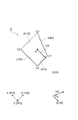
- FIG. 6 is a diagram showing a detailed configuration of the hole shape.
- each side of the rectangle circumscribing the outline of the hole H in the XY plane are L1 and L2.
- a rectangle similar to this rectangle is assumed, and one corner is inscribed.
- the inscribed rectangle has the same center of gravity G as the circumscribed rectangle, and the rotation position in the XY plane is also the same.
- the distances between the corresponding sides are ⁇ L11, ⁇ L12, ⁇ L21, and ⁇ L22, respectively.
- FIG. 7 is a cross-sectional view of a semiconductor surface light emitting device. This example shows a cross section parallel to the orientation flat.
- the semiconductor surface light emitting device includes the lower cladding layer 2, the lower light guide layer 3, the active layer 4, the upper light guide layer 5, the photonic crystal layer 6, and the upper cladding layer that are sequentially formed on the semiconductor substrate 1. 7 and a contact layer 8 are provided.
- the active layer 4 supplies light to the photonic crystal layer 6, and includes upper and lower semiconductor layers 4A and 4C and a central semiconductor layer 4B sandwiched between them.
- the relationship of these energy band gaps is the same as that of a normal laser, and is set so as to have a multiple quantum well structure in which a 4B QW (quantum well) layer is sandwiched between 4A and 4C guide layers.
- the photonic crystal layer 6 is used to generate laser light by light resonance. That is, this semiconductor surface light emitting device is a photonic crystal surface emitting laser, but if the laser oscillation does not occur, the structure can be used as a light emitting diode.
- FIG. 8 is an example of a cross-sectional shape in the initial stage of regrowth embedding in a direction parallel to the orientation flat of the basic layer 6A
- FIG. 9 is an example of a cross-sectional shape in the initial stage of regrowth embedding in a direction perpendicular to the orientation flat of the basic layer 6A. is there.
- each hole H has inclined surfaces (F1 to F8) inclined with respect to the ⁇ 100 ⁇ side surfaces.
- the plane orientations of the inclined surfaces F1 to F8 are (1-11), (-111), (1-13), (-113), (-1-13), (113), (-1-), respectively. 10) and (110).
- FIG. 10 is a plan view of the basic layer 6A formed on the wafer according to the first comparative example. If the semiconductor surface light emitting device shown in FIGS. 1 to 9 is an example, the element of the first comparative example is different from the example only in the shape of the hole H. That is, each side surface of the hole H is constituted by a ⁇ 110 ⁇ plane. Specifically, the respective sides are (110), (1-10), (-1-10), and (-110).
- FIG. 11 is a view showing an electron micrograph of the basic layer 6A in which holes are formed according to the first comparative example.
- FIG. 11A shows a plan view of the hole H, and the square hole H is shown.
- FIG. 11B shows a cross-sectional image of the basic layer cut before the orientation flat parallel direction (before formation of the buried layer), and
- FIG. 11C shows the basic layer cut along the orientation flat parallel direction (embedded layer).
- a cross-sectional image before layer formation) is shown.
- FIG. 11D shows a cross-sectional image of the basic layer cut after the orientation flat parallel direction (after formation of the buried layer), and
- FIG. 11E shows the basic layer cut along the parallel orientation direction of the orientation flat (embedded layer). The cross-sectional image after layer formation is shown.
- the burying process is continued until the upper cladding layer is formed, and then the contact layer is formed. Large dislocations are observed in these buried layers and the upper cladding layer (see FIGS. 11D and 11E), indicating that the crystallinity is not good.
- FIG. 12 is a view showing an optical micrograph of the surface of the semiconductor layer (contact layer) located on the outermost surface side of the semiconductor surface light emitting device according to the first comparative example.
- the surface of the contact layer is rough, the morphology is low, and many irregularities are observed. This indirectly indicates that the crystallinity is poor inside.
- FIG. 13 is a diagram showing the concept of crystallinity degradation.
- the main surface of the basic layer 6A is the (001) plane, and the side surface of the hole H is surrounded by the ⁇ 100 ⁇ plane. Accordingly, the dislocation formation mechanism due to the above (110) and (-1-10) is suppressed, so that the crystallinity is considered to be good.
- FIG. 14 is a view showing an electron micrograph of the basic layer 6A in which holes are formed according to the second comparative example. Only the shape of the hole H is different from the first comparative example, and the others are the same. The opening diameter of the hole H is 120 nm.
- FIG. 14A shows a plane photograph of the hole H, and the circular hole H is shown.
- FIG. 14B shows a cross-sectional image of a basic layer cut before the orientation flat parallel direction (before formation of the buried layer), and
- FIG. 14C shows a basic layer cut along the orientation flat parallel direction (the buried layer).
- a cross-sectional image before layer formation) is shown.
- FIG. 14D shows a cross-sectional image of the basic layer cut after the orientation flat parallel direction (after formation of the buried layer), and
- FIG. 14E shows the basic layer cut along the parallel orientation direction of the orientation flat (embedded layer). The cross-sectional image after layer formation is shown.
- the burying process is continued until the upper cladding layer is formed, and then the contact layer is formed. Large dislocations are not observed in these buried layers and upper cladding layers (see FIGS. 14D and 14E).
- FIG. 15 is a view showing an optical micrograph of the surface of the semiconductor layer located on the outermost surface side of the semiconductor surface light emitting device according to the second comparative example.
- the surface of the contact layer is rough, the morphology deteriorates, and many irregularities are observed. This is because dislocations are not observed in the observation range of FIG. 14, but dislocations are formed when examined in a wider area, leading to deterioration of the surface morphology.
- the hole H according to the embodiment was rotated around the Z axis passing through the center of gravity G, and the tolerance of the rotation angle was investigated.
- FIG. 16 is a diagram for explaining the rotation of the hole direction.
- a perpendicular line is drawn from the center of gravity G in the plane of the hole H toward the one side (010) plane, and an angle formed by the perpendicular line VR and [0-10] is defined as a rotation angle ⁇ . That is, assuming that the hole H has a rectangular shape, a vertical line VR is drawn on one side thereof. When there is a slight fluctuation in the shape of the hole H, a rectangle circumscribing the hole is defined as the shape of the hole H.
- FIG. 17 is an electron micrograph (left side) of the surface of the basic layer obtained by rotating the (100) side face (facet) of the hole according to the example, and the surface of the semiconductor layer located on the outermost surface side of the semiconductor surface light emitting device. It is a figure which shows an optical microscope photograph (right side).
- the length of each side of the square hole is 140 nm, the distance between the centers of gravity of the holes H in the [1-10] direction is 335 nm, and the distance in the [110] direction is 580 nm.
- the rotation angle ⁇ is 35 degrees, the surface morphology is deteriorated, and when ⁇ is smaller than that, the surface morphology is good.
- FIG. 18 is an electron micrograph (left side) of the surface of the basic layer obtained by rotating the (110) side face (face) of the hole according to the first comparative example, and the semiconductor layer located on the outermost surface side of the semiconductor surface light emitting device. It is a figure which shows the optical microscope photograph (right side) of the surface.
- the length of each side of the rectangular hole is 100 nm and 200 nm, the distance between the centers of the holes H in the [1-10] direction is 335 nm, and the short side is parallel to the [1-10] direction.
- the interval in the [110] direction is 580 nm. Since the rotation angle ⁇ is 20 degrees (the rotation angle in the embodiment is 25 degrees), the surface morphology is improved, and when ⁇ is smaller than that, the surface morphology is deteriorated.
- FIG. 19 shows an electron micrograph (left side) of the surface of the basic layer obtained by rotating the (110) side face (facet) of the hole of the first comparative example, and the surface of the semiconductor layer located on the outermost surface side of the semiconductor surface light emitting device. It is a figure which shows the optical microscope photograph (right side). Compared to the case of FIG. 18, the long side is parallel to the [1-10] direction. Since the rotation angle ⁇ is 20 degrees or more (the rotation angle ⁇ in the embodiment is 25 degrees or less), the surface morphology is improved, and when ⁇ is smaller than that, the surface morphology is deteriorated.
- FIG. 20 is a diagram showing the shape of the hole H in which some of the corners C2 and C2 are cut out of the four corners C1 to C4. Since the mechanism of dislocation formation due to (110) and (-1-10) is suppressed, it is considered that the same crystallinity and surface morphology improvement effect as described above can be obtained.
- the shape of the hole H is rectangular, but it may be a right trapezoid.
- FIG. 21 is a plan view of the basic layer 6A formed on the wafer.
- the shape of the hole H is changed to a right trapezoid.
- Other structures are the same as those described above.
- the plane including each side of the right trapezoid is (010), (0-10), (100), (hk0). That is, three side surfaces belong to the ⁇ 100 ⁇ plane.
- FIG. 22 is a diagram showing the shape of the hole H.
- an angle (acute angle) formed by the (010) plane and the (hk0) plane is defined as ⁇ .
- FF represents Filling Factor. Filling factor is an index for measuring the size of the photonic crystal, and is the ratio of the area occupied by the photonic crystal shape (area of the hole H) to the area of the unit period of the two-dimensional structure. In the following example, the length a (lattice constant) per unit period of the two-dimensional structure is 335 nm.
- FIG. 23 shows an electron micrograph of the surface (left side) of the basic layer 6A having a right trapezoidal hole, and an optical micrograph of the surface (right side) of the semiconductor layer (contact layer) located on the outermost surface side of the semiconductor surface light emitting element.
- the ⁇ was changed to 60% and the FF was changed from 11% to 33%, but no significant change was observed in the surface morphology, and both were good.
- FIG. 24 and 25 show an electron micrograph of the surface (left side) of the basic layer having a right trapezoidal hole and an optical micrograph of the surface of the semiconductor layer (right side) located on the outermost surface side of the semiconductor surface light emitting device.
- FIG. 24 and 25 show an electron micrograph of the surface (left side) of the basic layer having a right trapezoidal hole and an optical micrograph of the surface of the semiconductor layer (right side) located on the outermost surface side of the semiconductor surface light emitting device.
- FF was set to 15% (design value) and ⁇ was changed from 30 to 80 degrees, but no significant change was observed in the surface morphology, and all were good.
- FIG. 26 is a diagram showing a detailed configuration of the hole shape.
- the larger dimension of the upper base or the lower base is L1
- the distance between opposing parallel sides is L2.
- a right trapezoid similar to this right trapezoid is assumed, and one corner is inscribed.
- the inscribed right trapezoid has the same center of gravity G as the circumscribed right trapezoid, and the rotation position in the XY plane is also the same.
- the separation distances in the direction parallel to the upper base of the trapezoid of the corresponding side are ⁇ L11 and ⁇ L12
- the separation distances in the trapezoid height direction are ⁇ L21 and ⁇ L22.
- FIG. 27 is a diagram for explaining the rotation of the direction of the hole H in the case of the right trapezoid.
- a perpendicular line is drawn from the center of gravity G in the plane of the hole H toward the one side (010) plane, and the angle formed by the perpendicular line VR and [0-10] is the rotation angle ⁇ .
- a vertical line VR is drawn on one side thereof.
- a rectangle circumscribing the hole is defined as the shape of the hole H.
- the allowable range of the rotation angle ⁇ at which a good crystal is obtained is the same as in the case of the rectangle described above.
- FIG. 28 is a diagram showing various hole shapes.
- FIG. 28A shows the shape of the above-described embodiment.
- (B) a part of one side of (A) is missing and the side surface of the buried layer has a recess (concave surface).
- (C) a part of the two sides of (A) is missing and the side surface of the buried layer has a recess (concave surface).
- (D) a part of the three sides of (A) is missing and the side surface of the buried layer has a recess (concave surface).
- (E) a part of the four sides of (A) is missing and the side surface of the buried layer has a recess (concave surface).
- (G) is a projecting portion (convex surface) shape in which the hypotenuse of the side surface of the buried layer in (A) has two planes.
- the side surface of the buried layer in (A) has a convex (convex) shape in which a large number of planes are continuous.
- the side surface of the buried layer in (A) has a shape in which the hypotenuse has two convex portions (convex surfaces).
- the side surface of the buried layer in (A) has a shape in which one side has a V-groove-shaped recess (concave surface).
- (K) is a convex (convex) shape in which the hypotenuse of the side surface of the buried layer in (A) is curved.
- (L) is a concave (concave) shape in which the hypotenuse of the side surface of the buried layer in (A) is a curved line.
- (M) represents an example of a shape in which the length of one side is an uneven shape formed by a ⁇ 100 ⁇ plane having a length of 5 nm or more, and the shape of the envelope connecting the deepest portion of the concave portion on the side surface is a rectangle.
- the shape of the concavo-convex envelope formed by the ⁇ 100 ⁇ plane is a rectangle in (M)
- it may be an arbitrary shape such as a triangle (N) or a circle (O).
- the side surface of the hole H has at least three different ⁇ 100 ⁇ planes, or a rotational angle of less than ⁇ 35 degrees around these planes about the normal of the main surface. Includes a surface rotated by.
- the surface morphology of the semiconductor layer formed on the photonic crystal layer is very good, the flatness is high, and the amount of dislocation generated inside is relatively high. It can be seen that is decreasing.
- the crystallinity of the semiconductor layer is improved in this manner, the durability due to temperature and heat increases, so that the lifetime can be increased, and the leakage current and internal resistance are reduced, so that the light emission efficiency can be improved. . That is, the characteristics of the semiconductor surface light emitting device can be improved by adopting the hole-shaped configuration described above.
- the side surface of the hole includes four different ⁇ 100 ⁇ faces, or these faces are mainly used as in the embodiment shown in FIGS.
- the surface morphology of the semiconductor layer formed on the photonic crystal layer is very good, and the flatness is The characteristics of the semiconductor surface light emitting device can be improved.
- the rotation angle ⁇ is ⁇ 25 degrees or less
- the surface morphology is remarkably improved and the crystallinity of the semiconductor layer is improved as compared with the case of 35 degrees.
- the rotation angle ⁇ is ⁇ 20 degrees or less
- the surface morphology is further improved as compared with the case of 25 degrees, and the crystallinity of the semiconductor layer is improved.
- the first compound semiconductor is GaAs
- the second compound semiconductor is AlGaAs.
- FIG. 29 is a diagram for explaining a first manufacturing method of the photonic crystal layer.
- a layer (GaAs / AaGaAs) or spacer layer (AlGaAs) 5 and a basic layer (GaAs) 6A to be a photonic crystal layer are epitaxially grown sequentially using MOCVD (metal organic chemical vapor deposition).
- MOCVD metal organic chemical vapor deposition
- a SiN layer AG is formed on the basic layer 6A by PCVD (plasma CVD), and then a resist R is formed on the SiN layer AG (C). Further, the resist R is exposed and developed (D), the SiN layer AG is etched using the resist R as a mask, and a part of the SiN layer AG is left to form an alignment mark (E). The remaining resist is removed (F).
- a resist R2 is applied to the basic layer 6A, a two-dimensional fine pattern is drawn on the resist R2 by an electron beam drawing apparatus, and developed to form a two-dimensional fine pattern on the resist R2 (H). Thereafter, using the resist R2 as a mask, a two-dimensional fine pattern having a depth of about 100 nm is transferred onto the basic layer 6A by dry etching (forming a hole H) (I), and the resist is removed (J). The depth of the hole H is 100 nm.
- the buried layer (AlGaAs) 6B grows in the hole H, and then the P-type cladding layer (AlGaAs) 7 and the P-type contact layer (GaAs) 8 sequentially grow epitaxially (K).
- a resist R3 having a square hole H is formed on the P-type contact 8 (L), the resist R3 is patterned (M), an electrode E is deposited from above the resist R3 (N), and lift-off is performed. The electrode material is removed leaving only the electrode (Cr / Au) E2 (O). Then, the back surface of the N-type semiconductor substrate 1 is polished to form an N-type electrode (AuGe / Au) E1 (P).
- FIG. 30 is a diagram for explaining a second manufacturing method of the photonic crystal layer.
- a layer (GaAs / AaGaAs) or spacer layer (AlGaAs) 5 and a basic layer (GaAs) 6A to be a photonic crystal layer are epitaxially grown sequentially using MOCVD (metal organic chemical vapor deposition).
- MOCVD metal organic chemical vapor deposition
- a resist R2 is applied on the basic layer 6A (B), a two-dimensional fine pattern is drawn with an electron beam drawing apparatus, and developed to form a two-dimensional fine pattern on the resist (C).
- a resist R2 is applied on the basic layer 6A (B)
- a two-dimensional fine pattern is drawn with an electron beam drawing apparatus, and developed to form a two-dimensional fine pattern on the resist (C).
- squares with sides of 120 nm surrounded by (110) Facets are arranged at 330 nm intervals at the alignment mark position of the photomask to be used, and the area of the entire region is set to 100 ⁇ m ⁇ 100 ⁇ m.
- this pattern is used as a reference for alignment of optical exposure after regrowth.
- a two-dimensional fine pattern having a depth of about 100 nm is transferred onto the basic layer 6A by dry etching (D), and the resist is removed (E). Since the mark position is also etched, a pattern (alignment mark) is formed at this position.
- This pattern has side surfaces surrounded by four ⁇ 110 ⁇ planes, but may be rotated slightly (within ⁇ 10 degrees). In this pattern, dislocations are formed even by regrowth, so that the regrowth surface becomes rough. Therefore, the rough surface can be used as a reference for alignment in optical exposure after regrowth. Thereafter, regrowth is performed using the MOCVD method.
- the ⁇ 110 ⁇ plane or ⁇ 110 ⁇ was rotated by a rotation angle within ⁇ 10 degrees around the normal line of the main surface (001) by etching.
- the alignment mark including the surface in an appropriate location (outside area of the light emitting element formation scheduled area) of the semiconductor substrate on which the basic layer 6A is formed, the normal alignment mark forming process can be omitted.
- the buried layer (AlGaAs) 6B grows in the hole H, and then the P-type cladding layer (AlGaAs) 7 and the P-type contact layer (GaAs) 8 grow epitaxially in sequence (F).
- a resist R3 having a square hole H is formed on the P-type contact 8 (G), the resist R3 is patterned by optical exposure (H), and an electrode E is deposited on the resist R3 (I). Then, by lift-off, the electrode material is removed leaving only the electrode (Cr / Au) E2 (J). Then, the back surface of the N-type semiconductor substrate 1 is polished to form an N-type electrode (AuGe / Au) E1 (K).
- the depth of the hole H may be shallower than the basic layer 6A, or may be slightly deeper.
- the (001) wafer may be an off-substrate.
- the manufacturing method using the electron beam exposure method has been described as the method for manufacturing the hole H.
- other fine processing techniques such as nanoimprint, interference exposure, optical exposure such as FIB, and stepper may be used.
- 6A basic layer
- 6B buried layer
- H hole.
Landscapes
- Physics & Mathematics (AREA)
- Optics & Photonics (AREA)
- Engineering & Computer Science (AREA)
- Condensed Matter Physics & Semiconductors (AREA)
- Electromagnetism (AREA)
- General Physics & Mathematics (AREA)
- Chemical & Material Sciences (AREA)
- Nanotechnology (AREA)
- Crystallography & Structural Chemistry (AREA)
- Biophysics (AREA)
- Life Sciences & Earth Sciences (AREA)
- Manufacturing & Machinery (AREA)
- Computer Hardware Design (AREA)
- Microelectronics & Electronic Packaging (AREA)
- Power Engineering (AREA)
- Semiconductor Lasers (AREA)
- Led Devices (AREA)
Abstract
Description
・コンタクト層8:
P型のGaAs/50~500nm(200nm)
・上部クラッド層7:
P型のAlGaAs(Al0.4Ga0.6As)/1.0~3.0μm(2.0μm)
・フォトニック結晶層6:
基本層6A:GaAs/50~200nm(100nm)
埋め込み層6B:AlGaAs(Al0.4Ga0.6As)/50~200nm(100nm)
・上部光ガイド層5:
上層:GaAs/10~200nm(50nm)
下層:p型または真性のAlGaAs/10~100nm(50nm)
・活性層4(多重量子井戸構造):
AlGaAs/InGaAs MQW/10~100nm(30nm)
・下部光ガイド層3:
AlGaAs/0~300nm(150nm)
・下部クラッド層2:
N型のAlGaAs/1.0~3.0μm(2.0μm)
・半導体基板1:
N型のGaAs/80~350μm(200μm) The materials / thicknesses of these compound semiconductor layers are as follows. Note that an intrinsic semiconductor having an impurity concentration of 10 15 / cm 3 or less has no conductivity type. Note that the concentration when impurities are added is 10 17 to 10 20 / cm 3 . Further, the following is an example of the present embodiment. If the configuration includes the
Contact layer 8:
P-type GaAs / 50-500nm (200nm)
Upper clad layer 7:
P-type AlGaAs (Al 0.4 Ga 0.6 As) /1.0 to 3.0 μm (2.0 μm)
Photonic crystal layer 6:
Upper light guide layer 5:
Upper layer: GaAs / 10 to 200 nm (50 nm)
Lower layer: p-type or intrinsic AlGaAs / 10 to 100 nm (50 nm)
Active layer 4 (multiple quantum well structure):
AlGaAs / InGaAs MQW / 10-100nm (30nm)
Lower light guide layer 3:
AlGaAs / 0-300nm (150nm)
Lower clad layer 2:
N-type AlGaAs / 1.0-3.0μm (2.0μm)
・ Semiconductor substrate 1:
N-type GaAs / 80-350μm (200μm)
Claims (7)
- 閃亜鉛構造の第1化合物半導体からなる基本層内に複数の穴を周期的に形成し、前記穴内に、閃亜鉛構造であって第2化合物半導体からなる埋め込み層を成長させてなるフォトニック結晶層と、
前記フォトニック結晶層に対して光を供給する活性層と、
を備え、
前記基本層の主表面は(001)面であり、
前記穴の側面は、少なくとも異なる3つの{100}面、又は、これらの面を前記主表面の法線の回りに±35度未満の回転角度で回転させた面を含んでいる、
ことを特徴とする半導体面発光素子。 A photonic crystal in which a plurality of holes are periodically formed in a basic layer made of a first compound semiconductor having a zinc flash structure, and a buried layer made of a second compound semiconductor having a zinc flash structure is grown in the hole. Layers,
An active layer for supplying light to the photonic crystal layer;
With
The main surface of the basic layer is a (001) plane,
The side surface of the hole includes at least three different {100} planes, or planes obtained by rotating these planes around a normal of the main surface with a rotation angle of less than ± 35 degrees.
A semiconductor surface light emitting device. - 前記穴の側面は、
4つの異なる{100}面、又は、
これらの面を前記主表面の法線に回りに±35度未満の回転角度で回転させた面
を含んでいる、
ことを特徴とする請求項1に記載の半導体面発光素子。 The side surface of the hole is
4 different {100} faces, or
Including a face rotated around the normal of the main surface at a rotation angle of less than ± 35 degrees,
The semiconductor surface light emitting device according to claim 1. - 前記回転角度は、±25度以下に設定されている、
ことを特徴とする請求項1又は2に記載の半導体面発光素子。 The rotation angle is set to ± 25 degrees or less,
The semiconductor surface-emitting device according to claim 1 or 2, - 前記回転角度は、±20度以下に設定されている、
ことを特徴とする請求項1又は2に記載の半導体面発光素子。 The rotation angle is set to ± 20 degrees or less,
The semiconductor surface-emitting device according to claim 1 or 2, - 前記第1化合物半導体はGaAsであり、
前記第2化合物半導体はAlGaAsである、
ことを特徴とする請求項1乃至4のいずれか1項に記載の半導体面発光素子。 The first compound semiconductor is GaAs;
The second compound semiconductor is AlGaAs;
The semiconductor surface light-emitting device according to claim 1, wherein the semiconductor surface light-emitting device is provided. - 請求項1乃至5のいずれか1項に記載の半導体面発光素子を製造する半導体面発光素子の製造方法において、
前記穴を形成する工程と、
前記埋め込み層の成長を行う工程と、
を備えることを特徴とする半導体面発光素子の製造方法。 In the manufacturing method of the semiconductor surface light emitting element which manufactures the semiconductor surface light emitting element of any one of Claims 1 thru | or 5,
Forming the hole;
Growing the buried layer;
A method for manufacturing a semiconductor surface light emitting device, comprising: - 前記成長を行う工程の前に、エッチングにより{110}面、又は{110}を前記主表面の法線回りに±10度以内の回転角度で回転させた面を含むアライメントマークを、前記基本層の形成される半導体基板に形成する工程
を備えることを特徴とする請求項6に記載の半導体面発光素子の製造方法。 Before the step of performing the growth, an alignment mark including a {110} plane or a plane obtained by rotating {110} at a rotation angle within ± 10 degrees around the normal of the main surface by etching is used as the base layer. The method of manufacturing a semiconductor surface light emitting device according to claim 6, further comprising a step of forming the semiconductor substrate on the semiconductor substrate on which the semiconductor surface is formed.
Priority Applications (3)
| Application Number | Priority Date | Filing Date | Title |
|---|---|---|---|
| US13/812,561 US8693516B2 (en) | 2010-07-30 | 2011-06-21 | Semiconductor surface light-emitting element and method of manufacturing thereof |
| DE112011102549.1T DE112011102549B4 (en) | 2010-07-30 | 2011-06-21 | LIGHT-EMITTING SEMICONDUCTOR SURFACE ELEMENT AND THEIR PRODUCTION METHOD |
| CN201180037546.9A CN103038959B (en) | 2010-07-30 | 2011-06-21 | Semiconductor surface light-emitting component and its manufacture method |
Applications Claiming Priority (2)
| Application Number | Priority Date | Filing Date | Title |
|---|---|---|---|
| JP2010172578A JP5549011B2 (en) | 2010-07-30 | 2010-07-30 | Semiconductor surface light emitting device and manufacturing method thereof |
| JP2010-172578 | 2010-07-30 |
Publications (1)
| Publication Number | Publication Date |
|---|---|
| WO2012014604A1 true WO2012014604A1 (en) | 2012-02-02 |
Family
ID=45529824
Family Applications (1)
| Application Number | Title | Priority Date | Filing Date |
|---|---|---|---|
| PCT/JP2011/064181 WO2012014604A1 (en) | 2010-07-30 | 2011-06-21 | Semiconductor surface light-emitting element and method of manufacturing thereof |
Country Status (5)
| Country | Link |
|---|---|
| US (1) | US8693516B2 (en) |
| JP (1) | JP5549011B2 (en) |
| CN (1) | CN103038959B (en) |
| DE (1) | DE112011102549B4 (en) |
| WO (1) | WO2012014604A1 (en) |
Cited By (4)
| Publication number | Priority date | Publication date | Assignee | Title |
|---|---|---|---|---|
| JPS6358313A (en) * | 1986-08-29 | 1988-03-14 | Koputeitsuku:Kk | Soft focus lens |
| WO2014136653A1 (en) * | 2013-03-04 | 2014-09-12 | 国立大学法人京都大学 | Semiconductor laser element |
| US9307458B1 (en) | 2014-03-24 | 2016-04-05 | Sprint Spectrum L.P. | Controlling reverse-direction neighbor reports based on the characteristics of queued bearer traffic |
| WO2017150160A1 (en) * | 2016-02-29 | 2017-09-08 | 国立大学法人京都大学 | Heat-radiating light source |
Families Citing this family (17)
| Publication number | Priority date | Publication date | Assignee | Title |
|---|---|---|---|---|
| US9110316B2 (en) * | 2011-12-01 | 2015-08-18 | Samsung Electronics Co., Ltd. | Method of amplifying magneto-optical kerr effect by using photon crystal structures, and photon crystal having amplified magneto-optical kerr effect, method of fabricating photon crystal |
| US10938177B2 (en) | 2014-08-29 | 2021-03-02 | Kyoto University | Two-dimensional photonic crystal surface emitting laser |
| US10461501B2 (en) | 2014-08-29 | 2019-10-29 | Kyoto University | Two-dimensional photonic crystal surface emitting laser |
| WO2016148075A1 (en) * | 2015-03-13 | 2016-09-22 | 浜松ホトニクス株式会社 | Semiconductor light emitting element |
| JP6747910B2 (en) * | 2016-08-10 | 2020-08-26 | 浜松ホトニクス株式会社 | Light emitting device |
| US11031751B2 (en) | 2016-08-10 | 2021-06-08 | Hamamatsu Photonics K.K. | Light-emitting device |
| US10734786B2 (en) | 2016-09-07 | 2020-08-04 | Hamamatsu Photonics K.K. | Semiconductor light emitting element and light emitting device including same |
| JP7101370B2 (en) * | 2017-02-27 | 2022-07-15 | 国立大学法人京都大学 | Manufacturing method of surface emitting laser and surface emitting laser |
| US11646546B2 (en) | 2017-03-27 | 2023-05-09 | Hamamatsu Photonics K.K. | Semiconductor light emitting array with phase modulation regions for generating beam projection patterns |
| US11637409B2 (en) * | 2017-03-27 | 2023-04-25 | Hamamatsu Photonics K.K. | Semiconductor light-emitting module and control method therefor |
| JP6959042B2 (en) | 2017-06-15 | 2021-11-02 | 浜松ホトニクス株式会社 | Light emitting device |
| JP6355178B2 (en) * | 2017-06-29 | 2018-07-11 | 国立大学法人京都大学 | Laser equipment |
| DE112018006285T5 (en) | 2017-12-08 | 2021-01-28 | Hamamatsu Photonics K.K. | LIGHT EMITTING DEVICE AND MANUFACTURING METHOD FOR IT |
| JP7279875B2 (en) * | 2018-09-03 | 2023-05-23 | 国立大学法人京都大学 | Surface-emitting laser element and method for manufacturing surface-emitting laser element |
| US20230035423A1 (en) * | 2019-12-27 | 2023-02-02 | Hamamatsu Photonics K.K. | Spatial light modulator and light-emitting device |
| CN113991424B (en) * | 2021-10-22 | 2024-01-02 | 清华大学 | High-power unilateral light-emitting semiconductor laser based on inclined surface grating |
| DE102022101787A1 (en) * | 2022-01-26 | 2023-07-27 | OSRAM Opto Semiconductors Gesellschaft mit beschränkter Haftung | LASER DIODE DEVICE AND METHOD OF MAKING AT LEAST ONE PHOTONIC CRYSTAL STRUCTURE FOR A LASER DIODE DEVICE |
Citations (3)
| Publication number | Priority date | Publication date | Assignee | Title |
|---|---|---|---|---|
| JP2006156944A (en) * | 2004-10-25 | 2006-06-15 | Ricoh Co Ltd | Photonic crystal laser, method of manufacturing photonic crystal laser, surface emitting laser array, light transmission system, and writing system |
| JP2006258865A (en) * | 2005-03-15 | 2006-09-28 | Ricoh Co Ltd | Optical component and manufacturing method thereof |
| JP2008506269A (en) * | 2004-07-08 | 2008-02-28 | イオン オプティクス インコーポレイテッド | Tunable photonic crystal |
Family Cites Families (6)
| Publication number | Priority date | Publication date | Assignee | Title |
|---|---|---|---|---|
| US6259114B1 (en) * | 1999-05-07 | 2001-07-10 | International Business Machines Corporation | Process for fabrication of an all-epitaxial-oxide transistor |
| JP5376104B2 (en) * | 2005-07-04 | 2013-12-25 | ソニー株式会社 | Surface emitting semiconductor laser |
| US20070030873A1 (en) * | 2005-08-03 | 2007-02-08 | Finisar Corporation | Polarization control in VCSELs using photonics crystals |
| JP2007258261A (en) * | 2006-03-20 | 2007-10-04 | Kyoto Univ | Two-dimensional photonic crystal surface-emitting laser |
| JP5266789B2 (en) | 2008-02-26 | 2013-08-21 | 住友電気工業株式会社 | Semiconductor laser device and manufacturing method thereof |
| JP5376360B2 (en) | 2008-11-10 | 2013-12-25 | 住友電気工業株式会社 | Method for manufacturing photonic crystal surface emitting laser |
-
2010
- 2010-07-30 JP JP2010172578A patent/JP5549011B2/en active Active
-
2011
- 2011-06-21 WO PCT/JP2011/064181 patent/WO2012014604A1/en active Application Filing
- 2011-06-21 CN CN201180037546.9A patent/CN103038959B/en active Active
- 2011-06-21 US US13/812,561 patent/US8693516B2/en active Active
- 2011-06-21 DE DE112011102549.1T patent/DE112011102549B4/en active Active
Patent Citations (3)
| Publication number | Priority date | Publication date | Assignee | Title |
|---|---|---|---|---|
| JP2008506269A (en) * | 2004-07-08 | 2008-02-28 | イオン オプティクス インコーポレイテッド | Tunable photonic crystal |
| JP2006156944A (en) * | 2004-10-25 | 2006-06-15 | Ricoh Co Ltd | Photonic crystal laser, method of manufacturing photonic crystal laser, surface emitting laser array, light transmission system, and writing system |
| JP2006258865A (en) * | 2005-03-15 | 2006-09-28 | Ricoh Co Ltd | Optical component and manufacturing method thereof |
Cited By (9)
| Publication number | Priority date | Publication date | Assignee | Title |
|---|---|---|---|---|
| JPS6358313A (en) * | 1986-08-29 | 1988-03-14 | Koputeitsuku:Kk | Soft focus lens |
| WO2014136653A1 (en) * | 2013-03-04 | 2014-09-12 | 国立大学法人京都大学 | Semiconductor laser element |
| JP2014197659A (en) * | 2013-03-04 | 2014-10-16 | 国立大学法人京都大学 | Semiconductor laser element |
| US9583914B2 (en) | 2013-03-04 | 2017-02-28 | Kyoto University | Semiconductor laser element |
| US9307458B1 (en) | 2014-03-24 | 2016-04-05 | Sprint Spectrum L.P. | Controlling reverse-direction neighbor reports based on the characteristics of queued bearer traffic |
| US9973982B1 (en) | 2014-03-24 | 2018-05-15 | Sprint Spectrum L.P. | Controlling reverse-direction neighbor reports based on the characteristics of queued bearer traffic |
| WO2017150160A1 (en) * | 2016-02-29 | 2017-09-08 | 国立大学法人京都大学 | Heat-radiating light source |
| JPWO2017150160A1 (en) * | 2016-02-29 | 2019-01-10 | 国立大学法人京都大学 | Thermal radiation light source |
| US10777972B2 (en) | 2016-02-29 | 2020-09-15 | Kyoto University | Thermal radiation light source |
Also Published As
| Publication number | Publication date |
|---|---|
| DE112011102549T5 (en) | 2013-05-02 |
| DE112011102549B4 (en) | 2020-06-18 |
| US20130121358A1 (en) | 2013-05-16 |
| JP2012033747A (en) | 2012-02-16 |
| CN103038959B (en) | 2015-08-12 |
| US8693516B2 (en) | 2014-04-08 |
| JP5549011B2 (en) | 2014-07-16 |
| CN103038959A (en) | 2013-04-10 |
Similar Documents
| Publication | Publication Date | Title |
|---|---|---|
| JP5549011B2 (en) | Semiconductor surface light emitting device and manufacturing method thereof | |
| JP5140962B2 (en) | Manufacturing method of nitride semiconductor substrate | |
| EP3849031B1 (en) | Surface emitting laser element and manufacturing method of the same | |
| US20230127863A1 (en) | Surface-emitting laser element and surface-emitting laser element manufacturing method | |
| JP2006036561A (en) | Method for growing semiconductor crystal, optical semiconductor element, and substrate for crystal growth | |
| US6469320B2 (en) | Semiconductor light emitting device | |
| JP2003332618A (en) | Semiconductor light emitting element | |
| JP5488916B2 (en) | Semiconductor surface light emitting device and manufacturing method thereof | |
| JP2007281140A (en) | Compound semiconductor substrate, manufacturing method thereof, and semiconductor device | |
| US10461222B2 (en) | Light-emitting element comprising sapphire substrate with convex portions | |
| JP2009141085A (en) | Nitride semiconductor device | |
| JP4844086B2 (en) | Semiconductor manufacturing method and satellite | |
| JP5488917B2 (en) | Semiconductor surface light emitting device and manufacturing method thereof | |
| JP2001156403A (en) | Iii-family nitride-system compound semiconductor laser diode | |
| US20120273794A1 (en) | Semiconductor light emitting device, wafer, and method for manufacturing semiconductor light emitting device | |
| JP4623799B2 (en) | Semiconductor light emitting device manufacturing method and semiconductor laser | |
| US6855571B1 (en) | Method of producing GaN-based semiconductor laser device and semiconductor substrate used therefor | |
| JP5003719B2 (en) | Semiconductor device and crystal growth substrate | |
| JP2004007009A (en) | Manufacturing method of nitride semiconductor device | |
| JP5454647B2 (en) | Nitride semiconductor substrate manufacturing method, nitride semiconductor substrate, and light emitting device | |
| JP2023114774A (en) | Semiconductor light-emitting element | |
| JP5810482B2 (en) | Manufacturing method of optical semiconductor device | |
| JPH04113685A (en) | Manufacture of semiconductor device | |
| JPH09214056A (en) | Fabrication method of semiconductor device, semiconductor laser and its fabrication method | |
| JP2007184432A (en) | Method of manufacturing semiconductor stack structure, and semiconductor element formed thereon |
Legal Events
| Date | Code | Title | Description |
|---|---|---|---|
| WWE | Wipo information: entry into national phase |
Ref document number: 201180037546.9 Country of ref document: CN |
|
| 121 | Ep: the epo has been informed by wipo that ep was designated in this application |
Ref document number: 11812197 Country of ref document: EP Kind code of ref document: A1 |
|
| WWE | Wipo information: entry into national phase |
Ref document number: 13812561 Country of ref document: US |
|
| WWE | Wipo information: entry into national phase |
Ref document number: 1120111025491 Country of ref document: DE Ref document number: 112011102549 Country of ref document: DE |
|
| 122 | Ep: pct application non-entry in european phase |
Ref document number: 11812197 Country of ref document: EP Kind code of ref document: A1 |