WO2012014551A1 - 分子間相互作用の検出装置及び検出方法 - Google Patents
分子間相互作用の検出装置及び検出方法 Download PDFInfo
- Publication number
- WO2012014551A1 WO2012014551A1 PCT/JP2011/061369 JP2011061369W WO2012014551A1 WO 2012014551 A1 WO2012014551 A1 WO 2012014551A1 JP 2011061369 W JP2011061369 W JP 2011061369W WO 2012014551 A1 WO2012014551 A1 WO 2012014551A1
- Authority
- WO
- WIPO (PCT)
- Prior art keywords
- light
- white light
- detector
- light transmission
- transmission path
- Prior art date
Links
Images


Classifications
-
- G—PHYSICS
- G01—MEASURING; TESTING
- G01N—INVESTIGATING OR ANALYSING MATERIALS BY DETERMINING THEIR CHEMICAL OR PHYSICAL PROPERTIES
- G01N21/00—Investigating or analysing materials by the use of optical means, i.e. using sub-millimetre waves, infrared, visible or ultraviolet light
- G01N21/17—Systems in which incident light is modified in accordance with the properties of the material investigated
- G01N21/55—Specular reflectivity
- G01N21/552—Attenuated total reflection
- G01N21/553—Attenuated total reflection and using surface plasmons
-
- G—PHYSICS
- G01—MEASURING; TESTING
- G01N—INVESTIGATING OR ANALYSING MATERIALS BY DETERMINING THEIR CHEMICAL OR PHYSICAL PROPERTIES
- G01N21/00—Investigating or analysing materials by the use of optical means, i.e. using sub-millimetre waves, infrared, visible or ultraviolet light
- G01N21/75—Systems in which material is subjected to a chemical reaction, the progress or the result of the reaction being investigated
- G01N21/77—Systems in which material is subjected to a chemical reaction, the progress or the result of the reaction being investigated by observing the effect on a chemical indicator
-
- G—PHYSICS
- G01—MEASURING; TESTING
- G01N—INVESTIGATING OR ANALYSING MATERIALS BY DETERMINING THEIR CHEMICAL OR PHYSICAL PROPERTIES
- G01N21/00—Investigating or analysing materials by the use of optical means, i.e. using sub-millimetre waves, infrared, visible or ultraviolet light
- G01N21/17—Systems in which incident light is modified in accordance with the properties of the material investigated
- G01N21/55—Specular reflectivity
-
- G—PHYSICS
- G01—MEASURING; TESTING
- G01N—INVESTIGATING OR ANALYSING MATERIALS BY DETERMINING THEIR CHEMICAL OR PHYSICAL PROPERTIES
- G01N21/00—Investigating or analysing materials by the use of optical means, i.e. using sub-millimetre waves, infrared, visible or ultraviolet light
- G01N21/75—Systems in which material is subjected to a chemical reaction, the progress or the result of the reaction being investigated
- G01N21/77—Systems in which material is subjected to a chemical reaction, the progress or the result of the reaction being investigated by observing the effect on a chemical indicator
- G01N2021/7769—Measurement method of reaction-produced change in sensor
- G01N2021/7773—Reflection
-
- G—PHYSICS
- G01—MEASURING; TESTING
- G01N—INVESTIGATING OR ANALYSING MATERIALS BY DETERMINING THEIR CHEMICAL OR PHYSICAL PROPERTIES
- G01N21/00—Investigating or analysing materials by the use of optical means, i.e. using sub-millimetre waves, infrared, visible or ultraviolet light
- G01N21/75—Systems in which material is subjected to a chemical reaction, the progress or the result of the reaction being investigated
- G01N21/77—Systems in which material is subjected to a chemical reaction, the progress or the result of the reaction being investigated by observing the effect on a chemical indicator
- G01N2021/7769—Measurement method of reaction-produced change in sensor
- G01N2021/7779—Measurement method of reaction-produced change in sensor interferometric
Definitions
- the present invention relates to an intermolecular interaction detection apparatus and detection method, and more particularly to a detection apparatus and detection method for detecting intermolecular interactions such as biomolecules and organic polymers.
- the detector 100 shown in FIGS. 15A to 15C is used in this method.
- the detector 100 has a substrate 102, and an optical thin film 104 is provided on the substrate 102.
- the spectral intensity of the white light itself is represented by a solid line 106
- the spectral intensity of the reflected light is represented by a solid line 108, as shown in FIG.
- a reflection spectrum 110 represented by a solid line is obtained as shown in FIG.
- the ligand 120 is provided on the optical thin film 104 as shown in FIG. 15B.
- the optical thickness 112 changes, the optical path length changes, and the interference wavelength also changes. That is, the peak position of the spectral intensity distribution of the reflected light is shifted, and as a result, the reflected spectrum 110 is shifted to the reflected spectrum 122 (see the dotted line portion) as shown in FIG.
- the ligand 120 of the detector 100 and the analyte 130 in the sample solution are combined as shown in FIG. 15C.
- the optical thickness 112 is further changed, and the reflection spectrum 122 is shifted to the reflection spectrum 132 (see the one-dot chain line portion) as shown in FIG.
- the intermolecular interaction can be detected by detecting the amount of change between the peak wavelength (bottom peak wavelength) of the reflection spectrum 122 and the bottom peak wavelength of the reflection spectrum 132.
- the change in the bottom peak wavelength due to the ligand 120 can be confirmed at the time point 140.
- the ligand 120, the analyte 130, The change of the bottom peak wavelength due to the coupling of can be confirmed.
- the conventional intermolecular interaction measuring device using the RIfS method generally has a spectroscope for detecting reflected light so that the white light reflected from the light source to the detector substrate is received. This path is formed, and the path for receiving white light directly from the light source is not provided. For this reason, the wavelength distribution characteristics of the spectral intensity of the white light used as a reference for obtaining the reflection spectrum are preliminarily measured at the time of device assembly adjustment as data (hereinafter referred to as reference data), and the actual specimen is detected. The actual situation is that the reference data is sometimes read out and used to calculate the reflection spectrum.
- the reference data for the wavelength distribution characteristics prepared in advance does not take into account the temperature characteristics of the light source at the time of detecting the specimen or the wavelength distribution characteristics of the light source intensity with respect to aging, the reference data is used.
- the reflection spectrum of the reflected light is obtained, there is a problem that the detection accuracy is lowered due to the influence of the temperature characteristics of the light source and aging deterioration.
- the object of the present invention is to improve detection accuracy when detecting intermolecular interactions.
- a detector having a ligand; A white light source that emits white light; A spectroscope that detects the spectral intensity of the received light; From the white light source, a first light transmission path for transmitting white light from the white light source to the detector, a second light transmission path for transmitting reflected white light from the detector to the spectroscope, and the white light source A light transmission part having a third light transmission path for transmitting white light to the spectrometer; A reflected light receiving state that enables transmission of reflected light of white light at the detector by the first and second light transmission paths to the spectrometer, and from the white light source by the third light transmission path A switching unit that switches between a white light receiving state that enables transmission of white light to the detector; A control unit that controls the switching unit and the spectroscope to detect a spectral intensity in each of the white light receiving state and the reflected light receiving state.
- a detection device is provided.
- the detection device obtains a reflection spectrum by calculating a reflectance for each predetermined wavelength interval based on the spectral intensity of the white light and the spectral intensity of the reflected light obtained by the control of the control unit.
- a calculation part can be provided.
- the switching unit of the detection device includes a shielding body that performs position switching, a shielding state of light transmission by the first light transmission path, and a shielding state of light transmission by the second or third light transmission path.
- the shutter mechanism can be switched selectively.
- the switching unit of the detection device can selectively switch between a light transmission shielding state by the first light transmission path and a light transmission shielding state by the second or third light transmission path. It can be.
- a detector having a ligand; a white light source that emits white light; a spectroscope that detects a spectral intensity of received light; and a first light transmission path that transmits white light from the white light source to the detector;
- a light transmission unit having a second light transmission path for transmitting the reflected light of the white light from the detector to the spectrometer and a third light transmission path for transmitting white light from the white light source to the spectrometer;
- a detection method for detecting an intermolecular interaction using a detection apparatus comprising: A first detection step of receiving white light reflected by the detector through the first and second light transmission paths and detecting the spectral intensity thereof by the spectrometer; Before and after the first detection step, a second detection step of receiving white light from the white light source through the third light transmission path and detecting the spectral intensity by the spectroscope, Based on the spectral intensity of the white light and the spectral intensity of the reflected light obtained by the first detection step and
- the white light can be transmitted from the white light source to the spectroscope using the third light transmission path of the light transmitting unit, when detecting the spectral intensity from the reflected light of the detector, The spectral intensity of the reference white light can also be detected without separating them. As a result, it is possible to detect the spectral intensity of each of the white light and reflected light in a state where the influence of the temperature change and aging deterioration of the white light source is almost equal, and to obtain the reflection spectrum, so that the measurement accuracy can be improved as compared with the past. It becomes possible.
- the switching unit exists in the non-shielded state because the shield is retracted from the light transmission path. It is possible to realize good light transmission without hindering light transmission.
- a shielding region corresponding to an arbitrary shape can be formed even if the cross section of the two light transmission paths has a complex structure. It is possible to realize switching of the light transmission path. In addition, it is possible to realize switching of the respective light transmission paths without arranging the two light transmission paths to be switched apart from each other.
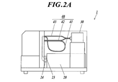
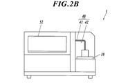
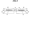
- FIG. 1 shows schematic structure of the detection apparatus of an intermolecular interaction. It is a right view of the detection apparatus which removed the upper frame and cover of the apparatus, and was able to see the internal structure. It is the left view of the detection apparatus which removed the upper frame and cover of the apparatus, and was able to see the internal structure. It is a block block diagram of the detection apparatus of an intermolecular interaction. It is drawing which shows schematic structure of a detector. It is drawing which shows the end surface by the side of the detector by which the 1st optical fiber and the 2nd optical fiber were combined. It is drawing which shows the edge part by the side of the spectrometer by which the 2nd optical fiber and the 3rd optical fiber were combined.
- FIG. 1 is a schematic diagram schematically illustrating the configuration of an intermolecular interaction detection device 1 according to an embodiment of the present invention
- FIG. 2A is a detection device in which the upper frame and cover are removed to make the internal configuration visible
- 1B is a left side view
- FIG. 3 is a functional block diagram of the detection apparatus 1.
- the detection device 1 mainly includes a detector 10, a white light source 20, a spectroscope 30, a light transmission unit 40, a switching unit 80, a temperature control unit 90, a control device 50, and the like. Has been.
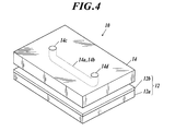
- the detector 10 basically includes a sensor chip 12 and a flow cell 14. As shown in FIG. 4, the sensor chip 12 has a silicon substrate 12a having a rectangular shape. A SiN film 12b (silicon nitride) is deposited on the silicon substrate 12a. The SiN film 12b is an example of an optical thin film.
- the flow cell 14 is a transparent member made of silicone rubber. A groove 14 a is formed in the flow cell 14. When the flow cell 14 is brought into close contact with the sensor chip 12, a sealed channel 14b is formed (see FIG. 1). Both end portions of the groove 14a are exposed from the surface of the flow cell 14, one end portion is connected to the liquid feeding portion 17 and functions as an inlet 14c to which a sample solution is supplied, and the other end portion is a waste liquid portion 18. To function as a sample solution outlet 14d. A ligand 16 is bound to the bottom of the groove 14a of the flow cell 14 (see FIG. 1).
- the flow cell 14 can be replaced with the sensor chip 12, and the flow cell 14 can be used in a disposable manner.
- the surface of the sensor chip 12 may be modified with a silane coupling agent or the like. In this case, the flow cell 14 can be easily replaced.
- first and second optical fibers 41 and 42 which will be described later, are installed in close contact with each other on the upper surface of the flow cell 14 and above the sealed flow path 14b.
- the first optical fiber 41 is for guiding the white light emitted from the white light source 20 to the flow cell 14, and when the white light source 20 is turned on, the white light is sealed through the first optical fiber 41. Irradiate the path 14b.
- the second optical fiber 42 is for guiding light from the flow cell 14 to the spectroscope 30, and detects reflected light when the white light of the white light source 20 irradiates the sealed flow path 14 b to the spectroscope 30. It is possible to do.
- the temperature control unit 90 includes, for example, a temperature adjustment element that performs heating and cooling, such as a Peltier element, and a temperature detection element, and these are provided in the detector 10. And the control apparatus 50 detects the temperature of the detector 10 with a temperature detection element through the microcomputer 52 mentioned later, and performs temperature control so that it may become preset temperature by the heating or cooling by a temperature control element.
- the light transmission unit 40 includes a first optical fiber 41 as a first light transmission path for guiding white light from the white light source 20 to the closed flow path 14 b of the flow cell 14, and white light from the first optical fiber 41.
- a second optical fiber 42 as a second light transmission path for guiding reflected light by light irradiation from the closed flow path 14 b of the flow cell 1 to the spectrometer 30, and white light from the white light source 20 directly on the spectrometer 30.
- a third optical fiber 43 as a third light transmission path for guiding the light to the light source.
- each of the optical fibers 41 to 43 has a structure in which fine fibers are bundled. And the edge part by the side of the flow cell 14 of the 1st optical fiber 41 and the 2nd optical fiber 42 is compounded closely so that each fine fiber may become one bundle, as shown in FIG. .
- the fine fibers 41 a constituting the first optical fiber 41 are distributed in the center on the end face on the flow cell 14 side, and the fine fibers 42 a constituting the second optical fiber 42 are the fine fibers of the first optical fiber 41. It is distributed around the bundle so as to surround it.
- FIG. 5 only the fine fibers of the first optical fiber 41 are shown in color so that the respective fine fibers 41a and 42a can be identified, but in actuality, both of the fine fibers 41a and 42a are colorless and transparent. It is.
- the end portions of the second optical fiber 42 and the third optical fiber 43 on the spectroscope 30 side are connected to a connection port that receives light from the spectroscope 30. Since the spectroscope 30 has only one connection port, the second optical fiber 42 and the third optical fiber 43 are integrated and connected to the spectroscope 30 with their respective end portions close to each other. Has been.
- the spectroscope 30 detects the light intensity of the light at fixed wavelength intervals included in the light received by the light receiving unit, and outputs the light intensity to the control device 50 as the spectral intensity.
- the ends of the first optical fiber 41 and the third optical fiber 43 on the white light source 20 side are respectively connected to the two connection ports 23 and 24 of the white light source 20, as shown in FIG.
- the white light source 20 includes a halogen lamp 21 and a housing 22 that stores the halogen lamp 21.
- the housing 22 is provided with the connection ports 23 and 24 for connecting the first optical fiber 41 and the third optical fiber 43, respectively.
- the optical fibers 41 and 43 connected to the connection ports 23 and 24 are all arranged so that the light incident end faces the halogen lamp 21, and the optical fiber 41 and 43 are connected to each other.
- a switching unit 80 is provided between them.
- the switching unit 80 includes a shutter plate 81 serving as a shield whose position is switched between a position where the incident end face of the first optical fiber 41 is shielded and a position where the incident end face of the second optical fiber 42 is shielded. It is mainly composed of a stepping motor 42 as a source.
- the shutter plate 81 is a flat plate made of a highly light-shielding material, and is held by a guide mechanism (not shown) so as to be movable between the two positions. Further, the shutter plate 81 is sealed so as not to generate a gap when the incident end faces of the optical fibers 41 and 43 are shielded, thereby improving the sealing performance.
- a conversion mechanism (not shown) that converts the rotational drive of the stepping motor 42 into a linear motion operation is provided between the stepping motor 42 and the shutter plate 81.
- the drive source of the switching unit 80 is not limited to the stepping motor 42 but may be other types of motors capable of controlling the operation, or may be an actuator such as an air cylinder or a solenoid that performs a linear motion.
- the switching unit 80 performs operation control via the microcomputer 52 based on the control command of the control device 50.
- the switching unit 80 can irradiate the closed flow path 14b of the flow cell 14 with the white light through the first optical fiber 41, and the reflected light It can be transmitted to the spectroscope 30 through the second optical fiber 42 and its spectral intensity can be detected.
- White light can be transmitted to the spectroscope 30 through the first optical fiber 41, and its spectral intensity can be detected.
- the control device 50 is composed of, for example, a PC (Personal Computer), receives an input of detection operation execution from an operator, and outputs a detection operation control execution command to the detection device 10. Thereby, the control apparatus 50 functions as a control part. Further, the control device 50 receives the detection data of the spectral intensity of the white light serving as a reference and the spectral intensity of the reflected light based on the measurement from the spectroscope 30, and calculates the reflectance for each wavelength band based on these, Calculate the reflection spectrum. Thereby, the control apparatus 50 functions as a calculation part.
- a PC Personal Computer
- a data communication unit 51 shown in FIG. 3 connects the control device 50 to the spectroscope 30 and the microcomputer 52, and transmits a control command from the control device 50 to the spectroscope 30 and the microcomputer 52. Further, the spectral intensity data detected by the spectroscope 30 is transmitted to the control device 50 side.
- the microcomputer 52 performs control to switch on / off the white light source 20 according to the control command of the control device 50, performs temperature control of the temperature control unit 90 according to the set temperature command of the control device 50, In response to the control command of 50, position switching operation control of the shutter plate 81 of the switching unit 80 is executed.
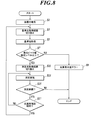
- FIG. 8 is an operation flowchart of the detection apparatus 1 when detecting an intermolecular interaction.
- the detector 10 is warmed in advance (step S1).
- the control device 50 sends a command to the microcomputer 52 so as to reach a preset temperature, and the microcomputer 52 executes temperature control of the temperature control unit 90.
- the control device 50 controls the stepping motor 82 of the switching unit 80 through the microcomputer 52 so that the incident end face of the first optical fiber 41 is shielded. Execute position switching control. Thereby, the white light of the white light source 20 can be directly guided to the spectroscope 30, and a reference light acquisition path by the third optical fiber 43 is ensured (step S3). Then, the control device 50 turns on the halogen lamp 21 of the white light source 20 through the microcomputer 52, and the white light (reference light) is received by the spectroscope 30 through the third optical fiber 43, and the spectral intensity is detected (step). S5: First detection step).
- the control device 50 receives the spectral intensity data of the reference light, and determines whether or not the light intensity in any wavelength band showing the maximum value is equal to or higher than a preset setting level (step S7). This is a process for determining whether or not the light amount has decreased due to the deterioration of the halogen lamp 21. For example, it is determined whether or not the light intensity has decreased to about 90% at the beginning of use. As a result, when the set level is not reached, the detection process is terminated and terminated as a light source emission amount error (step S9).
- the sample solution 60 including the analyte 62 is supplied from the liquid feeding unit 17 to the sealed channel 14b of the flow cell 14, and flows from the inlet 14c through the sealed channel 14b. It is distributed to the outlet 14d (see FIG. 1).
- the analyte 62 is a substance that specifically binds to the ligand 16 and is a target molecule to be detected.
- biomolecules such as proteins, nucleic acids, lipids, and sugars, and foreign substances that bind to biomolecules such as drug substances and endocrine confusion chemical substances are used.
- the control device 50 controls the stepping motor 82 of the switching unit 80 through the microcomputer 52 to position the shutter plate 81 so as to shield the incident end face of the third optical fiber 43. Execute switching control.
- the first optical fiber 41 guides the white light of the white light source 20 to the sealed flow path 14b of the flow cell 14 and irradiates it.
- the reflected light from the sealed flow path 14 b is transmitted to the spectrometer 30 by the second optical fiber 42.
- route of the measurement light by the 1st and 2nd optical fibers 41 and 42 is ensured (step S11).
- the reflected light (measurement light) is received by the spectrometer 30 through the second optical fiber 42, and the spectral intensity is detected (step S13: second detection step). Then, this spectral intensity is transmitted to the control device 50.
- the control device 50 determines whether or not to continue the measurement (step S15). If not, the process is terminated.
- the measurement time may be set in advance, and it may be determined whether or not the measurement time has elapsed, or the measurement end input is set as a setting for continuing the measurement until the measurement end input is received. The presence or absence may be determined.
- the time (light source reconfirmation time) during which the spectral intensity of white light (reference light) can change due to the influence of the temperature characteristics of the light source, aging, etc. (light source reconfirmation time) is obtained. It is determined whether time has passed (step S17).
- the light source reconfirmation time is preset in the control device 50.
- the process returns to step S13, and the measurement of the spectral intensity with respect to the reflected light (measurement light) is performed again. If the light source reconfirmation time has elapsed, the process returns to step S3, and the switching unit 80 switches to the shielded state of the first optical fiber 41, and the spectral intensity for white light (reference light) is detected again. Is done.
- the control device 50 acquires the spectral intensity data of the reference light and the spectral intensity data of the measuring light. Then, the control device 50 divides the light intensity of the measurement light by the measurement intensity of the reference light for each of the same wavelength band based on the spectral intensity of the white light (reference light) and the spectral intensity of the reflected light (measurement light). Thus, the reflectance can be calculated for each wavelength to calculate the reflection spectrum.
- the control device 50 calculates and specifies each bottom peak wavelength ⁇ bottom of the reflection spectrum before and after the binding between the analyte 62 and the ligand 16 in response to the detection result by the spectroscope 30.
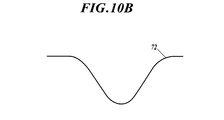
- the reflection spectrum 72 is calculated from the spectral intensity data of the reference light acquired by the measurement and the spectral intensity data of the measuring light, the waveform has an irregular shape in which minute irregularities are repeated, and the bottom peak wavelength ⁇ It is difficult to calculate and specify the bottom (FIG. 10A). Therefore, the reflection spectrum 72 is approximated by a high-order function of about 20th order, and the waveform of the reflection spectrum 72 is smoothed as shown in FIG. 10B.
- the approximation may be performed by any known method, and can be realized by, for example, the sum of a linear function and a pseudo-voig function. And the solution (minimum value) is calculated
- control device 50 periodically acquires the spectral intensity data of the reference light and the spectral intensity data of the measuring light by repeated measurement.
- the reflection spectrum is periodically calculated, the bottom peak wavelength ⁇ bottom is calculated, and the time-series change is recorded.
- white light can be transmitted from the white light source 20 to the spectroscope 30 using the third optical fiber 43 of the light transmission unit 40.
- the spectral intensity of each of the white light (reference light) and the reflected light (measurement light) is detected in a state where the influence of the temperature change and the aging of the white light source 20 is almost equal, and the control device 50 obtains the reflection spectrum. Therefore, measurement accuracy can be further improved.
- the switching unit 80 is a shutter mechanism, the shutter plate 81 is retracted from the incident end face when the respective optical fibers 41 and 43 are not shielded, so that there is nothing that attenuates the incident light, Good light transmission can be realized.
- the arrangement of the switching unit 80 described above is not limited to the white light source 20.
- the switching unit includes a reflected light receiving state that allows the reflected light of the white light from the detector 10 to be transmitted to the spectroscope 30 by the first and second optical fibers 41 and 42, and the white light by the third optical fiber 43. It is only necessary to be able to switch the white light receiving state that enables the transmission of white light from the light source 20 to the detector 10, and for this reason, in the middle of the first optical fiber 41 and the third optical fiber 43, A switching unit 80 may be provided in the middle of the second optical fiber 42 and the third optical fiber 43 or between the second optical fiber 42 and the third optical fiber 43 and the spectrometer 30.
- FIG 11 shows an example in which a switching unit 80 is provided in the middle of the first optical fiber 41 and the third optical fiber 43.
- the shutter plate 81 is disposed so as to be sandwiched between the first optical fiber 41 and the third optical fiber 43 that are divided, and between the end face of each of the optical fibers 41 and 43 and the shutter plate 81. It is sealed so that light does not enter from the gap.
- the switching unit 80 is arranged in this way, the first optical fiber 41 and the third optical fiber 43 are brought close to each other even when the housing 22 of the white light source 20 has only one connection port 23. It is possible to connect to the connection port 23 in a combined state.
- the switching unit 80 is provided in the middle of the optical fiber in this way, it is desirable to provide the housing 83 in order to prevent external light from entering from the gaps between the end faces of the optical fibers.
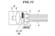
- the switching unit 80A includes a liquid crystal filter 81A disposed in the housing 22 of the white light source 20 and closely disposed on the incident end faces of the two optical fibers 41 and 43, and a drive circuit 82A.
- the liquid crystal filter has two shielding areas that cover the incident end face of the first optical fiber 41 and the incident end face of the third optical fiber 43. The light transmission state and the shielding state of each shielding area are determined by the drive circuit 82A. It is possible to switch according to the operation signal.
- the drive circuit 82A is configured to switch and drive the liquid crystal filter 81A under the control of the microcomputer 52.
- the liquid crystal filter 81A When the liquid crystal filter 81A is used, the moving operation of the member can be made unnecessary, so that a gap due to the operation is not easily generated, and high light shielding performance can be realized. Therefore, the two optical fibers 41 and 43 can be arranged closer to each other, and the switching unit 80A can be downsized. Further, it can be arbitrarily manufactured in the shape of the light shielding area, and even when the fine fibers constituting the respective optical fibers 41 and 43 are combined with each other as in the example of FIG. It is possible to form a shielding area corresponding to the distribution of each fine fiber.
- the switching unit 80A using the liquid crystal filter 81A is also in the middle of the first optical fiber 41 and the third optical fiber 43, in the middle of the second optical fiber 42 and the third optical fiber 43, or in the second optical fiber.
- a switching unit 80 may be provided between the optical fiber 42 and the third optical fiber 43 and the spectrometer 30.
- FIG. 13 shows an example in which a switching unit 80 ⁇ / b> A is provided in the middle of the first optical fiber 41 and the third optical fiber 43.
- the liquid crystal filter 81A is disposed so as to be sandwiched between the divided first optical fiber 41 and third optical fiber 43, and between the end face of each optical fiber 41, 43 and the liquid crystal filter 81A. The entry of light from the gap is sealed to the contents. Also in this case, it is desirable to provide the housing 83A in order to prevent external light from entering from the gaps between the end faces of the optical fibers.
- connection method is not limited to this.
- the connection method is not limited to this.
- light from one optical fiber 43 (or 42) may be transmitted straight to the spectroscope 30 and transmitted to the other optical fiber.
- the optical fibers 42 and 43 may be connected so that light from 42 (or 43) may be guided to the spectroscope 30 by being reflected by the reflecting surface.
- the second optical fiber 42 and the third optical fiber 43 receive light at different portions of the light receiving surface of the spectrometer 30.
- the optical fibers 42 and 43 can also receive light at the same portion of the light receiving surface of the spectrometer 30 and can make the detection state uniform.
Landscapes
- Physics & Mathematics (AREA)
- Chemical & Material Sciences (AREA)
- General Health & Medical Sciences (AREA)
- Health & Medical Sciences (AREA)
- Life Sciences & Earth Sciences (AREA)
- Analytical Chemistry (AREA)
- Biochemistry (AREA)
- General Physics & Mathematics (AREA)
- Immunology (AREA)
- Pathology (AREA)
- Chemical Kinetics & Catalysis (AREA)
- Plasma & Fusion (AREA)
- Engineering & Computer Science (AREA)
- Investigating Or Analysing Materials By Optical Means (AREA)
- Optical Measuring Cells (AREA)
Abstract
Description
しかしながら、そのような予め用意された波長分布特性の基準データは、試験体検出時における光源の温度特性や経年劣化に対する光源強度の波長分布特性は加味されてはいないことから、当該基準データを用いて反射光の反射スペクトルを求めると光源の温度特性や経年劣化等の影響により、検出精度が低下すると言う問題が生じていた。
リガンドを有する検出器と、
白色光の発光を行う白色光源と、
受光する光の分光強度を検出する分光器と、
前記白色光源から前記検出器に白色光を伝達する第一の光伝達経路と、前記検出器から前記分光器に前記白色光の反射光を伝達する第二の光伝達経路と、前記白色光源から前記分光器に白色光を伝達する第三の光伝達経路とを有する光伝達部と、
前記第一及び第二の光伝達経路による前記検出器での白色光の反射光の前記分光器への伝達を可能とする反射光受光状態と、前記第三の光伝達経路による前記白色光源から前記検出器への白色光の伝達を可能とする白色光受光状態とを切り換える切り換え部と、
前記切り換え部と前記分光器とを制御して、前記白色光受光状態と前記反射光受光状態のそれぞれにおいて分光強度を検出する制御を行う制御部とを備えることを特徴とする分子間相互作用の検出装置が提供される。
さらに、前記検出装置の切り換え部は、位置切り換えが行われる遮蔽体により、前記第一の光伝達経路による光伝達の遮蔽状態と、前記二又は第三の光伝達経路による光伝達の遮蔽状態とを選択的に切り換え可能なシャッター機構とすることができる。
或いは、前記検出装置の切り換え部は、前記第一の光伝達経路による光伝達の遮蔽状態と、前記二又は第三の光伝達経路による光伝達の遮蔽状態とを選択的に切り換え可能な液晶フィルタとすることができる。
リガンドを有する検出器と、白色光の発光を行う白色光源と、受光する光の分光強度を検出する分光器と、前記白色光源から前記検出器に白色光を伝達する第一の光伝達経路と前記検出器から前記分光器に前記白色光の反射光を伝達する第二の光伝達経路と前記白色光源から前記分光器に白色光を伝達する第三の光伝達経路とを有する光伝達部とを備える検出装置を用いて分子間相互作用の検出を行う検出方法であって、
前記第一及び第二の光伝達経路により前記検出器での白色光の反射光を受光してその分光強度を前記分光器で検出する第1の検出工程と、
前記第1の検出工程に前後して、前記第三の光伝達経路により前記白色光源からの白色光を受光してその分光強度を前記分光器で検出する第2の検出工程と、
前記第1の検出工程と前記第2の検出工程によって得られた前記白色光の分光強度と前記反射光の分光強度とに基づいて、一定の波長間隔ごとの反射率を算出して反射スペクトルを求める算出工程とを備えることを特徴とする分子間相互作用の検出方法が提供される。
また、切り換えを行う二つの光伝達経路を離間して配置しなくとも、それぞれの光伝達経路の切り換えを実現することが可能である。
以下、図面を参照しながら本発明の好ましい実施形態について説明する。図1は本発明の実施形態である分子間相互作用の検出装置1の構成を簡略的に図示した模式図、図2Aは装置の上枠及びカバーを外して内部構成を見える状態とした検出装置1の右側面図、図2Bは左側面図、図3は検出装置1の機能ブロック図である。
図1乃至図3に示すように、検出装置1は、主に、検出器10,白色光源20,分光器30,光伝達部40,切り換え部80,温度制御部90,制御装置50などから構成されている。
図4に示すとおり、センサーチップ12は矩形状を呈したシリコン基板12aを有している。シリコン基板12a上にはSiN膜12b(窒化シリコン)が蒸着されている。SiN膜12bは光学薄膜の一例である。
フローセル14はシリコーンゴム製の透明な部材である。フローセル14には溝14aが形成されている。フローセル14をセンサーチップ12に密着させると、密閉流路14bが形成される(図1参照)。溝14aの両端部はフローセル14の表面から露出しており、一方の端部が送液部17に接続されてサンプル溶液が供給される流入口14cとして機能し、他方の端部は廃液部18に接続されてサンプル溶液の流出口14dとして機能するようになっている。
また、フローセル14の溝14aの底部にはリガンド16が結合されている(図1参照)。
第一の光ファイバ41は、白色光源20から発せられた白色光をフローセル14まで導くためのものであり、白色光源20が点灯すると、その白色光が第一の光ファイバ41を介して密閉流路14bを照射する。
第二の光ファイバ42は、フローセル14から分光器30に光を導くためのものであり、白色光源20の白色光が密閉流路14bを照射した時の反射光を分光器30に導いて検出することを可能としている。
なお、上記「白色光を直接分光器30に導く」とは、白色光源20からの白色光がいずれかを経由して反射を行うことなく分光器30まで導くことを意味する(光ファイバの内部反射は除く)。
上記各光ファイバ41~43は、いずれも微細ファイバを束ねた構造となっている。
そして、第一の光ファイバ41と第二の光ファイバ42のフローセル14側の端部は、図5に示すように、各々の微細ファイバが一つの束となるように複合的に寄り合わされている。即ち、第一の光ファイバ41を構成する微細ファイバ41aは、フローセル14側の端面において中央に分布し、第二の光ファイバ42を構成する微細ファイバ42aは第一の光ファイバ41の微細ファイバの束を取り囲むようにその周囲に分布している。なお、図5ではそれぞれの微細ファイバ41a,42aを識別できるように第一の光ファイバ41の微細ファイバのみ色彩を付して図示しているが実際にはいずれの微細ファイバ41a,42aとも無色透明である。
この分光器30は、受光部で受光する光に含まれる一定の波長間隔ごとの光について光強度を検出し、分光強度として制御装置50に出力する。
白色光源20は、ハロゲンランプ21と、これを格納する筐体22とから構成されている。筐体22には、前述したように、第一の光ファイバ41と第三の光ファイバ43とをそれぞれ接続するための接続ポート23,24が設けられている。
各接続ポート23,24に接続された各光ファイバ41,43はいずれもそれぞれの光入射端面がハロゲンランプ21に対向するように配置されており、ハロゲンランプ21と各光ファイバ41,43との間には、切り換え部80が設けられている。
シャッター板81は、遮光性の高い素材からなる平板であり、上記二位置間を移動可能となるように図示しないガイド機構により保持されている。また、このシャッター板81は、各光ファイバ41,43の入射端面を遮蔽する際に隙間を生じないようシールが施されており、密閉性を高めている。
また、ステッピングモータ42とシャッター板81との間には、ステッピングモータ42の回転駆動を直動動作に変換する図示しない変換機構が設けられている。
なお、切り換え部80の駆動源はステッピングモータ42に限らず動作の制御が可能な他の種類のモータでも良いし、直動動作を行うエアシリンダやソレノイド等のアクチュエータでも良い。
切り換え部80により、第三の光ファイバ43の入射端面が遮蔽状態の時には、第一の光ファイバ41を通じてフローセル14の密閉流路14bに白色光を照射することができ、さらに、その反射光を第二の光ファイバ42を通じて分光器30に伝達し、その分光強度を検出することができる。
また、切り換え部80により、第一の光ファイバ41の入射端面が遮蔽状態の時には、
第一の光ファイバ41を通じて分光器30に白色光を伝達することができ、その分光強度を検出することができる。
また、制御装置50は、分光器30から基準となる白色光の分光強度や測定に基づく反射光の分光強度の検出データを受信し、これらに基づいて各波長帯域ごとの反射率を算出し、反射スペクトルを算出する。これにより、制御装置50は、算出部として機能する。
マイコン52は、制御装置50の制御指令に応じて白色光源20の点灯と消灯を切り換える制御を行ったり、制御装置50の設定温度指令に応じて温度制御部90の温度制御を行ったり、制御装置50の制御指令に応じて切り換え部80のシャッター板81の位置切り換え動作制御を実行する。
次に、検出装置1を用いた分子間相互作用の検出方法について図8~10に基づいて説明する。図8は分子間相互作用の検出時の検出装置1の動作フローチャートである。
検出を行う際には予め検出器10の暖気が行われる(ステップS1)。即ち、制御装置50は、予め定めた設定温度となるようマイコン52に指令を送り、マイコン52は温度制御部90の温度制御を実行する。
そして、制御装置50はマイコン52を通じて、白色光源20のハロゲンランプ21を点灯させ、第三の光ファイバ43を通じて白色光(基準光)が分光器30に受光され、分光強度が検出される(ステップS5:第一の検出工程)。
その結果、設定レベルに満たない時には、光源発光量エラーとして、検出処理を中止して終了する(ステップS9)。
次いで、第二の光ファイバ42を通じて反射光(測定光)が分光器30に受光され、分光強度が検出される(ステップS13:第二の検出工程)。そして、この分光強度は制御装置50に送信される。
また、光源再確認時間が経過した場合には、ステップS3に処理を戻し、切り換え部80によって第一の光ファイバ41の遮蔽状態に切り換えられ、白色光(基準光)についての分光強度が再び検出される。
そして、制御装置50は、白色光(基準光)の分光強度と反射光(測定光)の分光強度とにより、同一の波長帯域ごとに測定光の光強度を基準光の測定強度で除算することで各波長ごとに反射率を求めて反射スペクトルを算出することができる。
制御装置50では、分光器30による検出結果を受けてアナライト62とリガンド16との結合前後での反射スペクトルの各ボトムピーク波長λbottomを算出・特定する。
従って、反射スペクトル72を20次程度の高次関数で近似し、図10Bに示すとおり、反射スペクトル72の波形を滑らかにする。当該近似は公知のいずれの手法によるものであってもよく、例えば線形の関数と擬似voigt関数の和で実現することができる。
そして、かかる高次多項式からその解(最小値)を求めて、これをボトムピーク値として特定する。
以上のように、分子間相互作用の検出装置1では、光伝達部40の第三の光ファイバ43を用いて白色光源20から分光器30に白色光を伝達することができるので、検出器10の反射光から分光強度を検出する際に、時を隔てることなく、基準となる白色光の分光強度も検出することができる。これにより、白色光源20の温度変化や経年劣化の影響がほぼ等しい状態で白色光(基準光)と反射光(測定光)のそれぞれの分光強度を検出し、制御装置50において、反射スペクトルを求めることができるため、計測精度をより向上させることが可能となる。
前述した切り換え部80の配置は白色光源20に限定されるものではない。切り換え部は、第一及び第二の光ファイバ41,42による検出器10での白色光の反射光の分光器30への伝達を可能とする反射光受光状態と第三の光ファイバ43による白色光源20から検出器10への白色光の伝達を可能とする白色光受光状態とを切り換えることが可能であればよく、このため、第一の光ファイバ41及び第三の光ファイバ43の途中、第二の光ファイバ42及び第三の光ファイバ43の途中又は第二の光ファイバ42及び第三の光ファイバ43と分光器30との間に切り換え部80を設けても良い。
図11は、第一の光ファイバ41及び第三の光ファイバ43の途中に切り換え部80を設けた例を示している。この場合、分割された第一の光ファイバ41及び第三の光ファイバ43の間にシャッター板81が挟み込まれるように配置され、各光ファイバ41,43の端面とシャッター板81との間には隙間からの光の侵入が生じないようにシールされている。
切り換え部80をこのように配置する場合、白色光源20の筐体22に接続ポート23が一つしか設けられていない場合でも、第一の光ファイバ41と第三の光ファイバ43を寄り合わせて結合させた状態で接続ポート23に接続することが可能となる。なお、このように光ファイバの途中に切り換え部80を設ける場合には、各光ファイバの端面の隙間からの外部の光の侵入を防止するために筐体83を設けることが望ましい。
また、シャッター機構を利用する切り換え部80に限らず、図12に示すような液晶フィルタ81Aを利用した切り換え部80Aを利用しても良い。
この切り換え部80Aは、白色光源20の筐体22内に配置され、二つの光ファイバ41,43の入射端面に密接配置した液晶フィルタ81Aとその駆動回路82Aとを備えている。液晶フィルタは、第一の光ファイバ41の入射端面と第三の光ファイバ43の入射端面とを覆う二つの遮蔽エリアを有し、各遮蔽エリアの光透過状態と遮蔽状態とを駆動回路82Aの動作信号に応じて切り換えることが可能となっている。また、駆動回路82Aは、マイコン52の制御の下で、液晶フィルタ81Aの切り換え駆動を行うようになっている。
液晶フィルタ81Aを利用する場合、部材の移動動作を不要とすることができるので、動作による隙間などが生じにくく、高い遮光性を実現することができる。従って、二つの光ファイバ41,43をより近接配置することが可能となり、切り換え部80Aの小型化を図ることが可能となる。また、遮光するエリアの形状に任意に製造することができ、図5の例のようにそれぞれの光ファイバ41,43を構成する微細ファイバを複合的に寄り合わされた場合でも、光ファイバ41,43それぞれの微細ファイバの分布に応じた遮蔽エリアを形成することが可能である。
図13は第一の光ファイバ41及び第三の光ファイバ43の途中に切り換え部80Aを設けた例を示している。この場合、分割された第一の光ファイバ41及び第三の光ファイバ43の間に液晶フィルタ81Aが挟み込まれるように配置され、各光ファイバ41,43の端面と液晶フィルタ81Aとの間には隙間からの光の侵入が内容にシールされている。また、この場合も、各光ファイバの端面の隙間からの外部の光の侵入を防止するために筐体83Aを設けることが望ましい。
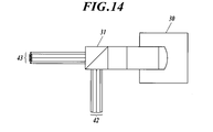
前述した図6の例では、第二の光ファイバ42と第三の光ファイバ43とを寄り合わせて同時に分光器30に接続したが、接続方法としてはこれに限るものではない。
例えば、図14に示すように、内部に反射面を有するプリズム31を利用して、一方の光ファイバ43(42でも良い)からの光を直進透過可能として分光器30に導き、他方の光ファイバ42(43でも良い)からの光を反射面で反射させることで分光器30に導くように各光ファイバ42,43を接続しても良い。図6の例では、第二の光ファイバ42と第三の光ファイバ43とが分光器30の受光面における異なる部分に光が受光することとなるが、上記プリズムを利用する場合には、いずれの光ファイバ42,43も分光器30の受光面における同一部分に光を受光させることができ、検出状態の均一化を図ることを可能とする。
10 検出器
12 センサーチップ
14 フローセル
16 リガンド
20 白色光源
30 分光器
40 光伝達部
41 第一の光ファイバ(第一の光伝達経路)
42 第二の光ファイバ(第二の光伝達経路)
43 第三の光ファイバ(第三の光伝達経路)
50 制御装置(制御部、算出部)
60 サンプル溶液
62 アナライト
72 反射スペクトル
80,80A 切り換え部
81 シャッター板(遮蔽体)
81A 液晶フィルタ
Claims (5)
- リガンドを有する検出器と、
白色光の発光を行う白色光源と、
受光する光の分光強度を検出する分光器と、
前記白色光源から前記検出器に白色光を伝達する第一の光伝達経路と、前記検出器から前記分光器に前記白色光の反射光を伝達する第二の光伝達経路と、前記白色光源から前記分光器に白色光を伝達する第三の光伝達経路とを有する光伝達部と、
前記第一及び第二の光伝達経路による前記検出器での白色光の反射光の前記分光器への伝達を可能とする反射光受光状態と、前記第三の光伝達経路による前記白色光源から前記検出器への白色光の伝達を可能とする白色光受光状態とを切り換える切り換え部と、
前記切り換え部と前記分光器とを制御して、前記白色光受光状態と前記反射光受光状態のそれぞれにおいて分光強度を検出する制御を行う制御部とを備えることを特徴とする分子間相互作用の検出装置。 - 前記制御部の制御によって得られた前記白色光の分光強度と前記反射光の分光強度とに基づいて、一定の波長間隔ごとの反射率を算出して反射スペクトルを求める算出部を備えることを特徴とする分子間相互作用の検出装置。
- 前記切り換え部は、位置切り換えが行われる遮蔽体により、前記第一の光伝達経路による光伝達の遮蔽状態と、前記二又は第三の光伝達経路による光伝達の遮蔽状態とを選択的に切り換え可能なシャッター機構であることを特徴とする請求項1又は2記載の分子間相互作用の検出装置。
- 前記切り換え部は、前記第一の光伝達経路による光伝達の遮蔽状態と、前記二又は第三の光伝達経路による光伝達の遮蔽状態とを選択的に切り換え可能な液晶フィルタであることを特徴とする請求項1又は2記載の分子間相互作用の検出装置。
- リガンドを有する検出器と、白色光の発光を行う白色光源と、受光する光の分光強度を検出する分光器と、前記白色光源から前記検出器に白色光を伝達する第一の光伝達経路と前記検出器から前記分光器に前記白色光の反射光を伝達する第二の光伝達経路と前記白色光源から前記分光器に白色光を伝達する第三の光伝達経路とを有する光伝達部とを備える検出装置を用いて分子間相互作用の検出を行う検出方法であって、
前記第一及び第二の光伝達経路により前記検出器での白色光の反射光を受光してその分光強度を前記分光器で検出する第1の検出工程と、
前記第1の検出工程に前後して、前記第三の光伝達経路により前記白色光源からの白色光を受光してその分光強度を前記分光器で検出する第2の検出工程と、
前記第1の検出工程と前記第2の検出工程によって得られた前記白色光の分光強度と前記反射光の分光強度とに基づいて、一定の波長間隔ごとの反射率を算出して反射スペクトルを求める算出工程とを備えることを特徴とする分子間相互作用の検出方法。
Priority Applications (4)
| Application Number | Priority Date | Filing Date | Title |
|---|---|---|---|
| US13/812,353 US8681338B2 (en) | 2010-07-27 | 2011-05-18 | Detection device and detection method for intermolecular interaction |
| JP2012526356A JPWO2012014551A1 (ja) | 2010-07-27 | 2011-05-18 | 分子間相互作用の検出装置及び検出方法 |
| EP11812146.6A EP2600138A4 (en) | 2010-07-27 | 2011-05-18 | DETECTION DEVICE AND DETECTION METHOD FOR INTERMOLECULAR INTERACTION |
| CN201180036406XA CN103026203A (zh) | 2010-07-27 | 2011-05-18 | 分子间相互作用的检测装置及检测方法 |
Applications Claiming Priority (2)
| Application Number | Priority Date | Filing Date | Title |
|---|---|---|---|
| JP2010167835 | 2010-07-27 | ||
| JP2010-167835 | 2010-07-27 |
Publications (1)
| Publication Number | Publication Date |
|---|---|
| WO2012014551A1 true WO2012014551A1 (ja) | 2012-02-02 |
Family
ID=45529774
Family Applications (1)
| Application Number | Title | Priority Date | Filing Date |
|---|---|---|---|
| PCT/JP2011/061369 WO2012014551A1 (ja) | 2010-07-27 | 2011-05-18 | 分子間相互作用の検出装置及び検出方法 |
Country Status (5)
| Country | Link |
|---|---|
| US (1) | US8681338B2 (ja) |
| EP (1) | EP2600138A4 (ja) |
| JP (1) | JPWO2012014551A1 (ja) |
| CN (1) | CN103026203A (ja) |
| WO (1) | WO2012014551A1 (ja) |
Cited By (1)
| Publication number | Priority date | Publication date | Assignee | Title |
|---|---|---|---|---|
| CN108303387A (zh) * | 2017-01-11 | 2018-07-20 | 罗伯特·博世有限公司 | 用于分析测量区域的方法和微型光谱仪 |
Families Citing this family (6)
| Publication number | Priority date | Publication date | Assignee | Title |
|---|---|---|---|---|
| US10451548B2 (en) * | 2016-01-15 | 2019-10-22 | The Mitre Corporation | Active hyperspectral imaging system |
| CN105891466A (zh) * | 2016-04-26 | 2016-08-24 | 中国科学技术大学 | 一种检测生物分子的装置及方法 |
| CN108344714B (zh) * | 2018-01-16 | 2020-07-31 | 东南大学 | 基于有序多孔纳米结构薄膜干涉效应的生物检测仪及其进行生物分子检测的方法 |
| US10983044B2 (en) * | 2018-06-26 | 2021-04-20 | Arometrix, Inc. | Device, system and method for in-situ optical monitoring and control of extraction and purification of plant materials |
| WO2020135957A1 (en) * | 2018-12-27 | 2020-07-02 | ams Sensors Germany GmbH | Compensation of temperature effects in a sensor system |
| EP4271981A1 (en) * | 2020-12-30 | 2023-11-08 | Seegene, Inc. | Optical spectrometry-based method and device for detecting target analyte in sample |
Citations (6)
| Publication number | Priority date | Publication date | Assignee | Title |
|---|---|---|---|---|
| JPS63200026A (ja) * | 1987-02-16 | 1988-08-18 | Sumitomo Electric Ind Ltd | 赤外分光分析器 |
| JPH1183628A (ja) * | 1997-09-02 | 1999-03-26 | Omron Corp | 土壌の光学特性測定装置 |
| JPH11160317A (ja) * | 1997-11-27 | 1999-06-18 | Suzuki Motor Corp | 免疫反応測定装置 |
| JP2004132799A (ja) * | 2002-10-10 | 2004-04-30 | Hitachi Ltd | 生化学センサ用キットおよび測定装置 |
| JP2005321349A (ja) * | 2004-05-11 | 2005-11-17 | Ishikawajima Harima Heavy Ind Co Ltd | 材質判断装置 |
| JP2009507569A (ja) * | 2005-09-13 | 2009-02-26 | エドワーズ ライフサイエンシーズ コーポレイション | 総ヘモグロビンの継続的な分光測定 |
Family Cites Families (8)
| Publication number | Priority date | Publication date | Assignee | Title |
|---|---|---|---|---|
| US5804453A (en) * | 1996-02-09 | 1998-09-08 | Duan-Jun Chen | Fiber optic direct-sensing bioprobe using a phase-tracking approach |
| US6139797A (en) * | 1997-08-20 | 2000-10-31 | Suzuki Motor Corporation | Immunoassay apparatus |
| US6512577B1 (en) * | 2000-03-13 | 2003-01-28 | Richard M. Ozanich | Apparatus and method for measuring and correlating characteristics of fruit with visible/near infra-red spectrum |
| US7507579B2 (en) * | 2002-05-01 | 2009-03-24 | Massachusetts Institute Of Technology | Apparatus and methods for simultaneous operation of miniaturized reactors |
| EP1508031B1 (en) * | 2002-05-28 | 2009-05-06 | FOSS Analytical A/S | A method and a spectrometer for quantitative determination of a constituent in a sample |
| US7319525B2 (en) * | 2003-11-06 | 2008-01-15 | Fortebio, Inc. | Fiber-optic assay apparatus based on phase-shift interferometry |
| WO2007008151A1 (en) * | 2005-07-08 | 2007-01-18 | Portendo Ab | Sensor structures, methods of manufacturing them and detectors including sensor structures |
| US20080108122A1 (en) * | 2006-09-01 | 2008-05-08 | State of Oregon acting by and through the State Board of Higher Education on behalf of Oregon | Microchemical nanofactories |
-
2011
- 2011-05-18 EP EP11812146.6A patent/EP2600138A4/en not_active Withdrawn
- 2011-05-18 US US13/812,353 patent/US8681338B2/en not_active Expired - Fee Related
- 2011-05-18 WO PCT/JP2011/061369 patent/WO2012014551A1/ja active Application Filing
- 2011-05-18 CN CN201180036406XA patent/CN103026203A/zh active Pending
- 2011-05-18 JP JP2012526356A patent/JPWO2012014551A1/ja active Pending
Patent Citations (7)
| Publication number | Priority date | Publication date | Assignee | Title |
|---|---|---|---|---|
| JPS63200026A (ja) * | 1987-02-16 | 1988-08-18 | Sumitomo Electric Ind Ltd | 赤外分光分析器 |
| JPH1183628A (ja) * | 1997-09-02 | 1999-03-26 | Omron Corp | 土壌の光学特性測定装置 |
| JPH11160317A (ja) * | 1997-11-27 | 1999-06-18 | Suzuki Motor Corp | 免疫反応測定装置 |
| JP2004132799A (ja) * | 2002-10-10 | 2004-04-30 | Hitachi Ltd | 生化学センサ用キットおよび測定装置 |
| JP3786073B2 (ja) | 2002-10-10 | 2006-06-14 | 株式会社日立製作所 | 生化学センサ用キットおよび測定装置 |
| JP2005321349A (ja) * | 2004-05-11 | 2005-11-17 | Ishikawajima Harima Heavy Ind Co Ltd | 材質判断装置 |
| JP2009507569A (ja) * | 2005-09-13 | 2009-02-26 | エドワーズ ライフサイエンシーズ コーポレイション | 総ヘモグロビンの継続的な分光測定 |
Non-Patent Citations (2)
| Title |
|---|
| SANDSTROM ET AL., APPL. OPT., vol. 24, 1985, pages 472 |
| See also references of EP2600138A4 |
Cited By (2)
| Publication number | Priority date | Publication date | Assignee | Title |
|---|---|---|---|---|
| CN108303387A (zh) * | 2017-01-11 | 2018-07-20 | 罗伯特·博世有限公司 | 用于分析测量区域的方法和微型光谱仪 |
| CN108303387B (zh) * | 2017-01-11 | 2022-03-15 | 罗伯特·博世有限公司 | 用于分析测量区域的方法和微型光谱仪 |
Also Published As
| Publication number | Publication date |
|---|---|
| EP2600138A1 (en) | 2013-06-05 |
| JPWO2012014551A1 (ja) | 2013-09-12 |
| EP2600138A4 (en) | 2015-07-08 |
| CN103026203A (zh) | 2013-04-03 |
| US20130122607A1 (en) | 2013-05-16 |
| US8681338B2 (en) | 2014-03-25 |
Similar Documents
| Publication | Publication Date | Title |
|---|---|---|
| WO2012014551A1 (ja) | 分子間相互作用の検出装置及び検出方法 | |
| JP5704163B2 (ja) | 分子間相互作用の検出方法およびその検出装置 | |
| CN111742212B (zh) | 流体检测面板和流体检测装置 | |
| JP6536413B2 (ja) | 表面プラズモン共鳴蛍光分析装置および表面プラズモン共鳴蛍光分析方法 | |
| US20130267034A1 (en) | Intermolecular interaction measurement method, measurement system for use in the method, and program | |
| WO2012108323A1 (ja) | 表面プラズモン励起蛍光計測装置及び表面プラズモン励起蛍光計測方法 | |
| EP3321688B1 (en) | Detection device and detection method | |
| JP6760384B2 (ja) | 測定方法 | |
| JPH0815131A (ja) | 劣化診断システム | |
| EP1064095A1 (en) | Method and apparatus for measuring proteins | |
| JP4173746B2 (ja) | 測定装置 | |
| JP4173725B2 (ja) | エバネッセント波を利用したセンサー | |
| US20020131897A1 (en) | Apparatus of handling fluids | |
| JP5640873B2 (ja) | 表面プラズモン励起蛍光計測装置及び表面プラズモン励起蛍光計測方法 | |
| WO2012096037A1 (ja) | 分子間相互作用の検出方法及びこれに使用されるキット | |
| WO2018135503A1 (ja) | 光学式検体検出システムにおけるセンサーチップの位置検出方法及び位置検出装置 | |
| JP2012150076A (ja) | 分子間相互作用の測定システム、分子間相互作用の測定プログラム、及び、分子間相互作用の測定方法 | |
| WO2016098653A1 (ja) | 検出方法および検出装置 | |
| JP2014106215A (ja) | センサーチップ及び測定装置 | |
| JP2012127712A (ja) | 分子間相互作用の測定装置 | |
| JP2012137467A (ja) | 分子間相互作用の測定装置 | |
| US20190162722A1 (en) | Detection Apparatus and Detection Method | |
| JPH05107181A (ja) | 近赤外線分光分析装置における検出部 |
Legal Events
| Date | Code | Title | Description |
|---|---|---|---|
| WWE | Wipo information: entry into national phase |
Ref document number: 201180036406.X Country of ref document: CN |
|
| 121 | Ep: the epo has been informed by wipo that ep was designated in this application |
Ref document number: 11812146 Country of ref document: EP Kind code of ref document: A1 |
|
| WWE | Wipo information: entry into national phase |
Ref document number: 2012526356 Country of ref document: JP |
|
| REEP | Request for entry into the european phase |
Ref document number: 2011812146 Country of ref document: EP |
|
| WWE | Wipo information: entry into national phase |
Ref document number: 2011812146 Country of ref document: EP |
|
| WWE | Wipo information: entry into national phase |
Ref document number: 13812353 Country of ref document: US |
|
| NENP | Non-entry into the national phase |
Ref country code: DE |