WO2012014493A1 - 結合配線および回路装置 - Google Patents
結合配線および回路装置 Download PDFInfo
- Publication number
- WO2012014493A1 WO2012014493A1 PCT/JP2011/004316 JP2011004316W WO2012014493A1 WO 2012014493 A1 WO2012014493 A1 WO 2012014493A1 JP 2011004316 W JP2011004316 W JP 2011004316W WO 2012014493 A1 WO2012014493 A1 WO 2012014493A1
- Authority
- WO
- WIPO (PCT)
- Prior art keywords
- conductor
- signal line
- line conductor
- ground
- dielectric layer
- Prior art date
- Legal status (The legal status is an assumption and is not a legal conclusion. Google has not performed a legal analysis and makes no representation as to the accuracy of the status listed.)
- Ceased
Links
Images




Classifications
-
- H—ELECTRICITY
- H01—ELECTRIC ELEMENTS
- H01P—WAVEGUIDES; RESONATORS, LINES, OR OTHER DEVICES OF THE WAVEGUIDE TYPE
- H01P3/00—Waveguides; Transmission lines of the waveguide type
- H01P3/02—Waveguides; Transmission lines of the waveguide type with two longitudinal conductors
- H01P3/08—Microstrips; Strip lines
Definitions
- the present invention relates to a coupling wiring having a coupling line used for transmission of a high-frequency signal and a circuit device including the coupling wiring.
- a coupling wiring including a pair of signal line conductors electromagnetically coupled to each other is known.
- a configuration in which the intermediate conductor is grounded separately from the signal line conductor is used (see Patent Document 1).
- the present invention has been made in view of such problems, and an object of the present invention is to provide a technique capable of improving the odd-mode characteristics while suppressing the influence on the even-mode characteristics in the coupled line.
- An aspect of the present invention is a combined wiring.
- the coupling wiring is provided between the first ground conductor, the second ground conductor provided opposite to the first ground conductor, and the first ground conductor and the second ground conductor.
- a dielectric layer, a first signal line conductor and a second signal line conductor, which are embedded in the dielectric layer so as to be spaced apart from each other and electromagnetically coupled to each other, and the first signal line conductor and the second signal line conductor In the cross section perpendicular to the signal transmission direction of the first signal line conductor and the second signal line conductor.
- the intermediate conductor is located in a region where the first signal line conductor and the second signal line conductor overlap.
- the width of the intermediate conductor is Wf
- the length of the first signal line conductor and the second signal line conductor is overlapped is Wc
- the first signal line conductor and the second signal are overlapped.
- the thickness of the line conductor is t
- at least one resonator connected to the intermediate conductor and resonating at a predetermined frequency may be further provided.
- the circuit device includes the coupling wiring according to any one of the aspects described above, wherein one end of the first signal line conductor and the other end of the second signal line conductor are input / output ends, The other end and one end of the second signal line conductor are grounded.
- the odd-mode characteristics can be improved while suppressing the influence on the even-mode characteristics in the coupled line.
- FIG. 3 is a cross-sectional view orthogonal to the signal transmission direction of the coupled wiring according to Embodiment 1.
- FIG. 2 is a cross-sectional view taken along line A-A ′ of FIG. 1 and shows a cross section along the signal transmission direction of the coupled wiring according to the first embodiment.
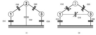
- FIGS. 3A and 3B are equivalent circuit diagrams for the even mode and the odd mode of the coupled wiring according to the first embodiment, respectively. It is a graph which shows the relationship between the width Wf of an intermediate
- 6 is a cross-sectional view of a circuit device according to a second embodiment along a signal transmission direction.
- FIG. 1 is a cross-sectional view taken along line A-A ′ of FIG. 1 and shows a cross section along the signal transmission direction of the coupled wiring according to the first embodiment.
- FIGS. 3A and 3B are equivalent circuit diagrams for the even mode and the odd mode of the coupled wiring according to the first embodiment,
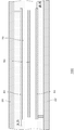
- FIG. 10 is a perspective view showing an arrangement of resonators in a circuit device according to Embodiment 3.
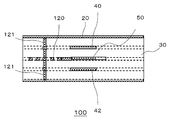
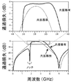
- FIG. 7 is a cross-sectional view taken along line B-B ′ in FIG. 6. It is an enlarged view of the resonator shown in FIG. It is a graph which shows a passage loss when the circuit device concerning Embodiments 2 and 3 is used as a transmission line.
- FIG. 1 is a cross-sectional view orthogonal to the signal transmission direction of the coupled wiring 10 according to the first embodiment.
- FIG. 2 is a cross-sectional view taken along line AA ′ in FIG. 1, and shows a cross section along the signal transmission direction of the coupled wiring according to the first embodiment.
- the coupling wiring 10 includes a first ground conductor 20, a second ground conductor 22, a dielectric layer 30, a first signal line conductor 40, a second signal line conductor 42, and an intermediate conductor 50.
- the first ground conductor 20 and the second ground conductor 22 are strip-shaped conductors provided so as to face each other, and are both grounded.
- the dielectric layer 30 is provided between the first ground conductor 20 and the second ground conductor 22 and is formed of, for example, an epoxy resin.
- the first signal line conductor 40 and the second signal line conductor 42 are connected to the dielectric layer 30 between the first ground conductor 20 and the second ground conductor 22.
- the conductor 22 is buried in parallel.
- the first signal line conductor 40 and the second signal line conductor 42 are strip-shaped conductors provided to face each other, and are electromagnetically coupled to each other. In the present embodiment, the case where the width of the first signal line conductor 40 and the width of the second signal line conductor 42 are the same is shown.
- the intermediate conductor 50 is a strip-shaped conductor embedded in the dielectric layer 30 between the first signal line conductor 40 and the second signal line conductor 42, and the potential thereof is a floating potential.
- the width Wf of the intermediate conductor 50 is such that the first signal line conductor 40 and the second signal line conductor 42 are the same. It is shorter than the overlapping length. More preferably, the width Wf of the intermediate conductor 50 is defined as Wc in which the first signal line conductor 40 and the second signal line conductor 42 overlap each other, and the intermediate conductor 50, the first signal line conductor 40, and the first signal line conductor 40 When the thickness of the second signal line conductor 42 is t, it is preferable to satisfy the relationship 0 ⁇ Wf ⁇ Wc ⁇ t.
- FIGS. 3A and 3B show equivalent circuit diagrams of the even mode and the odd mode when the intermediate conductor 50 is used.
- the circled numbers 1, 2, and 3 correspond to the first signal line conductor 40, the intermediate conductor 50, and the second signal line conductor 42, respectively.
- the capacitance C11 between the first signal line conductor 40 and the ground potential is smaller than the capacitance C33 between the second signal line conductor 42 and the ground potential.
- the capacity C22 is negligible.
- the impedance is fixed by C11 + C33. Therefore, in the even mode, the impedance is determined without depending on the width Wf of the intermediate conductor 50.
- the capacitance between the first signal line conductor 40 and the intermediate conductor 50 in addition to the capacitance C13 between the first signal line conductor 40 and the second signal line conductor 42 is adjusted by the capacitance C23 between C12 and the intermediate conductor 50 and the second signal line conductor 42.
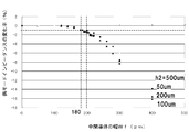
- FIG. 4 is a graph showing the relationship between the width Wf of the intermediate conductor and the even-mode impedance change rate.
- the horizontal axis of FIG. 4 indicates the width of the intermediate conductor, and the vertical axis of FIG. 4 indicates the rate of change of the even-mode impedance in the coupled wiring at the width of each intermediate conductor when there is no intermediate conductor.
- the dimensions of the coupled wiring used in the analysis are as follows.
- Width Wc of first signal line conductor 40 and second signal line conductor 42 200 ⁇ m
- the width Wf of the intermediate conductor 50 is set to the length Wc (in other words, the first signal line conductor 40 and the second signal line conductor 42) on which the first signal line conductor 40 and the second signal line conductor 42 overlap.
- the width of the first signal line conductor 40 and the second signal line conductor 42 are set to be smaller than the thickness t of the first signal line conductor 40 and the impedance change rate of the even mode is less than 1%. Almost no influence on the performance as a coupling wiring.
- circuit device A circuit device using the coupling wiring according to the first embodiment will be described.
- FIG. 5 is a cross-sectional view showing a circuit device 100 according to the second embodiment.
- the circuit device 100 according to the present embodiment one end and the other end of the first signal line conductor 40 are an input end and a ground end, respectively, and one end and the other end of the second signal line conductor 42 are a ground end and This is the output end.
- the circuit device 100 according to the present embodiment has a coupling line length of the first signal line conductor 40 and the second signal line conductor 42 of ⁇ / 4, and functions as a band pass filter (BPF).
- BPF band pass filter
- FIG. 6 is a perspective view showing the arrangement of resonators in the circuit device according to the third embodiment.
- the dielectric layer is omitted for easy understanding.
- FIG. 7 is a cross-sectional view taken along line BB ′ of FIG.
- FIG. 8 is an enlarged view of the resonator shown in FIG.
- the circuit device 100 according to the third embodiment has a configuration in which the resonator 120 is arranged in the circuit device 100 according to the second embodiment.
- the resonator 120 has a line / space of 40 ⁇ m / 40 ⁇ m and a spiral structure of 0.8 mm square, and an effective inductance L at 2 GHz is 5 nH.
- eight resonators 120 are alternately connected to the sides of the intermediate conductor 50 at a predetermined interval. Specifically, the spiral end of each resonator 120 is connected to the intermediate conductor 50, and the connection part 121 at the center of the spiral of each resonator 120 is connected to the first ground conductor 20 and the second ground conductor 22. (Not shown). From the viewpoint of suppressing unnecessary coupling, it is preferable to use a high-impedance line at the connection between the intermediate conductor 50 and the resonator 120.
- FIG. 9 is a graph showing a passage loss when the circuit device 100 according to the second and third embodiments is used as a transmission line. As shown in FIG. 9, it can be seen that by arranging the resonator 120, a steep notch is generated at 1.8 GHz, and the passband becomes flatter and wider.
- the present invention can be used for a coupling wiring having a coupling line used for transmission of a high-frequency signal and a circuit device including the coupling wiring.
Landscapes
- Control Of Motors That Do Not Use Commutators (AREA)
Abstract
第1の接地導体20、第2の接地導体22は、互いに対向して設けられた帯状の接地導体である。誘電体層30は、第1の接地導体20と第2の接地導体22との間に設けられており、たとえばエポキシ樹脂により形成される。第1の信号線導体40、第2の信号線導体42は、誘電体層30に埋設されており、互いに対向して設けられたストリップ状の導体であり、互いに電磁的に結合している。中間導体50は、第1の信号線導体40と第2の信号線導体42との間の誘電体層30に埋設されたストリップ状の導体であり、その電位は浮遊電位である。第1の信号線導体40および第2の信号線導体42の信号伝送方向と直交する断面において、中間導体50の幅Wfは、第1の信号線導体40と第2の信号線導体42とが重畳する長さより短い。
Description
本発明は、高周波信号の伝送に用いられる結合線路を有する結合配線および当該結合配線を含む回路装置に関する。
高周波信号の伝送線路として、互いに電磁的に結合した一対の信号線導体を含む結合配線が知られている。結合配線における結合度を高めるため、信号線導体とは別に中間導体を接地する構成が用いられている(特許文献1参照)。
従来の中間導体を有する結合線路では、偶モード(イーブンモード)、奇モード(オッドモード)の両方の特性インピーダンスが変化してしまうため、偶モードの特性を維持しつつ、奇モードの特性を向上させることが困難であった。
本発明はこうした課題に鑑みてなされたものであり、その目的は、結合線路において、偶モードの特性に対する影響を抑制しつつ、奇モードの特性を向上させることのできる技術の提供にある。
本発明のある態様は、結合配線である。当該結合配線は、第1の接地導体と、第1の接地導体と対向して設けられている第2の接地導体と、第1の接地導体と第2の接地導体との間に設けられている誘電体層と、誘電体層に離間して埋め込まれ、互いに電磁的に結合する第1の信号線導体および第2の信号線導体と、第1の信号線導体と第2の信号線導体との間の誘電体層に埋め込まれており、電位が浮遊状態である中間導体と、を備え、第1の信号線導体および第2の信号線導体の信号伝送方向と直交する断面において、第1の信号線導体と第2の信号線導体とが重畳する領域内に中間導体が位置することを特徴とする。
この態様によれば、偶モードの特性に対する影響を抑制しつつ、奇モードの特性を向上させることができる。
上述した態様の結合線路の断面において、中間導体の幅をWf、第1の信号線導体と第2の信号線導体とが重畳する長さをWc、第1の信号線導体と第2の信号線導体の厚さをtとしたとき、0<Wf<Wc-tで表される関係が成り立ってもよい。また、中間導体に接続され、所定の周波数で共振する少なくとも1つの共振器をさらに備えてもよい。
本発明の他の態様は、回路装置である。当該回路装置は、上述したいずれかの態様の結合配線を有し、第1の信号線導体の一端および第2の信号線導体の他端が入出力端であり、第1の信号線導体の他端および第2の信号線導体の一端が接地されていることを特徴とする。
なお、上述した各要素を適宜組み合わせたものも、本件特許出願によって特許による保護を求める発明の範囲に含まれうる。
本発明によれば、結合線路において、偶モードの特性に対する影響を抑制しつつ、奇モードの特性を向上させることができる。
以下、本発明の実施の形態を図面を参照して説明する。なお、すべての図面において、同様な構成要素には同様の符号を付し、適宜説明を省略する。
(実施の形態1)
図1は、実施の形態1に係る結合配線10の信号伝送方向と直交する断面図である。図2は、図1のA-A’線に沿った断面図であり、実施の形態1に係る結合配線の信号伝送方向に沿った断面を示す。
図1は、実施の形態1に係る結合配線10の信号伝送方向と直交する断面図である。図2は、図1のA-A’線に沿った断面図であり、実施の形態1に係る結合配線の信号伝送方向に沿った断面を示す。
結合配線10は、第1の接地導体20、第2の接地導体22、誘電体層30、第1の信号線導体40、第2の信号線導体42、および中間導体50を有する。
第1の接地導体20、第2の接地導体22は、互いに対向して設けられた帯状の導体であり、共に接地されている。
誘電体層30は、第1の接地導体20と第2の接地導体22との間に設けられており、たとえばエポキシ樹脂により形成される。
第1の信号線導体40、第2の信号線導体42は、第1の接地導体20と第2の接地導体22との間の誘電体層30に第1の接地導体20および第2の接地導体22と平行に埋設されている。第1の信号線導体40、第2の信号線導体42は、互いに対向して設けられたストリップ状の導体であり、互いに電磁的に結合している。本実施の形態においては、第1の信号線導体40の幅と第2の信号線導体42の幅とが同じ場合が示されている。
中間導体50は、第1の信号線導体40と第2の信号線導体42との間の誘電体層30に埋設されたストリップ状の導体であり、その電位は浮遊電位である。
第1の信号線導体40および第2の信号線導体42の信号伝送方向と直交する断面において、中間導体50の幅Wfは、第1の信号線導体40と第2の信号線導体42とが重畳する長さより短い。より好ましくは、中間導体50の幅Wfは、第1の信号線導体40と第2の信号線導体42とが重畳する長さをWcとし、中間導体50、第1の信号線導体40および第2の信号線導体42の厚さをtとしたとき、0<Wf<Wc-tの関係を満たすことが好ましい。
図3(A)、図3(B)に、中間導体50を用いた場合の偶モード、奇モードの等価回路図をそれぞれ示す。図3(A)、図3(B)において、1、2、3の丸数字は、それぞれ、第1の信号線導体40、中間導体50、第2の信号線導体42に対応する。偶モードでは、第1の信号線導体40と接地電位との間の容量C11、第2の信号線導体42と接地電位との間の容量C33に比べて、中間導体50と接地電位との間の容量C22は無視しうる大きさである。このため、偶モードでは、C11+C33によりインピーダンスが固定される。したがって、偶モードでは、中間導体50の幅Wfに依存することなくインピーダンスが決定される。これに対して、奇モードでは、第1の信号線導体40と第2の信号線導体42との間の容量C13に加えて、第1の信号線導体40と中間導体50との間の容量C12、中間導体50と第2の信号線導体42との間の容量C23によりインピーダンスが調整される。
図4は、中間導体の幅Wfと偶モードのインピーダンスの変化率との関係を示すグラフである。図4の横軸は中間導体の幅を示し、図4の縦軸は、中間導体がない場合に対する各中間導体の幅での結合配線における偶モードのインピーダンスの変化率を示す。解析に用いた結合配線の寸法は以下の通りである。
(1)第1の信号線導体40および第2の信号線導体42の幅Wc:200μm
(2)中間導体50と第1の信号線導体40との間隔h1、中間導体50と第2の信号線導体42との間隔h1:50μm
(3)中間導体50の厚さt、第1の信号線導体40の厚さt、第2の信号線導体42の厚さt:20μm
(4)第1の信号線導体40と第1の接地導体20との間隔h2、第2の信号線導体42と第2の接地導体22との間隔h2:50μm、100μm、200μm、500μmの4通り
(1)第1の信号線導体40および第2の信号線導体42の幅Wc:200μm
(2)中間導体50と第1の信号線導体40との間隔h1、中間導体50と第2の信号線導体42との間隔h1:50μm
(3)中間導体50の厚さt、第1の信号線導体40の厚さt、第2の信号線導体42の厚さt:20μm
(4)第1の信号線導体40と第1の接地導体20との間隔h2、第2の信号線導体42と第2の接地導体22との間隔h2:50μm、100μm、200μm、500μmの4通り
図4に示すように、中間導体の幅Wfが0<Wf<Wc-tの関係を満たす場合に、偶モードのインピーダンスの変換率が1%未満に収まることがわかる。すなわち、中間導体50の幅Wfを、第1の信号線導体40および第2の信号線導体42が重畳する長さWc(言い換えると、第1の信号線導体40および第2の信号線導体42の幅Wc)より第1の信号線導体40および第2の信号線導体42の厚さtを超える長さだけ小さく設定することにより、偶モードのインピーダンスの変化率が1%未満になるので、結合配線としての性能にほとんど影響を及ぼすことがない。
以上説明した結合配線によれば、偶モードの特性に対する影響を抑制しつつ、奇モードの結合容量を増加させることができる。
(回路装置)
実施の形態1に係る結合配線を利用した回路装置について説明する。
実施の形態1に係る結合配線を利用した回路装置について説明する。
(実施の形態2)
図5は、実施の形態2に係る回路装置100を示す断面図である。本実施の形態に係る回路装置100では、第1の信号線導体40の一端、他端がそれぞれ入力端、接地端であり、第2の信号線導体42の一端、他端がそれぞれ接地端、出力端である。言い換えると、対となる第1の信号線導体40および第2の信号線導体42の4端子のうち、対角の2端子が接地され、残る対角の2端子が入出力端となっている。本実施の形態に係る回路装置100は、第1の信号線導体40と第2の信号線導体42との結合線路長がλ/4であり、バンドパスフィルタ(BPF)として機能する。
図5は、実施の形態2に係る回路装置100を示す断面図である。本実施の形態に係る回路装置100では、第1の信号線導体40の一端、他端がそれぞれ入力端、接地端であり、第2の信号線導体42の一端、他端がそれぞれ接地端、出力端である。言い換えると、対となる第1の信号線導体40および第2の信号線導体42の4端子のうち、対角の2端子が接地され、残る対角の2端子が入出力端となっている。本実施の形態に係る回路装置100は、第1の信号線導体40と第2の信号線導体42との結合線路長がλ/4であり、バンドパスフィルタ(BPF)として機能する。
(実施の形態3)
図6は、実施の形態3に係る回路装置における共振器の配置を示す斜視図である。図6において、理解を容易にするために誘電体層は省略されている。図7は、図6のB-B’線における断面図である。図8は、図6に示した共振器の拡大図である。
図6は、実施の形態3に係る回路装置における共振器の配置を示す斜視図である。図6において、理解を容易にするために誘電体層は省略されている。図7は、図6のB-B’線における断面図である。図8は、図6に示した共振器の拡大図である。
実施の形態3に係る回路装置100は、実施の形態2に係る回路装置100に共振器120を配置した構成である。共振器120は、Line/Spaceが40μm/40μmで0.8mm角のスパイラル構造を有し、2GHzにおける実効インダクタンスLが5nHである。実施の形態3に係る回路装置100では、8個の共振器120が所定の間隔で中間導体50の側部に交互に接続されている。具体的には、各共振器120のスパイラル端が中間導体50に接続されており、各共振器120のスパイラル中心の接続部121が第1の接地導体20および第2の接地導体22と接続されている(不図示)。なお、不要な結合を抑制する観点から、中間導体50と共振器120との接続部に高インピーダンス線路を用いることが好ましい。
図9は、実施の形態2、3に係る回路装置100を伝送路として用いたときの通過損失を示すグラフである。図9に示すように、共振器120を配置することにより、1.8GHzに急峻なノッチが生じるとともに、通過域がより平坦かつ広帯域となることがわかる。
本発明は、上述の各実施の形態に限定されるものではなく、当業者の知識に基づいて各種の設計変更等の変形を加えることも可能であり、そのような変形が加えられた実施の形態も本発明の範囲に含まれうるものである。
上述の各実施の形態においては、第1の信号線導体40と第2の信号線導体42の端部が面一になるように配置されている場合を示したが、第1の信号線導体40と第2の信号線導体42とが互いに左右方向にずれている場合には、第1の信号線導体40と第2の信号線導体42とが重畳する部分が幅Wcに該当する。
10 結合配線、20 第1の接地導体、22 第2の接地導体、30 誘電体層、40 第1の信号線導体、42 第2の信号線導体、50 中間導体、100 回路装置
本発明は、高周波信号の伝送に用いられる結合線路を有する結合配線および当該結合配線を含む回路装置に利用されうる。
Claims (4)
- 第1の接地導体と、
前記第1の接地導体と対向して設けられている第2の接地導体と、
前記第1の接地導体と前記第2の接地導体との間に設けられている誘電体層と、
前記誘電体層に離間して埋め込まれ、互いに電磁的に結合する第1の信号線導体および第2の信号線導体と、
前記第1の信号線導体と前記第2の信号線導体との間の誘電体層に埋め込まれており、電位が浮遊状態である中間導体と、
を備え、
前記第1の信号線導体および前記第2の信号線導体の信号伝送方向と直交する断面において、前記第1の信号線導体と前記第2の信号線導体とが重畳する領域内に前記中間導体が位置することを特徴とする結合配線。 - 前記断面において、前記中間導体の幅をWf、前記第1の信号線導体と前記第2の信号線導体とが重畳する長さをWc、前記第1の信号線導体と前記第2の信号線導体の厚さをtとしたとき、0<Wf<Wc-tで表される関係が成り立つ請求項1に記載の結合配線。
- 前記中間導体に接続され、所定の周波数で共振する少なくとも1つの共振器をさらに備える請求項1または2に記載の結合配線。
- 請求項1乃至3のいずれか1項に記載の結合配線を有し、
前記第1の信号線導体の一端および前記第2の信号線導体の他端が入出力端であり、
前記第1の信号線導体の他端および前記第2の信号線導体の一端が接地されていることを特徴とする回路装置。
Applications Claiming Priority (2)
| Application Number | Priority Date | Filing Date | Title |
|---|---|---|---|
| JP2010172303A JP2013214790A (ja) | 2010-07-30 | 2010-07-30 | 結合配線および回路装置 |
| JP2010-172303 | 2010-07-30 |
Publications (1)
| Publication Number | Publication Date |
|---|---|
| WO2012014493A1 true WO2012014493A1 (ja) | 2012-02-02 |
Family
ID=45529719
Family Applications (1)
| Application Number | Title | Priority Date | Filing Date |
|---|---|---|---|
| PCT/JP2011/004316 Ceased WO2012014493A1 (ja) | 2010-07-30 | 2011-07-29 | 結合配線および回路装置 |
Country Status (2)
| Country | Link |
|---|---|
| JP (1) | JP2013214790A (ja) |
| WO (1) | WO2012014493A1 (ja) |
Citations (4)
| Publication number | Priority date | Publication date | Assignee | Title |
|---|---|---|---|---|
| US3221274A (en) * | 1961-07-26 | 1965-11-30 | Marconi Co Ltd | Unbalanced line directional couplers and television frequency translating systems utilizing said couplers |
| JPH02106701U (ja) * | 1989-02-10 | 1990-08-24 | ||
| JPH09219607A (ja) * | 1996-02-13 | 1997-08-19 | Murata Mfg Co Ltd | 伝送線路 |
| JP2008109331A (ja) * | 2006-10-25 | 2008-05-08 | Nec Corp | 伝送線路及びこれを有する配線基板並びに半導体装置 |
-
2010
- 2010-07-30 JP JP2010172303A patent/JP2013214790A/ja active Pending
-
2011
- 2011-07-29 WO PCT/JP2011/004316 patent/WO2012014493A1/ja not_active Ceased
Patent Citations (4)
| Publication number | Priority date | Publication date | Assignee | Title |
|---|---|---|---|---|
| US3221274A (en) * | 1961-07-26 | 1965-11-30 | Marconi Co Ltd | Unbalanced line directional couplers and television frequency translating systems utilizing said couplers |
| JPH02106701U (ja) * | 1989-02-10 | 1990-08-24 | ||
| JPH09219607A (ja) * | 1996-02-13 | 1997-08-19 | Murata Mfg Co Ltd | 伝送線路 |
| JP2008109331A (ja) * | 2006-10-25 | 2008-05-08 | Nec Corp | 伝送線路及びこれを有する配線基板並びに半導体装置 |
Also Published As
| Publication number | Publication date |
|---|---|
| JP2013214790A (ja) | 2013-10-17 |
Similar Documents
| Publication | Publication Date | Title |
|---|---|---|
| US8258897B2 (en) | Ground structures in resonators for planar and folded distributed electromagnetic wave filters | |
| TWI556502B (zh) | 用於射頻積體電路的多模濾波器 | |
| US20120319797A1 (en) | Directional coupler | |
| US20100141356A1 (en) | Coupled line filter and arraying method thereof | |
| CN101171719A (zh) | 具有边缘及宽边耦合部段的耦合器 | |
| JP4740257B2 (ja) | バンドパスフィルタ | |
| JP4195036B2 (ja) | 積層型共振器 | |
| JP4598024B2 (ja) | 帯域阻止フィルタ | |
| JP2005260570A (ja) | マイクロストリップ線路導波管変換器 | |
| JP6091284B2 (ja) | 方向性結合器 | |
| US10418680B1 (en) | Multilayer coupler having mode-compensating bend | |
| JP2005117433A (ja) | フィルタ | |
| US7764147B2 (en) | Coplanar resonator and filter using the same | |
| US7525401B2 (en) | Stacked filter | |
| JP5094524B2 (ja) | 高周波結合線路および高周波フィルタ | |
| JP4600456B2 (ja) | フィルタ | |
| US10418681B1 (en) | Multilayer loop coupler having transition region with local ground | |
| JP2013214790A (ja) | 結合配線および回路装置 | |
| US6535078B1 (en) | Dielectric filter, dielectric duplexer, and communication system | |
| JP4356628B2 (ja) | 方向性結合器 | |
| WO2011046404A2 (ko) | 임피던스 매칭을 이용한 dc 차단 장치 | |
| JP4873642B2 (ja) | 導波管バンドパスフィルタ | |
| US7256666B2 (en) | Band rejection filter with attenuation poles | |
| JP4762930B2 (ja) | 左手系線路 | |
| JP4757809B2 (ja) | 低域通過フィルタ |
Legal Events
| Date | Code | Title | Description |
|---|---|---|---|
| 121 | Ep: the epo has been informed by wipo that ep was designated in this application |
Ref document number: 11812090 Country of ref document: EP Kind code of ref document: A1 |
|
| NENP | Non-entry into the national phase |
Ref country code: DE |
|
| 122 | Ep: pct application non-entry in european phase |
Ref document number: 11812090 Country of ref document: EP Kind code of ref document: A1 |
|
| NENP | Non-entry into the national phase |
Ref country code: JP |