WO2012014356A1 - 電子顕微鏡を用いたパターン寸法計測方法、パターン寸法計測システム並びに電子顕微鏡装置の経時変化のモニタ方法 - Google Patents
電子顕微鏡を用いたパターン寸法計測方法、パターン寸法計測システム並びに電子顕微鏡装置の経時変化のモニタ方法 Download PDFInfo
- Publication number
- WO2012014356A1 WO2012014356A1 PCT/JP2011/002807 JP2011002807W WO2012014356A1 WO 2012014356 A1 WO2012014356 A1 WO 2012014356A1 JP 2011002807 W JP2011002807 W JP 2011002807W WO 2012014356 A1 WO2012014356 A1 WO 2012014356A1
- Authority
- WO
- WIPO (PCT)
- Prior art keywords
- pattern
- electron microscope
- dimension
- dimension measurement
- sample
- Prior art date
- Legal status (The legal status is an assumption and is not a legal conclusion. Google has not performed a legal analysis and makes no representation as to the accuracy of the status listed.)
- Ceased
Links
Images






Classifications
-
- G—PHYSICS
- G01—MEASURING; TESTING
- G01B—MEASURING LENGTH, THICKNESS OR SIMILAR LINEAR DIMENSIONS; MEASURING ANGLES; MEASURING AREAS; MEASURING IRREGULARITIES OF SURFACES OR CONTOURS
- G01B15/00—Measuring arrangements characterised by the use of electromagnetic waves or particle radiation, e.g. by the use of microwaves, X-rays, gamma rays or electrons
- G01B15/04—Measuring arrangements characterised by the use of electromagnetic waves or particle radiation, e.g. by the use of microwaves, X-rays, gamma rays or electrons for measuring contours or curvatures
-
- G—PHYSICS
- G01—MEASURING; TESTING
- G01Q—SCANNING-PROBE TECHNIQUES OR APPARATUS; APPLICATIONS OF SCANNING-PROBE TECHNIQUES, e.g. SCANNING PROBE MICROSCOPY [SPM]
- G01Q40/00—Calibration, e.g. of probes
-
- H—ELECTRICITY
- H01—ELECTRIC ELEMENTS
- H01J—ELECTRIC DISCHARGE TUBES OR DISCHARGE LAMPS
- H01J37/00—Discharge tubes with provision for introducing objects or material to be exposed to the discharge, e.g. for the purpose of examination or processing thereof
- H01J37/26—Electron or ion microscopes; Electron or ion diffraction tubes
- H01J37/261—Details
- H01J37/263—Contrast, resolution or power of penetration
-
- H—ELECTRICITY
- H01—ELECTRIC ELEMENTS
- H01J—ELECTRIC DISCHARGE TUBES OR DISCHARGE LAMPS
- H01J37/00—Discharge tubes with provision for introducing objects or material to be exposed to the discharge, e.g. for the purpose of examination or processing thereof
- H01J37/26—Electron or ion microscopes; Electron or ion diffraction tubes
- H01J37/28—Electron or ion microscopes; Electron or ion diffraction tubes with scanning beams
-
- H—ELECTRICITY
- H01—ELECTRIC ELEMENTS
- H01J—ELECTRIC DISCHARGE TUBES OR DISCHARGE LAMPS
- H01J2237/00—Discharge tubes exposing object to beam, e.g. for analysis treatment, etching, imaging
- H01J2237/22—Treatment of data
-
- H—ELECTRICITY
- H01—ELECTRIC ELEMENTS
- H01J—ELECTRIC DISCHARGE TUBES OR DISCHARGE LAMPS
- H01J2237/00—Discharge tubes exposing object to beam, e.g. for analysis treatment, etching, imaging
- H01J2237/245—Detection characterised by the variable being measured
- H01J2237/24507—Intensity, dose or other characteristics of particle beams or electromagnetic radiation
- H01J2237/24514—Beam diagnostics including control of the parameter or property diagnosed
-
- H—ELECTRICITY
- H01—ELECTRIC ELEMENTS
- H01J—ELECTRIC DISCHARGE TUBES OR DISCHARGE LAMPS
- H01J2237/00—Discharge tubes exposing object to beam, e.g. for analysis treatment, etching, imaging
- H01J2237/245—Detection characterised by the variable being measured
- H01J2237/24571—Measurements of non-electric or non-magnetic variables
- H01J2237/24578—Spatial variables, e.g. position, distance
-
- H—ELECTRICITY
- H01—ELECTRIC ELEMENTS
- H01J—ELECTRIC DISCHARGE TUBES OR DISCHARGE LAMPS
- H01J2237/00—Discharge tubes exposing object to beam, e.g. for analysis treatment, etching, imaging
- H01J2237/26—Electron or ion microscopes
- H01J2237/282—Determination of microscope properties
- H01J2237/2823—Resolution
-
- H—ELECTRICITY
- H01—ELECTRIC ELEMENTS
- H01J—ELECTRIC DISCHARGE TUBES OR DISCHARGE LAMPS
- H01J2237/00—Discharge tubes exposing object to beam, e.g. for analysis treatment, etching, imaging
- H01J2237/26—Electron or ion microscopes
- H01J2237/282—Determination of microscope properties
- H01J2237/2826—Calibration
Definitions
- the present invention relates to pattern dimension measurement of an electron microscope apparatus used to measure a minute dimension of a semiconductor device or the like.
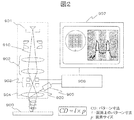
- FIG. 2 shows the principle of the length measurement SEM.
- the electron beam 910 emitted from the electron gun 901 is narrowed down by a focusing lens 902, and the surface of the sample 900 is adjusted by a deflector 903 controlled by a control unit 906 in a state where the objective lens 904 is focused on the surface of the sample 900. Dimensionally scanned.
- the secondary electrons 920 generated from the sample 900 by the irradiation of the electron beam 910 are captured by the detector 905 and processed by the control device 906, whereby an electron beam image as displayed on the CRT 907 is obtained. Since more secondary electrons are generated at the pattern edge portion, the electron beam image becomes a bright image at a portion corresponding to the pattern edge as displayed by the CRT 907.
- the dimension is obtained by multiplying the distance l (pixel) between edges on the electron beam image by the pixel size p (nm / pixel) (l ⁇ p).
- Patent Document 1 An example of length measurement processing in a length measurement SEM is described in Patent Document 1.
- a projection waveform is created by adding and averaging the signal waveform of the wiring in the longitudinal direction of the wiring from the local region in the image obtained by imaging the wiring to be measured, and the left and right wiring edges detected in this waveform Wiring dimensions are calculated as the distance between them.
- edge position detection methods for automatically calculating the inter-edge distance l.
- the widely used threshold method will be described.
- the threshold method is disclosed in Patent Document 2, for example.
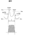
- the peak portions having a large signal amount corresponding to the left and right pattern edges are referred to as a left white band (left WB) and a right white band (right WB), respectively.
- the Max value and the Min value are obtained for each of the left and right WBs, a threshold level is calculated by internally dividing them by a predetermined ratio th (%), and the intersection position of the threshold and the signal waveform is It is defined as the edge position.
- a difference between measured values of a plurality of length measuring SEMs (hereinafter referred to as machine difference) becomes a problem.
- machine difference for example, as shown in Non-Patent Document 2, the machine difference in the DRAM half pitch 45 nm generation is ⁇ 0.18 nm, and the length difference in the 32 nm generation is ⁇ 0.13 nm, 22 nm generation. ⁇ 0.09nm is required as the machine difference.
- Non-Patent Document 2 discloses a method for measuring machine differences.
- the machine difference is defined as the difference between the measurement values of multiple SEMs.
- the length measurement SEM is contaminated by electron beam irradiation (amorphous carbon film adheres to the part irradiated with the electron beam of the sample).
- Phenomenon amorphous carbon film adheres to the part irradiated with the electron beam of the sample.
- shrink resist pattern shrinkage due to electron beam irradiation causes sample changes, so even if the same measurement object is measured by multiple devices and the difference between these measured values is simply calculated, It does not mean that the machine difference was measured correctly. This is because the difference in measured values includes the effect of sample changes.
- Non-Patent Document 2 shows a specific method for dealing with this problem. Here, two typical methods, ABBA method and grating method, are explained.
- Step1 At multiple locations on the sample (usually several tens), measure with device A and then with device B (AB sequence). From the average value of device B, the average value of device A Is obtained by subtracting ⁇ 1 (nm). The relationship of Formula 1 is established among ⁇ , ⁇ 1, and C1.
- a machine difference measurement method A method of correcting the machine difference by reducing the difference between different machines (hereinafter referred to as a machine difference measurement method) may be adopted.
- the machine difference between the devices A and B is measured by the ABBA sequence, and further between the devices A and C by the ACCA sequence. Since a procedure for measuring the machine difference is necessary, measuring the machine difference requires a great deal of labor.
- the grating method even if the measurement location is not biased, the effect of edge roughness remains, so there is a difference in pattern dimensions depending on the location, and in order to prevent this difference from being buried, (edge It is necessary to increase the number of measurement points considerably (depending on the degree of roughness).
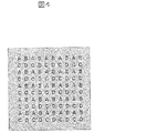
- the grating method is directly affected by the dimensional difference depending on the location. Much more measurement points are required. In FIG. 4, the number of measurement points for each apparatus is 25 points. However, in consideration of the above-described requirements for machine differences, it is often necessary to have 100 or more measurement points. As described above, both the ABBA method and the grating method require a great deal of labor to measure the machine difference, the ABBA method has an error factor of sample change, and the grating method has an error factor of pattern edge roughness. Because it exists, the correct machine difference is not always measured.
- machine differences vary depending on the cross-sectional shape (height, side wall inclination angle, etc.) and pattern density of the measurement object, so if you want to apply the machine difference measurement method strictly, There is a very troublesome problem that it is necessary to actually measure. This is because machine differences are caused by differences in incident beam characteristics and secondary electron detection characteristics between apparatuses.
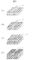
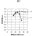
- simulation results of machine differences when various patterns 120, 121, 122, and 123 shown in FIGS. 5A to 5D are measured using two length measuring SEMs having different beam diameters are shown. 6 to 8 show.
- FIG. 6 shows (a) an isolated line pattern having a pattern height of 80 nm and a sidewall inclination angle of 0 ° (a pattern like the pattern 120 in FIG. 5A), and (b) a pattern height of 80 nm and a sidewall inclination angle of 10 °.
- FIG. 7A and 7C show the line and space pattern (pattern like the pattern 122 in FIG. 5C) in which the pattern height is 80 nm and the pattern pitch of the sidewall inclination angle is 0 ° is 45 nm.
- This is the result of calculating the machine difference when the line width is 15 nm to 45 nm. From this result, it can be seen that the machine difference is different when the pattern density is different.
- the line width is 25 nm or less
- the difference in machine difference between (a) and (c) is small because the pattern pitch in the line and space pattern is fixed at 45 nm in this simulation. This is because the distance to the line becomes far and the situation becomes similar to an isolated line pattern. It is clear that the change tendency of machine differences varies depending on the line width and pattern pitch. In order to apply the machine difference measurement method, it can be said that it is necessary to actually measure the machine difference for each pattern pitch and size.
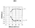
- FIGS. 8A and 8B show line widths of 15 nm to 45 nm for the above-mentioned (a) and (d) isolated space patterns having a pattern height of 80 nm and a sidewall inclination angle of 0 ° (patterns such as the pattern 123 in FIG. 5D). It is the result of calculating the machine difference.
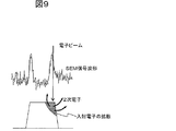
- the signs of the line pattern machine difference (a) and the space pattern machine difference (d) are reversed, as shown in FIG. This is because there is a relationship that the beam diameter is large and the peak portion is large.
- the situation is similar to (d). In this way, the machine difference varies depending on the topology of the measurement target. In order to apply the machine difference measurement method, it is necessary to measure the machine difference according to the topology.
- 6 to 8 show the result of simulating the case where the machine difference is caused by the difference in the beam diameter between the apparatuses, but other machine difference factors such as the difference in the tilt angle of the incident beam between the apparatuses.
- the machine difference differs depending on the cross-sectional shape (height, side wall inclination angle, etc.) and pattern density of the measurement object. The trend is different from the result.
- the machine difference measurement method requires a lot of work even for a single pattern.
- machine differences that are difficult to measure accurately must be implemented for each pattern to be measured. In situations where there are a wide variety of target patterns, this is not a realistic method.
- the present invention provides a machine difference correction method, a pattern dimension measuring method, a pattern dimension measuring system, and a method for monitoring changes over time of an electron microscope apparatus that can be applied to various cases.
- Step of modeling device characteristics In each length measuring SEM (# 1 to #n), a dedicated sample is imaged and the device characteristics parameters are obtained by analyzing the images. For example, the following (a) to (c) are performed.
- Beam diameter A knife edge pattern is imaged, and the beam diameter is calculated from the degree of blurring of the peak waveform at the edge portion.
- Beam tilt angle A pyramid shape pattern (quadrangular pyramid shape pattern) is imaged, and a beam tilt angle is calculated from the pyramid shape distortion on the image.
- (C) Brightness conversion coefficient Using a sample whose cross-sectional shape is known (measurement by an atomic force microscope or obtaining shape information by cross-sectional SEM observation), obtain an SEM signal waveform in the cross-sectional shape by SEM simulation, The brightness conversion coefficient between the simulation waveform and the actual waveform is calculated by comparing this with the actual signal waveform obtained by the length measurement SEM.
- Step of estimating machine difference An image of a measurement target pattern is captured by a reference device (for example, length measuring SEM # 1), and an MBL method (model-based library method, that is, an electron beam signal waveform of the measurement target pattern) Is applied to a library that associates the cross-sectional shape of the sample with the SEM signal waveform prepared in advance, and the cross-sectional shape of the measurement target pattern is estimated by a method of estimating the cross-sectional shape of the sample.
- a reference device for example, length measuring SEM # 1
- MBL method model-based library method, that is, an electron beam signal waveform of the measurement target pattern
- the machine difference measurement method which is a conventional method
- the machine difference measurement which requires a lot of time and labor and is difficult to measure accurately, must be carried out for all patterns to be measured.
- the machine difference is estimated in step (B).
- a pattern dimension measuring method (3) A plurality of electron microscope devices connected to each other via a network, a device parameter database storing device parameters of each of the plurality of electron microscope devices, and a first electron microscope that is one of the plurality of electron microscope devices Using the actual signal waveform of the image of the pattern of the dimension measurement target sample obtained by scanning the dimension measurement target sample using the apparatus, and the apparatus characteristic parameter of the first electron microscope apparatus stored in the apparatus parameter database Are compared with a simulation waveform library created by simulation to obtain an estimated cross-sectional shape of the pattern of the dimension measurement target sample, and the estimated cross-sectional shape of the pattern of the obtained dimension measurement target sample and the plurality of electron microscopes Device characteristic parameters of each of a plurality of electron microscope devices other than the first electron microscope among the devices , And a computer that generates a plurality of simulation signal waveforms corresponding to each of a plurality of electron microscope apparatuses other than the first electron microscope, and a calculation based on each of the plurality of simulation signal waveforms generated by the computer A
- a machine difference database storing machine differences between electron microscope apparatuses as machine difference information
- a recipe database storing recipes including processing for correcting dimensional measurement results using machine difference information stored in the machine difference database
- a pattern dimension measuring system (4)
- the machine difference correction method is characterized in that correction is performed with reference to a database storing differences in measurement results.
- (6) (a2) an electron microscope device, (b2) a system for measuring device characteristic parameters of the electron microscope device, and (c2) linking the device characteristic parameters of the electron microscope device with the date and time when the device characteristic parameters are calculated.
- a method for monitoring a time-dependent change of an electron microscope device characterized by presenting a time-dependent change in device characteristic parameters and a dimension measurement result.
- the present invention it is difficult to eliminate machine differences by adjusting the length measurement SEM hard wafer due to different types, etc., and it is difficult to deal with the machine difference measurement method, and there are a variety of measurement objects. It is possible to provide a machine difference correction method, a pattern dimension measurement method, a pattern dimension measurement system, and a method for monitoring a change with time of an electron microscope apparatus that can be applied to such cases.
- the device characteristic parameters of the length measuring SEMs 201-1 to 201-n are calculated using the device characteristic parameter calculation unit 301 in the device characteristic evaluation sample 101, and the result is stored in the device characteristic parameter database 401.
- the desired apparatus characteristics are the difference between the tilt angle of the irradiation beam, the beam diameter of the irradiation beam, and the detection efficiency of secondary electrons emitted from the sample.
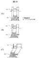
- the difference in the beam diameter of the irradiation beam causes a machine difference, and the fact that the machine difference changes depending on the cross-sectional shape, pattern density, and dimensions is described with reference to FIGS. That's right.
- Reference numeral 150 in FIG. 18A schematically represents a signal waveform when a beam having a trapezoidal cross-sectional shape with a side wall inclination angle ⁇ is irradiated with a beam from vertically above (FIG. 10). As shown, the secondary electron intensity is higher at the edge portion).
- the threshold shown in FIG. 3 is applied to this signal waveform, the dimension measurement value becomes CDa.
- 151 in FIG. 18B is a signal waveform when the beam tilt angle is ⁇ 1. If the threshold method is similarly applied to this signal waveform, the dimension measurement value is CDb.
- reference numeral 152 denotes a case where ⁇ 2 has a larger beam tilt angle.
- the dimension measurement value at this time is CDc.
- CDa CDb, CDa ⁇ CDc.
- the difference in beam tilt angle between devices can be a factor of machine difference.
- the difference depends on the cross-sectional shape, pattern density, and dimensions of the measurement target.
- FIG. 18 is a schematic diagram, and the dependency on the pattern density and size does not appear. However, since the signal waveform actually changes depending on the pattern density and size, the impact of the change in the tilt angle changes accordingly. it is obvious).
- the measurement of the tilt angle of the irradiation beam will be described with reference to FIG.
- the method described in JP-A-2005-183369 is suitable for measuring the tilt angle of the irradiation beam.
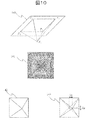
- a sample in which concave or convex pyramid shapes (quadratic pyramids) prepared by the crystal anisotropic etching technique are arranged is used.
- An example of a concave pyramid shape is shown at 140 in FIG.
- Crystal anisotropic etching technology is the production of triangular peaks and step structures based on crystal planes by utilizing the fact that the etching rate differs for each crystal plane when a specific etching solution is applied to a single crystal. Technology.
- the angles formed by the side surfaces (four side surfaces in FIG.
- a pyramid-shaped SEM image is shown at 141. Since the secondary electron intensity at the inclined part is larger than the secondary electron intensity at the flat part, the side wall of the pyramid is brighter than the flat part on the SEM image.
- Reference numeral 141 denotes a case where the beam irradiation angle is not tilted. When the beam irradiation angle is tilted, for example, the situation is 142. As in 143, the edge line and the edge line on the bottom surface of the pyramid are detected by image processing, and the deviation ⁇ x in the x direction and the deviation ⁇ y in the y direction of the intersection of the pyramid ridge lines are obtained.
- ⁇ x reflects the beam tilt angle change ⁇ x in the x direction
- ⁇ y reflects the beam tilt angle change ⁇ y in the y direction.
- the beam tilt angles ⁇ x and ⁇ y can be calculated from ⁇ x and ⁇ y.
- the above-described pyramid sample is used as a device characteristic evaluation sample, and an image of the pyramid sample is acquired by each of the length measurement SEMs 201-1 to 201-n.
- the beam tilt angle of the length measuring SEM is calculated, and the result is stored in the apparatus characteristic parameter database 401.
- the advantage of using the pyramid sample is that the angle formed by the four sides is known, so that the beam tilt angle can be calculated by applying a given formula.
- Another advantage is that this method can be used for other machine differences. It is difficult to be influenced by factors.
- the difference in the beam diameter of the irradiation beam between the length measurement SEMs appears as a difference in the sharpness of the edge on the image, but the above method calculates the tilt angle based on the geometric deformation of the pyramid shape. It is hardly affected by the difference in sharpness of the edge portion.
- the difference in secondary electron detection efficiency between the length measurement SEMs appears as a difference in brightness and S / N on the image, but this difference does not affect the measurement result of the tilt angle.
- Equation 170 the dynamic range is adjusted by convolving Gauss (x) corresponding to the beam intensity distribution with respect to the signal waveform Isim (x) when the beam diameter is zero. Modeling is performed when the result of multiplying the coefficient scale and adding the coefficient offset for adjusting the offset becomes the actual signal waveform Ireal (x) waveform. Therefore, Gauss (x), scale, and offset should be determined as device characteristic parameters.
- Gauss (x) the ⁇ value of the Gaussian function is a parameter to be determined.
- a desirable device characteristic evaluation sample for calculating these parameters includes a step edge sample with a known cross-sectional shape, for example, an NCD line width standard manufactured by VLSI Standard, USA.
- 161 indicates a step edge
- 162 indicates a signal waveform of the step edge
- 190 and 191 show examples of SEM photographs of the step edge.
- a silicon oxide film / silicon / silicon oxide film stack was mounted vertically on the wafer and the silicon oxide film was etched, leaving the silicon part in a line pattern. In terms of its creation principle, it has a vertical edge (side wall tilt angle 0 °), which is desirable for calculating the above parameters.
- Isim (x) is calculated from the signal signal waveform at the step edge when the beam diameter is zero by SEM simulation (step S310).
- the measurement result of the tilt angle of the irradiation beam measured by the method shown in FIG. 11 is reflected. That is, in the SEM simulation, the electron implantation angle with respect to the sample is matched with the measurement result of the tilt angle.
- a side-length SEM image 151 of the step edge is picked up and an actual signal waveform Ireal (x) is obtained (step S311).
- Gauss (x), Scale, and Offset that satisfy Expression 170 are obtained using the obtained Isim (x) and Ireal (x) (step S312).
- Gauss (x), Scale, and Offset are sequentially changed, and the degree of divergence between the right side and the left side (for example, the sum of squares of the differences) is obtained each time.
- a method is used in which the calculation is repeated until the value becomes less than or equal to. For example, a non-linear optimization method such as the LM method (Levenberg-Markert method) can be applied.
- An example of the result of step S312 is shown in a balloon.
- a waveform 180 is the left side of Expression 170
- a waveform 181 is the right side when the determined Gauss (x), Scale, and Offset are substituted.
- the above-mentioned NCD line width standard sample is used as a device characteristic evaluation sample, the image is acquired by each of the length measurement SEMs 201-1 to 201-n, and each length measurement is performed by the device characteristic parameter calculation unit 301. Gauss (x), Scale, and Offset are calculated for each SEM, and the result is stored in the device characteristic parameter database 401.
- the advantage of using the NCD line width standard sample is that it is guaranteed that the sample has a vertical edge (side wall tilt angle 0 °), so that the actual measurement of the cross-sectional shape is unnecessary, and the edge near vertical There are two points that the shape is more sensitive to changes in the beam diameter (in this case, changes in the ⁇ value of the Gaussian function) than the edge shape having a taper.
- the parameter calculation step in this case is shown in FIG. In FIG. 12, the cross-sectional shape of the sample is measured in the first step S320.
- the balloon in S320 schematically shows the result of measuring the line pattern extending in the y direction with an atomic force microscope. Measurement results for the number of scans with an atomic force microscope can be obtained, and these are averaged to obtain the average cross-sectional shape.
- step S321 the SEM simulation is performed using the cross-sectional shape obtained in the previous S320 as an input, and a simulation waveform Isim (x) when the beam diameter in the obtained cross-sectional shape is zero is calculated. Thereafter, similarly to steps S311 and S312 shown in FIG. 11, steps S322 and S323 are performed to obtain Gauss (x), Scale, and Offset.
- the steps for machine difference prediction will be described with reference to FIG.
- the sample 102 that is the dimension measurement target is imaged by the SEM # 1
- the cross-sectional shape of the measurement target pattern is estimated by the MBL system 302 (details will be described later)
- the SEM simulator 303 estimates the cross-sectional shape.
- a signal waveform of each length measuring SEM is generated.
- the length measuring unit 304 measures the signal waveform dimensions of each SEM, the difference between them is obtained by the machine difference calculating unit 305, and the result is stored in the machine difference database 402.
- FIG. 13 and 14 explain the processing contents in the MBL system.
- MBL method model-based library matching method
- SEM waveforms in various cross-sectional shapes are calculated in advance by SEM simulation, and this is matched with an actual waveform.
- This is a method for estimating the cross-sectional shape of an object.
- FIG. 13 shows documents “J. S. Villarrubia, A. E. Vladar, J. R. Lowney, and M. T. Postek,“ Scanning electron microscope analog of scatterometry, ”Proc. Of the SPIE, Vol. 4689, pp. 304-312 (2002) ”.
- the apparatus characteristic parameter 401 and the neighboring pattern information 316 are input.
- the tilt angle of the irradiation beam and Gauss (x), scale, and offset are stored in the apparatus characteristic parameter database.
- the device parameters of SEM # 1 are extracted from the database, and these values are substituted when generating a signal waveform by SEM simulation. Note that the same SEM simulator 311 as that used in S310 of FIG. 11 or S321 of FIG. 12 may be used.
- the neighboring pattern information for example, pattern pitch
- the library 312 takes into consideration the actual device state and the influence of neighboring patterns.
- the sectional shape 315 of the dimension measurement target is estimated.
- FIG. 14 only the side wall inclination angle ⁇ is used as a parameter as a shape variation to simplify the explanation. However, in order to make it more accurate, this parameter is suitable for expressing the shape according to the measurement target.
- top and bottom are rounded, or if the side wall inclination angle is different between the upper side and the lower side, the upper side wall inclination angle and the lower side wall inclination angle, etc.
- the upper side wall inclination angle and the lower side wall inclination angle, etc. may be input as appropriate.
- neighboring pattern information design data or the like of a dimension measurement target sample may be used as appropriate.
- the length measuring SEM # 1 (201-1) has already been imaged with the SEM image 314 of the dimension measurement target pattern (to be used in step 302 in FIG. 1, ie, in the step of estimating the cross-sectional shape by the MBL system).
- the dimension 331 is calculated by applying a predetermined edge detection method such as a threshold method (see FIG. 3) to the actual signal waveform 330 of the SEM image 314.
- the device parameter 410 of # 2 is taken out from the device parameter database (not shown), and the cross-sectional shape 315 of the pattern to be measured previously estimated is input to the SEM simulator 303 as a simulation.
- a signal waveform 332 is generated, and a threshold value method or the like is calculated for the signal waveform 332 to calculate the dimension 333.
- a difference between the dimension 331 and the dimension 333 is obtained (334), and the result is stored in the machine difference database 402.
- the machine difference database 402 stores the predicted machine difference of the dimension measurement target pattern.
- FIG. 15 shows an example in which the machine difference between the side master SEM # 1 and another side master SEM is shown.
- the present invention is not limited to this, and all machine differences between the devices may be obtained and stored.
- FIG. 17 is an example of a GUI for creating a recipe displayed on the screen of the computer 300.
- Check items 615 to 617 are items that are turned ON when measurement of a pattern dimension at a desired height is required.
- the cross-sectional shape of the measurement target pattern has been estimated by the MBL system (302 in FIG. 1)
- the difference between the dimension measurement result of SEM # 1 and the bottom dimension obtained from the cross-sectional shape estimated by the MBL system is ⁇ bottom
- the dimension measurement result of SEM #i is CDi
- the machine difference database If the machine difference from the described SEM # 1 machine is di, when the bottom dimension 615 is turned on in SEM # i machine, the bottom dimension is calculated by Equation 4 and output as one item of the measurement result.
- the (Formula 4) Bottom dimension CDi-di- ⁇ bottom
- 610 is an item when the cross-sectional shape of the dimension measurement target pattern is handled as a trapezoid. For example, as described above, two trapezoids having different upper side wall inclination angles and lower side wall inclination angles are stacked. In the case of a simple shape, it goes without saying that the items of 610 are adapted accordingly.
- the length measurement step will be described with reference to FIG.
- the dimension measurement in each device is performed according to the description of the recipe as described above.
- the measurement length correction SEM # n machine is selected with machine difference correction (when 611 in FIG. 17 is ON)
- the dimension measurement target sample is measured by the dimension measurement SEM # n machine 201-n.
- the machine difference of SEM # n is read from the machine difference database, and the dimension measurement result is corrected, whereby the final dimension measurement target sample dimension is measured.
- the dimension measurement result has a machine difference, but after passing through the machine difference correction unit 306-n, the measurement value has no machine difference.
- the items etc. specified by the GUI of FIG. 17 are output.
- FIG. 17 a system configuration example of a pattern dimension measuring system corresponding to machine differences according to the present invention will be described.
- This system is imaged with a plurality of length measurement SEMs 201-1, 201-2,... 201-n connected to the local area network 500, a recipe database 501 for storing length measurement SEM recipes, and a length measurement SEM.
- a database 400 for storing the SEM image, a database 401 for storing apparatus parameters, a database 307 for storing machine differences, and a computer 300 are used as appropriate.
- the computer 300 performs various processes such as device parameter calculation (301), cross-sectional shape estimation (302) by the MBL system, and SEM signal waveform generation (303) by SEM simulation shown in FIG. All of these use a common SEM simulator, and if an SEM image acquired in advance by a length measurement SEM is stored in the image database 400, all can be executed offline. Thus, it is desirable to provide a computer as a dedicated computer. A computer that performs input / output and a computer that performs the above-described processes may be provided separately.
- a line-shaped pattern is shown as a measurement target in FIG. 5, the target of the present invention is not limited to a line pattern.
- the same machine difference correction method and pattern dimension measurement method corresponding to the machine difference can be applied to the measurement of the hole pattern as shown in FIG. 19 and measurement of other arbitrary shapes.
- signal waveforms are obtained for each direction (in FIG. 19, 0 degrees, 45 degrees, 90 degrees, and 135 degrees), and edge detection is performed on each signal waveform by a threshold method or the like.
- the average value of the dimension measurement results in all directions is output as the hole diameter.
- the input shape is a hole
- the hole interval is input as neighborhood pattern information
- the library is created
- waveform matching is performed.
- Step 313 is performed to obtain the cross-sectional shape of the hole in a predetermined direction. This is performed for each direction (in the case of the measurement method of FIG. 19, four directions of 0 degrees, 45 degrees, 90 degrees, and 135 degrees).
- the SEM simulation is performed with the cross-sectional shape in each direction as an input, the signal waveform is obtained, the dimensions are measured, and the average value in all directions may be set as the hole diameter.
- the dimension can be measured.
- the machine difference correction method for a plurality of length measuring SEMs and the pattern dimension measurement method corresponding to the machine difference have been described.
- the present invention can be used for monitoring changes with time of various apparatuses. Is also applicable.
- the details of the processing performed in the second embodiment are the same as the processing described in the first embodiment, and therefore, differences will be mainly described.
- the device characteristic parameters are calculated periodically (step 301 in FIG. 1), and the device parameters are input to the SEM simulator to generate the SEM signal waveform. Then, dimension measurement is performed (steps 303 and 304 in FIG. 1 are performed).
- the device characteristic parameter calculated periodically is linked to the calculated date and stored in the database.
- the device characteristic parameter calculated periodically is linked to the calculated date and stored in the database.
- FIG. 20 by displaying the date and time on the horizontal axis and the device parameters and dimension measurement results on the vertical axis, it is possible to confirm the degree of change over time of the apparatus and to obtain a hint of the cause of change over time of the apparatus.
- the beam tilt angle fluctuates, the optical axis shifts, the electron gun deterioration occurs when the beam diameter changes, and the irradiation beam current changes when the scale value changes.
- the calculation of the device characteristic parameter is not necessarily performed periodically, and may be performed irregularly.
- the above method can be used to determine the impact on dimensional measurement results. In other words, if there is a change in the dimension measurement result, an immediate measure is necessary, and if there is no change in the dimension measurement result, it can be determined that an immediate measure is unnecessary.
- the present embodiment is advantageous in terms of accuracy as compared with the conventional temporal change monitoring method.
- a method such as the grating method described in the background art has been used to change the apparatus over time (the ABBA method cannot be applied because the time cannot be traced back).
- the ABBA method cannot be applied because the time cannot be traced back.
- many time points on the sample were measured, the average value was obtained, and the results were compared with past results to monitor changes over time of the device.
- the grating method has a problem in that accuracy without using a considerable number of measurement points cannot be obtained.
- the size changes due to the formation of an oxide film on the surface, and the extent of the change depends on the material and the storage state of the sample.
- the possibility of a change with time of the device characteristic evaluation sample 101 used in the device characteristic modeling step of FIG. 1 cannot be completely denied, but the pyramid sample shown in FIG. Even if the step edge samples shown in FIG. 11 are used, it is considered that the surface oxide film hardly affects the device characteristic parameters extracted using these samples. In the case of the pyramid sample, since only the angle formed by the four side surfaces is used as known information, if this does not change, the measurement result of the beam tilt angle is not affected. The same applies to the step edge sample.
- the output dimension measurement result is a predicted value of the dimension measurement result when the apparatus state changes, so that it can be determined whether it is due to the apparatus change over time or the sample over time. The lack of it does not matter.
- the present invention is not limited to the above embodiment, and various modifications can be made without departing from the scope of the invention. Not too long.
- the beam tilt angle, the beam diameter (Gauss (x)), and the brightness conversion coefficient (scale, offset) are measured as the apparatus characteristic parameters.
- the present invention is not limited to these, and when there is an apparatus characteristic parameter that affects other dimension measurement results, it may be appropriately used as a measurement target.
- the biggest problem in the conventional aging monitor which is the problem of being unable to discriminate between the aging of the sample and the aging of the apparatus, is solved, and is more accurate. A change with time can be monitored.
Landscapes
- Physics & Mathematics (AREA)
- Chemical & Material Sciences (AREA)
- Analytical Chemistry (AREA)
- General Physics & Mathematics (AREA)
- Electromagnetism (AREA)
- Health & Medical Sciences (AREA)
- General Health & Medical Sciences (AREA)
- Nuclear Medicine, Radiotherapy & Molecular Imaging (AREA)
- Radiology & Medical Imaging (AREA)
- Length-Measuring Devices Using Wave Or Particle Radiation (AREA)
Abstract
予め,各測長SEMの装置特性パラメタを計測しておき,MBL(モデル・ベース・ライブラリマッチング)システムにて寸法計対象の断面形状を推定し,前記推定した断面形状と前記装置特性パラメタを入力としてSEMシミュレーションにより信号波形を生成して寸法計測を行って,寸法計測結果の差を機差として登録しておく。本番の計測では,各測長SEMでの寸法計測結果から,前記登録された機差を減ずることで機差を補正する。また,上記の装置特性パラメタの計測と,上記寸法計測結果の予測を定期的に行うことで、測長SEMの経時変化をモニタする。本発明によれば,大変な手間と時間を要する機差の実測が不要となる。また,装置の経時変化モニタにおいて問題となる,試料の経時変化の影響を排除することが可能となる。
Description
本発明は半導体装置等の微少寸法を計測するのに用いられる電子顕微鏡装置のパターン寸法計測に関する。
非特許文献1に述べられているように,半導体プロセスにおいてパターン寸法管理ツールとしても最も普及しているのは,走査電子顕微鏡(以下SEMと略す)を半導体計測専用に特化した測長SEMである。図2に測長SEMの原理を示す。電子銃901から放出された電子ビーム910は集束レンズ902で細く絞られ,対物レンズ904で焦点を試料900の表面に合わせた状態で制御装置906で制御された偏向器903により試料900上を2次元的に走査される。電子ビーム910の照射によって試料900から発生した二次電子920を検出器905で捕らえて制御装置906で信号処理することで、CRT907に表示されているような電子線像が得られる。二次電子はパターンエッジ部でより多く発生するため,電子線像は,CRT907で表示されているように、パターンエッジに相当する部分が明るい画像となる。測長SEMにおいては,電子線像上でのエッジ間距離l(画素)に画素サイズp(nm/画素)を乗じる(l×p)ことにより寸法が求められる。
測長SEMにおける測長処理の一例が特許文献1に記載されている。特許文献1の開示例においては,測定対象配線を撮像した画像内の局所領域から,配線の信号波形を配線の長手方向に加算平均した投影波形を作成し,この波形において検出した左右の配線エッジ間の距離として配線寸法を算出している。
エッジ間距離lを自動計算するためのエッジ位置検出方法として種々の方法が提案されているが,ここでは,広く一般的に用いられている,しきい値法について述べる。
しきい値法は,例えば、特許文献2に開示されている。図3で示すように,左右のパターンエッジに相当する信号量の大きいピーク部分を,それぞれ左ホワイトバンド(左WB),右ホワイトバンド(右WB)と呼ぶことにする。しきい値法は,左右WBそれぞれで,Max値,Min値を求め,これらを所定の比率th(%)で内分するしきい値レベルを算出し,しきい値と信号波形の交差位置をエッジ位置と定義する。
半導体デバイスパターンの微細化により,計測精度に対する要求は年々厳しさを増している。測長SEMの場合,一つの半導体製造ラインに複数台の測長SEMが投入され,これらを併用することが多いため,単一の測長SEMの計測再現性のみならず,装置間の計測再現性,すなわち,複数台の測長SEMの計測値間の差(以下,機差と記す)が問題となる。機差に対する要求については、例えば、非特許文献2で示すように、DRAMハーフピッチ45nm世代での機差として<0.18nm,同32nm世代での測長値機差として<0.13nm,同22nm世代での機差として<0.09nmが要求されている。
また,非特許文献2には機差の測定方法が開示されている。前述のように,機差は複数台のSEMの計測値の差と定義されるが,測長SEMは,電子線照射によってコンタミネーション(試料の電子線を照射した部分にアモルファスカーボン膜が付着する現象),試料帯電,あるいは,シュリンク(電子線照射によるレジストパターンの縮み)といった試料変化を引き起こすため,同一計測対象を複数の装置で計測し、単純にそれらの計測値の差を求めても,機差を正しく測定したことにはならない。計測値の差には,試料変化の影響が含まれてしまうからである。非特許文献2にはこの問題に対処するための具体的な方法が示されている。ここでは,二つの代表的な手法,ABBA法とグレーティング法を説明する。
(1)ABBA法
装置Aに対する装置Bの機差をδ(nm),装置Aでの計測が引き起こすコンタミネーション,試料帯電,シュリンク起因の計測値変化量をc1(nm)と,装置Bでの計測が引き起こすによる計測値変化量をc2(nm)とする。次に示す,step1~step3にて機差を求める。
Step1:試料上の複数箇所(通常は数十箇所)について,装置Aで計測した後に装置Bで計測を行い(ABシーケンス),装置Bの計測値の平均値から装置Aの計測値の平均値を減じた値δ1(nm)を求める。δ,δ1,C1の間には数式1の関係が成り立つ。
(数1)δ1=δ+C1
Step2:試料上の複数箇所(通常は数十箇所)について,装置Bで計測した後に装置Aで計測を行い(BAシーケンス),装置Aの計測値の平均値から装置Bの計測値の平均値を減じた値δ2(nm)を求める。δ,δ2,C2の間には数式2の関係が成り立つ。
(数2)δ2=-δ+C2
Step3:仮にC1=C2が成り立つならば(装置Aと装置Bが引き起こす試料変化が同程度であるならば),数式1と数式2より,
(数3)δ=(δ1-δ2)/2
にて,δが求められる。
ABBA法はc1=c2の仮定が成り立ち(装置Aと装置Bが引き起こす試料変化が同程度とみなせるということ),かつ,個々の計測の計測誤差を考慮して,計測点数を十分に多くすれば正しい機差を求めることができる。
装置Aに対する装置Bの機差をδ(nm),装置Aでの計測が引き起こすコンタミネーション,試料帯電,シュリンク起因の計測値変化量をc1(nm)と,装置Bでの計測が引き起こすによる計測値変化量をc2(nm)とする。次に示す,step1~step3にて機差を求める。
Step1:試料上の複数箇所(通常は数十箇所)について,装置Aで計測した後に装置Bで計測を行い(ABシーケンス),装置Bの計測値の平均値から装置Aの計測値の平均値を減じた値δ1(nm)を求める。δ,δ1,C1の間には数式1の関係が成り立つ。
(数1)δ1=δ+C1
Step2:試料上の複数箇所(通常は数十箇所)について,装置Bで計測した後に装置Aで計測を行い(BAシーケンス),装置Aの計測値の平均値から装置Bの計測値の平均値を減じた値δ2(nm)を求める。δ,δ2,C2の間には数式2の関係が成り立つ。
(数2)δ2=-δ+C2
Step3:仮にC1=C2が成り立つならば(装置Aと装置Bが引き起こす試料変化が同程度であるならば),数式1と数式2より,
(数3)δ=(δ1-δ2)/2
にて,δが求められる。
ABBA法はc1=c2の仮定が成り立ち(装置Aと装置Bが引き起こす試料変化が同程度とみなせるということ),かつ,個々の計測の計測誤差を考慮して,計測点数を十分に多くすれば正しい機差を求めることができる。
(2)グレーティング法
グレーティング法では,電子線照射による試料変化の影響を避けるため,同じ箇所を複数回計測せずに、図4のように、4台の装置(A,B,C,D)の機差を測定する際の計測箇所の配置をずらし、各装置は多数のフレッシュな箇所(一度も撮像されたことない箇所)を計測して,それらの平均値の差を機差とする。
この際、パターンの出来映えの面内分布の影響を受けづらいよう,各装置の計測箇所は偏らないように配置される。
グレーティング法では,電子線照射による試料変化の影響を避けるため,同じ箇所を複数回計測せずに、図4のように、4台の装置(A,B,C,D)の機差を測定する際の計測箇所の配置をずらし、各装置は多数のフレッシュな箇所(一度も撮像されたことない箇所)を計測して,それらの平均値の差を機差とする。
この際、パターンの出来映えの面内分布の影響を受けづらいよう,各装置の計測箇所は偏らないように配置される。
社団法人 日本半導体製造装置協会(SEAJ)平成17年度半導体製造装置技術ロードマップ報告書 第5編計測
International SEMATECH Manufacturing Initiative, "Unified Advanced Critical Dimension Scanning Electron Microscope (CD-SEM) Specification for sub-90 nm Technology (2008 Version)," ISMI Technology Transfer #04114595E-ENG
先に述べた機差に対する要求に応えるべく,測長SEMベンダ各社では機差低減のための努力が継続されているが,測長SEMの運用状況によっては,種々の型式の装置が混在していることもあるため,型式間に性能の違い(例えば分解能の違いなど)がある以上,機差の発生は避けがたい。こうした場合の対策として、本番の計測に先立ち機差を実測して(ABBA法やグレーティング法による)装置別機差として登録しておき,本番の計測時には各装置による寸法計測値から,上記の装置別機差を減ずることで機差を補正するという方法(以下,これを機差実測方式と呼ぶ)が採用されることもある。
しかしながら,ABBA法では、例えば、対象装置が3台(A,B,C)の場合は,ABBAシーケンスによって装置A,B間の機差を測定し、さらに,ACCAシーケンスによって装置A,C間の機差を測定するといった手順が必要であるため、機差測定には多大な手間を要する。また、グレーティング法では、計測箇所が偏らないようにしても,エッジラフネスの影響は残っているので,場所によってパターン寸法に差があり、この差に機差が埋もれないようにすべく、(エッジラフネスの程度によるが)計測点数を相当大きくすることが必要である。グレーティング法は,ABBA法での前提条件c1=c2が成り立たない場合にも適用可能という利点はあるが,ABBA法と異なり,場所による寸法差の影響をダイレクトに受けるため,原理上,ABBA法よりずっと多くの計測点数を必要とする。図4では装置ごとの計測点数は25点であるが,前述の機差に対する要求を考慮すると,100点以上の計測点数が必要になることも少なくない。
このように、ABBA法にしてもグレーティング法にしても機差測定には多大な手間を要す上,ABBA法には試料変化という誤差要因が,グレーティング法にはパターンのエッジラフネスという誤差要因が存在するため,必ずしも正しい機差が測定されるとは限らない。
このように、ABBA法にしてもグレーティング法にしても機差測定には多大な手間を要す上,ABBA法には試料変化という誤差要因が,グレーティング法にはパターンのエッジラフネスという誤差要因が存在するため,必ずしも正しい機差が測定されるとは限らない。
さらに,機差は,計測対象の断面形状(高さや側壁傾斜角など)やパターン密度によって異なるため,機差実測方式を厳密に適用しようとするならば,全ての計測対象パターンについて,機差を実測することが必要となるという非常にやっかいな問題がある。これは,機差が,装置間の入射ビーム特性や2次電子検出特性の違いによって生じるということに起因する。例として,図5(A)~(D)に示す各種のパターン120、121,122、123を,ビーム径が異なる2台の測長SEMを用いて計測した場合の機差のシミュレーション結果を図6~図8に示す。
シミュレーションでは,ビーム径が5nm(σ=2.5nmのガウシアンビーム)の場合のSEM信号波形と,ビーム径が6nm(σ=3nmのガウシアンビーム)の場合のSEM信号波形をモンテカルロシミュレーションにて求め,それぞれの波形に対してしきい値法(図3参照)を適用し寸法を算出し,ビーム径が6nmの場合の寸法計測値とビーム径が5nmの場合の寸法計測値の差を機差として求めた。
図6は,(a)パターン高さ80nm,側壁傾斜角0°の孤立ラインパターン(図5(A)のパターン120のようなパターン)と,(b)パターン高さ80nm,側壁傾斜角10°の孤立ラインパターン(図5(B)のパターン121のようなパターン)について,線幅が15nm~45nmにおける機差を算出した結果である。この結果から,側壁傾斜角が異なると機差が異なるということが分かる。機差実測方式を適用するためには,側壁傾斜角別に機差を実測することが必要といえる。
図7は,上記(a)と,(c)パターン高さ80nm,側壁傾斜角0°のパターンピッチが45nmのライン・アンド・スペースパターン(図5(C)のパターン122のようなパターン)について,線幅が15nm~45nmにおける機差を算出した結果である。この結果から,パターン密度が異なると機差が異なるということが分かる。なお,線幅が25nm以下では,(a)と(c)の機差の違い小さいのは,本シミュレーションではライン・アンド・スペースパターンでのパターンピッチを45nmに固定したため,線幅が小さくなると隣接ラインまでの距離が遠くなって,孤立ラインパターンに近い状況になるためである。線幅やパターンピッチに依存して,機差の変化傾向が異なることは明らかであり,機差実測方式を適用するためには,パターンピッチ,サイズ別に機差を実測することが必要といえる。
図8は,上記(a)と,(d)パターン高さ80nm,側壁傾斜角0°の孤立スペースパターン(図5(D)のパターン123のようなパターン)について,線幅が15nm~45nmにおける機差を算出した結果である。ラインパターンの機差(a)と,スペースパターンの機差(d)の符号が逆転するのは、図9に示すように、エッジ部においては2次電子信号波形のピーク部が一定の広がりを有し,ビーム径大→ピーク部の広がり大という関係があるからである。スペース計測の他,ホールパターンの径を計測するような場合も,(d)と同様の状況となる。このように,計測対象のトポロジーによっても機差は異なる。機差実測方式を適用するためには,トポロジーに応じて機差を実測することが必要といえる。
図6~図8は,装置間のビーム径の違いによって機差が生じている場合をシミュレートした結果であるが,他の機差要因,例えば,入射ビームのチルト角の装置間差,あるいは,2次電子の検出効率の装置間差が存在する場場合,やはり,計測対象の断面形状(高さや側壁傾斜角など)やパターン密度によって機差が異なるが,その異なり方は,上記のシミュレーション結果とは異なった傾向となる。
以上のように、機差実測方式は,単一のパターンですら大変な手間を要し,加えて,正確な測定が難しい機差を計測対象パターンごとに実施しなければならず,特に,計測対象パターンが多岐に及ぶような状況では,現実的な方法とは言い難い。
本発明は,型式が異なる等の理由で,測長SEMのハードウエハの調整では機差をなくすことが困難であり,また,機差実測方式では対応が困難な,計測対象が多岐に及ぶようなケースにも適用が可能な機差補正方法、パターン寸法計測方法、パターン寸法計測システムおよび電子顕微鏡装置の経時変化のモニタ方法を提供するものである。
本願において開示される発明のうち代表的なものの概要を簡単に説明すれば次のとおりである。
(1)本発明は,次の(A)~(C)のステップにて,機差を補正,すなわち,機差のない計測値を得るものである。
(A)装置特性性をモデル化するステップ:各測長SEM(#1号機~#n号機)において,専用試料を撮像し,画像を解析することで装置特性パラメタを求める。例えば,次の(a)~(c)を行う。
(a)ビーム径:ナイフエッジパターンを撮像し、エッジ部におけるピーク波形のぼけの程度からのビーム径を算出する。(b)ビームチルト角:ピラミッド形状パターン(四角錐形状パターン)を撮像し,画像上のピラミッド形状の歪みからビームチルト角を算出する。(c)明るさ変換係数:断面形状が既知(原子間力顕微鏡による計測,あるいは,断面SEM観察によって形状情報を得る)のサンプルを用い,その断面形状におけるSEM信号波形をSEMシミュレーションにて求め,これと,測長SEMによる実信号波形とを比較することで,シミュレーション波形と実波形の間の明るさ変換係数を算出する。
(B)機差を推定するステップ:基準装置(例えば,測長SEM#1号機)で計測対象パターンを撮像し,MBL法(モデル・ベース・ライブラリ法,すなわち,計測対象パターンの電子線信号波形を予め作成しておいた試料の断面形状とSEM信号波形とを関連づけるライブラリに当てはめることによって,試料の断面形状を推定する方法)にて計測対象パターンの断面形状を推定する。この断面形状を入力として,装置パラメタ(上記(A)で算出)を反映させたSEMシミュレーションを行って,#2号機~#n号機のSEM信号波形を求め,所定のエッジ検出手法(前記のしきい値法など)を適用して寸法計測を行い,これと,測長SEM#1号機の寸法計測結果を比較することで,各測長SEMの基準装置に対する機差を推定する。
(C)測長のステップ:各測長SEM(#1号機~#n号機)で通常通りに,計測対象パターンの計測を行い,非基準装置(#2号機~#n号機)については,得られた計測結果から,上記(B)で推定した機差を減ずる。
従来の手法である機差実測方式の場合,大変な手間と時間を要し,かつ,正確な測定が難しい機差測定を,全計測対象パターンについて実施しなければならないのに対し,本発明では,上記(A)のステップで予め装置特性パラメタを計測しておけば,上記(B)のステップで機差が推定される。
また、本発明によれば,上記(B)で推定した機差を補正値として用いることによって,計測対象が多岐に及ぶようなケースにも適用が可能な機差補正方法を提供することが可能となる。これにより,型式が異なる測長SEMが混在している場合であっても,これらの混用が可能となる。
(2)互いにネットワークで接続された複数の電子顕微鏡装置の一つである第一の電子顕微鏡装置を用いて寸法測定対象試料を走査し、前記寸法測定対象試料のパターンの画像を取得するステップと、前記取得した前記寸法測定対象試料のパターンの画像の実信号波形と、予め格納された前記複数の電子顕微鏡装置の装置特性パラメタのうち前記第一の電子顕微鏡装置の装置特性パラメタを用いてシミュレーションにより作成したシミュレーション波形ライブラリと、を比較して、前記寸法測定対象試料のパターンの推定断面形状を得るステップと、前記得られた寸法測定対象試料のパターンの推定断面形状と、前記複数の電子顕微鏡装置のうち前記第一の電子顕微鏡以外の複数の電子顕微鏡装置各々の装置特性パラメタと、を用いて、前記第一の電子顕微鏡以外の複数の電子顕微鏡装置各々に対応する複数の模擬信号波形を生成するステップと、前記実信号波形に基づいて算出した前記寸法測定対象試料のパターンの寸法と前記複数の模擬信号波形各々に基づいて算出した複数の前記寸法測定対象試料のパターンの寸法とを用いて、前記第一の電子顕微鏡を含めた複数の電子顕微鏡装置各間の機差を算出し、算出された前記複数の電子顕微鏡装置各間の機差を機差情報として機差データベースに格納するステップと、前記複数の電子顕微鏡装置の少なくとも一つを用いて得られた前記寸法計測対象試料のパターンの寸法計測結果を、前記機差データベースに格納された機差情報を用いて補正して、前記寸法計測対象試料のパターンの寸法を計測するステップと、を有することを特徴とするパターン寸法計測方法である。
(3)互いにネットワークで接続された複数の電子顕微鏡装置と、前記複数の電子顕微鏡装置各々の装置パラメタを格納する装置パラメタデータベースと、前記複数の電子顕微鏡装置の一つである第一の電子顕微鏡装置を用いて寸法測定対象試料を走査することにより取得した寸法測定対象試料のパターンの画像の実信号波形と、前記装置パラメタデータベースに格納された前記第一の電子顕微鏡装置の装置特性パラメタを用いてシミュレーションにより作成したシミュレーション波形ライブラリと、を比較して、前記寸法測定対象試料のパターンの推定断面形状を得、前記得られた寸法測定対象試料のパターンの推定断面形状と、前記複数の電子顕微鏡装置のうち前記第一の電子顕微鏡以外の複数の電子顕微鏡装置各々の装置特性パラメタと、を用いて、前記第一の電子顕微鏡以外の複数の電子顕微鏡装置各々に対応する複数の模擬信号波形を生成するコンピュータと、前記コンピュータにより生成された前記複数の模擬信号波形各々に基づいて算出した複数の前記寸法測定対象試料のパターンの寸法と前記実信号波形に基づいて算出した前記寸法測定対象試料のパターンの寸法とを用いて算出された、前記第一の電子顕微鏡を含めた複数の電子顕微鏡装置各間の機差を機差情報として格納する機差データベースと、前記機差データベースに格納された機差情報を用いて寸法計測結果を補正する処理を含むレシピが格納されたレシピデータベースと、を有することを特徴とするパターン寸法計測システムである。
(4)装置特性評価用試料を電子顕微鏡装置により撮像して得たパターン画像を用いて装置特性パラメタを定期又は不定期に算出するステップと、前記計測された装置特性パラメタを算出した日時とリンクさせてデータベースに格納するステップと、前記装置特性評価用試料のパターン画像の実信号波形と、前記装置特性パラメタを用いて作成されたシミュレーション波形ライブラリとを比較して、前記装置特性評価用試料のパターンの推定断面形状を得るステップと、前記装置特性パラメタの推定断面形状と前記装置特性パラメタを用いて模擬信号波形を生成するステップと、前記生成された模擬信号波形を用いて前記装置特性評価用試料のパターンの寸法計測を行い、当該寸法計測結果を格納するステップと、前記格納された寸法計測結果を前記装置特性パラメタの経時変化と合わせて表示するステップと、を有することを特徴とする電子顕微鏡装置の経時変化のモニタ方法である。
(5)(a1)複数の電子顕微鏡装置と,(b1)各電子顕微鏡装置の装置特性パラメタを計測するシステムと,(c1)各電子顕微鏡装置の装置特性パラメタを格納するデータベースと,(d1)サンプルの断面形状を推定するシステムと,(e1)該試料の推定断面形状と各電子顕微鏡装置の装置特性パラメタから各電子顕微鏡装置の模擬SEM信号波形を生成するシステムと,(f1)該模擬SEM信号波形の寸法計測を行って,模擬SEM信号波形間の寸法計測結果の差を格納するデータベースを有し,上記,複数の電子顕微鏡装置での寸法計測結果を,上記模擬SEM信号波形間の寸法計測結果の差を格納するデータベースを参照して補正することを特徴とする機差補正方法である。
(6)(a2)電子顕微鏡装置と,(b2)電子顕微鏡装置の装置特性パラメタを計測するシステムと,(c2)電子顕微鏡装置の装置特性パラメタを上記装置特性パラメタを算出した日時とリンクさせて格納するデータベースと,(d2)サンプルの断面形状を推定するシステムと,(e2)該試料の推定断面形状と上記電子顕微鏡装置の装置特性パラメタから模擬SEM信号波形を生成するシステムと,(f2)該模擬SEM信号波形の寸法計測を行い,寸法計測を格納するデータベースを有し,上記,(b2),(c2),(d2),(e2),(f2)の各ステップの的体に行って,装置特性パラメタの経時変化と寸法計測結果を合わせて提示することを特徴とする電子顕微鏡装置の経時変化のモニタ方法である。
(1)本発明は,次の(A)~(C)のステップにて,機差を補正,すなわち,機差のない計測値を得るものである。
(A)装置特性性をモデル化するステップ:各測長SEM(#1号機~#n号機)において,専用試料を撮像し,画像を解析することで装置特性パラメタを求める。例えば,次の(a)~(c)を行う。
(a)ビーム径:ナイフエッジパターンを撮像し、エッジ部におけるピーク波形のぼけの程度からのビーム径を算出する。(b)ビームチルト角:ピラミッド形状パターン(四角錐形状パターン)を撮像し,画像上のピラミッド形状の歪みからビームチルト角を算出する。(c)明るさ変換係数:断面形状が既知(原子間力顕微鏡による計測,あるいは,断面SEM観察によって形状情報を得る)のサンプルを用い,その断面形状におけるSEM信号波形をSEMシミュレーションにて求め,これと,測長SEMによる実信号波形とを比較することで,シミュレーション波形と実波形の間の明るさ変換係数を算出する。
(B)機差を推定するステップ:基準装置(例えば,測長SEM#1号機)で計測対象パターンを撮像し,MBL法(モデル・ベース・ライブラリ法,すなわち,計測対象パターンの電子線信号波形を予め作成しておいた試料の断面形状とSEM信号波形とを関連づけるライブラリに当てはめることによって,試料の断面形状を推定する方法)にて計測対象パターンの断面形状を推定する。この断面形状を入力として,装置パラメタ(上記(A)で算出)を反映させたSEMシミュレーションを行って,#2号機~#n号機のSEM信号波形を求め,所定のエッジ検出手法(前記のしきい値法など)を適用して寸法計測を行い,これと,測長SEM#1号機の寸法計測結果を比較することで,各測長SEMの基準装置に対する機差を推定する。
(C)測長のステップ:各測長SEM(#1号機~#n号機)で通常通りに,計測対象パターンの計測を行い,非基準装置(#2号機~#n号機)については,得られた計測結果から,上記(B)で推定した機差を減ずる。
従来の手法である機差実測方式の場合,大変な手間と時間を要し,かつ,正確な測定が難しい機差測定を,全計測対象パターンについて実施しなければならないのに対し,本発明では,上記(A)のステップで予め装置特性パラメタを計測しておけば,上記(B)のステップで機差が推定される。
また、本発明によれば,上記(B)で推定した機差を補正値として用いることによって,計測対象が多岐に及ぶようなケースにも適用が可能な機差補正方法を提供することが可能となる。これにより,型式が異なる測長SEMが混在している場合であっても,これらの混用が可能となる。
(2)互いにネットワークで接続された複数の電子顕微鏡装置の一つである第一の電子顕微鏡装置を用いて寸法測定対象試料を走査し、前記寸法測定対象試料のパターンの画像を取得するステップと、前記取得した前記寸法測定対象試料のパターンの画像の実信号波形と、予め格納された前記複数の電子顕微鏡装置の装置特性パラメタのうち前記第一の電子顕微鏡装置の装置特性パラメタを用いてシミュレーションにより作成したシミュレーション波形ライブラリと、を比較して、前記寸法測定対象試料のパターンの推定断面形状を得るステップと、前記得られた寸法測定対象試料のパターンの推定断面形状と、前記複数の電子顕微鏡装置のうち前記第一の電子顕微鏡以外の複数の電子顕微鏡装置各々の装置特性パラメタと、を用いて、前記第一の電子顕微鏡以外の複数の電子顕微鏡装置各々に対応する複数の模擬信号波形を生成するステップと、前記実信号波形に基づいて算出した前記寸法測定対象試料のパターンの寸法と前記複数の模擬信号波形各々に基づいて算出した複数の前記寸法測定対象試料のパターンの寸法とを用いて、前記第一の電子顕微鏡を含めた複数の電子顕微鏡装置各間の機差を算出し、算出された前記複数の電子顕微鏡装置各間の機差を機差情報として機差データベースに格納するステップと、前記複数の電子顕微鏡装置の少なくとも一つを用いて得られた前記寸法計測対象試料のパターンの寸法計測結果を、前記機差データベースに格納された機差情報を用いて補正して、前記寸法計測対象試料のパターンの寸法を計測するステップと、を有することを特徴とするパターン寸法計測方法である。
(3)互いにネットワークで接続された複数の電子顕微鏡装置と、前記複数の電子顕微鏡装置各々の装置パラメタを格納する装置パラメタデータベースと、前記複数の電子顕微鏡装置の一つである第一の電子顕微鏡装置を用いて寸法測定対象試料を走査することにより取得した寸法測定対象試料のパターンの画像の実信号波形と、前記装置パラメタデータベースに格納された前記第一の電子顕微鏡装置の装置特性パラメタを用いてシミュレーションにより作成したシミュレーション波形ライブラリと、を比較して、前記寸法測定対象試料のパターンの推定断面形状を得、前記得られた寸法測定対象試料のパターンの推定断面形状と、前記複数の電子顕微鏡装置のうち前記第一の電子顕微鏡以外の複数の電子顕微鏡装置各々の装置特性パラメタと、を用いて、前記第一の電子顕微鏡以外の複数の電子顕微鏡装置各々に対応する複数の模擬信号波形を生成するコンピュータと、前記コンピュータにより生成された前記複数の模擬信号波形各々に基づいて算出した複数の前記寸法測定対象試料のパターンの寸法と前記実信号波形に基づいて算出した前記寸法測定対象試料のパターンの寸法とを用いて算出された、前記第一の電子顕微鏡を含めた複数の電子顕微鏡装置各間の機差を機差情報として格納する機差データベースと、前記機差データベースに格納された機差情報を用いて寸法計測結果を補正する処理を含むレシピが格納されたレシピデータベースと、を有することを特徴とするパターン寸法計測システムである。
(4)装置特性評価用試料を電子顕微鏡装置により撮像して得たパターン画像を用いて装置特性パラメタを定期又は不定期に算出するステップと、前記計測された装置特性パラメタを算出した日時とリンクさせてデータベースに格納するステップと、前記装置特性評価用試料のパターン画像の実信号波形と、前記装置特性パラメタを用いて作成されたシミュレーション波形ライブラリとを比較して、前記装置特性評価用試料のパターンの推定断面形状を得るステップと、前記装置特性パラメタの推定断面形状と前記装置特性パラメタを用いて模擬信号波形を生成するステップと、前記生成された模擬信号波形を用いて前記装置特性評価用試料のパターンの寸法計測を行い、当該寸法計測結果を格納するステップと、前記格納された寸法計測結果を前記装置特性パラメタの経時変化と合わせて表示するステップと、を有することを特徴とする電子顕微鏡装置の経時変化のモニタ方法である。
(5)(a1)複数の電子顕微鏡装置と,(b1)各電子顕微鏡装置の装置特性パラメタを計測するシステムと,(c1)各電子顕微鏡装置の装置特性パラメタを格納するデータベースと,(d1)サンプルの断面形状を推定するシステムと,(e1)該試料の推定断面形状と各電子顕微鏡装置の装置特性パラメタから各電子顕微鏡装置の模擬SEM信号波形を生成するシステムと,(f1)該模擬SEM信号波形の寸法計測を行って,模擬SEM信号波形間の寸法計測結果の差を格納するデータベースを有し,上記,複数の電子顕微鏡装置での寸法計測結果を,上記模擬SEM信号波形間の寸法計測結果の差を格納するデータベースを参照して補正することを特徴とする機差補正方法である。
(6)(a2)電子顕微鏡装置と,(b2)電子顕微鏡装置の装置特性パラメタを計測するシステムと,(c2)電子顕微鏡装置の装置特性パラメタを上記装置特性パラメタを算出した日時とリンクさせて格納するデータベースと,(d2)サンプルの断面形状を推定するシステムと,(e2)該試料の推定断面形状と上記電子顕微鏡装置の装置特性パラメタから模擬SEM信号波形を生成するシステムと,(f2)該模擬SEM信号波形の寸法計測を行い,寸法計測を格納するデータベースを有し,上記,(b2),(c2),(d2),(e2),(f2)の各ステップの的体に行って,装置特性パラメタの経時変化と寸法計測結果を合わせて提示することを特徴とする電子顕微鏡装置の経時変化のモニタ方法である。
本発明によれば,型式が異なる等の理由で,測長SEMのハードウエハの調整では機差をなくすことが困難であり,また,機差実測方式では対応が困難な,計測対象が多岐に及ぶようなケースにも適用が可能な機差補正方法、パターン寸法計測方法、パターン寸法計測システムおよび電子顕微鏡装置の経時変化のモニタ方法を提供することが可能である。
[第1の実施の形態:機差補正]
はじめに図1を参照して,本実施の形態に係る機差に対応したパターン寸法計測の全体フローを説明する。
本実施の形態は,装置特性モデル化のステップ,機差予測のステップ,測長のステップの3ステップを適宜有する。以下,各ステップについて説明する。
はじめに図1を参照して,本実施の形態に係る機差に対応したパターン寸法計測の全体フローを説明する。
本実施の形態は,装置特性モデル化のステップ,機差予測のステップ,測長のステップの3ステップを適宜有する。以下,各ステップについて説明する。
[装置特性モデル化のステップ]
本ステップでは装置特性評価用試料101にて,測長SEM201-1~201-nの装置特性パラメタを,装置特性パラメタ算出部301を用いて算出し,この結果を装置特性パラメタデータベース401に保存する。
本実施の形態では機差補正を目的としているので,モデル化に望ましいのは,機差へのインパクトが大きい装置特性である。本実施の形態では、望ましい装置特性として、照射ビームのチルト角,照射ビームのビーム径,試料から放出された2次電子の検出効率の装置間差を対象とする。
本ステップでは装置特性評価用試料101にて,測長SEM201-1~201-nの装置特性パラメタを,装置特性パラメタ算出部301を用いて算出し,この結果を装置特性パラメタデータベース401に保存する。
本実施の形態では機差補正を目的としているので,モデル化に望ましいのは,機差へのインパクトが大きい装置特性である。本実施の形態では、望ましい装置特性として、照射ビームのチルト角,照射ビームのビーム径,試料から放出された2次電子の検出効率の装置間差を対象とする。
このうち、照射ビームのビーム径の違いについては,これが機差を引き起こすこと,かつ,その機差が断面形状,パターン密度,さらに寸法にも依存して変化することは図6~図8で説明した通りである。
次に、照射ビームのチルト角と機差の関係について、図18(A)~(C)を用いて説明する。側壁傾斜角がθの台形の断面形状を有する試料130に対して,垂直上方からビームが照射された場合の信号波形を模式的に表したのが図18(A)の150である(図10のように2次電子強度はエッジ部ほど大きい)。この信号波形に対して,図3に示すしきい値を適用すると,寸法計測値はCDaとなる。一方,図18(B)の151はビームチルト角がφ1の場合の信号波形である。この信号波形に対して,同じくしきい値法を適用すると,寸法計測値はCDbとなる。また、図18(C)の152はビームチルト角がさらに大きいφ2の場合である。この時の寸法計測値はCDcとなる。図から明らかなように,CDa=CDb,CDa<CDcの関係にある。ビーム照射角がチルトしたとしても,そのチルト角が側壁傾斜角よりも小さい場合には,寸法計測値は変化しないが,チルト角が側壁傾斜角を上回ると寸法計測値が変化するという関係である。これは,装置間にビーム照射角の違いがある場合,その照射角の違いの程度と,計測対象の断面形状との関係によって,機差が生じる場合も,生じない場合もあるということを意味している。以上のように,ビームチルト角の装置間差は機差の要因となり得、照射ビーム径の装置間差と同様、その機差は計測対象の断面形状やパターン密度,さらに寸法にも依存して変化する(図18は模式図につき,パターン密度や寸法に対する依存性は表れてこないが,実際はパターン密度や寸法によって信号波形は変化するので,チルト角変化のインパクトがこれらに応じて変化するのは明らかである)。
ここで,図10を参照して,照射ビームのチルト角の計測について述べる。照射ビームのチルト角の計測は,例えば、特開2005-183369に記述された方法が好適である。この方法では,結晶異方性エッチングの技術により作製した凹または凸のピラミッド形状(四角錐)が配列されたサンプルを用いる。図10の140に凹型のピラミッド形状の例を示す。結晶異方性エッチング技術とは,単結晶に特定のエッチング溶液を作用させた場合に結晶面ごとにエッチング速度が異なることを利用して,結晶面を基準とした,三角山や段差構造を製作する技術である。結晶面に相当する側面(図10においては4個の側面)の互いになす角が決まっている。通常の半導体プロセスによるパターニングに比べて形状精度が高いのが特徴である。ピラミッド形状のSEM像を141に示す。平坦部における2次電子強度よりも傾斜部における2次電子強度の方が大きいため,SEM像上ではピラミッドの側壁部が平坦部よりも明るい画像となる。141はビーム照射角がチルトしていない場合であるが,チルトしている場合には,例えば、142のような状況となる。143のように,画像処理により稜線,及び,ピラミッド底面のエッジ線を検出し,ピラミッド稜線の交点のx方向のずれΔx,y方向のずれΔyを求める。Δxはx方向のビームチルト角の変化φxに,Δyはy方向のビームチルト角の変化φyを反映する。先に述べたようにピラミッド側面がなす角は既知なので,Δx,Δyからビームチルト角φx,φyを算出することができる。
図1に戻ると,装置特性評価用試料として,例えば、上記のピラミッドサンプルを用い,ピラミッドサンプルの画像を各測長SEM201-1~201-nで取得し,装置特性パラメタ算出部301にて各測長SEMのビームチルト角を算出し,この結果を装置特性パラメタデータベース401に保存するということになる。
ピラミッドサンプルを用いる利点は,4個の側面のなす角が既知なので,所定の計算式を適用すればビーム傾斜角が計算できることにあるが,もう一つの利点として,この方法が,他の機差要因の影響を受けづらいことが挙げられる。測長SEM間の照射ビームのビーム径の違いは画像上ではエッジ部のシャープさの違いとして現れるが,上記の方法はピラミッド形状の幾何学変形をもとにチルト角を計算しているので,エッジ部のシャープさの違いには殆ど影響されない。また,測長SEM間の2次電子の検出効率の違いは画像上では明るさやS/Nの違いとして現れるが,この違いもチルト角の計測結果に影響を及ぼすことはない。
次に,図11を参照して,照射ビームのビーム径,及び,2次電子の検出効率の計測方法について述べる。ここでは、図11中に示した数式170のように,ビーム径がゼロの場合の信号波形Isim(x)に対して,ビーム強度分布に相当するGauss(x)を畳み込み,ダイナミックレンジを調整する係数scaleを乗じ,オフセットを調整する係数offsetを加算した結果が実際の信号波形Ireal(x)波形になるとモデル化する。よって,装置特性パラメタとして決定すべきは,Gauss(x),scale,offsetである。Gauss(x)については,ガウス関数のσ値が決定すべきパラメタである。
これらのパラメタ算出のために望ましい装置特性評価用試料としては,断面形状が既知のステップエッジ試料,例えば,米国VLSIスタンダード社製のNCD線幅スタンダード等がある。図11の161はステップエッジ、162はステップエッジの信号波形を示し、さらに190、191にステップエッジのSEM写真の例を示す。同試料は,シリコン酸化膜/シリコン/シリコン酸化膜からなる積層膜の小片をウェーハ上に垂直にマウントし,シリコン酸化膜部をエッチングすることで,シリコン部分をラインパターン状に残したもので,その作成原理上,垂直のエッジ(側壁傾斜角0°)を有するため、上記パラメタの算出に望ましい。
以下,図11に示した各ステップ(S310~S312)を順に説明する。
まず、SEMシミュレーションにより、ビーム径がゼロの場合のステップエッジにおける信号信号波形をIsim(x)を計算する(ステップS310)。この際,図11に示した方法で計測した照射ビームのチルト角の計測結果を反映する。すなわち,SEMシミュレーションにおいて,試料に対する電子の打ち込み角度をチルト角の計測結果に合わせる。
次に、ステップエッジの側長SEM像151を撮像し,実信号波形Ireal(x)を求める(ステップS311)。さらに、求めたIsim(x)、Ireal(x)を用いて、数式170を満たす、Gauss(x),Scale,Offsetを求める(ステップS312)。この際,これらを解析的に求めることはできないので,Gauss(x),Scale,Offsetを逐次変化させ,そのつど,右辺と左辺の乖離度(例えば差の二乗和)を求め,乖離度が所定の値以下になるまで,繰り返し演算を行うという方法をとる。例えば,LM法(レベンバーグ・マーカート法)などの非線形最適化手法が適用可能である。ステップS312の結果の一例を吹き出し内に示した。波形180は式170の左辺,波形181は決定されたGauss(x),Scale,Offsetを代入した場合の右辺である。
まず、SEMシミュレーションにより、ビーム径がゼロの場合のステップエッジにおける信号信号波形をIsim(x)を計算する(ステップS310)。この際,図11に示した方法で計測した照射ビームのチルト角の計測結果を反映する。すなわち,SEMシミュレーションにおいて,試料に対する電子の打ち込み角度をチルト角の計測結果に合わせる。
次に、ステップエッジの側長SEM像151を撮像し,実信号波形Ireal(x)を求める(ステップS311)。さらに、求めたIsim(x)、Ireal(x)を用いて、数式170を満たす、Gauss(x),Scale,Offsetを求める(ステップS312)。この際,これらを解析的に求めることはできないので,Gauss(x),Scale,Offsetを逐次変化させ,そのつど,右辺と左辺の乖離度(例えば差の二乗和)を求め,乖離度が所定の値以下になるまで,繰り返し演算を行うという方法をとる。例えば,LM法(レベンバーグ・マーカート法)などの非線形最適化手法が適用可能である。ステップS312の結果の一例を吹き出し内に示した。波形180は式170の左辺,波形181は決定されたGauss(x),Scale,Offsetを代入した場合の右辺である。
図1にもどると,装置特性評価用試料として上記のNCD線幅スタンダードサンプルを用い,その画像を各測長SEM201-1~201-nで取得し,装置特性パラメタ算出部301にて各測長SEMごとに,Gauss(x),Scale,Offsetを算出し,この結果を装置特性パラメタデータベース401に保存するということになる。
NCD線幅スタンダードサンプルを用いることの利点は,同試料が垂直のエッジ(側壁傾斜角0°)を有すことが保証されているので断面形状の実測が不要ということ,及び,垂直に近いエッジ形状の方が,テーパを有するエッジ形状よりも,ビーム径の変化(ここでは,ガウス関数のσ値の変化ということになる)に対する感度が大きいという2点が挙げられる。
ただし,パターンを実測するというステップを加えれば,NCD線幅スタンダードサンプルという特殊な製法によるサンプルを用いずとも,Gauss(x),Scale,Offsetを求めることは可能である。この場合のパラメタ算出ステップを図12に示す。図12では,最初のステップS320において,試料の断面形状を計測する。S320の吹き出し内は,y方向に伸びるラインパターンを原子間力顕微鏡で計測した結果を模式的に示したものである。原子間力顕微鏡でのスキャン数分の計測結果が得られるが,これらを平均して,平均的な断面形状を求める。次のステップS321では,先のS320で求めた断面形状を入力として,SEMシミュレーションを行い、求めた断面形状におけるビーム径がゼロの場合のシミュレーション波形Isim(x)を計算する。以下、図11で示したステップS311,S312と同様にして、ステップS322,S323を行い、Gauss(x),Scale,Offsetを求める。
[機差予測のステップ]
次に,図1を参照して,機差予測のステップについて述べる。本ステップでは,寸法計測対象である試料102を,SEM#1号機にて撮像し,MBLシステム302(詳細は後述)にて計測対象パターンの断面形状を推定し,SEMシミュレータ303にて,推定された断面形状と先に装置特性パラメタデータベース401に保存された各測長SEM(#1号機~#n号機)の装置パラメタを用いて,各測長SEMの信号波形を生成する。そして,測長部304にて,各SEMの信号波形の寸法計測を行い、それらの差を機差算出部305で求め,この結果を,機差データベース402に保存する。
次に,図1を参照して,機差予測のステップについて述べる。本ステップでは,寸法計測対象である試料102を,SEM#1号機にて撮像し,MBLシステム302(詳細は後述)にて計測対象パターンの断面形状を推定し,SEMシミュレータ303にて,推定された断面形状と先に装置特性パラメタデータベース401に保存された各測長SEM(#1号機~#n号機)の装置パラメタを用いて,各測長SEMの信号波形を生成する。そして,測長部304にて,各SEMの信号波形の寸法計測を行い、それらの差を機差算出部305で求め,この結果を,機差データベース402に保存する。
図13と図14にて,MBLシステムでの処理内容を説明する。MBL法(モデル・ベース・ライブラリマッチング法)は,図13に示すように,予め,SEMシミュレーションにより,種々の断面形状におけるSEM波形を計算しておき,これと実波形とのマッチングを行うことで,対象の断面形状を推定する方法である。なお,図13は,文献「J. S. Villarrubia, A. E. Vladar, J. R. Lowney, and M. T. Postek, “Scanning electron microscope analog of scatterometry,” Proc. of the SPIE, Vol. 4689, pp. 304-312 (2002)」からの抜粋である。
図13ではSEMシミュレータに対して,形状バリエーションのみを入力しているが,本発明では,図14に示すように,形状バリエーション310の他,装置特性パラメタ401,及び,近隣パターン情報316を入力する。前述のように,装置特性パラメタデータベースには,照射ビームのチルト角,および,Gauss(x),scale,offsetが保存されている。ここでは,SEM#1号機の装置パラメタをデータベースから取り出し,SEMシミュレーションにて信号波形を生成する際にこれらの値を代入する。なお,SEMシミュレータ311としては,図11のS310あるいは,図12のS321で使用するのと同じものを用いればよい。近隣パターン情報(例えばパターンピッチなど)を入力するのは,前述のように,パターン密度もSEM信号波形に影響を及ぼすからである。従って,ライブラリ312は,実際の装置状態と,近隣パターンの影響とが考慮されたものとなる。ライブラリ波形と,寸法計測対象のSEM像314から得られた実信号波形とをマッチングし(313),ライブラリ波形の選択、及び,エッジ位置を求めることで,寸法計測対象の断面形状315を推定する。
なお,図14においては,説明を単純化するため,形状バリエーションとして側壁傾斜角θのみをパラメタとしたが,より正確にすべく、計測対象に応じて,その形状を表現するのに適したパラメタ(例えば,トップやボトムの丸まり,あるいは,側壁傾斜角が上方と下方とで異なるのであれば,上側側壁傾斜角と下側側壁傾斜角など)を適宜入力するようにしてもよい。また、近隣パターン情報としては寸法計測対象試料の設計データ等を適宜用いればよい。
なお,図14においては,説明を単純化するため,形状バリエーションとして側壁傾斜角θのみをパラメタとしたが,より正確にすべく、計測対象に応じて,その形状を表現するのに適したパラメタ(例えば,トップやボトムの丸まり,あるいは,側壁傾斜角が上方と下方とで異なるのであれば,上側側壁傾斜角と下側側壁傾斜角など)を適宜入力するようにしてもよい。また、近隣パターン情報としては寸法計測対象試料の設計データ等を適宜用いればよい。
従来のMBL法(図13)と比べると,既に確定された装置パラメタを代入することで断面形状推定の安定性が増すと共に,近隣パターンの影響も加味されているので,より,正確な断面形状が推定可能という特長を有す。以上が,図1のMBLシステム302における処理内容である。
次に,図15を用いて,図1の測長部304,機差算出部305での処理内容を説明する。測長SEM#1号機(201-1)については、既に寸法計測対象パターンのSEM像314を撮像済みなので(図1の302のステップ,すなわち,MBLシステムにて断面形状を推定するステップにおいて用いるために取得済み),SEM像314の実信号波形330に対して,しきい値法(図3参照)など所定のエッジ検出手法を適用して寸法331を算出する。測長SEM#2号機については,図示しない装置パラメタデータベースより,#2号機の装置パラメタ410を取り出し,これと,先に推定した計測対象パターンの断面形状315をSEMシミュレータ303への入力として,模擬信号波形332を生成し,これに対して同じくしきい値法などを算出して寸法333を算出する。そして、寸法331と寸法333の差を求め(334)この結果を機差データベース402に保存する。他の測長SEM(3号機~n号機)についても同様である。以上により,機差データベース402には、寸法計測対象パターンの予測機差が保存される。図15では、側長SEM#1号機と他の側長SEMとの機差を求める例を示したが、これに限られず、各装置間の機差を全て求めて保存してもよい。
通常の測長SEMの運用では,レシピと呼ばれる撮像シーケンス(ウェーハアライメント,パターン位置認識,オートフォーカスなどの一連の動作)や,測長方法(ラインやホールと言った測長種,エッジ検出手法や,そのための諸条件)を記述したデータを予め作成しておき,本番の計測では,このデータを呼び出して自動で寸法計測を行うのが一般的である。機差を予測して,その結果を機差データベースに保存する処理は,レシピ作成の際に合わせて実施するのが望ましい。図17は,コンピュータ300の画面上に表示されるレシピ作成のためのGUIの例である。側長種601、側長方式602、波形平滑化フィルタサイズ603、側長ボックスサイズ604の側長条件の項目の他に,機差補正の項目を設け、機差補正を適用する場合には,チェックマーク611をONにし,612にて機差が記述されたデータベースのファイル名を入力する。さらに,610にて出力項目を指定する。例えば,機差補正前と機差補正後の寸法を両方出力する場合には,613と614の両方をONにする。なお、ここで示したGUIは一例に過ぎず、上記した機能を可能とする範囲において種々変更可能であることは言うまでもない。また、図示しないが、出力としては、前述の機差補正前後の寸法のほかに寸法計測対象試料のSEM画像等を同時に表示しても、画面を切り替えることにより表示するようにしてもよく、種々変更可能である。
チェック項目615~617は,所望高さにおけるパターン寸法の計測を必要とする場合にONとする項目である。本発明においては,MBLシステム(図1の302)にて計測対象パターンの断面形状を推定済みなので,推定断面形状から求めたボトム寸法,1/2高さ寸法,トップ寸法と,図15の331の寸法計測結果との差を用いれば,所望の高さにおける寸法を出力することも可能である。すなわち,測長SEM#1号機の寸法計測結果とMBLシステムにて推定した断面形状から求めたボトム寸法との差がΔbottom,測長SEM#i号機での寸法計測結果がCDi,機差データベースに記述されたSEM#1号機との機差がdiとすると,SEM#i号機においてボトム寸法615をONにした場合は,数式4にてボトム寸法が計算され,測長結果の一項目として出力される。
(数4)ボトム寸法=CDi-di-Δbottom
1/2高さ寸法,トップ寸法についても同様である。なお,610は寸法計測対象パターンの断面形状を台形として扱う場合の項目であって,例えば,前述のように,上方の側壁傾斜角と下方の側壁傾斜角が異なる,二つの台形を積み重ねたような形状の場合は,610の項目をそれに即したものにすることは言うまでもない。
(数4)ボトム寸法=CDi-di-Δbottom
1/2高さ寸法,トップ寸法についても同様である。なお,610は寸法計測対象パターンの断面形状を台形として扱う場合の項目であって,例えば,前述のように,上方の側壁傾斜角と下方の側壁傾斜角が異なる,二つの台形を積み重ねたような形状の場合は,610の項目をそれに即したものにすることは言うまでもない。
[測長のステップ]
最後に,図1を参照して,測長のステップについて述べる。各装置での寸法計測は,前述したようにレシピの記載内容に従って行われる。測長SEM#n号機にて機差補正ありが選択されている場合(図17の611がONの場合),測長SEM#n号機201-nにて寸法計測対象試料の寸法計測が行われ(304-n),その後,機差データベースよりSEM#n号機の機差が読み出しされ,寸法計測結果が補正されることで、最終的な寸法計測対象試料の寸法が計測される。304-nの段階では,寸法計測結果は機差を有するが,機差補正部306-nを経た後は,機差のない計測値となる。出力されるのは,図17のGUIにて指定された各項目等である。
最後に,図1を参照して,測長のステップについて述べる。各装置での寸法計測は,前述したようにレシピの記載内容に従って行われる。測長SEM#n号機にて機差補正ありが選択されている場合(図17の611がONの場合),測長SEM#n号機201-nにて寸法計測対象試料の寸法計測が行われ(304-n),その後,機差データベースよりSEM#n号機の機差が読み出しされ,寸法計測結果が補正されることで、最終的な寸法計測対象試料の寸法が計測される。304-nの段階では,寸法計測結果は機差を有するが,機差補正部306-nを経た後は,機差のない計測値となる。出力されるのは,図17のGUIにて指定された各項目等である。
[全体システム]
図17を参照して、本発明に係る機差に対応したパターン寸法計測システムのシステム構成例を説明する。本システムは,ローカルエリアネットワーク500に接続された複数の測長SEM,201-1,201-2,・・・201-n,測長SEMのレシピを格納するレシピデータベース501,測長SEMで撮像されたSEM像が格納されるデータベース400,装置パラメタが格納されるデータベース401,機差が格納されるデータベース307,及び,コンピュータ300を適宜用いて構成される。
図17を参照して、本発明に係る機差に対応したパターン寸法計測システムのシステム構成例を説明する。本システムは,ローカルエリアネットワーク500に接続された複数の測長SEM,201-1,201-2,・・・201-n,測長SEMのレシピを格納するレシピデータベース501,測長SEMで撮像されたSEM像が格納されるデータベース400,装置パラメタが格納されるデータベース401,機差が格納されるデータベース307,及び,コンピュータ300を適宜用いて構成される。
コンピュータ300は,図1に示した装置パラメタ算出(301),MBLシステムによる断面形状推定(302),SEMシミュレーションによるSEM信号波形生成(303)などの各処理を行う。これらは,全て共通のSEMシミュレータを用いるものであり,また,予め測長SEMで取得したSEM像を画像データベース400に格納しておけば,全て,オフラインで実行できるものであるため,本システム構成のように,専用の計算機としてコンピュータを設けることが望ましい。なお、入出力を行うコンピュータと、上記各処理を行う計算機とを個別に設けても構わない。
ここで,図5では計測対象としてライン状のパターンを示したが,本発明の対象は,ラインパターンに限定するものではない。図19に示すようなホールパターンの計測や,それ以外の任意形状の計測についても同様の機差補正方法、機差に対応したパターン寸法計測方法が適用可能である。典型的なホール計測では,例えば、各方向(図19では,0度,45度,90度,135度)について信号波形を求め,各信号波形に対してしきい値法などでエッジ検出を行って寸法を求め,全方向の寸法計測結果の平均値をホール径として出力する。このようなホール計測に対して本発明を適用する場合,図14でライブラリを作成する際には,入力形状をホールとし、近隣パターン情報としてホール間隔などを入力してライブラリを作成し,波形マッチング313を行って,所定方向のホールの断面形状を求める。これを,各方向(図19の計測方法の場合は0度,45度,90度,135度の4方向)について行う。そして,図15においては,各方向の断面形状を入力としてSEMシミュレーションを行って信号波形を求めて寸法計測を行い,全方向の平均値をホール径とすれば良い。その他、任意の形状でも、対象パターンを適宜分割するなどして同様の処理を行えば、寸法計測可能である。
[第2の実施の形態:装置の経時変化モニタ]
第1の実施の形態においては,複数台の測長SEMを対象とした機差補正方法、機差に対応したパターン寸法計測方法について述べたが,本発明は,各種装置の経時変化のモニタにも適用可能である。以下、第2の実施の形態で行う処理の詳細は、第1の実施形態で説明した処理と同様であるため、異なる点を主として説明する。
装置の経時変化のモニタのためには,装置特性パラメタの算出(図1の301のステップの実施)を定期的に行い,SEMシミュレータにその時々の装置パラメタを入力して,SEM信号波形を生成して寸法計測を行う(図1の303及び304のステップを実施する)。この際、定期的に算出した装置特性パラメタは算出した日時とリンクさせてデータベースに格納しておく。図20に示すように,横軸に日時を,縦軸に各装置パラメタと寸法計測結果を表示すれば,装置の経時変化の程度が確認できると共に,装置の経時変化の要因のヒントが得られる。例えば,ビームチルト角が変動していれば光軸のずれが,ビーム径が変化している場合は電子銃の劣化が,scale値が変化している場合は,照射ビーム電流の変化が疑われる。なお、装置特性パラメタの算出は必ずしも定期的である必要はなく、不定期で実施するようにしても構わない。
第1の実施の形態においては,複数台の測長SEMを対象とした機差補正方法、機差に対応したパターン寸法計測方法について述べたが,本発明は,各種装置の経時変化のモニタにも適用可能である。以下、第2の実施の形態で行う処理の詳細は、第1の実施形態で説明した処理と同様であるため、異なる点を主として説明する。
装置の経時変化のモニタのためには,装置特性パラメタの算出(図1の301のステップの実施)を定期的に行い,SEMシミュレータにその時々の装置パラメタを入力して,SEM信号波形を生成して寸法計測を行う(図1の303及び304のステップを実施する)。この際、定期的に算出した装置特性パラメタは算出した日時とリンクさせてデータベースに格納しておく。図20に示すように,横軸に日時を,縦軸に各装置パラメタと寸法計測結果を表示すれば,装置の経時変化の程度が確認できると共に,装置の経時変化の要因のヒントが得られる。例えば,ビームチルト角が変動していれば光軸のずれが,ビーム径が変化している場合は電子銃の劣化が,scale値が変化している場合は,照射ビーム電流の変化が疑われる。なお、装置特性パラメタの算出は必ずしも定期的である必要はなく、不定期で実施するようにしても構わない。
装置特性パラメタの経時変化の監視だけでも意味はあるが,上記の方法によれば寸法計測結果へのインパクトを知ることができる。つまり,寸法計測結果に変化が現れていれば早急な対策が必要であるし,寸法計測結果に変化がなければ,早急な対策は不要といった判断を下すことが可能となる。
さらに,本実施の形態は,従来の経時変化モニタ手法と比較すると,精度の面でも有利である。従来,装置の経時変化は,背景の技術で述べたグレーティング法のような方法が用いられてきた(時間をさかのぼることはできないので,ABBA法は適用不可)。すなわち,試料上の多数箇所を計測して,その平均値を求め,その結果を過去の結果と比較することで,装置の経時変化をモニタしていた。しかし、グレーティング法は,前述のように、相当数の計測点数を用いない精度が得られないという問題を有する。加えて、表面に酸化膜が生じることで寸法が変化したり、その変化の程度が材質や試料の保存状態に依存することから、寸法計測結果が変化した場合,それが装置の経時変化によるのか,試料の経時変化によるのかの判別がつかないという致命的な問題がある。一方,本発明の場合,図1の装置特性モデル化のステップで用いる装置特性評価用試料101の経時変化の可能性は完全には否定できないものの,図10に示したピラミッドサンプルにしても,図11に示したステップエッジサンプルにしても,これらのサンプルを用いて抽出される装置特性パラメタに,表面酸化膜は殆ど影響しないと考えられる。ピラミッドサンプルの場合,既知情報として用いているのは,4つの側面がなす角のみなので,これが変化しなければビームチルト角の計測結果への影響はない。ステップエッジサンプルの場合も同様である。既知情報として用いているのは,側壁傾斜角が垂直ということだけなので,これが変化しなければ,装置特性パラメタ(Gauss(x),scale,offset)の算出結果に影響を及ぼすことはない。表面酸化膜の付着によって,ピラミッドサンプルの4つの側面のなす角が変化や,ステップエッジサンプルの側壁傾斜角の変化は考えづらい。そして,図20で,出力する寸法計測結果は,装置状態が変化した場合の寸法計測結果の予測値なので,当然のことながら,装置の経時変化によるのか,試料の経時変化によるのかの判別がつかないという点は問題とならない。
以上、本発明者によってなされた発明を実施形態に基づき具体的に説明したが、本発明は上記実施形態に限定されるものではなく、その要旨を逸脱しない範囲で種々変更可能であることはいうまでもない。
例えば、上記の第1の実施の形態及び第2の実施の形態では,装置特性パラメタとして,ビームチルト角,ビーム径(Gauss(x)),明るさ変換係数(scale,offset)を計測対象としたが,これらに限られるものではなく、その他の寸法計測結果に影響を及ぼす装置特性パラメタが存在する場合には,それを計測対象に適宜用いても構わない。
例えば、上記の第1の実施の形態及び第2の実施の形態では,装置特性パラメタとして,ビームチルト角,ビーム径(Gauss(x)),明るさ変換係数(scale,offset)を計測対象としたが,これらに限られるものではなく、その他の寸法計測結果に影響を及ぼす装置特性パラメタが存在する場合には,それを計測対象に適宜用いても構わない。
また、本願において開示される発明のうち代表的なものによって得られる効果を簡単に説明すれば次の通りである。
本発明の第1の実施の形態によれば,装置特性を予めモデル化しておくことで,機差が予測され,その結果に基づいて機差補正が行われる。機差を実測して,その結果に基づき寸法計測値を補正するという従来の方法に比べると,大幅な手間と時間の削減可能である。この結果,型式が異なる測長SEMが混在している場合,例えば,旧型式の測長SEMとの混用も可能となるため,測長SEMの有効活用という観点でのメリットも大きい。
また,本発明の第2の実施の形態によれば,従来の経時変化モニタにおける最大の問題点である,試料の経時変化と装置の経時変化の判別ができないという問題が解決され,より正確な経時変化モニタが可能となる。
本発明の第1の実施の形態によれば,装置特性を予めモデル化しておくことで,機差が予測され,その結果に基づいて機差補正が行われる。機差を実測して,その結果に基づき寸法計測値を補正するという従来の方法に比べると,大幅な手間と時間の削減可能である。この結果,型式が異なる測長SEMが混在している場合,例えば,旧型式の測長SEMとの混用も可能となるため,測長SEMの有効活用という観点でのメリットも大きい。
また,本発明の第2の実施の形態によれば,従来の経時変化モニタにおける最大の問題点である,試料の経時変化と装置の経時変化の判別ができないという問題が解決され,より正確な経時変化モニタが可能となる。
101・・・装置特性評価用資料
102・・・寸法計測対象試料
120~123・・・パターン形状のバリエーション
130・・・パターン断面
140,141,142,143・・・ピラミッドサンプル
150,151,152・・・信号波形
161・・・ステップエッジサンプル
162,180,181・・・信号波形
170・・・モデル式
201-1~201-n・・・測長SEM
300・・・計算機
301,302,303,304,305,306・・・各処理部
310・・・形状バリエーション入力部
311・・・SEMシミュレータ
312・・・シミュレーション波形ライブラリ
313・・・波形マッチング処理部
315・・・推定断面形状
316・・・近隣パターン情報
314・・・SEM像
330・・・実信号波形
332,335・・・模擬信号波形
331,333,336・・・寸法
334,337・・・機差算出部
401,402,307,501・・・データベース
410,411・・・装置パラメタ
500・・・LAN
601~617・・・GUIのパーツ
S310~S312・・・ビーム径と明るさ変換係数算出のステップ
S320~S323・・・ビーム径と明るさ変換係数算出のステップ
102・・・寸法計測対象試料
120~123・・・パターン形状のバリエーション
130・・・パターン断面
140,141,142,143・・・ピラミッドサンプル
150,151,152・・・信号波形
161・・・ステップエッジサンプル
162,180,181・・・信号波形
170・・・モデル式
201-1~201-n・・・測長SEM
300・・・計算機
301,302,303,304,305,306・・・各処理部
310・・・形状バリエーション入力部
311・・・SEMシミュレータ
312・・・シミュレーション波形ライブラリ
313・・・波形マッチング処理部
315・・・推定断面形状
316・・・近隣パターン情報
314・・・SEM像
330・・・実信号波形
332,335・・・模擬信号波形
331,333,336・・・寸法
334,337・・・機差算出部
401,402,307,501・・・データベース
410,411・・・装置パラメタ
500・・・LAN
601~617・・・GUIのパーツ
S310~S312・・・ビーム径と明るさ変換係数算出のステップ
S320~S323・・・ビーム径と明るさ変換係数算出のステップ
Claims (9)
- 互いにネットワークで接続された複数の電子顕微鏡装置の一つである第一の電子顕微鏡装置を用いて寸法測定対象試料を走査し、前記寸法測定対象試料のパターンの画像を取得するステップと、
前記取得した前記寸法測定対象試料のパターンの画像の実信号波形と、予め格納された前記複数の電子顕微鏡装置の装置特性パラメタのうち前記第一の電子顕微鏡装置の装置特性パラメタを用いてシミュレーションにより作成したシミュレーション波形ライブラリと、を比較して、前記寸法測定対象試料のパターンの推定断面形状を得るステップと、
前記得られた寸法測定対象試料のパターンの推定断面形状と、前記複数の電子顕微鏡装置のうち前記第一の電子顕微鏡以外の複数の電子顕微鏡装置各々の装置特性パラメタと、を用いて、前記第一の電子顕微鏡以外の複数の電子顕微鏡装置各々に対応する複数の模擬信号波形を生成するステップと、
前記実信号波形に基づいて算出した前記寸法測定対象試料のパターンの寸法と前記複数の模擬信号波形各々に基づいて算出した複数の前記寸法測定対象試料のパターンの寸法とを用いて、前記第一の電子顕微鏡を含めた複数の電子顕微鏡装置各間の機差を算出し、算出された前記複数の電子顕微鏡装置各間の機差を機差情報として機差データベースに格納するステップと、
前記複数の電子顕微鏡装置の少なくとも一つを用いて得られた前記寸法計測対象試料のパターンの寸法計測結果を、前記機差データベースに格納された機差情報を用いて補正して、前記寸法計測対象試料のパターンの寸法を計測するステップと、
を有することを特徴とするパターン寸法計測方法。 - 請求項1記載のパターン寸法計測方法であって、
前記推定断面形状を得るステップで用いるシミュレーション波形ライブラリは、
前記予め格納された前記複数の電子顕微鏡装置の装置特性パラメタのうち前記第一の電子顕微鏡装置の装置特性パラメタに加え、前記寸法測定対象試料のパターンの近隣パターン情報を用いて作成されることを特徴とするパターン寸法計測方法。 - 請求項2記載のパターン寸法計測方法であって、
前記予め格納された前記複数の電子顕微鏡装置の装置特性パラメタは、前記複数の電子顕微鏡装置各々の照射ビームのチルト角およびビーム径、並びに、試料からの2次電子の検出効率を含むことを特徴とするパターン寸法計測方法。 - 請求項3記載のパターン寸法計測方法であって、
前記予め格納された前記複数の電子顕微鏡装置の装置特性パラメタの一つである前記複数の電子顕微鏡装置各々の照射ビームのチルト角は、装置特性評価用試料として異方性エッチングにより形成したピラミッドパターンを前記複数の電子顕微鏡装置各々により撮像し、撮像して得た各撮像画像上で前記ピラミッドパターンの稜線を各々検出し、検出されたピラミッドパターンの稜線の幾何学歪みからビームチルト角を計測して得たものであることを特徴とするパターン寸法計測方法。 - 請求項3記載のパターン寸法計測方法であって、
前記予め格納された前記複数の電子顕微鏡装置の装置特性パラメタである前記複数の電子顕微鏡装置各々の照射ビームのビーム径と検出効率として、装置特性評価用試料としてステップエッジサンプルを用い、SEMシミュレーションによって得たビーム径ゼロにおけるシミュレーション波形と前記ステップエッジサンプルのSEM像から得た実波形を合致させるような,ビーム強度分布を表現する関数と,信号共同変換係数を用いることを特徴とするパターン寸法計測方法。 - 請求項1記載のパターン寸法計測方法であって、
前記寸法測定対象試料のパターンの推定断面形状を得るステップでは、
モデルベースライブラリ法を用いて前記推定断面形状を得ることを特徴とするパターン寸法計測方法。 - 互いにネットワークで接続された複数の電子顕微鏡装置と、
前記複数の電子顕微鏡装置各々の装置パラメタを格納する装置パラメタデータベースと、前記複数の電子顕微鏡装置の一つである第一の電子顕微鏡装置を用いて寸法測定対象試料を走査することにより取得した寸法測定対象試料のパターンの画像の実信号波形と、前記装置パラメタデータベースに格納された前記第一の電子顕微鏡装置の装置特性パラメタを用いてシミュレーションにより作成したシミュレーション波形ライブラリと、を比較して、前記寸法測定対象試料のパターンの推定断面形状を得、前記得られた寸法測定対象試料のパターンの推定断面形状と、前記複数の電子顕微鏡装置のうち前記第一の電子顕微鏡以外の複数の電子顕微鏡装置各々の装置特性パラメタと、を用いて、前記第一の電子顕微鏡以外の複数の電子顕微鏡装置各々に対応する複数の模擬信号波形を生成するコンピュータと、
前記コンピュータにより生成された前記複数の模擬信号波形各々に基づいて算出した複数の前記寸法測定対象試料のパターンの寸法と前記実信号波形に基づいて算出した前記寸法測定対象試料のパターンの寸法とを用いて算出された、前記第一の電子顕微鏡を含めた複数の電子顕微鏡装置各間の機差を機差情報として格納する機差データベースと、
前記機差データベースに格納された機差情報を用いて寸法計測結果を補正する処理を含むレシピが格納されたレシピデータベースと、
を有することを特徴とするパターン寸法計測システム。 - 請求項7記載のパターン寸法計測システムであって、
前記機差情報を用いて寸法計測結果を補正する処理を含むレシピは、前記コンピュータのレシピ作成のためのGUI上で、機差補正を実行する項目を選択することにより作成されることを特徴とするパターン寸法計測システム。 - 装置特性評価用試料を電子顕微鏡装置により撮像して得たパターン画像を用いて装置特性パラメタを定期又は不定期に算出するステップと、
前記計測された装置特性パラメタを算出した日時とリンクさせてデータベースに格納するステップと、
前記装置特性評価用試料のパターン画像の実信号波形と、前記装置特性パラメタを用いて作成されたシミュレーション波形ライブラリとを比較して、前記装置特性評価用試料のパターンの推定断面形状を得るステップと、
前記装置特性パラメタの推定断面形状と前記装置特性パラメタを用いて模擬信号波形を生成するステップと、
前記生成された模擬信号波形を用いて前記装置特性評価用試料のパターンの寸法計測を行い、当該寸法計測結果を格納するステップと、
前記格納された寸法計測結果を前記装置特性パラメタの経時変化と合わせて表示するステップと、
を有することを特徴とする電子顕微鏡装置の経時変化のモニタ方法。
Priority Applications (1)
| Application Number | Priority Date | Filing Date | Title |
|---|---|---|---|
| US13/807,281 US9671223B2 (en) | 2010-07-28 | 2011-05-20 | Pattern dimension measurement method using electron microscope, pattern dimension measurement system, and method for monitoring changes in electron microscope equipment over time |
Applications Claiming Priority (2)
| Application Number | Priority Date | Filing Date | Title |
|---|---|---|---|
| JP2010-168804 | 2010-07-28 | ||
| JP2010168804A JP5433522B2 (ja) | 2010-07-28 | 2010-07-28 | 電子顕微鏡を用いたパターン寸法計測方法、パターン寸法計測システム並びに電子顕微鏡装置の経時変化のモニタ方法 |
Publications (1)
| Publication Number | Publication Date |
|---|---|
| WO2012014356A1 true WO2012014356A1 (ja) | 2012-02-02 |
Family
ID=45529594
Family Applications (1)
| Application Number | Title | Priority Date | Filing Date |
|---|---|---|---|
| PCT/JP2011/002807 Ceased WO2012014356A1 (ja) | 2010-07-28 | 2011-05-20 | 電子顕微鏡を用いたパターン寸法計測方法、パターン寸法計測システム並びに電子顕微鏡装置の経時変化のモニタ方法 |
Country Status (3)
| Country | Link |
|---|---|
| US (1) | US9671223B2 (ja) |
| JP (1) | JP5433522B2 (ja) |
| WO (1) | WO2012014356A1 (ja) |
Cited By (3)
| Publication number | Priority date | Publication date | Assignee | Title |
|---|---|---|---|---|
| TWI495843B (zh) * | 2012-11-01 | 2015-08-11 | Taiwan Semiconductor Mfg Co Ltd | 量測資料驗證方法與量測資料驗證系統 |
| CN112729108A (zh) * | 2020-12-18 | 2021-04-30 | 长江存储科技有限责任公司 | 一种光学关键尺寸ocd测量设备的校准方法 |
| WO2025182058A1 (ja) * | 2024-03-01 | 2025-09-04 | 株式会社日立ハイテク | 荷電粒子線装置管理システム及び荷電粒子線装置の管理方法 |
Families Citing this family (14)
| Publication number | Priority date | Publication date | Assignee | Title |
|---|---|---|---|---|
| US10184790B2 (en) * | 2014-06-30 | 2019-01-22 | Hitachi High-Technologies Corporation | Pattern measurement method and pattern measurement device |
| WO2018020627A1 (ja) * | 2016-07-28 | 2018-02-01 | 株式会社 日立ハイテクノロジーズ | パターン測定方法、及びパターン測定装置 |
| KR102143803B1 (ko) * | 2016-09-01 | 2020-08-12 | 주식회사 히타치하이테크 | 화상 해석 장치 및 하전 입자선 장치 |
| US10395958B2 (en) * | 2017-04-03 | 2019-08-27 | Weiwei Xu | Methods for inspection sampling on full patterned wafer using multiple scanning electron beam column array |
| CN118583093A (zh) * | 2019-05-21 | 2024-09-03 | 应用材料公司 | 增强的截面特征测量方法 |
| US11139142B2 (en) * | 2019-05-23 | 2021-10-05 | Applied Materials, Inc. | High-resolution three-dimensional profiling of features in advanced semiconductor devices in a non-destructive manner using electron beam scanning electron microscopy |
| CN113451162B (zh) * | 2020-03-24 | 2022-06-24 | 长鑫存储技术有限公司 | 机台匹配检测方法、检测系统、预警方法以及预警系统 |
| US12463005B2 (en) * | 2020-07-16 | 2025-11-04 | Hitachi High-Tech Corporation | Correction coefficient calculation device, correction coefficient calculation method, and correction coefficient calculation program |
| JP7186315B1 (ja) * | 2021-02-10 | 2022-12-08 | 株式会社日立ハイテク | 輪郭線解析装置、処理条件決定システム、形状推定システム、半導体装置製造システム、探索装置およびそれらに用いるデータ構造 |
| JP7345665B2 (ja) * | 2021-07-14 | 2023-09-15 | 株式会社日立ハイテク | 輪郭線解析装置、加工寸法抽出システム、処理条件決定システム及び半導体装置製造システム |
| US12444628B2 (en) * | 2022-06-24 | 2025-10-14 | Kla Corporation | Image modeling-assisted contour extraction |
| JP7887775B2 (ja) | 2022-07-08 | 2026-07-10 | 株式会社日立ハイテク | 荷電粒子線装置 |
| CN119631092A (zh) * | 2022-07-14 | 2025-03-14 | 东京毅力科创株式会社 | 信息处理方法、信息处理系统以及计算机程序 |
| KR20250139350A (ko) * | 2023-05-18 | 2025-09-23 | 주식회사 히타치하이테크 | 장치 관리 시스템 및 장치 관리 방법 |
Citations (4)
| Publication number | Priority date | Publication date | Assignee | Title |
|---|---|---|---|---|
| JP2005322423A (ja) * | 2004-05-06 | 2005-11-17 | Hitachi High-Technologies Corp | 電子顕微鏡装置およびそのシステム並びに電子顕微鏡装置およびそのシステムを用いた寸法計測方法 |
| JP2006153837A (ja) * | 2004-10-29 | 2006-06-15 | Hitachi High-Technologies Corp | 走査型電子顕微鏡及びそれを用いたパターン計測方法並びに走査型電子顕微鏡の機差補正装置 |
| JP2007122995A (ja) * | 2005-10-27 | 2007-05-17 | Hitachi High-Technologies Corp | 走査電子顕微鏡装置における機差管理システムおよびその方法 |
| JP2007218711A (ja) * | 2006-02-16 | 2007-08-30 | Hitachi High-Technologies Corp | 電子顕微鏡装置を用いた計測対象パターンの計測方法 |
Family Cites Families (5)
| Publication number | Priority date | Publication date | Assignee | Title |
|---|---|---|---|---|
| JPS5572807A (en) | 1978-11-27 | 1980-06-02 | Hitachi Ltd | Electron-beam mask check unit |
| JP3156694B2 (ja) | 1985-11-01 | 2001-04-16 | 株式会社日立製作所 | 走査電子顕微鏡 |
| US7408154B2 (en) | 2004-10-29 | 2008-08-05 | Hitachi High-Technologies Corporation | Scanning electron microscope, method for measuring a dimension of a pattern using the same, and apparatus for correcting difference between scanning electron microscopes |
| US20080076046A1 (en) * | 2006-09-26 | 2008-03-27 | Tokyo Electron Limited | accuracy of optical metrology measurements |
| JP5319931B2 (ja) * | 2008-02-22 | 2013-10-16 | 株式会社日立ハイテクノロジーズ | 電子顕微鏡システム及びそれを用いたパターン寸法計測方法 |
-
2010
- 2010-07-28 JP JP2010168804A patent/JP5433522B2/ja not_active Expired - Fee Related
-
2011
- 2011-05-20 WO PCT/JP2011/002807 patent/WO2012014356A1/ja not_active Ceased
- 2011-05-20 US US13/807,281 patent/US9671223B2/en not_active Expired - Fee Related
Patent Citations (4)
| Publication number | Priority date | Publication date | Assignee | Title |
|---|---|---|---|---|
| JP2005322423A (ja) * | 2004-05-06 | 2005-11-17 | Hitachi High-Technologies Corp | 電子顕微鏡装置およびそのシステム並びに電子顕微鏡装置およびそのシステムを用いた寸法計測方法 |
| JP2006153837A (ja) * | 2004-10-29 | 2006-06-15 | Hitachi High-Technologies Corp | 走査型電子顕微鏡及びそれを用いたパターン計測方法並びに走査型電子顕微鏡の機差補正装置 |
| JP2007122995A (ja) * | 2005-10-27 | 2007-05-17 | Hitachi High-Technologies Corp | 走査電子顕微鏡装置における機差管理システムおよびその方法 |
| JP2007218711A (ja) * | 2006-02-16 | 2007-08-30 | Hitachi High-Technologies Corp | 電子顕微鏡装置を用いた計測対象パターンの計測方法 |
Cited By (7)
| Publication number | Priority date | Publication date | Assignee | Title |
|---|---|---|---|---|
| TWI495843B (zh) * | 2012-11-01 | 2015-08-11 | Taiwan Semiconductor Mfg Co Ltd | 量測資料驗證方法與量測資料驗證系統 |
| US9404743B2 (en) | 2012-11-01 | 2016-08-02 | Taiwan Semiconductor Manufacturing Company, Ltd. | Method for validating measurement data |
| US9823066B2 (en) | 2012-11-01 | 2017-11-21 | Taiwan Semiconductor Manufacturing Company, Ltd. | Method for validating measurement data |
| US10520303B2 (en) | 2012-11-01 | 2019-12-31 | Taiwan Semiconductor Manufacturing Company, Ltd. | Method for validating measurement data |
| US11353324B2 (en) | 2012-11-01 | 2022-06-07 | Taiwan Semiconductor Manufacturing Company, Ltd. | Method for validating measurement data |
| CN112729108A (zh) * | 2020-12-18 | 2021-04-30 | 长江存储科技有限责任公司 | 一种光学关键尺寸ocd测量设备的校准方法 |
| WO2025182058A1 (ja) * | 2024-03-01 | 2025-09-04 | 株式会社日立ハイテク | 荷電粒子線装置管理システム及び荷電粒子線装置の管理方法 |
Also Published As
| Publication number | Publication date |
|---|---|
| US20130166240A1 (en) | 2013-06-27 |
| JP2012026989A (ja) | 2012-02-09 |
| JP5433522B2 (ja) | 2014-03-05 |
| US9671223B2 (en) | 2017-06-06 |
Similar Documents
| Publication | Publication Date | Title |
|---|---|---|
| JP5433522B2 (ja) | 電子顕微鏡を用いたパターン寸法計測方法、パターン寸法計測システム並びに電子顕微鏡装置の経時変化のモニタ方法 | |
| US7633061B2 (en) | Method and apparatus for measuring pattern dimensions | |
| US8671366B2 (en) | Estimating shape based on comparison between actual waveform and library in lithography process | |
| US8110800B2 (en) | Scanning electron microscope system and method for measuring dimensions of patterns formed on semiconductor device by using the system | |
| KR101727950B1 (ko) | 패턴 형상 평가 방법, 반도체 장치의 제조 방법 및 패턴 형상 평가 장치 | |
| JP6038053B2 (ja) | パターン評価方法およびパターン評価装置 | |
| JP4220358B2 (ja) | 半導体パターン計測方法 | |
| JP5103219B2 (ja) | パターン寸法計測方法 | |
| US6913861B2 (en) | Method of observing exposure condition for exposing semiconductor device and its apparatus and method of manufacturing semiconductor device | |
| KR100501596B1 (ko) | 미세 패턴 검사 장치, cd-sem 장치의 관리 장치, 미세 패턴 검사 방법, cd-sem 장치의 관리 방법 및 컴퓨터 판독 가능한 기록 매체 | |
| JP2007218711A (ja) | 電子顕微鏡装置を用いた計測対象パターンの計測方法 | |
| US8214166B2 (en) | Method and its system for calibrating measured data between different measuring tools | |
| TWI698705B (zh) | 圖案測定方法、及圖案測定裝置 | |
| WO2014208202A1 (ja) | パターン形状評価装置及び方法 | |
| US20110208477A1 (en) | Measuring method of pattern dimension and scanning electron microscope using same | |
| WO2020066128A1 (ja) | パターン形状評価装置、パターン形状評価システム及びパターン形状評価方法 | |
| US9261360B2 (en) | Charged particle beam microscope | |
| JP6995855B2 (ja) | Cd-semキャラクタリゼーション技術を実装するための方法 | |
| TW202416334A (zh) | 影像建模輔助輪廓提取 | |
| JP7459007B2 (ja) | 欠陥検査装置及び欠陥検査方法 | |
| JP2013200319A (ja) | 電子顕微鏡システム及びそれを用いたパターン寸法計測方法 | |
| JP2012173028A (ja) | パターン形状計測方法及びその装置 | |
| TW202221315A (zh) | 帶電粒子束裝置 | |
| JP7405959B2 (ja) | パターンマッチング方法 | |
| Babin et al. | Model-based analysis of SEM images to automatically extract linewidth, edge roughness, and wall angle |
Legal Events
| Date | Code | Title | Description |
|---|---|---|---|
| 121 | Ep: the epo has been informed by wipo that ep was designated in this application |
Ref document number: 11811963 Country of ref document: EP Kind code of ref document: A1 |
|
| NENP | Non-entry into the national phase |
Ref country code: DE |
|
| WWE | Wipo information: entry into national phase |
Ref document number: 13807281 Country of ref document: US |
|
| 122 | Ep: pct application non-entry in european phase |
Ref document number: 11811963 Country of ref document: EP Kind code of ref document: A1 |