WO2012011448A1 - 光センサ及び該光センサを備えた半導体装置 - Google Patents
光センサ及び該光センサを備えた半導体装置 Download PDFInfo
- Publication number
- WO2012011448A1 WO2012011448A1 PCT/JP2011/066261 JP2011066261W WO2012011448A1 WO 2012011448 A1 WO2012011448 A1 WO 2012011448A1 JP 2011066261 W JP2011066261 W JP 2011066261W WO 2012011448 A1 WO2012011448 A1 WO 2012011448A1
- Authority
- WO
- WIPO (PCT)
- Prior art keywords
- layer
- semiconductor
- film
- semiconductor film
- region
- Prior art date
- Legal status (The legal status is an assumption and is not a legal conclusion. Google has not performed a legal analysis and makes no representation as to the accuracy of the status listed.)
- Ceased
Links
Images







Classifications
-
- H—ELECTRICITY
- H10—SEMICONDUCTOR DEVICES; ELECTRIC SOLID-STATE DEVICES NOT OTHERWISE PROVIDED FOR
- H10F—INORGANIC SEMICONDUCTOR DEVICES SENSITIVE TO INFRARED RADIATION, LIGHT, ELECTROMAGNETIC RADIATION OF SHORTER WAVELENGTH OR CORPUSCULAR RADIATION
- H10F39/00—Integrated devices, or assemblies of multiple devices, comprising at least one element covered by group H10F30/00, e.g. radiation detectors comprising photodiode arrays
- H10F39/10—Integrated devices
- H10F39/103—Integrated devices the at least one element covered by H10F30/00 having potential barriers, e.g. integrated devices comprising photodiodes or phototransistors
-
- H—ELECTRICITY
- H10—SEMICONDUCTOR DEVICES; ELECTRIC SOLID-STATE DEVICES NOT OTHERWISE PROVIDED FOR
- H10F—INORGANIC SEMICONDUCTOR DEVICES SENSITIVE TO INFRARED RADIATION, LIGHT, ELECTROMAGNETIC RADIATION OF SHORTER WAVELENGTH OR CORPUSCULAR RADIATION
- H10F30/00—Individual radiation-sensitive semiconductor devices in which radiation controls the flow of current through the devices, e.g. photodetectors
- H10F30/20—Individual radiation-sensitive semiconductor devices in which radiation controls the flow of current through the devices, e.g. photodetectors the devices having potential barriers, e.g. phototransistors
- H10F30/21—Individual radiation-sensitive semiconductor devices in which radiation controls the flow of current through the devices, e.g. photodetectors the devices having potential barriers, e.g. phototransistors the devices being sensitive to infrared, visible or ultraviolet radiation
- H10F30/22—Individual radiation-sensitive semiconductor devices in which radiation controls the flow of current through the devices, e.g. photodetectors the devices having potential barriers, e.g. phototransistors the devices being sensitive to infrared, visible or ultraviolet radiation the devices having only one potential barrier, e.g. photodiodes
- H10F30/223—Individual radiation-sensitive semiconductor devices in which radiation controls the flow of current through the devices, e.g. photodetectors the devices having potential barriers, e.g. phototransistors the devices being sensitive to infrared, visible or ultraviolet radiation the devices having only one potential barrier, e.g. photodiodes the potential barrier being a PIN barrier
Definitions
- the present invention relates to an optical sensor and a semiconductor device including the optical sensor.
- Patent Document 1 a semiconductor device in which a thin film diode and a thin film transistor are formed over the same substrate is known.
- an island-like semiconductor layer serving as an active region of a thin film diode or a thin film transistor is formed by the same crystalline silicon film formed on a substrate.
- Patent Document 1 As a method for forming a crystalline silicon film on a substrate, the amorphous silicon film formed on the substrate is irradiated with laser light to form amorphous silicon. A method of crystallizing a film is generally used. Therefore, it is necessary to make the amorphous silicon film thin in relation to the wavelength of the laser beam to be irradiated.
- the crystalline silicon film formed by irradiating the amorphous silicon film with laser light and the island-like semiconductor layer made of the crystalline silicon film are thinned.
- the light detection sensitivity of the thin film diode is not sufficient.
- An object of the present invention is to provide a photosensor having a novel structure capable of improving photodetection sensitivity over a wide wavelength range including a visible light range, and a semiconductor device including the photosensor.
- An optical sensor of the present invention is formed on a substrate, and is formed on a first photodiode including a diode semiconductor film having an n-type region, an intrinsic region, and a p-type region, and the diode semiconductor film, a second photodiode connected in parallel with the first photodiode, and including a semiconductor layer having an intrinsic layer and at least one of an n-type layer and a p-type layer, and the intrinsic layer One of the region and the intrinsic layer is formed of crystalline silicon, and the other of the intrinsic region and the intrinsic layer is formed of amorphous silicon.
- optical sensor of the present invention it is possible to improve the light detection sensitivity over a wide wavelength range including the visible light range.
- FIG. 1 is a cross-sectional view showing a schematic configuration of a semiconductor device as a first embodiment of the present invention.
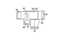
- FIG. 3 is an explanatory plan view for explaining the positional relationship between a first photodiode and a second photodiode that constitute the semiconductor device shown in FIG. 1.
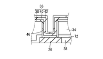
- FIG. 4 is an enlarged cross-sectional view of a second photodiode constituting the semiconductor device shown in FIG. 1.
- FIG. 2 is an equivalent circuit diagram when the semiconductor device shown in FIG. 1 is used as an optical sensor unit of a liquid crystal display device.
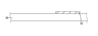
- FIG. 2 is a cross-sectional view for explaining a manufacturing process of the semiconductor device shown in FIG. 1 and showing a state where a light shielding layer is formed on a substrate.
- FIG. 3 is an explanatory plan view for explaining the positional relationship between a first photodiode and a second photodiode that constitute the semiconductor device shown in FIG. 1.
- FIG. 4 is an enlarged cross-sectional view of a
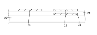
- FIG. 2 is a cross-sectional view for explaining a manufacturing process of the semiconductor device shown in FIG. 1, showing a state where a first semiconductor layer and a transistor semiconductor film are formed on a base layer.
- FIG. 2 is a cross-sectional view for explaining a manufacturing process of the semiconductor device shown in FIG. 1 and showing a state in which a gate electrode is formed on a gate insulating film.
- FIG. 2 is a cross-sectional view for explaining a manufacturing process of the semiconductor device shown in FIG. 1 and showing a state in which an n-type impurity is implanted.
- FIG. 2 is a cross-sectional view for explaining a manufacturing process of the semiconductor device shown in FIG. 1 and shows a state in which p-type impurities are implanted.
- FIG. 1 is a cross-sectional view for explaining a manufacturing process of the semiconductor device shown in FIG. 1, showing a state in which p-type impurities are implanted.
- FIG. 2 is a cross-sectional view for explaining a manufacturing process of the semiconductor device shown in FIG. 1 and showing a state in which a contact hole is formed in an interlayer insulating film.
- FIG. 4 is a cross-sectional view for explaining a manufacturing process of the semiconductor device shown in FIG. 1 and showing a state in which a second semiconductor layer is formed.
- FIG. 2 is a cross-sectional view for explaining a manufacturing process of the semiconductor device shown in FIG. 1 and showing a state in which electrodes / wirings are formed.
- FIG. 2 is a cross-sectional view for explaining a manufacturing process of the semiconductor device shown in FIG. 1 and showing a state in which a contact hole is formed in a planarization film.
- Sectional drawing which shows schematic structure of the semiconductor device as 2nd embodiment of this invention Sectional drawing which shows schematic structure of the semiconductor device as 3rd embodiment of this invention. Sectional drawing which shows schematic structure of the semiconductor device as 4th embodiment of this invention. Sectional drawing which shows schematic structure of the semiconductor device as 5th embodiment of this invention. Sectional drawing which shows schematic structure of the semiconductor device as 6th Embodiment of this invention.
- An optical sensor includes a first photodiode that is formed on a substrate and includes a diode semiconductor film having an n-type region, an intrinsic region, and a p-type region, and the diode semiconductor film. And a second photodiode connected to the first photodiode in parallel, and including a semiconductor layer having an intrinsic layer and at least one of an n-type layer and a p-type layer.
- One of the intrinsic region and the intrinsic layer is made of crystalline silicon, and the other of the intrinsic region and the intrinsic layer is made of amorphous silicon (first configuration relating to an optical sensor).
- one of the intrinsic region and the intrinsic layer is formed of amorphous silicon having a light detection sensitivity in the visible light region that is superior to that of crystalline silicon.
- the other of the intrinsic region and the intrinsic layer is formed of crystalline silicon, which has a light detection sensitivity in a wavelength region other than the visible light region, which is superior to that of amorphous silicon.
- the light detection sensitivity in the wavelength region other than the visible light region can be improved.
- the light detection sensitivity can be improved over a wide wavelength range including the visible light range.
- a second configuration related to the optical sensor is a configuration in which the semiconductor film for diode is formed of the crystalline silicon in the first configuration related to the optical sensor.
- the manufacturing process of the first photodiode can be simplified as compared with the case where only the intrinsic region is formed of crystalline silicon.
- a third configuration related to the optical sensor is a configuration in which the semiconductor layer includes the p-type layer, the intrinsic layer, and the n-type layer in the first or second configuration related to the optical sensor. .
- the second photodiode can be configured only by the semiconductor layer.
- a fourth configuration related to an optical sensor is the first or second configuration related to the optical sensor, wherein the semiconductor layer is formed on the n-type region, and the intrinsic layer is formed on the intrinsic layer.
- This is a configuration having a p-type layer.
- the n-type region of the first photodiode also serves as a part of the second photodiode (n + region doped with n-type impurities). As a result, the manufacturing process of the second photodiode can be simplified.
- a fifth configuration related to an optical sensor is the same as the first or second configuration related to the optical sensor, wherein the semiconductor layer is formed on the p-type region and the intrinsic layer is formed on the intrinsic layer.
- This is a configuration having an n-type layer.
- the p-type region of the first photodiode also serves as a part of the second photodiode (p + region doped with p-type impurities). As a result, the manufacturing process of the second photodiode can be simplified.
- a sixth configuration related to the optical sensor is a configuration in which the intrinsic layer has a thickness of 100 nm to 800 nm in any one of the first to fifth configurations related to the optical sensor. In such a configuration, it is possible to prevent the intrinsic layer from peeling off while improving the light detection sensitivity of the second photodiode.
- a seventh configuration related to the optical sensor further includes an interlayer insulating film formed so as to cover the semiconductor film for diodes in any one of the first to sixth configurations related to the optical sensor, and the interlayer insulating film
- the semiconductor layer is formed on a contact hole formed so as to penetrate the interlayer insulating film in the thickness direction, and the semiconductor layer and the diode semiconductor are formed in the contact hole.
- the membrane is in contact.
- the light receiving area of the second photodiode can be increased. As a result, it is possible to improve the light detection sensitivity of the second photodiode.
- the eighth configuration related to the optical sensor is a configuration in which the semiconductor layer is in contact with only one of the n-type region and the p-type region in the seventh configuration related to the optical sensor.
- the light receiving area of the first photodiode can be secured while the light receiving area of the second photodiode is secured.
- a semiconductor device includes a photosensor according to the embodiment of the present invention, a semiconductor film for a transistor formed on the substrate and having a channel region, a source region, and a drain region, A thin film transistor having a gate electrode for controlling the conductivity of the channel region and a gate insulating film provided between the gate electrode and the transistor semiconductor film is provided (first configuration relating to a semiconductor device).
- the semiconductor device In the first configuration relating to the semiconductor device, it is possible to realize a semiconductor device including an optical sensor having excellent light detection sensitivity.
- a second configuration related to the semiconductor device is a configuration in which the diode semiconductor film and the transistor semiconductor film are each formed of the crystalline silicon in the first configuration related to the semiconductor device.
- the semiconductor film for diode and the semiconductor film for transistor can be formed in the same manufacturing process. As a result, the manufacturing process of the semiconductor device can be simplified.
- a third configuration related to a semiconductor device is the first or second configuration related to the semiconductor device, further comprising a base layer on the substrate for preventing impurity diffusion from the substrate,
- the transistor semiconductor film is formed on the base layer.
- the semiconductor film for diode and the semiconductor film for transistor can be formed in the same manufacturing process. As a result, the manufacturing process of the semiconductor device can be simplified.
- the thickness of the semiconductor film for diode and the thickness of the semiconductor film for transistor are the same.
- the semiconductor film for diode and the semiconductor film for transistor can be formed in the same manufacturing process.
- the manufacturing process of the semiconductor device can be simplified. Note that the thickness of the semiconductor film for the diode and the thickness of the semiconductor film for the transistor do not have to be completely the same, and may be substantially the same.
- each figure referred below demonstrates the simplified main component required in order to demonstrate this invention among the structural members of embodiment of this invention for convenience of explanation. Therefore, the optical sensor and the semiconductor device according to the present invention can include arbitrary constituent members not shown in the drawings referred to in this specification. Moreover, the dimension of the member in each figure does not represent the dimension of an actual structural member, the dimension ratio of each member, etc. faithfully.
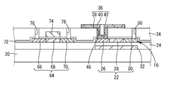
- FIG. 1 shows a semiconductor device 10 as a first embodiment of the present invention relating to a semiconductor device.
- the semiconductor device 10 includes an optical sensor 12 as a first embodiment of the present invention relating to an optical sensor, and a thin film transistor 14.
- the optical sensor 12 includes a first photodiode 16 and a second photodiode 18.
- the first photodiode 16 includes a diode semiconductor film 22 formed on the substrate 20.
- a substrate 20 a low alkali glass substrate or a quartz substrate can be adopted.
- the semiconductor film 22 for a diode is formed on the substrate 20 through the base layer 24 formed on the substrate 20.
- the underlayer 24 is provided to prevent impurity diffusion from the substrate 20.
- a silicon oxide film can be employed as the underlayer 24, a silicon oxide film can be employed.
- the thickness of the underlayer 24 is preferably 100 to 600 nm, more preferably 150 to 450 nm.
- the diode semiconductor film 22 is made of crystalline silicon. As crystalline silicon, low-temperature polysilicon, high-temperature polysilicon, continuous grain boundary silicon, microcrystalline silicon, or the like can be used.
- the diode semiconductor film 22 has a thickness of 25 to 100 nm.
- the first photodiode 16 is a so-called lateral structure PIN diode.
- n-type region 26 is formed so as to protrude to one side in the width direction of the diode semiconductor film 22 (direction perpendicular to the paper surface in FIG. 1). .
- a light shielding layer 32 formed on the substrate 20 and covered with the base layer 24 is provided below the first photodiode 16 (diode semiconductor film 22). This prevents light from entering the diode semiconductor film 22 from the side opposite to the side where the first photodiode 16 is provided through the substrate 20.
- the light shielding layer 32 is made of a metal material or the like. Considering the manufacturing method of the semiconductor device 10, it is desirable that the light shielding layer 32 be formed of Ta, W, Mo, or the like, which is a refractory metal.
- the light shielding layer 32 has a thickness of 200 to 300 nm.
- An interlayer insulating film 34 is formed on the substrate 20 so as to cover the first photodiode 16 (diode semiconductor film 22).
- the interlayer insulating film 34 for example, a silicon nitride film and a silicon oxide film formed in this order can be employed.
- a gate insulating film 72 described later is formed on the base layer 24 so as to cover the diode semiconductor film 22.
- An interlayer insulating film 34 is formed on the substrate 20 via the gate insulating film 72 and the base layer 24.
- the second photodiode 18 On the interlayer insulating film 34, the second photodiode 18 is provided.
- the second photodiode 18 includes a semiconductor layer 36.
- the semiconductor layer 36 is formed by laminating an n-type layer 38, an intrinsic layer 40, and a p-type layer 42 in this order.
- the second photodiode 18 is a so-called stacked structure PIN diode.
- the n-type layer 38, the intrinsic layer 40, and the p-type layer 42 are all made of amorphous silicon.
- the thickness of the n-type layer 38 is set to 20 to 100 nm due to film peeling and processing time.
- the thickness of the intrinsic layer 40 is set to 100 to 800 nm in order to allow the intrinsic layer 40 to absorb light and to prevent the intrinsic layer 40 from peeling off from the n-type layer 38.
- the thickness of the p-type layer 42 is set to 20 to 100 nm in view of film peeling and processing time.
- the lengthwise dimension of the semiconductor layer 36 is substantially the same as the lengthwise dimension of the diode semiconductor film 22 (dimension in the left-right direction in FIG. 2).
- the width direction dimension (the vertical dimension in FIG. 2) of the semiconductor layer 36 is slightly shorter than the width direction dimension (the vertical dimension in FIG. 2) of the diode semiconductor film 22.
- Such a semiconductor layer 36 is formed on the interlayer insulating film 34 such that the length direction thereof coincides with the length direction of the semiconductor film 22 for diode.
- the semiconductor layer 36 extends with a substantially constant width dimension in the direction in which the three regions (the n-type region 26, the intrinsic region 28, and the p-type region 30) formed in the diode semiconductor film 22 are arranged. , Formed on the interlayer insulating film 34.
- the semiconductor layer 36 thus formed on the interlayer insulating film 34 overlaps the diode semiconductor film 22 in the projection in the thickness direction of the substrate 20.
- 2/3 or more of the semiconductor layer 36 overlaps with the diode semiconductor film 22.
- the semiconductor layer 36 is formed on one side in the length direction of the diode semiconductor film 22 (on the n-type region 26 side) from the position where the entire semiconductor layer 36 overlaps the diode semiconductor film 22 in the projection in the thickness direction of the substrate 20. Has been. Thereby, the semiconductor layer 36 overlaps the vicinity of the boundary with the intrinsic region 28 in the p-type region 30 and the intrinsic region 28 and the n-type region 26 when viewed from the thickness direction of the substrate 20. In the projection in the thickness direction of the substrate 20, substantially the entire intrinsic region 28 overlaps the semiconductor layer 36.
- An electrode / wiring 44 is formed on a portion of the semiconductor layer 36 that does not overlap the diode semiconductor film 22 when viewed from the thickness direction of the substrate 20. Thereby, the p-type layer 42 and the electrode / wiring 44 are connected.
- the electrode / wiring 44 for example, one having a two-layer structure of a titanium nitride film and an aluminum film can be employed.
- a contact hole 46 is formed in the interlayer insulating film 34 and the gate insulating film 72 at a position overlapping with both the n-type region 26 and the semiconductor layer 36 in the projection in the thickness direction of the substrate 20.
- the semiconductor layer 36 penetrates into the contact hole 46.
- the inner peripheral surface and bottom surface of the contact hole 46 (the portion exposed through the contact hole 46 in the n-type region 26) is covered with the semiconductor layer 36.
- the n-type layer 38 is in contact with the n-type region 26 in the contact hole 46.
- the interlayer insulating film 34 and the gate insulating film 72 have a contact penetrating the interlayer insulating film 34 and the gate insulating film 72 in the thickness direction.
- Holes 48 and 50 are formed.
- the contact hole 48 is formed at a position overlapping the portion of the n-type region 26 that protrudes to one side in the width direction of the diode semiconductor film 22 in the projection in the thickness direction of the substrate 20.
- the contact hole 50 is formed at a position outside the one end in the length direction of the semiconductor layer 36 and overlapping the p-type region 30 in the projection in the thickness direction of the substrate 20.
- the electrodes / wirings 52 and 54 formed on the interlayer insulating film 34 are connected to the n-type region 26 and the p-type region 28, respectively.
- the electrodes / wirings 52 and 54 are made of the same material as the electrodes / wirings 44 formed on the semiconductor layer 36 (p-type layer 42).
- a planarizing film 56 is formed on the interlayer insulating film 34 so as to cover the semiconductor layer 36 and the electrodes / wirings 44, 52, 54.
- a silicon oxide film can be employed as the planarization film 56.
- the thickness of the planarizing film 56 is set to 1000 to 4000 nm.
- planarizing film 56 contact holes 58 and 60 penetrating the planarizing film 56 in the thickness direction are formed. As a result, the electrodes / wirings 44 and 54 and the electrodes / wirings 62 formed on the planarizing film 56 are connected. As the electrode / wiring 62, an indium tin oxide (ITO) film can be employed.
- ITO indium tin oxide
- the thin film transistor 14 includes a transistor semiconductor film 64 formed on the substrate 20 with the base layer 24 interposed therebetween.
- the transistor semiconductor film 64 is made of crystalline silicon. As crystalline silicon, low-temperature polysilicon, high-temperature polysilicon, continuous grain boundary silicon, microcrystalline silicon, or the like can be used.
- the crystalline silicon forming the transistor semiconductor film 64 may be the same as or different from the crystalline silicon forming the diode semiconductor film 22. In order to meet the device characteristics required for each of the optical sensor 12 and the thin film transistor 14, the crystalline silicon forming the diode semiconductor film 22 and the crystalline silicon forming the transistor semiconductor film 64 may be different. As a method for differentiating the crystalline silicon forming the diode semiconductor film 22 and the crystalline silicon forming the transistor semiconductor film 64, for example, an amorphous silicon film is irradiated with a laser, and then the diode semiconductor film 22 or transistor transistor is used.
- a catalytic element that promotes crystallization of the amorphous silicon film is applied to a region that later becomes the diode semiconductor film 22 and a region that becomes the transistor semiconductor film 64 in the amorphous silicon film.
- a method of irradiating the amorphous silicon film with a laser or the like can be employed.
- the crystalline silicon forming the transistor semiconductor film 64 and the crystalline silicon forming the diode semiconductor film 22 are the same.
- the thickness of the transistor semiconductor film 64 is substantially the same as the thickness of the diode semiconductor film 22.
- a source region 66, a channel region 68, and a drain region 70 are formed in this order along the base layer 24.
- the thin film transistor 14 includes a gate insulating film 72 formed on the base layer 24 so as to cover the transistor semiconductor film 64.
- the gate insulating film 72 covers not only the transistor semiconductor film 64 but also the diode semiconductor film 22.
- As the gate insulating film 72 a silicon oxide film can be employed.
- the gate insulating film 72 has a thickness of 20 to 150 nm.
- the thin film transistor 14 includes a gate electrode 74 formed on the gate insulating film 72.
- the gate electrode 74 is formed at a position covering the channel region 68 in the projection in the thickness direction of the substrate 20. By applying a gate voltage to the gate electrode 74, the source region 66 and the drain region 70 are connected.
- the gate electrode 74 is made of W, Ta, Ti, Mo, which is a refractory metal, or an alloy material of these refractory metals.
- the gate electrode 74 has a thickness of 300 to 600 nm.
- the gate electrode 74 is covered with an interlayer insulating film 34 formed on the gate insulating film 72.
- interlayer insulating film 34 contact holes 76 and 78 penetrating the interlayer insulating film 34 in the thickness direction are formed.
- the contact hole 76 is formed at a position overlapping the source region 66 in the projection in the thickness direction of the substrate 20.
- the contact hole 78 is formed at a position overlapping the drain region 70 in the projection in the thickness direction of the substrate 20.
- the electrodes / wirings 80 and 82 are made of the same material as the electrodes / wirings 44 formed on the semiconductor layer 36.
- the electrodes / wirings 80 and 82 are covered with a planarizing film 56.
- Such a semiconductor device 10 can be used as an optical sensor unit of a liquid crystal display device having a touch sensor function.
- FIG. 4 shows an equivalent circuit diagram when the semiconductor device 10 is used for an optical sensor unit.
- the optical sensor unit includes a first photodiode 16, a second photodiode 18, a capacitor 84, and a thin film transistor 14.
- a wiring for supplying a reset signal is connected to the p-type region 30 of the first photodiode 16 and the p-type layer 42 of the second photodiode, respectively.
- One electrode of the capacitor 84 and the gate electrode 74 of the thin film transistor 14 are connected to the n-type region 26 of the first photodiode 16 and the n-type layer 38 of the second photodiode 18, respectively.
- a wiring for supplying a read signal is connected to the other electrode of the capacitor 84.
- a wiring for supplying a constant voltage is connected to the source region 66 of the thin film transistor 14.
- Sensor circuit output data of the optical sensor unit is output from the drain region 70 of the thin film transistor 14.
- a reset signal and a readout signal are supplied at predetermined timings, so that the sensor circuit output corresponding to the amount of light received by the first photodiode 16 and the second photodiode 18 is obtained. Data can be obtained.
- the read signal is set to a high level. Thereby, the reading period starts. During the reading period, the reset signal is at a low level.
- the potential of the storage node 86 is pulled up via the capacitor 84 while the read signal is at a high level.
- the thin film transistor 14 is turned on and sensor circuit output data is output.
- the storage node 86 is a connection point between the capacitor 84, the n-type region 26 of the first photodiode 16, the n-type layer 38 of the second photodiode 18, and the gate electrode 74 of the thin film transistor 14. .
- the reading period ends when the reading signal is set to low level.
- the reset signal is set to high level. Thereby, a reset period is started.
- the read signal is at a low level.
- the reset period ends by setting the reset signal to low level.
- the sensing period starts.
- the readout signal is at a low level.
- the manufacturing method of the semiconductor device 10 is not limited to the manufacturing method described below.
- the light shielding layer 32 is formed at a predetermined position on the substrate 20. Specifically, first, a metal film that will later become the light shielding layer 32 is formed on the entire upper surface of the substrate 20 by sputtering. Thereafter, this metal film is patterned by photolithography. Thereby, as shown in FIG. 5A, the light shielding layer 32 is formed at a predetermined position on the substrate 20.
- the base layer 24 is formed on the upper side of the substrate 20 by CVD (Chemical Vapor Deposition). As a result, the light shielding layer 32 and the region not covered with the light shielding layer 32 on the upper surface of the substrate 20 are covered with the base layer 24.
- CVD Chemical Vapor Deposition
- the diode semiconductor film 22 and the transistor semiconductor film 64 are formed on the base layer 24. Specifically, first, an amorphous silicon film is formed on the entire upper surface of the base layer 24 by plasma CVD, sputtering, or the like. Subsequently, excimer laser is irradiated to the amorphous silicon film. As a result, a polysilicon film covering the entire top surface of the foundation layer 24 is formed. Thereafter, the polysilicon film is patterned by photolithography. As a result, as shown in FIG. 5B, the diode semiconductor film 22 and the transistor semiconductor film 64 are formed at predetermined positions on the base layer 24.
- the gate insulating film 72 is formed on the upper side of the substrate 20 by plasma CVD or the like. As a result, the diode semiconductor film 22, the transistor semiconductor film 64, and the region of the base layer 24 not covered with the diode semiconductor film 22 or the transistor semiconductor film 64 are covered with the gate insulating film 72.
- a gate electrode 74 is formed on the gate insulating film 72. Specifically, first, a conductive film that will later become the gate electrode 74 is formed on the entire upper surface of the gate insulating film 72 by sputtering or CVD. Thereafter, this conductive film is patterned by photolithography. As a result, the gate electrode 74 is formed at a predetermined position on the gate insulating film 72 as shown in FIG. 5C.
- an n-type impurity such as phosphorus is implanted into the diode semiconductor film 22 and the transistor semiconductor film 64.
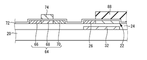
- a mask 88 made of a resist is formed on the gate insulating film 72 so as to cover a part of the semiconductor film for diode 22.
- n-type impurities such as phosphorus are ion-doped.
- an n-type impurity is implanted into a region of the diode semiconductor film 22 that is not covered with the mask 88 and a region of the transistor semiconductor film 64 that is not covered with the gate electrode 74.
- an n-type region 26 is formed in the diode semiconductor film 22.
- a source region 66 and a drain region 70 are formed in the transistor semiconductor film 64.
- a region where the n-type impurity is not implanted in the transistor semiconductor film 64 is a channel region 68 formed of an intrinsic semiconductor.
- p-type impurities such as boron are implanted into the semiconductor film for diode 22.
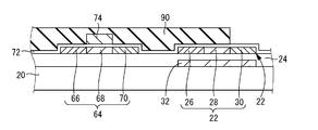
- a mask 90 made of resist is applied to the gate insulating film 72 so as to cover a part of the semiconductor film for diode 22 and the entire semiconductor film for transistor 64. Form on top.
- p-type impurities such as boron are ion-doped.
- the p-type impurity is implanted into a region of the diode semiconductor film 22 that is not covered with the mask 90.
- the p-type region 30 is formed in the diode semiconductor film 22.
- a region where neither n-type impurity nor p-type impurity is implanted in the diode semiconductor film 22 becomes an intrinsic region 28 formed of an intrinsic semiconductor.
- the impurities implanted into the diode semiconductor film 22 and the transistor semiconductor film 64 are activated. Specifically, heat treatment by RTA (Rapid Thermal Annealing) is performed in an inert atmosphere. As a result, in the n-type region 26 and the p-type region 30 of the diode semiconductor film 22 and the source region 66 and the drain region 70 of the transistor semiconductor film 64, doping damage such as crystal defects generated during ion doping is caused. It recovers and the implanted impurities are activated.
- RTA Rapid Thermal Annealing
- an interlayer insulating film 34 is formed on the upper side of the substrate 20 by plasma CVD or the like.
- the gate electrode 74 and the region of the gate insulating film 72 not covered with the gate electrode 74 are covered with the interlayer insulating film 34.
- contact holes 46 that penetrate the interlayer insulating film 34 and the gate insulating film 72 in the thickness direction, 48, 50, 76, 78 are formed.
- the contact holes 46, 48, 50, 76, 78 are formed by photolithography.
- the semiconductor layer 36 is formed. Specifically, first, an n-type semiconductor film that will later become the n-type layer 38 is formed on the upper side of the substrate 20 by plasma CVD. As a result, the upper surface of the interlayer insulating film 34 and the inside of the contact holes 46, 48, 50, 76, 78 are covered with the n-type semiconductor film.
- the n-type semiconductor film is an amorphous silicon film doped with n-type impurities.
- a source gas for forming the n-type semiconductor film by CVD for example, silane gas and hydrogen gas can be employed.
- phosphine can be employed as a doping gas for forming the n-type semiconductor film by CVD.
- an intrinsic semiconductor film that will later become the intrinsic layer 40 is formed on the n-type semiconductor film by plasma CVD. Thereby, the entire upper surface of the n-type semiconductor film is covered with the intrinsic semiconductor film.
- the intrinsic semiconductor film is an amorphous silicon film formed of an intrinsic semiconductor.
- silane gas and hydrogen gas can be employed as the source gas for forming the intrinsic semiconductor film by CVD.
- a p-type semiconductor film that will later become the p-type layer 42 is formed on the intrinsic semiconductor film by plasma CVD. Thereby, the entire upper surface of the intrinsic semiconductor film is covered with the p-type semiconductor film.
- the p-type semiconductor film is an amorphous silicon film doped with p-type impurities.
- a source gas for forming the p-type semiconductor film by CVD for example, silane gas and hydrogen gas can be employed.
- diborane can be used as a doping gas for forming the p-type semiconductor film by CVD.
- the target semiconductor layer 36 is formed.
- electrodes / wirings 52, 54, 80, 82 are formed on the interlayer insulating film 34, and electrodes / wirings 44 are formed on the semiconductor layer 36.
- a conductive film that will later become electrodes / wirings 44, 52, 54, 80, and 82 is formed on the upper side of the substrate 20 by sputtering, CVD, or the like.
- the semiconductor layer 36, the region not covered with the semiconductor layer 36 on the upper surface of the interlayer insulating film 34, and the inside of the contact holes 48, 50, 76, 78 are covered with the conductive film.
- the conductive film is patterned by photolithography.
- the electrodes / wirings 52, 54, 80, 82 are formed on the interlayer insulating film 34, and the electrodes / wiring 44 are formed on the semiconductor layer 36.
- a planarizing film 56 is formed on the upper side of the substrate 20 by plasma CVD or the like.
- the electrodes / wirings 44, 52, 54, 80, 82, the semiconductor layer 36, and the region not covered with the electrode wirings 44, 52, 54, 80, 82 and the semiconductor layer 36 in the interlayer insulating film 34 are formed.
- the flattening film 56 is covered.
- contact holes 58 and 60 penetrating through the planarizing film 56 in the thickness direction are formed on the planarizing film 56 thus formed.
- the contact holes 58 and 60 are formed by photolithography.
- an electrode / wiring 62 is formed on the planarizing film 56.
- a conductive film to be an electrode / wiring 62 later is formed on the entire upper surface of the planarizing film 56 by sputtering. Thereby, the entire upper surface of the planarizing film 56 is covered with the conductive film. Thereafter, the conductive film is patterned by photolithography. As a result, the electrode / wiring 62 is formed at a predetermined position on the flat film 56.
- the target semiconductor device 10 is obtained by such a manufacturing method.
- the intrinsic region 28 of the first photodiode 16 is formed of polysilicon
- the intrinsic layer 40 of the second photodiode 18 is formed of amorphous silicon.
- amorphous silicon has better light detection sensitivity than polysilicon
- polysilicon has better light detection sensitivity than amorphous silicon. Therefore, light in the visible light region is mainly absorbed by the intrinsic layer 40 of the second photodiode 18, and light in a wavelength region outside the visible light region is mainly absorbed in the intrinsic region 28 of the first photodiode 16. Absorbed.
- the light detection sensitivity of the optical sensor 12 can be improved over a wide wavelength range including the visible light region.
- the first photodiode 16 is provided with a region (intrinsic region 28) formed of an intrinsic semiconductor. As a result, the light detection sensitivity of the first photodiode 16 can be improved.
- the second photodiode 18 is provided with a layer (intrinsic layer 40) formed of an intrinsic semiconductor. As a result, the light detection sensitivity of the second photodiode 18 can be improved.
- the semiconductor layer 36 has a structure in which an n-type layer 38, an intrinsic layer 40, and a p-type layer 42 are stacked on the interlayer insulating film 34. Thereby, the light receiving area of the second photodiode 18 can be increased. As a result, the light detection sensitivity of the second photodiode 18 can be further improved.
- the semiconductor layer 36 overlaps the semiconductor film 22 for diode. Thereby, in the projection in the thickness direction of the substrate 20, the ratio of the optical sensor 12 to the substrate 20 can be reduced.
- the semiconductor layer 36 overlaps the diode semiconductor film 22 when viewed from the thickness direction of the substrate 20. Therefore, the ratio of the optical sensor 12 to the substrate 20 in the projection in the thickness direction of the substrate 20 can be further reduced.
- the n-type layer 38 is in contact only with the n-type region 26. Therefore, it is possible to avoid the absorption of incident light by the intrinsic region 28 from being hindered by the semiconductor layer 36.
- a contact hole 46 for contacting the n-type layer 38 and the n-type region 26 is formed in the interlayer insulating film 34 in the same process as the other contact holes 48, 50, 76, 78. Therefore, the number of steps necessary for manufacturing the semiconductor device 10 can be reduced.
- the semiconductor layer 36 As a method for forming the semiconductor layer 36, plasma CVD and photolithography are employed. Therefore, the number of steps necessary for manufacturing the semiconductor device 10 can be reduced.
- the semiconductor layer 36 is formed. As a result, the crystal states of the diode semiconductor film 22 and the semiconductor layer 36 can be easily changed.
- the diode semiconductor film 22 is formed of crystalline silicon. Therefore, it is easier to form the diode semiconductor film 22 than when only the intrinsic region 28 is formed of crystalline silicon.
- the diode semiconductor film 22 and the transistor semiconductor film 64 are formed in the same process. Therefore, the manufacturing process of the semiconductor device 10 can be simplified.
- the intrinsic layer 40 made of amorphous silicon is located above the intrinsic region 28 made of crystalline silicon. Therefore, as compared with the case where the intrinsic layer formed of crystalline silicon is located above the intrinsic region formed of amorphous silicon, the semiconductor layer 36 becomes an obstacle when detecting visible light. Can be avoided.
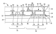
- the semiconductor device 92 of the present embodiment includes an optical sensor 94 according to the second embodiment of the present invention related to the optical sensor, instead of the optical sensor 12, as compared with the semiconductor device 10 of the first embodiment. .
- the optical sensor 94 is different in the semiconductor layer 96 from the optical sensor 12 of the first embodiment.
- the semiconductor layer 96 is obtained by sequentially stacking the intrinsic layer 40 and the p-type layer 42 on the n-type region 26 of the diode semiconductor film 22. That is, the second photodiode 98 in this embodiment includes the n-type region 26, the intrinsic layer 40, and the p-type layer 42.
- the semiconductor layer 96 can be formed as follows. First, an intrinsic semiconductor film that will later become the intrinsic layer 40 is formed on the upper side of the substrate 20 by plasma CVD. As a result, the upper surface of the interlayer insulating film 34 and the inside of the contact holes 46, 48, 50, 76, 78 are covered with the intrinsic semiconductor film.
- the intrinsic semiconductor film is an amorphous silicon film formed of an intrinsic semiconductor.
- silane gas and hydrogen gas can be employed as the source gas for forming the intrinsic semiconductor film by CVD.
- a p-type semiconductor film that will later become the p-type layer 42 is formed on the intrinsic semiconductor film by plasma CVD. Thereby, the entire upper surface of the intrinsic semiconductor film is covered with the p-type semiconductor film.
- the p-type semiconductor film is an amorphous silicon film doped with p-type impurities.
- a source gas for forming the p-type semiconductor film by CVD for example, silane gas and hydrogen gas can be employed.
- diborane can be used as a doping gas for forming the p-type semiconductor film by CVD.
- the n-type region 26 of the diode semiconductor film 22 serves as the n + region of the first photodiode 16 and the n + region of the second photodiode 98. Therefore, the number of steps required to form the semiconductor layer 96 can be reduced as compared with the semiconductor device 10 of the first embodiment.
- the semiconductor device 100 according to the present embodiment includes an optical sensor 102 according to the third embodiment of the present invention related to an optical sensor, instead of the optical sensor 12, as compared with the semiconductor device 10 according to the first embodiment. .
- This optical sensor 102 differs from the optical sensor 12 of the first embodiment in the formation positions of the semiconductor film 103 for the diode, the semiconductor layer 104, and the semiconductor layer 104.
- the positions of the n-type region 26 and the p-type region 30 are opposite to those of the diode semiconductor film 22 described in the first embodiment.
- the semiconductor layer 104 a p-type layer 42, an intrinsic layer 40, and an n-type layer 38 are sequentially formed on the p-type region 30 of the diode semiconductor film 22. That is, the second photodiode 106 in this embodiment includes the semiconductor layer 104.
- the semiconductor layer 104 can be formed as follows. First, a p-type semiconductor film that will later become the p-type layer 42 is formed on the upper side of the substrate 20 by plasma CVD. As a result, the upper surface of the interlayer insulating film 34 and the inside of the contact holes 46, 48, 50, 76, 78 are covered with the p-type semiconductor film.
- the p-type semiconductor film is an amorphous silicon film doped with p-type impurities.
- a source gas for forming the p-type semiconductor film by CVD for example, silane gas and hydrogen gas can be employed.
- diborane can be used as a doping gas for forming the p-type semiconductor film by CVD.
- an intrinsic semiconductor film that will later become the intrinsic layer 40 is formed on the p-type semiconductor film by plasma CVD. Thereby, the entire upper surface of the p-type semiconductor film is covered with the intrinsic semiconductor film.
- the intrinsic semiconductor film is an amorphous silicon film formed of an intrinsic semiconductor.
- silane gas and hydrogen gas can be employed as the source gas for forming the intrinsic semiconductor film by CVD.
- an n-type semiconductor film that will later become the n-type layer 38 is formed on the intrinsic semiconductor film by plasma CVD. Thereby, the entire upper surface of the intrinsic semiconductor film is covered with the n-type semiconductor film.
- the n-type semiconductor film is an amorphous silicon film doped with n-type impurities.
- a source gas for forming the n-type semiconductor film by CVD for example, silane gas and hydrogen gas can be employed.
- phosphine can be employed as a doping gas for forming the n-type semiconductor film by CVD.
- the target semiconductor layer 104 is formed as shown in FIG.
- the semiconductor device 108 of this embodiment includes an optical sensor 110 according to a fourth embodiment of the present invention relating to the optical sensor, instead of the optical sensor 12. .
- the photosensor 110 differs from the photosensor 12 of the first embodiment in the formation positions of the semiconductor film 111 for a diode, the semiconductor layer 112, and the semiconductor layer 112.
- the positions of the n-type region 26 and the p-type region 30 are opposite to those of the diode semiconductor film 22 described in the first embodiment.
- the semiconductor layer 112 is formed by sequentially forming the intrinsic layer 40 and the n-type layer 38 on the p-type region 30 of the diode semiconductor film 22. That is, the second photodiode 114 in this embodiment includes the p-type region 30, the intrinsic layer 40, and the n-type layer 38.
- the semiconductor layer 112 can be formed as follows. First, an intrinsic semiconductor film that will later become the intrinsic layer 40 is formed on the upper side of the substrate 20 by plasma CVD. As a result, the upper surface of the interlayer insulating film 34 and the inside of the contact holes 46, 48, 50, 76, 78 are covered with the intrinsic semiconductor film.
- the intrinsic semiconductor film is an amorphous silicon film formed of an intrinsic semiconductor.
- silane gas and hydrogen gas can be employed as the source gas for forming the intrinsic semiconductor film by CVD.
- a p-type semiconductor film that will later become the n-type layer 38 is formed on the intrinsic semiconductor film by plasma CVD. Thereby, the entire upper surface of the intrinsic semiconductor film is covered with the n-type semiconductor film.
- the n-type semiconductor film is an amorphous silicon film doped with n-type impurities.
- a source gas for forming the n-type semiconductor film by CVD for example, silane gas and hydrogen gas can be employed.
- phosphine can be employed as a doping gas for forming the n-type semiconductor film by CVD.
- the target semiconductor layer 112 is formed.
- the p-type region 30 of the diode semiconductor film 22 serves as both the p + region of the first photodiode 16 and the p + region of the second photodiode 114.
- the number of processes required in order to form the semiconductor layer 112 can be decreased.
- the semiconductor device 116 of this embodiment differs from the semiconductor device 10 of the first embodiment in the connection between the electrode / wiring 62 and the second photodiode 18.
- the electrode / wiring 44 is not formed on the semiconductor layer 36, and the electrode / wiring 62 and the semiconductor layer 36 (p-type layer 42) are directly connected. As a result, it is possible to avoid a problem caused by the formation of the electrode / wiring 44 on the semiconductor layer 36, that is, a problem that the light receiving area of the second photodiode 18 is reduced. As a result, the light detection sensitivity of the second photodiode 18 can be improved.
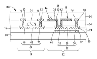
- the electrode / wiring 62 is not formed on the planarizing film 56 as compared with the semiconductor device 10 of the first embodiment.
- the p + region (p-type region 30) of the first photodiode 16 and the p + region (p-type layer 42) of the second photodiode 18 are connected without the electrode / wiring 62.
- the p + region (p-type region 30) of the first photodiode 16 and the p + region (p-type layer 42) of the second photodiode 18 can be connected only by a low resistance electrode / wiring. .
- the diode semiconductor film 22 may be formed of amorphous silicon, and the semiconductor layers 36, 96, 104, and 112 may be formed of crystalline silicon.
- the transistor semiconductor film 64 may be formed of amorphous silicon or crystalline silicon.
- a method of forming the diode semiconductor film 22 from amorphous silicon and forming the transistor semiconductor film 64 from crystalline silicon for example, in the amorphous silicon film formed on the base layer 24, the transistor semiconductor film 64 is formed later.
- a method of annealing the amorphous silicon film after introducing a catalyst element for promoting crystallization of amorphous silicon by ion implantation or the like can be employed.
- the intrinsic region 28 in the diode semiconductor film 22 may be formed from amorphous silicon, and the intrinsic layer 40 in the semiconductor layers 36, 96, 104, and 112 may be formed from crystalline silicon. good.
- a method of forming the intrinsic region 28 with amorphous silicon for example, in the amorphous silicon film formed on the underlayer 24, an amorphous region is formed into a region that later becomes the n-type region 26 and a region that becomes the p-type region 30.
- a method of annealing an amorphous silicon film after introducing a catalytic element for promoting crystallization of porous silicon by ion implantation or the like can be employed.
- a method of forming the intrinsic layer 40 from crystalline silicon a conventionally known method such as plasma CVD or sputtering can be employed.
- the layers 38, 40, 42 included in the semiconductor layers 36, 96, 104, 112 are formed of silicon carbide, silicon germanium, germanium, compound semiconductor, It may be formed of chalcogenide, polysilicon or the like.
- the n-type layer 38 and the p-type layer 42 may be formed by ion doping impurities into a semiconductor film formed by plasma CVD or the like.
- the semiconductor layers 36, 96, 104, and 112 do not necessarily need to overlap the intrinsic region 28 in the projection in the thickness direction of the substrate 20.
Landscapes
- Light Receiving Elements (AREA)
- Solid State Image Pick-Up Elements (AREA)
Abstract
可視光領域を含む幅広い波長域に亘って光検出感度を向上させることが出来る、新規な構造の光センサ及びこの光センサを備えた半導体装置を提供することを、目的とする。基板20上に形成されて、n型領域26と真性領域28とp型領域30を有するダイオード用半導体膜22を備える第一のフォトダイオード16と、ダイオード用半導体膜22上に形成されて、n型層38とp型層42の少なくとも一方と真性層40を有する半導体層36を含んで構成されると共に第一のフォトダイオード16と並列に接続される第二のフォトダイオード18とを、備えており、真性領域28と真性層40の一方が結晶質シリコンによって形成され、真性領域28と真性層40の他方が非晶質シリコンによって形成されている。
Description
本発明は、光センサ及び該光センサを備えた半導体装置に関する。
近年、特開2009-10125号公報(特許文献1)に記載されているように、薄膜ダイオードと薄膜トランジスタが同じ基板上に形成された半導体装置が知られている。このような半導体装置においては、製造工程の簡略化等の観点から、薄膜ダイオードや薄膜トランジスタの活性領域となる島状半導体層が基板上に形成された同一の結晶質ケイ素膜によって形成されている。
ところで、結晶質ケイ素膜を基板上に形成する方法としては、特許文献1にも記載されているように、基板上に形成された非晶質ケイ素膜にレーザー光を照射して非晶質ケイ素膜を結晶化させる方法が一般的に利用されている。それ故、照射するレーザー光の波長との関係上、非晶質ケイ素膜を薄くする必要がある。
しかしながら、非晶質ケイ素膜を薄くすると、非晶質ケイ素膜にレーザー光を照射することで形成される結晶質ケイ素膜や、当該結晶質ケイ素膜からなる島状半導体層が薄くなる。その結果、薄膜ダイオードの光検出感度が十分でないという問題があった。
本発明の目的は、可視光領域を含む幅広い波長域に亘って光検出感度を向上させることが出来る、新規な構造の光センサ及びこの光センサを備えた半導体装置を提供することである。
本発明の光センサは、基板上に形成されて、n型領域と真性領域とp型領域を有するダイオード用半導体膜を備える第一のフォトダイオードと、前記ダイオード用半導体膜上に形成されて、n型層とp型層の少なくとも一方と真性層を有する半導体層を含んで構成されると共に前記第一のフォトダイオードと並列に接続される第二のフォトダイオードとを、備えており、前記真性領域と前記真性層の一方が結晶質シリコンによって形成され、該真性領域と該真性層の他方が非晶質シリコンによって形成されている。
本発明の光センサによれば、可視光領域を含む幅広い波長域に亘って光検出感度を向上させることができる。
本発明の一実施形態に係る光センサは、基板上に形成されて、n型領域と真性領域とp型領域を有するダイオード用半導体膜を備える第一のフォトダイオードと、前記ダイオード用半導体膜上に形成されて、n型層とp型層の少なくとも一方と真性層を有する半導体層を含んで構成されると共に前記第一のフォトダイオードと並列に接続される第二のフォトダイオードとを、備えており、前記真性領域と前記真性層の一方が結晶質シリコンによって形成され、該真性領域と該真性層の他方が非晶質シリコンによって形成されている(光センサに関する第1の構成)。
光センサに関する第1の構成においては、可視光領域での光検出感度が結晶質シリコンよりも優れている非晶質シリコンによって、真性領域と真性層の一方が形成されている。これにより、第一のフォトダイオードと第二のフォトダイオードの一方において、可視光領域での光検出感度を向上させることができる。
また、可視光領域以外の波長域での光検出感度が非晶質シリコンよりも優れている結晶質シリコンによって、真性領域と真性層の他方が形成されている。これにより、第一のフォトダイオードと第二のフォトダイオードの他方において、可視光領域以外の波長域での光検出感度を向上させることができる。
従って、光センサに関する第1の構成においては、可視光領域を含む幅広い波長域に亘って光検出感度を向上させることができる。
光センサに関する第2の構成は、前記光センサに関する第1の構成において、前記ダイオード用半導体膜が前記結晶質シリコンによって形成されている構成である。このような構成においては、真性領域だけを結晶質シリコンによって形成する場合に比して、第一のフォトダイオードの製造工程の簡略化を図ることができる。
光センサに関する第3の構成は、前記光センサに関する第1又は第2の構成において、前記半導体層が、前記p型層と、前記真性層と、前記n型層を有している構成である。このような構成においては、半導体層だけで第二のフォトダイオードを構成することができる。
光センサに関する第4の構成は、前記光センサに関する第1又は第2の構成において、前記半導体層が、前記n型領域上に形成された前記真性層と、該真性層上に形成された前記p型層を有している構成である。このような構成においては、第一のフォトダイオードのn型領域が第二のフォトダイオードの一部(n型不純物がドーピングされたn+領域)を兼ねている。その結果、第二のフォトダイオードの製造工程の簡略化を図ることができる。
光センサに関する第5の構成は、前記光センサに関する第1又は第2の構成において、前記半導体層が、前記p型領域上に形成された前記真性層と、該真性層上に形成された前記n型層を有している構成である。このような構成においては、第一のフォトダイオードのp型領域が第二のフォトダイオードの一部(p型不純物がドーピングされたp+領域)を兼ねている。その結果、第二のフォトダイオードの製造工程の簡略化を図ることができる。
光センサに関する第6の構成は、前記光センサに関する第1~第5の構成の何れか一つにおいて、前記真性層の厚さが100nm~800nmとされている構成である。このような構成においては、第二のフォトダイオードの光検出感度を良好にしつつ、真性層が剥がれるのを防ぐことができる。
光センサに関する第7の構成は、前記光センサに関する第1~第6の構成の何れか一つにおいて、前記ダイオード用半導体膜を覆うように形成された層間絶縁膜を更に備え、前記層間絶縁膜上に前記半導体層が形成され、前記層間絶縁膜を厚さ方向に貫通するように形成されたコンタクトホール内に前記半導体層が入り込んでおり、前記コンタクトホール内において前記半導体層と前記ダイオード用半導体膜が接触している構成である。このような構成においては、第二のフォトダイオードの受光面積を大きくすることができる。その結果、第二のフォトダイオードの光検出感度を向上させることが可能となる。
光センサに関する第8の構成は、前記光センサに関する第7の構成において、前記半導体層が前記n型領域とp型領域の何れか一方だけに接触している構成である。このような構成においては、第二のフォトダイオードの受光面積を確保しつつ、第一のフォトダイオードの受光面積を確保することができる。その結果、第一のフォトダイオードと第二のフォトダイオードのそれぞれの光検出感度を向上させることが可能となる。
本発明の一実施形態に係る半導体装置は、前記本発明の一実施形態に係る光センサと、前記基板上に形成されて、チャネル領域、ソース領域及びドレイン領域を有するトランジスタ用半導体膜と、前記チャネル領域の導電性を制御するゲート電極と、該ゲート電極と前記トランジスタ用半導体膜の間に設けられたゲート絶縁膜とを有する薄膜トランジスタとを備えている(半導体装置に関する第1の構成)。
半導体装置に関する第1の構成においては、優れた光検出感度を有する光センサを備えた半導体装置を実現することができる。
半導体装置に関する第2の構成は、前記半導体装置に関する第1の構成において、前記ダイオード用半導体膜と前記トランジスタ用半導体膜が、それぞれ、前記結晶質シリコンによって形成されている構成である。このような構成においては、ダイオード用半導体膜とトランジスタ用半導体膜を同じ製造工程で形成することができる。その結果、半導体装置の製造工程の簡略化を図ることが可能となる。
半導体装置に関する第3の構成は、前記半導体装置に関する第1又は第2の構成において、前記基板上には、該基板からの不純物拡散を防ぐための下地層を更に備え、前記ダイオード用半導体膜と前記トランジスタ用半導体膜が前記下地層上に形成されている構成である。このような構成においては、ダイオード用半導体膜とトランジスタ用半導体膜を同じ製造工程で形成することができる。その結果、半導体装置の製造工程の簡略化を図ることが可能となる。
半導体装置に関する第4の構成は、前記半導体装置に関する第1~第3の構成の何れか一つにおいて、前記ダイオード用半導体膜の厚さと前記トランジスタ用半導体膜の厚さが同じである構成である。このような構成においては、ダイオード用半導体膜とトランジスタ用半導体膜を同じ製造工程で形成することができる。その結果、半導体装置の製造工程の簡略化を図ることが可能となる。なお、ダイオード用半導体膜の厚さとトランジスタ用半導体膜の厚さは完全に同じである必要はなく、実質的に同じであれば良い。
以下、本発明のより具体的な実施形態について、図面を参照しながら説明する。なお、以下で参照する各図は、説明の便宜上、本発明の実施形態の構成部材のうち、本発明を説明するために必要な主要部材のみを簡略化して示したものである。従って、本発明に係る光センサ及び半導体装置は、本明細書が参照する各図に示されていない任意の構成部材を備え得る。また、各図中の部材の寸法は、実際の構成部材の寸法および各部材の寸法比率等を忠実に表したものではない。
[第一の実施形態]
図1には、半導体装置に関する本発明の第一の実施形態としての半導体装置10が示されている。この半導体装置10は、光センサに関する本発明の第一の実施形態としての光センサ12と、薄膜トランジスタ14とを備えている。
図1には、半導体装置に関する本発明の第一の実施形態としての半導体装置10が示されている。この半導体装置10は、光センサに関する本発明の第一の実施形態としての光センサ12と、薄膜トランジスタ14とを備えている。
より詳細には、光センサ12は、第一のフォトダイオード16と、第二のフォトダイオード18とを備えている。
第一のフォトダイオード16は、基板20上に形成されたダイオード用半導体膜22を備えている。基板20としては、低アルカリガラス基板や石英基板を採用することができる。
本実施形態では、基板20上に形成された下地層24を介して、ダイオード用半導体膜22が基板20上に形成されている。下地層24は、基板20からの不純物拡散を防ぐために設けられている。下地層24としては、酸化シリコン膜を採用することができる。下地層24の厚さは、好ましくは100~600nm、より好ましくは150~450nmとされている。
ダイオード用半導体膜22は、結晶質シリコンによって形成されている。結晶質シリコンとしては、低温ポリシリコンや高温ポリシリコン,連続粒界シリコン,微結晶シリコン等を採用することができる。ダイオード用半導体膜22の厚さは、25~100nmとされている。
ダイオード用半導体膜22には、n型領域26と真性領域28とp型領域30とがこの順番で下地層24に沿って並ぶように形成されている。このことから明らかなように、第一のフォトダイオード16は所謂ラテラル構造のPINダイオードとされている。
なお、本実施形態では、図2に示されているように、n型領域26だけがダイオード用半導体膜22の幅方向(図1において紙面に垂直な方向)一方側へ突出して形成されている。
このような第一のフォトダイオード16(ダイオード用半導体膜22)の下方には、基板20上に形成されて且つ下地層24で覆われた遮光層32が設けられている。これにより、第一のフォトダイオード16が設けられた側とは反対側から、基板20を通過して、ダイオード用半導体膜22に光が入射するのを防止している。
遮光層32は、金属材料等によって形成されている。半導体装置10の製造方法を考慮すると、遮光層32は高融点金属であるTaやW,Mo等で形成されていることが望ましい。遮光層32の厚さは、200~300nmとされている。
第一のフォトダイオード16(ダイオード用半導体膜22)を覆うようにして、層間絶縁膜34が基板20上に形成されている。層間絶縁膜34としては、例えば、窒化シリコン膜と酸化シリコン膜がこの順番で形成されたもの等を採用することができる。本実施形態では、後述するゲート絶縁膜72が、ダイオード用半導体膜22を覆うようにして、下地層24上に形成されている。そして、ゲート絶縁膜72と下地層24とを介して、層間絶縁膜34が基板20上に形成されている。
層間絶縁膜34上には、第二のフォトダイオード18が設けられている。第二のフォトダイオード18は、半導体層36を備えている。
半導体層36は、図3にも示されているように、n型層38と真性層40とp型層42とがこの順番で積層されたものである。このことから明らかなように、第二のフォトダイオード18は所謂積層構造のPINダイオードとされている。
n型層38、真性層40及びp型層42は、何れも、アモルファスシリコンによって形成されている。n型層38の厚さは、膜剥がれや処理時間の関係から、20~100nmとされている。真性層40の厚さは、真性層40による光の吸収を可能にすると共に真性層40がn型層38から剥がれるのを防止するために、100~800nmとされている。p型層42の厚さは、膜剥がれや処理時間の関係から、20~100nmとされている。
半導体層36の長さ方向寸法(図2の左右方向の寸法)は、ダイオード用半導体膜22の長さ方向寸法(図2の左右方向の寸法)と略同じとされている。半導体層36の幅方向寸法(図2の上下方向の寸法)は、ダイオード用半導体膜22の幅方向寸法(図2の上下方向の寸法)よりも僅かに短くされている。
このような半導体層36は、その長さ方向がダイオード用半導体膜22の長さ方向と一致するようにして、層間絶縁膜34上に形成されている。換言すれば、半導体層36は、ダイオード用半導体膜22に形成された三つの領域(n型領域26,真性領域28及びp型領域30)が並ぶ方向に略一定の幅寸法で延びるようにして、層間絶縁膜34上に形成されている。
このようにして層間絶縁膜34上に形成された半導体層36は、基板20の厚さ方向の投影において、ダイオード用半導体膜22と重なっている。基板20の厚さ方向の投影において、半導体層36の2/3以上がダイオード用半導体膜22と重なっている。
基板20の厚さ方向の投影において半導体層36の全体がダイオード用半導体膜22と重なる位置よりもダイオード用半導体膜22の長さ方向一方側(n型領域26側)に、半導体層36が形成されている。これにより、半導体層36は、基板20の厚さ方向から見た場合に、p型領域30における真性領域28との境界付近と真性領域28とn型領域26に重なっている。基板20の厚さ方向の投影において、真性領域28の略全体が半導体層36と重なっている。
半導体層36において基板20の厚さ方向から見た場合にダイオード用半導体膜22と重ならない部分の上には、電極・配線44が形成されている。これにより、p型層42と電極・配線44が接続されている。電極・配線44としては、例えば、窒化チタン膜とアルミニウム膜の二層構造を有するもの等を採用することができる。
層間絶縁膜34及びゲート絶縁膜72には、基板20の厚さ方向の投影において、n型領域26と半導体層36の両方に対して重なる位置にコンタクトホール46が形成されている。半導体層36は、コンタクトホール46内に入り込んでいる。これにより、コンタクトホール46の内周面と底面(n型領域26においてコンタクトホール46を通じて露出されている部分)が半導体層36で覆われている。このことから明らかなように、n型層38はコンタクトホール46内においてn型領域26と接触している。
層間絶縁膜34及びゲート絶縁膜72には、n型層38とn型領域26を接触させるためのコンタクトホール46以外にも、層間絶縁膜34及びゲート絶縁膜72を厚さ方向に貫通するコンタクトホール48,50が形成されている。コンタクトホール48は、基板20の厚さ方向の投影において、n型領域26においてダイオード用半導体膜22の幅方向一方側へ突出している部分と重なる位置に形成されている。コンタクトホール50は、基板20の厚さ方向の投影において、半導体層36の長さ方向一端よりも外側であって且つp型領域30と重なる位置に形成されている。このようにして、コンタクトホール48,50が形成されていることにより、n型領域26とp型領域28のそれぞれに対して、層間絶縁膜34上に形成された電極・配線52,54が接続されている。電極・配線52,54は、半導体層36(p型層42)上に形成された電極・配線44と同じ材料で形成されている。
半導体層36や電極・配線44,52,54を覆うようにして、平坦化膜56が層間絶縁膜34上に形成されている。平坦化膜56としては、酸化シリコン膜を採用することができる。平坦化膜56の厚さは、1000~4000nmとされている。
平坦化膜56には、平坦化膜56を厚さ方向に貫通するコンタクトホール58,60が形成されている。これにより、電極・配線44,54と平坦化膜56上に形成された電極・配線62が接続されている。電極・配線62としては、酸化インジウム錫(ITO)膜を採用することができる。
一方、薄膜トランジスタ14は、下地層24を介して基板20上に形成されたトランジスタ用半導体膜64を備えている。トランジスタ用半導体膜64は、結晶質シリコンによって形成されている。結晶質シリコンとしては、低温ポリシリコンや高温ポリシリコン,連続粒界シリコン,微結晶シリコン等を採用することができる。
トランジスタ用半導体膜64を形成する結晶質シリコンは、ダイオード用半導体膜22を形成する結晶質シリコンと同じであっても良いし、異なっていても良い。光センサ12と薄膜トランジスタ14のそれぞれにおいて要求されるデバイス特性に応じるために、ダイオード用半導体膜22を形成する結晶質シリコンとトランジスタ用半導体膜64を形成する結晶質シリコンを異ならせても良い。ダイオード用半導体膜22を形成する結晶質シリコンとトランジスタ用半導体膜64を形成する結晶質シリコンを異ならせる方法としては、例えば、アモルファスシリコン膜をレーザ照射して、後にダイオード用半導体膜22やトランジスタ用半導体膜64となるポリシリコン膜を形成する場合、アモルファスシリコンシリコン膜の結晶化を促進する触媒元素をアモルファスシリコン膜において後にダイオード用半導体膜22となる領域とトランジスタ用半導体膜64となる領域とに添加した後、アモルファスシリコン膜をレーザ照射する方法等を採用することができる。なお、本実施形態では、トランジスタ用半導体膜64を形成する結晶質シリコンとダイオード用半導体膜22を形成する結晶質シリコンは同じとされている。
トランジスタ用半導体膜64の厚さは、ダイオード用半導体膜22の厚さと略同じである。トランジスタ用半導体膜64には、ソース領域66とチャネル領域68とドレイン領域70とがこの順番で下地層24に沿って並ぶように形成されている。
薄膜トランジスタ14は、トランジスタ用半導体膜64を覆うようにして、下地層24上に形成されたゲート絶縁膜72を備えている。ゲート絶縁膜72は、トランジスタ用半導体膜64だけでなく、ダイオード用半導体膜22も覆っている。ゲート絶縁膜72としては、酸化シリコン膜を採用することができる。ゲート絶縁膜72の厚さは、20~150nmとされている。
薄膜トランジスタ14は、ゲート絶縁膜72上に形成されたゲート電極74を備えている。ゲート電極74は、基板20の厚さ方向の投影において、チャネル領域68を覆う位置に形成されている。ゲート電極74にゲート電圧を印加することによって、ソース領域66とドレイン領域70が接続されるようになっている。
ゲート電極74は、高融点金属であるWやTa,Ti,Mo或いはこれら高融点金属の合金材料によって形成されている。ゲート電極74の厚さは、300~600nmとされている。
ゲート電極74は、ゲート絶縁膜72上に形成された層間絶縁膜34によって覆われている。層間絶縁膜34には、層間絶縁膜34を厚さ方向に貫通するコンタクトホール76,78が形成されている。
コンタクトホール76は、基板20の厚さ方向の投影において、ソース領域66と重なる位置に形成されている。コンタクトホール78は、基板20の厚さ方向の投影において、ドレイン領域70と重なる位置に形成されている。このようにして、コンタクトホール76,78が形成されていることにより、ソース領域66とドレイン領域70のそれぞれに対して、層間絶縁膜34上に形成された電極・配線80,82が接続されている。
電極・配線80,82は、半導体層36上に形成された電極・配線44と同じ材料で形成されている。電極・配線80,82は、平坦化膜56によって覆われている。
このような半導体装置10は、タッチセンサ機能を有する液晶表示装置の光センサ部として用いることができる。半導体装置10を光センサ部に用いた場合の等価回路図を図4に示す。
光センサ部は、第一のフォトダイオード16と、第二のフォトダイオード18と、コンデンサ84と、薄膜トランジスタ14を備えている。第一のフォトダイオード16のp型領域30と第二のフォトダイオードのp型層42には、それぞれ、リセット信号を供給するための配線が接続されている。第一のフォトダイオード16のn型領域26と第二のフォトダイオード18のn型層38には、それぞれ、コンデンサ84の一方の電極と薄膜トランジスタ14のゲート電極74が接続されている。コンデンサ84の他方の電極には、読み出し信号を供給するための配線が接続されている。薄膜トランジスタ14のソース領域66には、定電圧を供給するための配線が接続されている。薄膜トランジスタ14のドレイン領域70から光センサ部のセンサ回路出力データが出力される。
このような光センサ部においては、リセット信号及び読み出し信号をそれぞれ所定のタイミングで供給することにより、第一のフォトダイオード16及び第二のフォトダイオード18で受光した光の量に応じたセンサ回路出力データを得ることができる。
具体的には、先ず、読み出し信号をハイレベルにする。これにより、読み出し期間が開始する。読み出し期間中、リセット信号はローレベルとされている。
読み出し信号がハイレベルの間、コンデンサ84を介して蓄積ノード86の電位がプルアップされる。プルアップされた蓄積ノード86の電位が薄膜トランジスタ14の閾値電圧を超えると、薄膜トランジスタ14がON状態となり、センサ回路出力データが出力される。なお、蓄積ノード86とは、コンデンサ84と、第一のフォトダイオード16のn型領域26と、第二のフォトダイオード18のn型層38と、薄膜トランジスタ14のゲート電極74との接続点である。
読み出し信号をローレベルにすることにより、読み出し期間が終了する。読み出し期間が終了したら、リセット信号をハイレベルにする。これにより、リセット期間が開始される。リセット期間中、読み出し信号はローレベルにされている。
リセット信号がハイレベルの間、第一のフォトダイオード16と第二のフォトダイオード18のそれぞれに順方向電流が流れる。その結果、蓄積ノード86の電位がリセットされる。
リセット信号をローレベルにすることにより、リセット期間が終了する。リセット期間が終了したら、センシング期間が開始される。センシング期間中、読み出し信号はローレベルにされている。
リセット信号をローレベルにすることにより、第一のフォトダイオード16と第二のフォトダイオード18のそれぞれに逆バイアスが発生する。そして、第一のフォトダイオード16と第二のフォトダイオード18のそれぞれに入射した光の量に応じて発生する光電流によって、蓄積ノード86の電位が変化する。
このような動作を繰り返すことにより、光センサ部からのセンサ回路出力データの読み出しを行うことができる。
続いて、上述の如き半導体装置10の製造方法について、説明する。なお、半導体装置10の製造方法は、以下に記載の製造方法に限定されない。
先ず、遮光層32を基板20上の所定位置に形成する。具体的には、先ず、後に遮光層32となる金属膜をスパッタによって基板20の上面全体に形成する。その後、この金属膜をフォトリソグラフィによってパターニングする。これにより、図5Aに示されているように、遮光層32が基板20上の所定位置に形成される。
次に、下地層24をCVD(Chemical Vapor Deposition)によって基板20の上側に形成する。これにより、遮光層32と、基板20の上面において遮光層32で覆われていない領域とが、下地層24で覆われる。
続いて、ダイオード用半導体膜22とトランジスタ用半導体膜64とを下地層24上に形成する。具体的には、先ず、アモルファスシリコン膜をプラズマCVDやスパッタ等によって下地層24の上面全体に形成する。続いて、アモルファスシリコン膜にエキシマレーザーを照射する。これにより、下地層24の上面全体を覆うポリシリコン膜が形成される。その後、ポリシリコン膜をフォトリソグラフィによってパターニングする。これにより、図5Bに示されているように、ダイオード用半導体膜22とトランジスタ用半導体膜64が下地層24上の所定位置に形成される。
次に、ゲート絶縁膜72をプラズマCVD等によって基板20の上側に形成する。これにより、ダイオード用半導体膜22と、トランジスタ用半導体膜64と、下地層24においてダイオード用半導体膜22やトランジスタ用半導体膜64で覆われていない領域とが、ゲート絶縁膜72で覆われる。
続いて、ゲート電極74をゲート絶縁膜72上に形成する。具体的には、先ず、後にゲート電極74となる導電膜をスパッタ又はCVD等によってゲート絶縁膜72の上面全体に形成する。その後、この導電膜をフォトリソグラフィによってパターニングする。これにより、図5Cに示されているように、ゲート電極74がゲート絶縁膜72上の所定位置に形成される。
次に、リン等のn型不純物をダイオード用半導体膜22とトランジスタ用半導体膜64とに注入する。具体的には、先ず、図5Dに示されているように、ダイオード用半導体膜22の一部を覆うようにして、レジストからなるマスク88をゲート絶縁膜72上に形成する。その後、リン等のn型不純物をイオンドーピングする。これにより、ダイオード用半導体膜22においてマスク88で覆われていない領域とトランジスタ用半導体膜64においてゲート電極74で覆われていない領域とにn型不純物が注入される。その結果、ダイオード用半導体膜22には、n型領域26が形成される。トランジスタ用半導体膜64には、ソース領域66とドレイン領域70とが形成される。トランジスタ用半導体膜64においてn型不純物が注入されていない領域は、真性半導体で形成されたチャネル領域68となる。ダイオード用半導体膜22及びトランジスタ用半導体膜64へのn型不純物の注入が終了したら、マスク88を除去する。
続いて、ボロン等のp型不純物をダイオード用半導体膜22に注入する。具体的には、先ず、図5Eに示されているように、ダイオード用半導体膜22の一部とトランジスタ用半導体膜64の全体とを覆うようにして、レジストからなるマスク90をゲート絶縁膜72上に形成する。その後、ボロン等のp型不純物をイオンドーピングする。これにより、ダイオード用半導体膜22においてマスク90で覆われていない領域にp型不純物が注入される。その結果、p型領域30がダイオード用半導体膜22に形成される。ダイオード用半導体膜22においてn型不純物もp型不純物も注入されなかった領域は、真性半導体で形成された真性領域28となる。ダイオード用半導体膜22へのp型不純物の注入が終了したら、マスク90を除去する。
次に、ダイオード用半導体膜22及びトランジスタ用半導体膜64へ注入した不純物を活性化させる。具体的には、不活性雰囲気下で、RTA(Rapid Thermal Annealing)による熱処理を行う。これにより、ダイオード用半導体膜22のn型領域26及びp型領域30と、トランジスタ用半導体膜64のソース領域66及びドレイン領域70とにおいて、イオンドーピングの際に生じた結晶欠陥等のドーピングダメージが回復し、注入された不純物が活性化される。
続いて、層間絶縁膜34をプラズマCVD等によって基板20の上側に形成する。これにより、ゲート電極74と、ゲート絶縁膜72においてゲート電極74で覆われていない領域とが、層間絶縁膜34で覆われる。
このようにして形成されたゲート絶縁膜72及び層間絶縁膜34に対して、図5Fに示されているように、層間絶縁膜34及びゲート絶縁膜72を厚さ方向に貫通するコンタクトホール46,48,50,76,78を形成する。コンタクトホール46,48,50,76,78は、フォトリソグラフィによって形成される。
次に、半導体層36を形成する。具体的には、先ず、後にn型層38となるn型半導体膜をプラズマCVDによって基板20の上側に形成する。これにより、層間絶縁膜34の上面及びコンタクトホール46,48,50,76,78内が、n型半導体膜で覆われる。
n型半導体膜は、n型不純物がドーピングされたアモルファスシリコン膜である。n型半導体膜をCVDによって形成する際の原料ガスとしては、例えば、シランガスと水素ガスを採用することができる。n型半導体膜をCVDによって形成する際のドーピングガスとしては、例えば、ホスフィンを採用することができる。
n型半導体膜を形成したら、後に真性層40となる真性半導体膜をプラズマCVDによってn型半導体膜上に形成する。これにより、n型半導体膜の上面全体が真性半導体膜で覆われる。
真性半導体膜は、真性半導体で形成されたアモルファスシリコン膜である。真性半導体膜をCVDによって形成する際の原料ガスとしては、例えば、シランガスと水素ガスを採用することができる。
真性半導体膜を形成したら、後にp型層42となるp型半導体膜をプラズマCVDによって真性半導体膜上に形成する。これにより、真性半導体膜の上面全体がp型半導体膜で覆われる。
p型半導体膜は、p型不純物がドーピングされたアモルファスシリコン膜である。p型半導体膜をCVDによって形成する際の原料ガスとしては、例えば、シランガスと水素ガスを採用することができる。p型半導体膜をCVDによって形成する際のドーピングガスとしては、例えば、ジボランを採用することができる。
このようにして、n型半導体膜と真性半導体膜とp型半導体膜を基板20の上側に順次形成した後、これらの半導体膜をフォトリソグラフィによってパターニングする。これにより、図5Gに示されているように、目的とする半導体層36が形成される。
次に、電極・配線52,54,80,82を層間絶縁膜34上に形成すると共に、電極・配線44を半導体層36上に形成する。具体的には、先ず、後に電極・配線44,52,54,80,82となる導電膜をスパッタやCVD等によって基板20の上側に形成する。これにより、半導体層36と、層間絶縁膜34の上面において半導体層36で覆われていない領域と、コンタクトホール48,50,76,78内とが、導電膜で覆われる。その後、導電膜をフォトリソグラフィによってパターニングする。これにより、図5Hに示されているように、電極・配線52,54,80,82が層間絶縁膜34上に形成され、電極・配線44が半導体層36上に形成される。
続いて、平坦化膜56をプラズマCVD等によって基板20の上側に形成する。これにより、電極・配線44,52,54,80,82と、半導体層36と、層間絶縁膜34において電極配線44,52,54,80,82や半導体層36で覆われていない領域とが、平坦化膜56で覆われる。
このようにして形成された平坦化膜56に対して、図5Iに示されているように、平坦化膜56を厚さ方向に貫通するコンタクトホール58,60を形成する。コンタクトホール58,60は、フォトリソグラフィによって形成される。
続いて、電極・配線62を平坦化膜56上に形成する。具体的には、先ず、後に電極・配線62となる導電膜をスパッタによって平坦化膜56の上面全体に形成する。これにより、平坦化膜56の上面全体が導電膜で覆われる。その後、導電膜をフォトリソグラフィによってパターニングする。これにより、平坦膜56上の所定位置に電極・配線62が形成される。
このような製造方法によって、目的とする半導体装置10が得られる。
上述の如き半導体装置10は、第一のフォトダイオード16の真性領域28がポリシリコンによって形成され、第二のフォトダイオード18の真性層40がアモルファスシリコンによって形成されている。可視光領域では、アモルファスシリコンのほうがポリシリコンよりも光検出感度が優れており、可視光領域以外の波長域では、ポリシリコンのほうがアモルファスシリコンよりも光検出感度が優れている。それ故、可視光領域の光は、主に第二のフォトダイオード18の真性層40で吸収され、可視光領域外の波長域の光は、主に第一のフォトダイオード16の真性領域28で吸収される。
従って、上述の如き半導体装置10においては、光センサ12の光検出感度を、可視光領域を含む幅広い波長域に亘って、向上させることができる。
第一のフォトダイオード16には、真性半導体で形成された領域(真性領域28)が設けられている。これにより、第一のフォトダイオード16の光検出感度を向上させることが可能となる。
第二のフォトダイオード18には、真性半導体で形成された層(真性層40)が設けられている。これにより、第二のフォトダイオード18の光検出感度を向上させることが可能となる。
半導体層36が層間絶縁膜34上にn型層38と真性層40とp型層42とを積層した構造とされている。これにより、第二のフォトダイオード18の受光面積を大きくすることができる。その結果、第二のフォトダイオード18の光検出感度を更に向上させることが可能となる。
基板20の厚さ方向の投影において、半導体層36がダイオード用半導体膜22と重なっている。これにより、基板20の厚さ方向の投影において、光センサ12が基板20に占める割合を小さくすることができる。
特に本実施形態では、基板20の厚さ方向から見た場合に、半導体層36の2/3以上がダイオード用半導体膜22と重なっている。それ故、基板20の厚さ方向の投影において、光センサ12が基板20に占める割合を更に小さくすることができる。
n型層38がn型領域26だけに接触している。それ故、真性領域28による入射光の吸収が半導体層36で妨げられるのを回避することができる。
n型層38とn型領域26を接触させるためのコンタクトホール46が、他のコンタクトホール48,50,76,78と同じ工程で、層間絶縁膜34に形成される。それ故、半導体装置10を製造するために必要な工程数を少なくすることができる。
半導体層36の形成方法として、プラズマCVDとフォトリソグラフィが採用されている。それ故、半導体装置10を製造するために必要な工程数を少なくすることができる。
ダイオード用半導体膜22が形成された後、半導体層36が形成される。これにより、ダイオード用半導体膜22と半導体層36の結晶状態を異ならせることが容易になる。
ダイオード用半導体膜22が結晶質シリコンによって形成されている。それ故、真性領域28だけを結晶質シリコンによって形成する場合に比して、ダイオード用半導体膜22の形成が容易になる。
ダイオード用半導体膜22とトランジスタ用半導体膜64が同じ工程で形成されるようになっている。それ故、半導体装置10の製造工程の簡略化を図ることができる。
非晶質シリコンで形成された真性層40が結晶質シリコンで形成された真性領域28の上方に位置している。それ故、結晶質シリコンで形成された真性層が非晶質シリコンで形成された真性領域の上方に位置している場合に比して、半導体層36が可視光の検出の際に邪魔になるのを回避することができる。
[第二の実施形態]
続いて、半導体装置に関する本発明の第二の実施形態について、図6に基づいて、説明する。なお、以下に記載の第二の実施形態や後述する第三乃至第六の実施形態において、第一の実施形態と同様な構造とされた部材及び部位については、図中に、第一の実施形態と同一の符号を付すことにより、それらの詳細な説明を省略する。
続いて、半導体装置に関する本発明の第二の実施形態について、図6に基づいて、説明する。なお、以下に記載の第二の実施形態や後述する第三乃至第六の実施形態において、第一の実施形態と同様な構造とされた部材及び部位については、図中に、第一の実施形態と同一の符号を付すことにより、それらの詳細な説明を省略する。
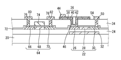
本実施形態の半導体装置92は、第一の実施形態の半導体装置10に比して、光センサ12の代わりに、光センサに関する本発明の第二の実施形態としての光センサ94を備えている。
この光センサ94は、第一の実施形態の光センサ12に比して、半導体層96が異なっている。半導体層96は、真性層40とp型層42がダイオード用半導体膜22のn型領域26上に順次積層されたものである。即ち、本実施形態における第二のフォトダイオード98は、n型領域26と真性層40とp型層42とを備えている。
半導体層96は、以下のようにして、形成することができる。先ず、後に真性層40となる真性半導体膜をプラズマCVDによって基板20の上側に形成する。これにより、層間絶縁膜34の上面及びコンタクトホール46,48,50,76,78内が、真性半導体膜で覆われる。
真性半導体膜は、真性半導体で形成されたアモルファスシリコン膜である。真性半導体膜をCVDによって形成する際の原料ガスとしては、例えば、シランガスと水素ガスを採用することができる。
真性半導体膜を形成したら、後にp型層42となるp型半導体膜をプラズマCVDによって真性半導体膜上に形成する。これにより、真性半導体膜の上面全体がp型半導体膜で覆われる。
p型半導体膜は、p型不純物がドーピングされたアモルファスシリコン膜である。p型半導体膜をCVDによって形成する際の原料ガスとしては、例えば、シランガスと水素ガスを採用することができる。p型半導体膜をCVDによって形成する際のドーピングガスとしては、例えば、ジボランを採用することができる。
このようにして、真性半導体膜とp型半導体膜を基板20の上側に順次形成した後、これらの半導体膜をフォトリソグラフィによってパターニングする。これにより、図6に示されているように、目的とする半導体層96が形成される。
このような半導体装置92においては、ダイオード用半導体膜22のn型領域26が第一のフォトダイオード16のn+領域と第二のフォトダイオード98のn+領域を兼ねている。従って、第一の実施形態の半導体装置10に比して、半導体層96を形成するのに必要な工程数を少なくすることができる。
[第三の実施形態]
続いて、半導体装置に関する本発明の第三の実施形態について、図7に基づいて、説明する。本実施形態の半導体装置100は、第一の実施形態の半導体装置10に比して、光センサ12の代わりに、光センサに関する本発明の第三の実施形態としての光センサ102を備えている。
続いて、半導体装置に関する本発明の第三の実施形態について、図7に基づいて、説明する。本実施形態の半導体装置100は、第一の実施形態の半導体装置10に比して、光センサ12の代わりに、光センサに関する本発明の第三の実施形態としての光センサ102を備えている。
この光センサ102は、第一の実施形態の光センサ12に比して、ダイオード用半導体膜103と、半導体層104と、半導体層104の形成位置とが異なっている。ダイオード用半導体膜103は、第一の実施形態で説明したダイオード用半導体膜22と比して、n型領域26とp型領域30の位置が逆になっている。半導体層104は、p型層42と真性層40とn型層38がダイオード用半導体膜22のp型領域30上に順次形成されたものである。即ち、本実施形態における第二のフォトダイオード106は、半導体層104を備えている。
半導体層104は、以下のようにして、形成することができる。先ず、後にp型層42となるp型半導体膜をプラズマCVDによって基板20の上側に形成する。これにより、層間絶縁膜34の上面及びコンタクトホール46,48,50,76,78内が、p型半導体膜で覆われる。
p型半導体膜は、p型不純物がドーピングされたアモルファスシリコン膜である。p型半導体膜をCVDによって形成する際の原料ガスとしては、例えば、シランガスと水素ガスを採用することができる。p型半導体膜をCVDによって形成する際のドーピングガスとしては、例えば、ジボランを採用することができる。
p型半導体膜を形成したら、後に真性層40となる真性半導体膜をプラズマCVDによってp型半導体膜上に形成する。これにより、p型半導体膜の上面全体が真性半導体膜で覆われる。
真性半導体膜は、真性半導体で形成されたアモルファスシリコン膜である。真性半導体膜をCVDによって形成する際の原料ガスとしては、例えば、シランガスと水素ガスを採用することができる。
真性半導体膜を形成したら、後にn型層38となるn型半導体膜をプラズマCVDによって真性半導体膜上に形成する。これにより、真性半導体膜の上面全体がn型半導体膜で覆われる。
n型半導体膜は、n型不純物がドーピングされたアモルファスシリコン膜である。n型半導体膜をCVDによって形成する際の原料ガスとしては、例えば、シランガスと水素ガスを採用することができる。n型半導体膜をCVDによって形成する際のドーピングガスとしては、例えば、ホスフィンを採用することができる。
このようにして、p型半導体膜と真性半導体膜とn型半導体膜を基板20の上側に順次形成した後、これらの半導体膜をフォトリソグラフィによってパターニングする。これにより、図7に示されているように、目的とする半導体層104が形成される。
[第四の実施形態]
続いて、半導体装置に関する本発明の第四の実施形態について、図8に基づいて、説明する。本実施形態の半導体装置108は、第一の実施形態の半導体装置10に比して、光センサ12の代わりに、光センサに関する本発明の第四の実施形態としての光センサ110を備えている。
続いて、半導体装置に関する本発明の第四の実施形態について、図8に基づいて、説明する。本実施形態の半導体装置108は、第一の実施形態の半導体装置10に比して、光センサ12の代わりに、光センサに関する本発明の第四の実施形態としての光センサ110を備えている。
この光センサ110は、第一の実施形態の光センサ12に比して、ダイオード用半導体膜111と、半導体層112と、半導体層112の形成位置とが異なっている。ダイオード用半導体膜111は、第一の実施形態で説明したダイオード用半導体膜22と比して、n型領域26とp型領域30の位置が逆になっている。半導体層112は、真性層40とn型層38がダイオード用半導体膜22のp型領域30上に順次形成されたものである。即ち、本実施形態における第二のフォトダイオード114は、p型領域30と真性層40とn型層38とを備えている。
半導体層112は、以下のようにして、形成することができる。先ず、後に真性層40となる真性半導体膜をプラズマCVDによって基板20の上側に形成する。これにより、層間絶縁膜34の上面及びコンタクトホール46,48,50,76,78内が、真性半導体膜で覆われる。
真性半導体膜は、真性半導体で形成されたアモルファスシリコン膜である。真性半導体膜をCVDによって形成する際の原料ガスとしては、例えば、シランガスと水素ガスを採用することができる。
真性半導体膜を形成したら、後にn型層38となるp型半導体膜をプラズマCVDによって真性半導体膜上に形成する。これにより、真性半導体膜の上面全体がn型半導体膜で覆われる。
n型半導体膜は、n型不純物がドーピングされたアモルファスシリコン膜である。n型半導体膜をCVDによって形成する際の原料ガスとしては、例えば、シランガスと水素ガスを採用することができる。n型半導体膜をCVDによって形成する際のドーピングガスとしては、例えば、ホスフィンを採用することができる。
このようにして、真性半導体膜とn型半導体膜を基板20の上側に順次形成した後、これらの半導体膜をフォトリソグラフィによってパターニングする。これにより、図6に示されているように、目的とする半導体層112が形成される。
このような半導体装置108においては、ダイオード用半導体膜22のp型領域30が第一のフォトダイオード16のp+領域と第二のフォトダイオード114のp+領域を兼ねている。これにより、第三の実施形態の半導体装置100に比して、半導体層112を形成するのに必要な工程数を少なくすることができる。
[第五の実施形態]
続いて、半導体装置に関する本発明の第五の実施形態について、図9に基づいて、説明する。本実施形態の半導体装置116は、第一の実施形態の半導体装置10に比して、電極・配線62と第二のフォトダイオード18の接続が異なっている。
続いて、半導体装置に関する本発明の第五の実施形態について、図9に基づいて、説明する。本実施形態の半導体装置116は、第一の実施形態の半導体装置10に比して、電極・配線62と第二のフォトダイオード18の接続が異なっている。
本実施形態の半導体装置116においては、半導体層36上に電極・配線44が形成されておらず、電極・配線62と半導体層36(p型層42)が直接に接続されている。これにより、半導体層36上に電極・配線44が形成されていることによる不具合、即ち、第二のフォトダイオード18の受光面積が小さくなる不具合を回避することができる。その結果、第二のフォトダイオード18の光検出感度を向上させることが可能となる。
[第六の実施形態]
続いて、半導体装置に関する本発明の第六の実施形態について、図10に基づいて、説明する。本実施形態の半導体装置118は、第一の実施形態の半導体装置10に比して、平坦化膜56上に電極・配線62が形成されていない。この場合、第一のフォトダイオード16のp+領域(p型領域30)と第二のフォトダイオード18のp+領域(p型層42)が電極・配線62を介さずに接続される。その結果、第一のフォトダイオード16のp+領域(p型領域30)と第二のフォトダイオード18のp+領域(p型層42)を低抵抗な電極・配線だけで接続することができる。
続いて、半導体装置に関する本発明の第六の実施形態について、図10に基づいて、説明する。本実施形態の半導体装置118は、第一の実施形態の半導体装置10に比して、平坦化膜56上に電極・配線62が形成されていない。この場合、第一のフォトダイオード16のp+領域(p型領域30)と第二のフォトダイオード18のp+領域(p型層42)が電極・配線62を介さずに接続される。その結果、第一のフォトダイオード16のp+領域(p型領域30)と第二のフォトダイオード18のp+領域(p型層42)を低抵抗な電極・配線だけで接続することができる。
以上、本発明の実施形態について、詳述してきたが、これらはあくまでも例示であって、本発明は、上述の実施形態によって、何等、限定されない。
例えば、第一~第六の実施形態において、ダイオード用半導体膜22を非晶質シリコンで形成し、半導体層36,96,104,112を結晶質シリコンで形成しても良い。この場合、トランジスタ用半導体膜64は、非晶質シリコンで形成されていても良いし、結晶質シリコンで形成されていても良い。ダイオード用半導体膜22を非晶質シリコンで形成し、トランジスタ用半導体膜64を結晶質シリコンで形成する方法としては、例えば、下地層24上に形成されたアモルファスシリコン膜において後にトランジスタ用半導体膜64となる領域に、非晶質シリコンの結晶化を促進する触媒元素をイオン注入等で導入した後、アモルファスシリコン膜をアニールする方法等を採用することができる。
第一~第六の実施形態において、ダイオード用半導体膜22における真性領域28を非晶質シリコンで形成し、半導体層36,96,104,112における真性層40を結晶質シリコンで形成しても良い。真性領域28を非晶質シリコンで形成する方法としては、例えば、下地層24上に形成されたアモルファスシリコン膜において後にn型領域26となる領域とp型領域30となる領域とに、非晶質シリコンの結晶化を促進する触媒元素をイオン注入等で導入した後、アモルファスシリコン膜をアニールする方法等を採用することが出来る。真性層40を結晶質シリコンで形成する方法としては、プラズマCVDやスパッタ等の従来から公知の方法を採用することができる。
第一~第六の実施形態において、半導体層36,96,104,112が備える層38,40,42のうち真性層40以外の層38,42をシリコンカーバイドやシリコンゲルマニウム、ゲルマニウム、化合物半導体、カルコゲナイド、ポリシリコン等で形成しても良い。
第一~第六の実施形態において、プラズマCVD等によって形成された半導体膜に不純物をイオンドーピングすることにより、n型層38とp型層42とを形成するようにしても良い。
前記第一~第六の実施形態において、半導体層36,96,104,112は、基板20の厚さ方向の投影において、真性領域28と重なる必要は必ずしもない。
Claims (12)
- 基板上に形成されて、n型領域と真性領域とp型領域を有するダイオード用半導体膜を備える第一のフォトダイオードと、
前記ダイオード用半導体膜上に形成されて、n型層とp型層の少なくとも一方と真性層を有する半導体層を含んで構成されると共に前記第一のフォトダイオードと並列に接続される第二のフォトダイオードと
を、備えており、
前記真性領域と前記真性層の一方が結晶質シリコンによって形成され、該真性領域と該真性層の他方が非晶質シリコンによって形成されている、光センサ。 - 前記ダイオード用半導体膜が前記結晶質シリコンによって形成されている、請求項1に記載の光センサ。
- 前記半導体層が、前記p型層と、前記真性層と、前記n型層を有している、請求項1又は2に記載の光センサ。
- 前記半導体層が、前記n型領域上に形成された前記真性層と、該真性層上に形成された前記p型層を有している、請求項1又は2に記載の光センサ。
- 前記半導体層が、前記p型領域上に形成された前記真性層と、該真性層上に形成された前記n型層を有している、請求項1又は2に記載の光センサ。
- 前記真性層の厚さが100nm~800nmとされている、請求項1~5の何れか1項に記載の光センサ。
- 前記ダイオード用半導体膜を覆うように形成された層間絶縁膜を更に備え、
前記層間絶縁膜上に前記半導体層が形成され、
前記層間絶縁膜を厚さ方向に貫通するように形成されたコンタクトホール内に前記半導体層が入り込んでおり、
前記コンタクトホール内において前記半導体層と前記ダイオード用半導体膜が接触している、請求項1~6の何れか1項に記載の光センサ。 - 前記半導体層が前記n型領域とp型領域の何れか一方だけに接触している、請求項7に記載の光センサ。
- 請求項1~8の何れか1項に記載の光センサと、
前記基板上に形成されて、チャネル領域、ソース領域及びドレイン領域を有するトランジスタ用半導体膜と、前記チャネル領域の導電性を制御するゲート電極と、該ゲート電極と前記トランジスタ用半導体膜の間に設けられたゲート絶縁膜とを有する薄膜トランジスタとを備えている、半導体装置。 - 前記ダイオード用半導体膜と前記トランジスタ用半導体膜が、それぞれ、前記結晶質シリコンによって形成されている、請求項9に記載の半導体装置。
- 前記基板上には、該基板からの不純物拡散を防ぐための下地層を更に備え、
前記ダイオード用半導体膜と前記トランジスタ用半導体膜が前記下地層上に形成されている、請求項9又は10に記載の半導体装置。 - 前記ダイオード用半導体膜の厚さと前記トランジスタ用半導体膜の厚さが同じである、請求項9~11の何れか1項に記載の半導体装置。
Applications Claiming Priority (2)
| Application Number | Priority Date | Filing Date | Title |
|---|---|---|---|
| JP2010164146 | 2010-07-21 | ||
| JP2010-164146 | 2010-07-21 |
Publications (1)
| Publication Number | Publication Date |
|---|---|
| WO2012011448A1 true WO2012011448A1 (ja) | 2012-01-26 |
Family
ID=45496870
Family Applications (1)
| Application Number | Title | Priority Date | Filing Date |
|---|---|---|---|
| PCT/JP2011/066261 Ceased WO2012011448A1 (ja) | 2010-07-21 | 2011-07-15 | 光センサ及び該光センサを備えた半導体装置 |
Country Status (1)
| Country | Link |
|---|---|
| WO (1) | WO2012011448A1 (ja) |
Cited By (1)
| Publication number | Priority date | Publication date | Assignee | Title |
|---|---|---|---|---|
| CN110970450A (zh) * | 2018-10-01 | 2020-04-07 | 力晶科技股份有限公司 | 影像传感器及其制造方法 |
Citations (7)
| Publication number | Priority date | Publication date | Assignee | Title |
|---|---|---|---|---|
| JPS6269568A (ja) * | 1985-09-20 | 1987-03-30 | Sharp Corp | 半導体カラ−センサ |
| JPS62203080A (ja) * | 1986-03-03 | 1987-09-07 | Toshiba Corp | 放射線検出装置 |
| JPH0315728A (ja) * | 1989-06-13 | 1991-01-24 | Mitsubishi Electric Corp | カラーフィルタ装置 |
| JP2006318947A (ja) * | 2005-05-10 | 2006-11-24 | Rohm Co Ltd | 受光装置およびそれを用いた電子機器 |
| JP2008135721A (ja) * | 2006-10-31 | 2008-06-12 | Semiconductor Energy Lab Co Ltd | 半導体装置 |
| JP2009010125A (ja) * | 2007-06-27 | 2009-01-15 | Sharp Corp | 半導体装置およびその製造方法 |
| WO2010095401A1 (ja) * | 2009-02-19 | 2010-08-26 | シャープ株式会社 | 半導体装置および表示装置 |
-
2011
- 2011-07-15 WO PCT/JP2011/066261 patent/WO2012011448A1/ja not_active Ceased
Patent Citations (7)
| Publication number | Priority date | Publication date | Assignee | Title |
|---|---|---|---|---|
| JPS6269568A (ja) * | 1985-09-20 | 1987-03-30 | Sharp Corp | 半導体カラ−センサ |
| JPS62203080A (ja) * | 1986-03-03 | 1987-09-07 | Toshiba Corp | 放射線検出装置 |
| JPH0315728A (ja) * | 1989-06-13 | 1991-01-24 | Mitsubishi Electric Corp | カラーフィルタ装置 |
| JP2006318947A (ja) * | 2005-05-10 | 2006-11-24 | Rohm Co Ltd | 受光装置およびそれを用いた電子機器 |
| JP2008135721A (ja) * | 2006-10-31 | 2008-06-12 | Semiconductor Energy Lab Co Ltd | 半導体装置 |
| JP2009010125A (ja) * | 2007-06-27 | 2009-01-15 | Sharp Corp | 半導体装置およびその製造方法 |
| WO2010095401A1 (ja) * | 2009-02-19 | 2010-08-26 | シャープ株式会社 | 半導体装置および表示装置 |
Cited By (1)
| Publication number | Priority date | Publication date | Assignee | Title |
|---|---|---|---|---|
| CN110970450A (zh) * | 2018-10-01 | 2020-04-07 | 力晶科技股份有限公司 | 影像传感器及其制造方法 |
Similar Documents
| Publication | Publication Date | Title |
|---|---|---|
| TWI478330B (zh) | 光電變換元件及其製造方法 | |
| JP4737956B2 (ja) | 表示装置および光電変換素子 | |
| US8097927B2 (en) | Highly sensitive photo-sensing element and photo-sensing device using the same | |
| CN102197485B (zh) | 半导体装置及其制造方法以及显示装置 | |
| JP6796150B2 (ja) | 撮像パネル及びその製造方法 | |
| US8829526B2 (en) | Semiconductor device, method for manufacturing same, and display device | |
| WO2011065057A1 (ja) | フォトダイオードおよびその製造方法、表示パネル用基板、表示装置 | |
| US8766337B2 (en) | Semiconductor device and method for manufacturing the same | |
| JP2008306080A (ja) | 光センサ素子、およびこれを用いた光センサ装置、画像表示装置 | |
| US20120242624A1 (en) | Thin film transistor and method for fabricating the same, semiconductor device and method for fabricating the same, as well as display | |
| WO2010035544A1 (ja) | フォトダイオードおよびその製造方法ならびにフォトダイオードを備えた表示装置 | |
| JP2008300630A (ja) | 半導体装置およびその製造方法 | |
| JP2004318067A (ja) | 画像表示装置およびその製造方法 | |
| TW201610459A (zh) | 攝像面板、攝像面板之製造方法、及x射線攝像裝置 | |
| US20110175535A1 (en) | Semiconductor device, method for manufacturing same and display device | |
| KR20000057997A (ko) | 이미지 센서의 구조 및 그 제조방법 | |
| WO2012011448A1 (ja) | 光センサ及び該光センサを備えた半導体装置 | |
| US8975637B2 (en) | Semiconductor device, process for production of the semiconductor device, and display device equipped with the semiconductor device | |
| CN111370524B (zh) | 感光传感器及其制备方法、阵列基板、显示面板 | |
| JP2006332287A (ja) | 薄膜ダイオード | |
| JP2009027035A (ja) | フォトダイオード、表示装置、及び表示装置の製造方法 | |
| US20130169914A1 (en) | Optical sensor and liquid crystal panel provided with the optical sensor | |
| US8466048B2 (en) | Selective recrystallization of semiconductor | |
| TW201230309A (en) | Photosensor and method of manufacturing the same | |
| JP5402211B2 (ja) | 光電変換装置の製造方法 |
Legal Events
| Date | Code | Title | Description |
|---|---|---|---|
| 121 | Ep: the epo has been informed by wipo that ep was designated in this application |
Ref document number: 11809618 Country of ref document: EP Kind code of ref document: A1 |
|
| NENP | Non-entry into the national phase |
Ref country code: DE |
|
| 122 | Ep: pct application non-entry in european phase |
Ref document number: 11809618 Country of ref document: EP Kind code of ref document: A1 |
|
| NENP | Non-entry into the national phase |
Ref country code: JP |