WO2012008198A1 - 光センサ付き表示装置 - Google Patents
光センサ付き表示装置 Download PDFInfo
- Publication number
- WO2012008198A1 WO2012008198A1 PCT/JP2011/060053 JP2011060053W WO2012008198A1 WO 2012008198 A1 WO2012008198 A1 WO 2012008198A1 JP 2011060053 W JP2011060053 W JP 2011060053W WO 2012008198 A1 WO2012008198 A1 WO 2012008198A1
- Authority
- WO
- WIPO (PCT)
- Prior art keywords
- voltage
- reset
- circuit
- sensor
- display device
- Prior art date
- Legal status (The legal status is an assumption and is not a legal conclusion. Google has not performed a legal analysis and makes no representation as to the accuracy of the status listed.)
- Ceased
Links
Images








Classifications
-
- H—ELECTRICITY
- H10—SEMICONDUCTOR DEVICES; ELECTRIC SOLID-STATE DEVICES NOT OTHERWISE PROVIDED FOR
- H10F—INORGANIC SEMICONDUCTOR DEVICES SENSITIVE TO INFRARED RADIATION, LIGHT, ELECTROMAGNETIC RADIATION OF SHORTER WAVELENGTH OR CORPUSCULAR RADIATION
- H10F39/00—Integrated devices, or assemblies of multiple devices, comprising at least one element covered by group H10F30/00, e.g. radiation detectors comprising photodiode arrays
- H10F39/80—Constructional details of image sensors
-
- G—PHYSICS
- G06—COMPUTING OR CALCULATING; COUNTING
- G06F—ELECTRIC DIGITAL DATA PROCESSING
- G06F3/00—Input arrangements for transferring data to be processed into a form capable of being handled by the computer; Output arrangements for transferring data from processing unit to output unit, e.g. interface arrangements
- G06F3/01—Input arrangements or combined input and output arrangements for interaction between user and computer
- G06F3/03—Arrangements for converting the position or the displacement of a member into a coded form
- G06F3/041—Digitisers, e.g. for touch screens or touch pads, characterised by the transducing means
- G06F3/0412—Digitisers structurally integrated in a display
-
- G—PHYSICS
- G06—COMPUTING OR CALCULATING; COUNTING
- G06F—ELECTRIC DIGITAL DATA PROCESSING
- G06F3/00—Input arrangements for transferring data to be processed into a form capable of being handled by the computer; Output arrangements for transferring data from processing unit to output unit, e.g. interface arrangements
- G06F3/01—Input arrangements or combined input and output arrangements for interaction between user and computer
- G06F3/03—Arrangements for converting the position or the displacement of a member into a coded form
- G06F3/041—Digitisers, e.g. for touch screens or touch pads, characterised by the transducing means
- G06F3/042—Digitisers, e.g. for touch screens or touch pads, characterised by the transducing means by opto-electronic means
-
- G—PHYSICS
- G09—EDUCATION; CRYPTOGRAPHY; DISPLAY; ADVERTISING; SEALS
- G09G—ARRANGEMENTS OR CIRCUITS FOR CONTROL OF INDICATING DEVICES USING STATIC MEANS TO PRESENT VARIABLE INFORMATION
- G09G3/00—Control arrangements or circuits, of interest only in connection with visual indicators other than cathode-ray tubes
- G09G3/20—Control arrangements or circuits, of interest only in connection with visual indicators other than cathode-ray tubes for presentation of an assembly of a number of characters, e.g. a page, by composing the assembly by combination of individual elements arranged in a matrix no fixed position being assigned to or needed to be assigned to the individual characters or partial characters
- G09G3/34—Control arrangements or circuits, of interest only in connection with visual indicators other than cathode-ray tubes for presentation of an assembly of a number of characters, e.g. a page, by composing the assembly by combination of individual elements arranged in a matrix no fixed position being assigned to or needed to be assigned to the individual characters or partial characters by control of light from an independent source
- G09G3/3406—Control of illumination source
-
- G—PHYSICS
- G09—EDUCATION; CRYPTOGRAPHY; DISPLAY; ADVERTISING; SEALS
- G09G—ARRANGEMENTS OR CIRCUITS FOR CONTROL OF INDICATING DEVICES USING STATIC MEANS TO PRESENT VARIABLE INFORMATION
- G09G3/00—Control arrangements or circuits, of interest only in connection with visual indicators other than cathode-ray tubes
- G09G3/20—Control arrangements or circuits, of interest only in connection with visual indicators other than cathode-ray tubes for presentation of an assembly of a number of characters, e.g. a page, by composing the assembly by combination of individual elements arranged in a matrix no fixed position being assigned to or needed to be assigned to the individual characters or partial characters
- G09G3/34—Control arrangements or circuits, of interest only in connection with visual indicators other than cathode-ray tubes for presentation of an assembly of a number of characters, e.g. a page, by composing the assembly by combination of individual elements arranged in a matrix no fixed position being assigned to or needed to be assigned to the individual characters or partial characters by control of light from an independent source
- G09G3/36—Control arrangements or circuits, of interest only in connection with visual indicators other than cathode-ray tubes for presentation of an assembly of a number of characters, e.g. a page, by composing the assembly by combination of individual elements arranged in a matrix no fixed position being assigned to or needed to be assigned to the individual characters or partial characters by control of light from an independent source using liquid crystals
- G09G3/3611—Control of matrices with row and column drivers
- G09G3/3648—Control of matrices with row and column drivers using an active matrix
Definitions
- the present invention relates to a display device, and more particularly to a display device in which a plurality of photosensors are arranged in a pixel region.
- a method of providing a plurality of optical sensors on a display panel and providing an input function such as a touch panel, a pen input, and a scanner is known for display devices.
- an input function such as a touch panel, a pen input, and a scanner.
- a method is also known in which a component that is affected by the light environment is removed from a signal detected by an optical sensor and a signal to be originally input is obtained.
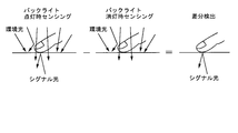
- a backlight difference method shown in FIG. 16 is known.
- the optical sensor Detect both light and ambient light. Therefore, in the backlight difference method, sensing is performed both in a state where the backlight is turned on and in a state where the backlight is turned off. Signal light and ambient light are detected when sensing when the backlight is turned on, and ambient light is detected when sensing when the backlight is turned off. Therefore, only the signal light can be extracted by obtaining the difference between the two sensing results.
- an input function independent of the light environment can be provided.
- a transistor hereinafter referred to as a charge holding transistor
- the charge holding transistor is on / off controlled.
- timing for resetting and reading out the sensor circuit and timing for controlling on / off of the charge holding transistor.
- Patent Document 1 includes a photoelectric conversion element, a capacitive element, and a sensor unit including a switching element provided between the reset line and the capacitive element, and a reset signal is asserted. Describes a liquid crystal device that reads a reference light reception signal and reads a measurement light reception signal after a predetermined time has elapsed after negating a reset signal.
- the charge holding transistor is provided in series with the photosensor between the reset terminal and the storage node (see FIG. 3 described later).
- the charge holding transistor is controlled to be in an on state during a sensing period, and is controlled to be in an off state during a holding period for holding a sensing result.
- a leak current flows through the charge holding transistor, so that the amount of charge accumulated in the accumulation node changes. For this reason, in a display device including a sensor circuit including a charge holding transistor, there is a problem that noise is mixed in the output of the sensor circuit and the light detection accuracy is lowered.
- an object of the present invention is to provide a display device that suppresses leakage current flowing through a charge holding transistor and has high photodetection accuracy.
- a first aspect of the present invention is a display device in which a plurality of photosensors are arranged in a pixel region, A display panel including a plurality of pixel circuits and a plurality of sensor circuits; A drive circuit for driving the pixel circuit and the sensor circuit; The sensor circuit is An accumulation node for accumulating charges according to the detected light amount; An optical sensor provided between the storage node and a reset line controlled by the drive circuit; A charge holding transistor provided in series with the photosensor and controlled to be turned on / off by the driving circuit, The drive circuit applies a holding voltage for reducing a voltage between conduction terminals of the charge holding transistor to the reset line while controlling the charge holding transistor in an off state.
- the drive circuit applies a reset voltage as the holding voltage to the reset line.
- the drive circuit applies a voltage between a reset voltage and a reset release voltage as the holding voltage to the reset line.
- the drive circuit applies a voltage approximately in the middle of the reset voltage and the voltage of the storage node at the time of detecting the maximum light amount as the holding voltage to the reset line.
- a light source that is turned on and off at a predetermined cycle;
- the sensor circuit includes a first sensor circuit and a second sensor circuit;
- the drive circuit controls the charge holding transistor in the first sensor circuit to be on while the light source is turned off, and the charge holding transistor in the second sensor circuit while the light source is turned on. Is controlled to be in an on state.
- a sixth aspect of the present invention is the fifth aspect of the present invention,
- the drive circuit performs line-sequential readout from the first and second sensor circuits while controlling all the charge retention transistors in the first and second sensor circuits to be in an OFF state.
- a seventh aspect of the present invention is the sixth aspect of the present invention,
- the driving circuit is characterized in that reading from the first sensor circuit and reading from the second sensor circuit are performed in parallel.
- One end of the photosensor is connected to the reset line, the other end is connected to one conduction terminal of the charge holding transistor, and the other conduction terminal of the charge holding transistor is connected to the storage node.
- a ninth aspect of the present invention is the eighth aspect of the present invention,
- the sensor circuit further includes a read transistor having a control terminal connected to the storage node.
- the sensor circuit further includes a capacitor provided between the storage node and a readout line controlled by the driving circuit.
- the voltage between the conduction terminals of the charge holding transistor can be reduced and the leakage current flowing through the charge holding transistor can be suppressed. it can. Therefore, a change in the voltage of the storage node during the holding period can be suppressed, and the light detection accuracy can be increased.
- the voltage between the conduction terminals of the charge holding transistor is reduced without generating a new voltage, and the leakage current flowing through the charge holding transistor Can be suppressed. Therefore, the light detection accuracy can be increased with a simple circuit.
- the third aspect of the present invention by using a suitable voltage between the reset voltage and the reset release voltage as the holding voltage, the voltage between the conduction terminals of the charge holding transistor is further reduced, and the charge holding transistor The leakage current flowing through can be further suppressed. Therefore, the light detection accuracy can be further increased by using a suitable voltage.
- the voltage between the conduction terminals of the charge holding transistor can be further reduced by using a voltage approximately in the middle of the reset voltage and the voltage of the storage node at the time of detecting the maximum light amount as the holding voltage. Leakage current flowing through the charge holding transistor can be further suppressed. Therefore, the light detection accuracy can be further increased by using a suitable voltage.
- the amount of light when the light source is turned off and the amount of light when the light source is turned on can be separately detected using two types of sensor circuits, and the difference between the two can be obtained outside the sensor circuit. Therefore, the light emitted from the light source can be used as signal light to provide an input function independent of the light environment.
- the degree of freedom in determining sensing and readout timing can be increased by performing sensing by the sensor circuit and readout from the sensor circuit in different periods.
- reading from the first sensor circuit and reading from the second sensor circuit are performed in parallel, thereby reducing the reading speed and reducing the power consumption of the display device. Can do.
- the light sensor and the charge retention transistor are connected in series, one end thereof is connected to the reset line, and the other end is connected to the storage node, so that the light incident in a predetermined period It is possible to configure a sensor circuit that detects only the above.
- a read transistor is provided in the sensor circuit, and a predetermined voltage is applied to one conduction terminal of the read transistor, so that the voltage from the other conduction terminal of the read transistor to the voltage of the storage node is determined.
- the signal corresponding to the detected light amount can be read out from the sensor circuit.
- the tenth aspect of the present invention by providing a capacitor in the sensor circuit and applying a read voltage to the read line, the voltage of the storage node is changed, and a signal corresponding to the detected light amount is read from the sensor circuit. Can do.
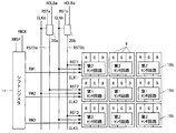
- FIG. 2 is a diagram illustrating an arrangement of sensor circuits and a configuration of a sensor row driver circuit in the display device illustrated in FIG. 1.
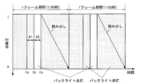
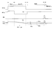
- FIG. 2 is a circuit diagram of a sensor circuit included in the display circuit shown in FIG. 1. It is a figure which shows the lighting and extinguishing timing of the backlight in the display apparatus shown in FIG. 1, and the reset and reading timing with respect to a sensor circuit.
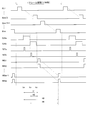
- FIG. 2 is a signal waveform diagram of a display panel in the display device shown in FIG. 1.
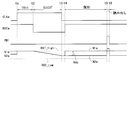
- FIG. 2 is a signal waveform diagram of a first sensor circuit in the display device shown in FIG. 1.
- FIG. 11 is a circuit diagram of a reset control circuit included in the sensor row driver circuit shown in FIG. 10. It is a signal waveform diagram of the display panel in the display device according to the second embodiment of the present invention. It is a signal waveform diagram of the 1st sensor circuit in the display concerning a 2nd embodiment of the present invention.
- FIG. 1 is a block diagram showing a configuration of a display device according to the first embodiment of the present invention.
- the display device shown in FIG. 1 includes a display control circuit 1, a display panel 2, and a backlight 3.
- the display panel 2 includes a pixel region 4, a gate driver circuit 5, a source driver circuit 6, a sensor row driver circuit 7, and a sensor column driver circuit 8.
- the pixel region 4 includes a plurality of pixel circuits 9 and a plurality of sensor circuits 10.
- This display device has a function of displaying an image on the display panel 2 and a function of detecting light incident on the display panel 2.
- m and n are even numbers, i is an even number of m or less, and j is an even number of 2n or less, and the frame rate of the display device is 60 frames / second.
- the video signal Vin and the timing control signal Cin are supplied from the outside to the display device shown in FIG. Based on these signals, the display control circuit 1 outputs a video signal VS and control signals CSg, CSs, and CSr to the display panel 2 and outputs a control signal CSb to the backlight 3.
- the video signal VS may be the same as the video signal Vin, or may be a signal obtained by performing signal processing on the video signal Vin.
- the backlight 3 is a light source that irradiates the display panel 2 with light. More specifically, the backlight 3 is provided on the back side of the display panel 2 and irradiates the back surface of the display panel 2 with light. The backlight 3 is turned on when the control signal CSb is at a high level, and is turned off when the control signal CSb is at a low level.
- the backlight 3 is configured using, for example, an infrared LED (Light Emitting Diode) that emits infrared light.
- (m ⁇ 3n) pixel circuits 9 and (m ⁇ n) sensor circuits 10 are two-dimensionally arranged. More specifically, the pixel region 4 is provided with m gate lines GL1 to GLm and 3n source lines SL1 to SL3n. Gate lines GL1 to GLm are arranged in parallel to each other, and source lines SL1 to SL3n are arranged in parallel to each other so as to be orthogonal to gate lines GL1 to GLm.
- the (m ⁇ 3n) pixel circuits 9 are arranged in the vicinity of the intersections of the gate lines GL1 to GLm and the source lines SL1 to SL3n.
- Each pixel circuit 9 is connected to one gate line GL and one source line SL.
- the pixel circuit 9 is classified into red display, green display, and blue display. These three types of pixel circuits 9 are arranged side by side in the extending direction of the gate lines GL1 to GLm, and constitute one color pixel.
- m control lines CLK1 to CLKm, m reset lines RST1 to RSTm, and m readout lines RW1 to RWm are provided in parallel with the gate lines GL1 to GLm.
- 2n output lines OUT1 to OUT2n are provided in parallel with the source lines SL1 to SL3n.
- the pixel region 4 is provided with a power supply line VDD to which a predetermined power supply voltage is fixedly applied.
- the (m ⁇ n) sensor circuits 10 are provided in the vicinity of the intersections of the odd-numbered read lines RW1, RW3,... And the odd-numbered output lines OUT1, OUT3, etc., and the even-numbered read lines RW2, RW4,. And the even-numbered output lines OUT2, OUT4,...
- Each sensor circuit 10 is connected to one control line CLK, one reset line RST, one readout line RW, one output line OUT, and a power supply line VDD.
- the gate driver circuit 5, the source driver circuit 6, the sensor row driver circuit 7, and the sensor column driver circuit 8 function as drive circuits that drive the pixel circuit 9 and the sensor circuit 10.
- the gate driver circuit 5 is arranged along one side (right side in FIG. 1) of the pixel region 4.
- the sensor row driver circuit 7 is arranged along the opposite side (left side in FIG. 1) of the pixel region 4.
- the source driver circuit 6 and the sensor column driver circuit 8 are arranged along the other side (upper side in FIG. 1) of the display area.
- These driving circuits may be formed monolithically on the display panel 2 together with the pixel circuit 9 and the sensor circuit 10 or may be built in an IC chip mounted on the display panel 2.
- the gate driver circuit 5 drives the gate lines GL1 to GLm based on the control signal CSg. More specifically, the gate driver circuit 5 sequentially selects one gate line from the gate lines GL1 to GLm based on the control signal CSg, applies a high level voltage to the selected gate line, and applies to the remaining gate lines. Apply low level voltage. Thereby, the 3n pixel circuits 9 connected to the selected gate line are selected at once.
- the source driver circuit 6 drives the source lines SL1 to SL3n based on the control signal CSs. More specifically, the source driver circuit 6 applies a voltage corresponding to the video signal VS to the source lines SL1 to SL3n based on the control signal CSs. At this time, the source driver circuit 6 may perform line sequential driving or dot sequential driving. The voltages applied to the source lines SL1 to SL3n are written into 3n pixel circuits 9 selected by the gate driver circuit 5. In this way, a desired image can be displayed on the display panel 2 by writing a voltage corresponding to the video signal VS to all the pixel circuits 9 using the gate driver circuit 5 and the source driver circuit 6.
- the sensor row driver circuit 7 drives the control lines CLK1 to CLKm, the reset lines RST1 to RSTm, and the readout lines RW1 to RWm based on the control signal CSr (details will be described later).
- the sensor row driver circuit 7 applies a high level voltage to the even-numbered control lines while applying a low level voltage to the even-numbered reset lines in the first sensing period based on the control signal CSr.
- the sensor row driver circuit 7 applies a high level voltage to the odd-numbered control lines while applying a low-level voltage to the odd-numbered reset lines in the second sensing period.
- the sensor circuit 10 detects incident light when a low level voltage is applied to the reset line RST and a high level voltage is applied to the control line CLK.
- the sensor row driver circuit 7 sequentially selects two adjacent read lines from the read lines RW1 to RWm based on the control signal CSr, and applies a high level voltage to the selected read line. As a result, 2n signals are output to the output lines OUT1 to OUT2n from the 2n sensor circuits 10 connected to the selected readout line.
- the sensor column driver circuit 8 includes a difference circuit (not shown) for obtaining a difference between an output signal of the odd-numbered sensor circuit 10 and an output signal of the even-numbered sensor circuit 10.
- the sensor column driver circuit 8 amplifies the signal difference obtained by the difference circuit, and outputs the amplified signal to the outside of the display panel 2 as the sensor output Sout.
- FIG. 2 is a diagram showing the arrangement of the sensor circuit 10 and the configuration of the sensor row driver circuit 7.
- (m ⁇ n) sensor circuits 10 include a first sensor circuit 10 a that detects light that is incident during the extinguishing period of the backlight 3, and light that is incident during the lighting period of the backlight 3.
- the second sensor circuit 10b to be detected is classified.
- the first sensor circuit 10a and the second sensor circuit 10b are the same number.
- (M ⁇ n / 2) first sensor circuits 10a are arranged in even rows
- (m ⁇ n / 2) second sensor circuits 10b are arranged in odd rows.
- the odd-numbered control lines CLK1, CLK3,... Are all connected to the control line CLKb.
- the even-numbered control lines CLK2, CLK4,... Are all connected to the control line CLKa.
- the odd-numbered reset lines RST1, RST3,... Are all connected to the reset line RSTb.
- the even-numbered reset lines RST2, RST4,... are all connected to the reset line RSTa.
- the first sensor circuit 10a is connected to the control line CLKa via the even-numbered control line, and is connected to the reset line RSTa via the even-numbered reset line.
- the second sensor circuit 10b is connected to the control line CLKb via an odd-numbered control line, and is connected to the reset line RSTb via an odd-numbered reset line.
- the sensor row driver circuit 7 includes an m-stage shift register 11.
- the shift register 11 sequentially shifts the pulse signal RWSP input to the first stage based on the clock signal RWCK. Signals output from each stage of the shift register 11 sequentially become high level.
- the m signals output from the shift register 11 are applied to the read lines RW1 to RWm, respectively.
- FIG. 3 is a circuit diagram of the sensor circuit 10.
- the first sensor circuit 10a includes TFTs (ThinThFilm Transistors): Ta, Ma, a photodiode Da, and a capacitor Ca.
- the second sensor circuit 10b includes TFTs: Tb and Mb, a photodiode Db, and a capacitor Cb.
- TFT: Ta, Ma, Tb, and Mb are all N-channel TFTs.
- the photodiodes Da and Db function as photosensors
- the TFTs: Ta and Tb function as charge holding transistors
- the TFTs: Ma and Mb function as read transistors.
- the anode of the photodiode Da is connected to the reset terminal, and the cathode is connected to the source of TFT: Ta.
- the gate of TFT: Ta is connected to the control terminal, and the drain is connected to the gate of TFT: Ma.
- the drain of the TFT: Ma is connected to the power supply terminal, and the source is connected to the output terminal.
- the capacitor Ca is provided between the gate of the TFT: Ma and the readout terminal.
- a node where the photodiode Da and the TFT: Ta are connected is referred to as a node N1a
- a node where the TFT: Ta, Ma and the capacitor Ca are connected is referred to as a node N2a.
- the node N2a functions as an accumulation node that accumulates charges according to the detected light amount.
- the control terminal of the first sensor circuit 10a is connected to the control line CLKa via an even-numbered control line.
- the reset terminal is connected to the reset line RSTa via an even-numbered reset line.
- the read terminal is connected to the even-numbered read line RWi.
- the output terminal is connected to the even-numbered output line OUTj.
- the power supply terminal is connected to the power supply line VDD.
- the second sensor circuit 10b has the same configuration as the first sensor circuit 10a. However, the control terminal of the second sensor circuit 10b is connected to the control line CLKb via an odd-numbered control line.
- the reset terminal is connected to the reset line RSTb via an odd-numbered reset line.
- the read terminal is connected to the odd-numbered read line RWi-1.
- the output terminal is connected to the odd-numbered output line OUTj-1.
- FIG. 4 is a diagram showing lighting and extinguishing timings of the backlight 3, and resetting and reading timings for the sensor circuit 10.
- the backlight 3 is turned on once every frame period for a predetermined time, and is turned off in other periods. Specifically, the backlight 3 is turned on at time tb within one frame period and turned off at time tc. In this way, the backlight 3 is turned on and off at a predetermined cycle.
- the first sensor circuit 10a detects light incident in the first sensing period A1 (sensing period when the backlight 3 is turned off) from time ta to time tb.
- the second sensor circuit 10b detects light incident during the second sensing period A2 (sensing period when the backlight 3 is turned on) from time tb to time tc.
- the lengths of the first sensing period A1 and the second sensing period A2 are the same.
- the reset for the first sensor circuit 10a is continuously performed outside the first sensing period A1, and the reset for the second sensor circuit 10b is continuously performed outside the second sensing period A2. Reading from the first sensor circuit 10a and reading from the second sensor circuit 10b are performed line-sequentially in parallel after time tc.
- FIG. 5 is a signal waveform diagram of the display panel 2.
- the same name as the signal line is used (for example, the signal on the control line CLKa is referred to as a control signal CLKa).
- the gate signals GL1 to GLm are set to the high level for a predetermined time in order once every frame period.
- the control signal CLKa is at a high level once in one frame period in the first sensing period A1 (more specifically, from time ta to a little before time tb), and at a low level otherwise.
- the control signal CLKb becomes a high level once in one frame period in the second sensing period A2 (more specifically, from time tb to slightly before time tc), and otherwise becomes a low level.
- the reset signal RSTa becomes a low level in the first sensing period A1 (more specifically, from a little after the time ta to a little before the time tb), and otherwise becomes a high level.
- the reset signal RSTb becomes a low level in the second sensing period A2 (more specifically, from a little later than the time tb to a little before the time tc), and otherwise becomes a high level.
- the read signals RW1 to RWm are paired in pairs, and (m / 2) pairs of read signals sequentially go high for a predetermined time after time tc.
- FIG. 6 is a signal waveform diagram of the first sensor circuit 10a.
- FIG. 6 shows changes in the voltages of the nodes N1a and N2a.
- the reset period is from time ta to time t2
- the sensing period is from time t2 to time t3
- the holding period is from time t4 to time t5
- the readout period is from time t5 to time t6.
- the control signal CLKa is at a high level during the reset period and the sensing period, and is at a low level otherwise.
- the reset signal RSTa is at a low level during the sensing period and the period from time t3 to time t4, and is at a high level otherwise.
- the read signal RWi is at a high level during the read period, and is at a low level otherwise.
- the control signal CLKa and the reset signal RSTa are at a high level, and the read signal RWi is at a low level.
- TFT: Ta is in an on state. Accordingly, a current (forward current of the photodiode Da) flows from the reset line RSTa to the node N2a via the photodiode Da and the TFT: Ta, and the voltage of the node N2a is reset to a high level.
- the control signal CLKa remains high, the read signal RWi remains low, and the reset signal RSTa becomes low.
- TFT: Ta is still on.
- the voltage of the node N2a falls according to the amount of light incident during the sensing period (the sensing period when the backlight 3 is turned off). Note that in the reset period and the sensing period, since the TFT: Ta is on, the voltage at the node N1a is equal to the voltage at the node N2a.
- the control signal CLKa becomes low level.
- the TFT: Ta is turned off, and the nodes N1a and N2a are electrically disconnected.
- the control signal CLKa and the read signal RWi remain at low level, and the reset signal RSTa becomes high level.
- the TFT: Ta is in an off state, and the nodes N1a and N2a are electrically disconnected. For this reason, even if light enters the photodiode Da, the voltage at the node N2a does not change. On the other hand, the voltage of the node N1a is reset to a high level (see the thick broken line in FIG. 6).
- the drain-source voltage Vds of TFT: Ta is the difference between the voltage at the node N1a and the voltage at the node N2a.
- the control signal CLKa remains at low level
- the reset signal RSTa remains at high level
- the read signal RWi becomes high level.
- TFT: Ta is continuously off.
- the voltage at the node N2a increases by a predetermined multiple of the amount of increase in the voltage of the read signal RWi (the multiplier is determined by the ratio between the capacitance value of the capacitor Ca and the overall capacitance value of the first sensor circuit 10a).
- the TFT: Ma constitutes a source follower amplifier circuit using a transistor (not shown) included in the sensor column driver circuit 8 as a load, and drives the output line OUTa according to the voltage of the node N2a.
- the first sensor circuit 10a outputs a signal corresponding to the amount of light incident during the first sensing period A1 (the sensing period when the backlight 3 is turned off).
- the second sensor circuit 10b operates in the same manner as the first sensor circuit 10a, and outputs a signal corresponding to the amount of light incident during the second sensing period A2 (the sensing period when the backlight 3 is lit). Therefore, by using the difference circuit included in the sensor column driver circuit 8, the difference between the output signal of the first sensor circuit 10a and the output signal of the second sensor circuit 10b is obtained, so that the amount of light when the backlight is turned on and the backlight is turned off. The difference in the amount of light at the time can be obtained.
- the display device has a holding voltage for reducing the drain-source voltage Vds of the TFTs: Ta, Tb while the TFTs: Ta, Tb are controlled to be in an off state (that is, outside the sensing period). Apply to the reset lines RSTa and RSTb.
- the display device applies a high level voltage (reset voltage) to the reset line RST as a holding voltage except during the sensing period.
- reset voltage high level voltage
- the effects of the display device according to the present embodiment will be described in comparison with a display device that applies a low level voltage (reset release voltage) to the reset line RST outside the sensing period (hereinafter referred to as a display device according to a reference example). To do.
- the reset signal RSTa becomes a high level during a part of the first sensing period (more specifically, for a predetermined time from a little later than the time ta). Otherwise, it is low level.
- the reset signal RSTb is at a high level during a part of the second sensing period A2 (more specifically, for a predetermined time after a short time after the time tb), and at a low level otherwise. As shown in FIG. 8, the reset signal RSTa becomes high level only in the reset period (time t1 to t2).
- FIG. 9 is a diagram showing the IV characteristics of the photodiode.
- FIG. 9 shows IV characteristics when the amount of incident light is switched to three levels of X1 to X3 (where X1 ⁇ X2 ⁇ X3).
- the horizontal axis represents the bias voltage Vac applied to the photodiode
- the vertical axis represents the absolute value of the current I flowing through the photodiode.
- a negative bias voltage Vac is applied, a reverse current flows through the photodiode.
- the bias voltage Vac is within the range R (range V2 to V1) shown in FIG. 9, the reverse current is substantially constant.
- the photodiode is preferably used under the condition that the current does not change even when the bias voltage Vac changes, and the current changes linearly when the amount of incident light changes. Therefore, when the photodiode having the IV characteristic shown in FIG. 9 is used, the bias voltage Vac within the range R is applied. Note that the values of the voltages V1 and V2 vary depending on the manufacturing process and the device structure.
- of the bias voltage immediately after the reset becomes
- the low level voltage of the reset signal RSTa is determined.
- the voltage at the node N2a gradually decreases, and the absolute value
- of the bias voltage at the end of the sensing period is greater than or equal to
- the low level voltage of the reset signal is ⁇ 5 V
- the high level voltage of the reset signal is 0 V
- a bias voltage Vac of ⁇ 5 V to ⁇ 2 V is applied to the photodiode.
- the voltage of the node N1a changes in the range of ⁇ 5V to 0V
- the voltage of the node N2a changes in the range of ⁇ 3V to 0V.
- the leakage current flowing through the TFT: Ta is maximized because the voltage at the node N1a is ⁇ 5V. This is when the voltage of the node N2a is 0V.
- of the drain-source voltage of TFT: Ta is 5V. Therefore, a leak current corresponding to
- 5V flows through the TFTs: Ta and Tb. For this reason, in the display device according to the reference example, noise due to a leakage current corresponding to 5 V is mixed in the output of the sensor circuit, and the light detection accuracy is lowered accordingly.
- sensing by the first sensor circuit 10a and sensing by the second sensor circuit 10b are performed in different periods.
- the length of the holding period is different between the sensor circuit 10 that performs reading first and the sensor circuit 10 that performs reading last.
- the holding period of the first sensor circuit 10a to be read first is H1
- the holding period of the second sensor circuit 10b to be read first is H2
- the first sensor circuit 10a to be read last is held.
- the leakage current flowing through the TFTs: Ta and Tb causes variations in the output of the sensor circuit due to the difference in the length of the holding period, and light detection. Accuracy is reduced.
- a high-level voltage is applied to the reset line RST as a holding voltage while the TFT: Ta is controlled to be turned off, thereby suppressing a leakage current flowing through the TFT: Ta.
- the light detection accuracy can be increased.
- the conduction terminal of the charge holding transistor (TFT: Ta, Tb)
- a holding voltage for reducing the voltage between the reset lines RSTa and RSTb is applied.
- the voltage between the conduction terminals of the charge holding transistor can be reduced, and the leakage current flowing through the charge holding transistor can be suppressed. Therefore, charges corresponding to the detected light amount can be accumulated in the accumulation node with high accuracy, and the detection accuracy of the photosensor can be increased.
- the reset voltage high level voltage
- the voltage between the conduction terminals of the charge holding transistor is reduced without generating a new voltage, and the leakage current flowing through the charge holding transistor is suppressed. Can do. Therefore, the detection accuracy of the optical sensor can be increased with a simple circuit.
- the light quantity when the light source (backlight 3) is turned off and the light quantity when the light source is turned on are separately detected using two types of sensor circuits 10a and 10b, and the difference between the two is obtained outside the sensor circuits 10a and 10b. it can. Accordingly, it is possible to provide an input function that does not depend on the light environment by using the light emitted from the light source as the signal light.
- sensing and reading for the two types of sensor circuits 10a and 10b in different periods it is possible to increase the degree of freedom when determining sensing and reading timing. Further, by performing reading from the first sensor circuit 10a and reading from the second sensor circuit 10b in parallel, the reading speed can be reduced and the power consumption of the display device can be reduced.
- a photosensor photodiode Da
- a charge holding transistor TFT: Ta
- a reset line RSTa reset line
- a storage node node N2a
- VDD power supply voltage
- a capacitor (capacitor Ca) is provided in the sensor circuit, and by applying a read voltage (high level voltage) to the read line RWi, the voltage of the storage node is changed, and a signal corresponding to the detected light amount is read from the sensor circuit. be able to.
- the display device according to the second embodiment of the present invention has the same configuration as the display device according to the first embodiment, and includes the same pixel circuit (see FIGS. 1 and 3). This embodiment is different from the first embodiment in the level of the holding voltage applied to the reset line. Hereinafter, differences from the first embodiment will be described.
- FIG. 10 is a diagram showing the arrangement of the sensor circuit 10 and the configuration of the sensor row driver circuit 7 in the display device according to the present embodiment.
- the odd-numbered reset lines RST1, RST3,... Are all connected to the reset line RSTOb.
- the even-numbered reset lines RST2, RST4,... Are all connected to the reset line RSTOa.
- the sensor row driver circuit 7 includes a reset control circuit 20a that outputs a reset signal RSTOa and a reset control circuit 20b that outputs a reset line RSTOb.
- FIG. 11 is a circuit diagram of the reset control circuit 20a.
- the reset control circuit 20a includes four analog switches 21-24. Control signals CLKa, HOLBa, a reset signal RSTa, a high level voltage RST_High, a low level voltage RST_Low, and an intermediate voltage Vm are input to the reset control circuit 20a.
- the reset signal RSTa is at a low level
- the analog switch 23 is turned on, the analog switch 24 is turned off, and the voltage of the reset signal RSTa becomes equal to the low level voltage RST_Low.
- the analog switches 21 and 24 are in an on state, the analog switches 22 and 23 are in an off state, and the voltage of the reset signal RSTOa is at a high level. It becomes equal to the voltage RST_High.
- the reset signal RSTa is at a high level and both the control signals CLKa and HOLBa are at a low level, the analog switches 22 and 24 are turned on, the analog switches 21 and 23 are turned off, and the voltage of the reset signal RSTOa is set to the intermediate voltage Vm. Will be equal.
- the reset control circuit 20b has the same configuration as the reset control circuit 20a.
- the reset signal RSTa becomes high level at the beginning of the first sensing period (more specifically, only for a predetermined time from the time ta), and the first sensing It becomes a low level in the remainder of the period (more specifically, after a predetermined time elapses from time ta until slightly before time tb), and otherwise becomes an intermediate level (intermediate voltage Vm).
- the reset signal RSTb becomes a high level at the beginning of the second sensing period (more specifically, for a predetermined time from the time tb), and the predetermined time has elapsed from the remaining part of the second sensing period (more specifically, from the time tb). After that, it goes low until a little before time tc), otherwise it is at an intermediate level.
- the reset signal RSTa is at a high level during the reset period (time ta to t2), and is at a low level during the sensing period (time t2 to t3) and the period from time t3 to time t4. Become an intermediate level.
- the intermediate voltage Vm is a voltage between the reset voltage (high level voltage) and the reset release voltage (low level voltage).
- the intermediate voltage Vm a voltage approximately intermediate between the high level voltage and the voltage of the node N2a at the time of detecting the maximum light amount can be used.
- the voltage of the node N2a at the time of detecting the maximum light amount is ⁇ 3V.
- ⁇ 1.5V or a voltage substantially equal to ⁇ 1.5V
- ⁇ 1.5V that is an intermediate voltage between 0V (high level voltage) and ⁇ 3V can be used as the intermediate voltage Vm.
- the leakage current flowing through the TFT: Ta is maximized when the voltage at the node N1a is -1.5V and the voltage at the node N2a is 0V. This is when the voltage of the node N1a is -1.5V and the voltage of the node N2a is -3V.
- of the drain-source voltage of TFT: Ta is 1.5V. This value is smaller than the display device according to the reference example, and smaller than the display device according to the first embodiment.
- the display device while the TFT: Ta is controlled to be in the OFF state, an intermediate voltage between the high level voltage and the voltage of the storage node at the time of detecting the maximum light amount is applied to the reset line RST as the holding voltage.
- the drain-source voltage Vds of the TFT: Ta can be further reduced, the leakage current flowing through the TFT: Ta can be further suppressed, and the light detection accuracy can be further increased.
- the voltage between the reset voltage (high level voltage) and the reset release voltage (low level voltage) is used as the holding voltage.
- the voltage between the conductive terminals (TFT: voltage between drain and source of Ma, Mb) can be further reduced, and the leakage current flowing through the charge holding transistor can be further suppressed. Therefore, the detection accuracy of the optical sensor can be further increased.
- it is effective to use a voltage approximately halfway between the reset voltage and the voltage of the storage node at the time of detecting the maximum light amount as the holding voltage.
- the number of sensor circuits 10 provided in the pixel region 4 and the number of readout lines may be arbitrary.
- a total of (m ⁇ n) sensor circuits 10 may be arranged near the intersections of m read lines and n output lines.
- the sensor circuit 10 may be provided corresponding to a plurality of color pixels.
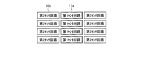
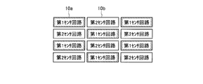
- the arrangement form of the first sensor circuit 10a and the second sensor circuit 10b may be arbitrary.
- two types of sensor circuits may be arranged in the vertical direction.
- two types of sensor circuits may be arranged in a staggered manner.
- the number of two types of sensor circuits may differ.
- the display device of the present invention may perform sensing by the first sensor circuit 10a first, or may perform sensing by the second sensor circuit 10b first.
- reading from the sensor circuit may be performed line by line or may be performed by a plurality of lines.
- sensing by two types of sensor circuits and reading from each sensor circuit may be performed twice or more in one frame period.
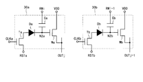
- the display device of the present invention may include a sensor circuit 30 shown in FIG. 15 instead of the sensor circuit 10 shown in FIG.
- the first sensor circuit 30a is obtained by connecting the TFT: Ta and the photodiode Da in reverse order in the first sensor circuit 10a.
- the source of TFT: Ta is connected to the reset terminal, and the drain is connected to the anode of the photodiode Da.
- the cathode of the photodiode Da is connected to the gate of the TFT: Ma.
- the second sensor circuit 30b has the same configuration as the first sensor circuit 30a.
- the sensor circuits 30a and 30b operate in the same manner as the sensor circuits 10a and 10b.
- the display device of the present invention is not limited to one provided with two types of sensor circuits.
- the display device of the present invention may include one type of sensor circuit or may include three or more types of sensor circuits.
- the present invention can be applied to various display devices such as a liquid crystal display device including a liquid crystal panel in which a plurality of optical sensors are two-dimensionally arranged.
- the display devices according to these modified examples have the same effects as the display devices according to the first and second embodiments.
- the display device of the present invention is characterized by low leakage current flowing through the charge holding transistor and high photodetection accuracy, and thus can be used for various display devices including liquid crystal display devices.
Landscapes
- Engineering & Computer Science (AREA)
- General Engineering & Computer Science (AREA)
- Theoretical Computer Science (AREA)
- Human Computer Interaction (AREA)
- Physics & Mathematics (AREA)
- General Physics & Mathematics (AREA)
- Liquid Crystal Display Device Control (AREA)
- Control Of Indicators Other Than Cathode Ray Tubes (AREA)
Abstract
表示装置の画素領域に、リセット線と蓄積ノードの間に光センサと電荷保持トランジスタを設けたセンサ回路を複数個配置する。センシング期間では、リセット線RSTaにリセット解除電圧としてローレベル電圧を印加し、制御線CLKaにハイレベル電圧を印加して電荷保持トランジスタをオン状態に制御する。センシング期間以外では、制御線CLKaにローレベル電圧を印加して電荷保持トランジスタをオフ状態に制御し、リセット線RSTaに保持電圧としてハイレベル電圧を印加する。これにより、電荷保持トランジスタのドレイン・ソース間電圧Vdsを小さくして、電荷保持トランジスタのリーク電流を抑制し、光検出精度を高くする。保持電圧として、リセット電圧と最大光量検知時の蓄積ノードの電圧の略中間の電圧を使用してもよい。
Description
本発明は、表示装置に関し、特に、画素領域に複数の光センサを配置した表示装置に関する。
従来から表示装置に関し、表示パネルに複数の光センサを設け、タッチパネル、ペン入力、スキャナなどの入力機能を提供する方法が知られている。この方法を様々な光環境下で使用されるモバイル機器に適用するためには、光環境の影響を排除する必要がある。そこで、光センサで検知した信号から光環境の影響を受ける成分を除去し、本来入力すべき信号を求める方法も知られている。
そのような方法の1つとして、図16に示すバックライト差分方式が知られている。図16の左側に示すように、バックライト光をシグナル光として使用して、表示パネルの表面近傍にある対象物(例えば、指など)による反射光を光センサで検知する場合、光センサはシグナル光と環境光の両方を検知する。そこで、バックライト差分方式では、バックライトを点灯させた状態とバックライトを消灯させた状態の両方でセンシングを行う。バックライト点灯時のセンシングではシグナル光と環境光が検知され、バックライト消灯時のセンシングでは環境光が検知される。したがって、2つのセンシング結果の差分を求めることにより、シグナル光だけを抽出することができる。バックライト差分方式によれば、光環境に依存しない入力機能を提供することができる。
光センサを動作させるときには、センサ回路に対してリセットと読み出しを行う必要がある。また、所定の期間に入射した光だけを検知する方法として、光センサと直列にトランジスタ(以下、電荷保持トランジスタという)を設け、電荷保持トランジスタをオン/オフ制御する方法がある。センサ回路に対してリセットと読み出しを行うタイミング、および、電荷保持トランジスタをオン/オフ制御するタイミングについては、各種のバリエーションがある。
なお、本願発明に関連して、特許文献1には、光電変換素子、容量素子、および、リセット線と容量素子の間に設けられたスイッチング素子を含むセンサ部を備え、リセット信号をアサートした状態で基準受光信号を読み出し、リセット信号をネゲートしてから所定時間経過後に計測受光信号を読み出す液晶装置が記載されている。
センサ回路内で電荷保持トランジスタは、リセット端子と蓄積ノードの間に光センサと直列に設けられる(後述する図3を参照)。電荷保持トランジスタは、センシング期間ではオン状態に制御され、センシング結果を保持する保持期間ではオフ状態に制御される。しかしながら、保持期間において電荷保持トランジスタをオフ状態に制御しても、電荷保持トランジスタにはリーク電流が流れるので、蓄積ノードに蓄積された電荷の量は変化する。このため、電荷保持トランジスタを含むセンサ回路を備えた表示装置では、センサ回路の出力にノイズが混入し、光検出精度が低下することが問題となる。
この問題は、例えば、センシング期間では光センサに光が入射せず、保持期間では光センサに強い光が入射した場合に顕著になる。この場合、センサ回路の出力は正しくはゼロになるはずである。しかし、電荷保持トランジスタにリーク電流が流れると、センサ回路の出力はゼロにならない。また、この問題は、センサ回路ごとに保持期間の長さが異なる場合にも顕著になる(後述する図7の説明を参照)。
それ故に、本発明は、電荷保持トランジスタを流れるリーク電流を抑制し、光検出精度が高い表示装置を提供することを目的とする。
本発明の第1の局面は、画素領域に複数の光センサを配置した表示装置であって、
複数の画素回路および複数のセンサ回路を含む表示パネルと、
前記画素回路および前記センサ回路を駆動する駆動回路とを備え、
前記センサ回路は、
検知した光量に応じた電荷を蓄積する蓄積ノードと、
前記蓄積ノードと前記駆動回路によって制御されるリセット線との間に設けられた光センサと、
前記光センサと直列に設けられ、前記駆動回路によってオン/オフ制御される電荷保持トランジスタとを含み、
前記駆動回路は、前記電荷保持トランジスタをオフ状態に制御する間、前記電荷保持トランジスタの導通端子間の電圧を小さくするための保持電圧を前記リセット線に印加することを特徴とする。
複数の画素回路および複数のセンサ回路を含む表示パネルと、
前記画素回路および前記センサ回路を駆動する駆動回路とを備え、
前記センサ回路は、
検知した光量に応じた電荷を蓄積する蓄積ノードと、
前記蓄積ノードと前記駆動回路によって制御されるリセット線との間に設けられた光センサと、
前記光センサと直列に設けられ、前記駆動回路によってオン/オフ制御される電荷保持トランジスタとを含み、
前記駆動回路は、前記電荷保持トランジスタをオフ状態に制御する間、前記電荷保持トランジスタの導通端子間の電圧を小さくするための保持電圧を前記リセット線に印加することを特徴とする。
本発明の第2の局面は、本発明の第1の局面において、
前記駆動回路は、前記リセット線に前記保持電圧としてリセット電圧を印加することを特徴とする。
前記駆動回路は、前記リセット線に前記保持電圧としてリセット電圧を印加することを特徴とする。
本発明の第3の局面は、本発明の第1の局面において、
前記駆動回路は、前記リセット線に前記保持電圧として、リセット電圧とリセット解除電圧との間にある電圧を印加することを特徴とする。
前記駆動回路は、前記リセット線に前記保持電圧として、リセット電圧とリセット解除電圧との間にある電圧を印加することを特徴とする。
本発明の第4の局面は、本発明の第3の局面において、
前記駆動回路は、前記リセット線に前記保持電圧として、前記リセット電圧および最大光量検知時の前記蓄積ノードの電圧の略中間の電圧を印加することを特徴とする。
前記駆動回路は、前記リセット線に前記保持電圧として、前記リセット電圧および最大光量検知時の前記蓄積ノードの電圧の略中間の電圧を印加することを特徴とする。
本発明の第5の局面は、本発明の第1の局面において、
所定の周期で点灯および消灯する光源をさらに備え、
前記センサ回路は第1センサ回路および第2センサ回路を含み、
前記駆動回路は、前記光源が消灯している間に前記第1センサ回路内の電荷保持トランジスタをオン状態に制御し、前記光源が点灯している間に前記第2センサ回路内の電荷保持トランジスタをオン状態に制御することを特徴とする。
所定の周期で点灯および消灯する光源をさらに備え、
前記センサ回路は第1センサ回路および第2センサ回路を含み、
前記駆動回路は、前記光源が消灯している間に前記第1センサ回路内の電荷保持トランジスタをオン状態に制御し、前記光源が点灯している間に前記第2センサ回路内の電荷保持トランジスタをオン状態に制御することを特徴とする。
本発明の第6の局面は、本発明の第5の局面において、
前記駆動回路は、前記第1および第2センサ回路内の電荷保持トランジスタをすべてオフ状態に制御しながら、前記第1および第2センサ回路からの読み出しを線順次で行うことを特徴とする。
前記駆動回路は、前記第1および第2センサ回路内の電荷保持トランジスタをすべてオフ状態に制御しながら、前記第1および第2センサ回路からの読み出しを線順次で行うことを特徴とする。
本発明の第7の局面は、本発明の第6の局面において、
前記駆動回路は、前記第1センサ回路からの読み出しと前記第2センサ回路からの読み出しとを並列に行うことを特徴とする。
前記駆動回路は、前記第1センサ回路からの読み出しと前記第2センサ回路からの読み出しとを並列に行うことを特徴とする。
本発明の第8の局面は、本発明の第1の局面において、
前記光センサの一端は前記リセット線に接続され、他端は前記電荷保持トランジスタの一方の導通端子に接続され、前記電荷保持トランジスタの他方の導通端子は前記蓄積ノードに接続されていることを特徴とする。
前記光センサの一端は前記リセット線に接続され、他端は前記電荷保持トランジスタの一方の導通端子に接続され、前記電荷保持トランジスタの他方の導通端子は前記蓄積ノードに接続されていることを特徴とする。
本発明の第9の局面は、本発明の第8の局面において、
前記センサ回路は、前記蓄積ノードに接続された制御端子を有する読み出しトランジスタをさらに含むことを特徴とする。
前記センサ回路は、前記蓄積ノードに接続された制御端子を有する読み出しトランジスタをさらに含むことを特徴とする。
本発明の第10の局面は、本発明の第9の局面において、
前記センサ回路は、前記蓄積ノードと前記駆動回路によって制御される読み出し線との間に設けられたコンデンサをさらに含むことを特徴とする。
前記センサ回路は、前記蓄積ノードと前記駆動回路によって制御される読み出し線との間に設けられたコンデンサをさらに含むことを特徴とする。
本発明の第1の局面によれば、保持期間においてリセット線に保持電圧を印加することにより、電荷保持トランジスタの導通端子間の電圧を小さくし、電荷保持トランジスタに流れるリーク電流を抑制することができる。したがって、保持期間における蓄積ノードの電圧の変化を抑制し、光検出精度を高くすることができる。
本発明の第2の局面によれば、保持電圧としてリセット電圧を用いることにより、新たな電圧を生成することなく、電荷保持トランジスタの導通端子間の電圧を小さくし、電荷保持トランジスタに流れるリーク電流を抑制することができる。したがって、簡単な回路で光検出精度を高くすることができる。
本発明の第3の局面によれば、保持電圧としてリセット電圧とリセット解除電圧との間にある好適な電圧を用いることにより、電荷保持トランジスタの導通端子間の電圧をより小さくし、電荷保持トランジスタに流れるリーク電流をさらに抑制することができる。したがって、好適な電圧を用いて光検出精度をさらに高くすることができる。
本発明の第4の局面によれば、保持電圧としてリセット電圧と最大光量検知時の蓄積ノードの電圧の略中間の電圧を用いることにより、電荷保持トランジスタの導通端子間の電圧をより小さくて、電荷保持トランジスタに流れるリーク電流をさらに抑制することができる。したがって、好適な電圧を用いて光検出精度をさらに高くすることができる。
本発明の第5の局面によれば、2種類のセンサ回路を用いて光源消灯時の光量と光源点灯時の光量を別個に検知し、センサ回路の外部で両者の差を求めることができる。したがって、光源からの出射光をシグナル光として使用して、光環境に依存しない入力機能を提供することができる。
本発明の第6の局面によれば、センサ回路によるセンシングとセンサ回路からの読み出しを異なる期間で行うことにより、センシングおよび読み出しタイミングを決定するときの自由度を大きくすることができる。
本発明の第7の局面によれば、第1センサ回路からの読み出しと第2センサ回路からの読み出しとを並列に行うことにより、読み出し速度を遅くして、表示装置の消費電力を削減することができる。
本発明の第8の局面によれば、光センサと電荷保持トランジスタを直列に接続し、その一端をリセット線に接続し、他端を蓄積ノードに接続することにより、所定の期間に入射した光だけを検知するセンサ回路を構成することができる。
本発明の第9の局面によれば、センサ回路に読み出しトランジスタを設け、読み出しトランジスタの一方の導通端子に所定の電圧を印加することにより、読み出しトランジスタの他方の導通端子から蓄積ノードの電圧に応じた信号を出力し、検知した光量に応じた信号をセンサ回路から読み出すことができる。
本発明の第10の局面によれば、センサ回路にコンデンサを設け、読み出し線に読み出し電圧を印加することにより、蓄積ノードの電圧を変化させ、検知した光量に応じた信号をセンサ回路から読み出すことができる。
(第1の実施形態)
図1は、本発明の第1の実施形態に係る表示装置の構成を示すブロック図である。図1に示す表示装置は、表示制御回路1、表示パネル2、および、バックライト3を備えている。表示パネル2は、画素領域4、ゲートドライバ回路5、ソースドライバ回路6、センサロウドライバ回路7、および、センサカラムドライバ回路8を含んでいる。画素領域4は、複数の画素回路9と複数のセンサ回路10を含んでいる。この表示装置は、表示パネル2に画像を表示する機能と、表示パネル2に入射した光を検知する機能とを有する。以下、mおよびnは偶数、iはm以下の偶数、jは2n以下の偶数であるとし、表示装置のフレームレートを60フレーム/秒とする。
図1は、本発明の第1の実施形態に係る表示装置の構成を示すブロック図である。図1に示す表示装置は、表示制御回路1、表示パネル2、および、バックライト3を備えている。表示パネル2は、画素領域4、ゲートドライバ回路5、ソースドライバ回路6、センサロウドライバ回路7、および、センサカラムドライバ回路8を含んでいる。画素領域4は、複数の画素回路9と複数のセンサ回路10を含んでいる。この表示装置は、表示パネル2に画像を表示する機能と、表示パネル2に入射した光を検知する機能とを有する。以下、mおよびnは偶数、iはm以下の偶数、jは2n以下の偶数であるとし、表示装置のフレームレートを60フレーム/秒とする。
図1に示す表示装置には外部から、映像信号Vinとタイミング制御信号Cinが供給される。表示制御回路1は、これらの信号に基づき、表示パネル2に対して映像信号VSと制御信号CSg、CSs、CSrを出力し、バックライト3に対して制御信号CSbを出力する。映像信号VSは、映像信号Vinと同じでもよく、映像信号Vinに信号処理を施した信号でもよい。
バックライト3は、表示パネル2に光を照射する光源である。より詳細には、バックライト3は、表示パネル2の背面側に設けられ、表示パネル2の背面に光を照射する。バックライト3は、制御信号CSbがハイレベルのときには点灯し、制御信号CSbがローレベルのときには消灯する。バックライト3は、例えば、赤外光を出射する赤外LED(Light Emitting Diode)を用いて構成される。
表示パネル2の画素領域4には、(m×3n)個の画素回路9と(m×n)個のセンサ回路10が、それぞれ2次元状に配置される。より詳細には、画素領域4には、m本のゲート線GL1~GLmと3n本のソース線SL1~SL3nが設けられる。ゲート線GL1~GLmは互いに平行に配置され、ソース線SL1~SL3nはゲート線GL1~GLmと直交するように互いに平行に配置される。(m×3n)個の画素回路9は、ゲート線GL1~GLmとソース線SL1~SL3nの各交点近傍に配置される。各画素回路9は、1本のゲート線GLと1本のソース線SLに接続される。画素回路9は、赤色表示用、緑色表示用および青色表示用に分類される。これら3種類の画素回路9は、ゲート線GL1~GLmの伸延方向に並べて配置され、1個のカラー画素を構成する。
画素領域4には、ゲート線GL1~GLmと平行に、m本の制御線CLK1~CLKm、m本のリセット線RST1~RSTm、および、m本の読み出し線RW1~RWmが設けられる。また、画素領域4には、ソース線SL1~SL3nと平行に、2n本の出力線OUT1~OUT2nが設けられる。さらに画素領域4には、所定の電源電圧が固定的に印加された電源線VDDが設けられる。(m×n)個のセンサ回路10は、奇数番目の読み出し線RW1、RW3、…と奇数番目の出力線OUT1、OUT3、…の各交点近傍、および、偶数番目の読み出し線RW2、RW4、…と偶数番目の出力線OUT2、OUT4、…の各交点近傍に配置される。各センサ回路10は、1本の制御線CLK、1本のリセット線RST、1本の読み出し線RW、1本の出力線OUT、および、電源線VDDに接続される。
ゲートドライバ回路5、ソースドライバ回路6、センサロウドライバ回路7、および、センサカラムドライバ回路8は、画素回路9およびセンサ回路10を駆動する駆動回路として機能する。ゲートドライバ回路5は、画素領域4の一辺(図1では右辺)に沿って配置される。センサロウドライバ回路7は、画素領域4の対向する辺(図1では左辺)に沿って配置される。ソースドライバ回路6とセンサカラムドライバ回路8は、表示領域の他の一辺(図1では上辺)に沿って配置される。これらの駆動回路は、画素回路9およびセンサ回路10と共に表示パネル2上にモノリシックに形成されていてもよく、表示パネル2上に実装されたICチップに内蔵されていてもよい。
ゲートドライバ回路5は、制御信号CSgに基づき、ゲート線GL1~GLmを駆動する。より詳細には、ゲートドライバ回路5は、制御信号CSgに基づき、ゲート線GL1~GLmの中から1本のゲート線を順に選択し、選択したゲート線にハイレベル電圧を、残りのゲート線にローレベル電圧を印加する。これにより、選択されたゲート線に接続された3n個の画素回路9が、一括して選択される。
ソースドライバ回路6は、制御信号CSsに基づき、ソース線SL1~SL3nを駆動する。より詳細には、ソースドライバ回路6は、制御信号CSsに基づき、映像信号VSに応じた電圧をソース線SL1~SL3nに印加する。このときソースドライバ回路6は、線順次駆動を行ってもよく、点順次駆動を行ってもよい。ソース線SL1~SL3nに印加された電圧は、ゲートドライバ回路5によって選択された3n個の画素回路9に書き込まれる。このようにゲートドライバ回路5とソースドライバ回路6を用いてすべての画素回路9に映像信号VSに応じた電圧を書き込むことにより、表示パネル2に所望の画像を表示することができる。
センサロウドライバ回路7は、制御信号CSrに基づき、制御線CLK1~CLKm、リセット線RST1~RSTm、および、読み出し線RW1~RWmを駆動する(詳細は後述)。センサロウドライバ回路7は、制御信号CSrに基づき第1センシング期間において、偶数番目のリセット線にローレベル電圧を印加しながら、偶数番目の制御線にハイレベル電圧を印加する。次に、センサロウドライバ回路7は、第2センシング期間において、奇数番目のリセット線にローレベル電圧を印加しながら、奇数番目の制御線にハイレベル電圧を印加する。センサ回路10は、リセット線RSTにローレベル電圧が印加され、制御線CLKにハイレベル電圧が印加されているときに入射した光を検知する。その後、センサロウドライバ回路7は、制御信号CSrに基づき、読み出し線RW1~RWmの中から隣接した2本の読み出し線を順に選択し、選択した読み出し線にハイレベル電圧を印加する。これにより、選択された読み出し線に接続された2n個のセンサ回路10から出力線OUT1~OUT2nに2n個の信号が出力される。
センサカラムドライバ回路8は、奇数行目のセンサ回路10の出力信号と偶数行目のセンサ回路10の出力信号の差を求める差分回路(図示せず)を含んでいる。センサカラムドライバ回路8は、差分回路で求めた信号の差を増幅し、増幅後の信号をセンサ出力Soutとして表示パネル2の外部に出力する。このようにセンサロウドライバ回路7とセンサカラムドライバ回路8を用いてすべてのセンサ回路10から信号を読み出すことにより、表示パネル2に入射した光を検知することができる。
図2は、センサ回路10の配置、および、センサロウドライバ回路7の構成を示す図である。図2に示すように、(m×n)個のセンサ回路10は、バックライト3の消灯期間に入射した光を検知する第1センサ回路10aと、バックライト3の点灯期間に入射した光を検知する第2センサ回路10bとに分類される。第1センサ回路10aと第2センサ回路10bは同数である。(m×n/2)個の第1センサ回路10aは偶数行目に配置され、(m×n/2)個の第2センサ回路10bは奇数行目に配置される。
奇数番目の制御線CLK1、CLK3、…は、いずれも制御線CLKbに接続される。偶数番目の制御線CLK2、CLK4、…は、いずれも制御線CLKaに接続される。奇数番目のリセット線RST1、RST3、…は、いずれもリセット線RSTbに接続される。偶数番目のリセット線RST2、RST4、…は、いずれもリセット線RSTaに接続される。第1センサ回路10aは、偶数番目の制御線を介して制御線CLKaに接続され、偶数番目のリセット線を介してリセット線RSTaに接続される。第2センサ回路10bは、奇数番目の制御線を介して制御線CLKbに接続され、奇数番目のリセット線を介してリセット線RSTbに接続される。
センサロウドライバ回路7は、m段のシフトレジスタ11を含んでいる。シフトレジスタ11は、1段目に入力されたパルス信号RWSPをクロック信号RWCKに基づき順にシフトする。シフトレジスタ11の各段から出力される信号は、順にハイレベルになる。シフトレジスタ11から出力されたm個の信号は、読み出し線RW1~RWmにそれぞれ与えられる。
図3は、センサ回路10の回路図である。図3に示すように、第1センサ回路10aは、TFT(Thin Film Transistor):Ta、Ma、フォトダイオードDa、および、コンデンサCaを含んでいる。第2センサ回路10bは、TFT:Tb、Mb、フォトダイオードDb、および、コンデンサCbを含んでいる。TFT:Ta、Ma、Tb、Mbは、いずれもNチャネル型TFTである。フォトダイオードDa、Dbは光センサとして機能し、TFT:Ta、Tbは電荷保持トランジスタとして機能し、TFT:Ma、Mbは読み出しトランジスタとして機能する。
第1センサ回路10aでは、フォトダイオードDaのアノードはリセット端子に接続され、カソードはTFT:Taのソースに接続される。TFT:Taのゲートは制御端子に接続され、ドレインはTFT:Maのゲートに接続される。TFT:Maのドレインは電源端子に接続され、ソースは出力端子に接続される。コンデンサCaは、TFT:Maのゲートと読み出し端子との間に設けられる。以下、フォトダイオードDaとTFT:Taが接続されたノードをノードN1aといい、TFT:Ta、MaとコンデンサCaが接続されたノードをノードN2aという。ノードN2aは、検知した光量に応じた電荷を蓄積する蓄積ノードとして機能する。
第1センサ回路10aの制御端子は、偶数番目の制御線を介して制御線CLKaに接続される。リセット端子は、偶数番目のリセット線を介してリセット線RSTaに接続される。読み出し端子は、偶数番目の読み出し線RWiに接続される。出力端子は、偶数番目の出力線OUTjに接続される。電源端子は、電源線VDDに接続される。
第2センサ回路10bは、第1センサ回路10aと同じ構成を有する。ただし、第2センサ回路10bの制御端子は、奇数番目の制御線を介して制御線CLKbに接続される。リセット端子は、奇数番目のリセット線を介してリセット線RSTbに接続される。読み出し端子は、奇数番目の読み出し線RWi-1に接続される。出力端子は、奇数番目の出力線OUTj-1に接続される。
図4は、バックライト3の点灯および消灯タイミング、並びに、センサ回路10に対するリセットおよび読み出しタイミングを示す図である。バックライト3は、1フレーム期間に1回、所定時間だけ点灯し、それ以外の期間では消灯する。具体的には、バックライト3は、1フレーム期間内の時刻tbにおいて点灯し、時刻tcにおいて消灯する。このようにバックライト3は、所定の周期で点灯および消灯する。
第1センサ回路10aは、時刻taから時刻tbまでの第1センシング期間A1(バックライト3の消灯時のセンシング期間)に入射した光を検知する。第2センサ回路10bは、時刻tbから時刻tcまでの第2センシング期間A2(バックライト3の点灯時のセンシング期間)に入射した光を検知する。第1センシング期間A1と第2センシング期間A2の長さは同じである。第1センシング期間A1以外では第1センサ回路10aに対するリセットが継続的に行われ、第2センシング期間A2以外では第2センサ回路10bに対するリセットが継続的に行われる。第1センサ回路10aからの読み出しと第2センサ回路10bからの読み出しは、時刻tc以降に並列に線順次で行われる。
図5は、表示パネル2の信号波形図である。以下、信号線上の信号を識別するために、信号線と同じ名称を使用する(例えば、制御線CLKa上の信号を制御信号CLKaという)。図5に示すように、ゲート信号GL1~GLmは、1フレーム期間に1回ずつ順に所定時間ずつハイレベルになる。制御信号CLKaは、1フレーム期間に1回、第1センシング期間A1において(より詳細には、時刻taから時刻tbの少し前まで)ハイレベルになり、それ以外ではローレベルになる。制御信号CLKbは、1フレーム期間に1回、第2センシング期間A2において(より詳細には、時刻tbから時刻tcの少し前まで)ハイレベルになり、それ以外ではローレベルになる。リセット信号RSTaは、第1センシング期間A1において(より詳細には、時刻taの少し後から時刻tbの少し前まで)ローレベルになり、それ以外ではハイレベルになる。リセット信号RSTbは、第2センシング期間A2において(より詳細には、時刻tbの少し後から時刻tcの少し前まで)ローレベルになり、それ以外ではハイレベルになる。読み出し信号RW1~RWmは2本ずつ対にされ、(m/2)対の読み出し信号は時刻tc以降に順に所定時間ずつハイレベルになる。
図6は、第1センサ回路10aの信号波形図である。図6には、ノードN1a、N2aの電圧の変化が記載されている。図6では、時刻taから時刻t2までがリセット期間、時刻t2から時刻t3までがセンシング期間、時刻t4から時刻t5までが保持期間、時刻t5から時刻t6までが読み出し期間となる。制御信号CLKaは、リセット期間とセンシング期間ではハイレベルになり、それ以外ではローレベルになる。リセット信号RSTaは、センシング期間と時刻t3から時刻t4までの期間ではローレベルになり、それ以外ではハイレベルになる。読み出し信号RWiは、読み出し期間ではハイレベルになり、それ以外ではローレベルになる。
リセット期間(時刻ta~t2)では、制御信号CLKaとリセット信号RSTaはハイレベルになり、読み出し信号RWiはローレベルになる。このとき、TFT:Taはオン状態である。したがって、リセット線RSTaからフォトダイオードDaとTFT:Taを経由してノードN2aに電流(フォトダイオードDaの順方向電流)が流れ、ノードN2aの電圧はハイレベルにリセットされる。
センシング期間(時刻t2~t3)では、制御信号CLKaはハイレベルのまま、読み出し信号RWiはローレベルのままで、リセット信号RSTaがローレベルになる。センシング期間では、TFT:Taは引き続きオン状態である。このため、フォトダイオードDaに光が入射すると、ノードN2aからTFT:TaとフォトダイオードDaを経由してリセット線RSTaに電流(フォトダイオードDaのフォト電流)が流れ、ノードN2aから電荷が引き抜かれる。したがって、ノードN2aの電圧は、センシング期間(バックライト3の消灯時のセンシング期間)に入射した光の量に応じて下降する。なお、リセット期間およびセンシング期間では、TFT:Taがオン状態であるので、ノードN1aの電圧はノードN2aの電圧に等しい。
時刻t3において、制御信号CLKaがローレベルになる。時刻t3以降、TFT:Taはオフ状態になり、ノードN1a、N2aは電気的に切り離される。
保持期間(時刻t4~t5)では、制御信号CLKaと読み出し信号RWiはローレベルのままで、リセット信号RSTaがハイレベルになる。保持期間では、TFT:Taはオフ状態であり、ノードN1a、N2aは電気的に切り離されている。このため、フォトダイオードDaに光が入射しても、ノードN2aの電圧は変化しない。一方、ノードN1aの電圧は、ハイレベルにリセットされる(図6の太破線を参照)。保持期間では、TFT:Taのドレイン・ソース間電圧Vdsは、ノードN1aの電圧とノードN2aの電圧の差となる。
読み出し期間(時刻t5~t6)では、制御信号CLKaはローレベルのまま、リセット信号RSTaはハイレベルのままで、読み出し信号RWiがハイレベルになる。読み出し期間では、TFT:Taは引き続きオフ状態である。このときノードN2aの電圧は、読み出し信号RWiの電圧の上昇量の所定倍(乗数はコンデンサCaの容量値と第1センサ回路10aの全体の容量値の比によって定まる)だけ上昇する。TFT:Maは、センサカラムドライバ回路8に含まれるトランジスタ(図示せず)を負荷としたソースフォロワ増幅回路を構成し、ノードN2aの電圧に応じて出力線OUTaを駆動する。
このように第1センサ回路10aは、第1センシング期間A1(バックライト3の消灯時のセンシング期間)に入射した光の量に応じた信号を出力する。第2センサ回路10bは、第1センサ回路10aと同様に動作し、第2センシング期間A2(バックライト3の点灯時のセンシング期間)に入射した光の量に応じた信号を出力する。したがって、センサカラムドライバ回路8に含まれる差分回路を用いて、第1センサ回路10aの出力信号と第2センサ回路10bの出力信号の差を求めることにより、バックライト点灯時の光量とバックライト消灯時の光量の差を求めることができる。
本実施形態に係る表示装置は、TFT:Ta、Tbをオフ状態に制御する間(すなわち、センシング期間以外では)、TFT:Ta、Tbのドレイン・ソース間電圧Vdsを小さくするための保持電圧をリセット線RSTa、RSTbに印加する。本実施形態に係る表示装置は、センシング期間以外では、保持電圧としてハイレベル電圧(リセット電圧)をリセット線RSTに印加する。以下、センシング期間以外ではリセット線RSTにローレベル電圧(リセット解除電圧)を印加する表示装置(以下、参考例に係る表示装置という)と対比して、本実施形態に係る表示装置の効果を説明する。
図7および図8は、参考例に係る表示装置の信号波形図である。参考例に係る表示装置では、図7に示すように、リセット信号RSTaは、第1センシング期間の一部で(より詳細には、時刻taの少し後から所定時間だけ)ハイレベルになり、それ以外ではローレベルになる。リセット信号RSTbは、第2センシング期間A2の一部で(より詳細には、時刻tbの少し後から所定時間だけ)ハイレベルになり、それ以外ではローレベルになる。図8に示すように、リセット信号RSTaは、リセット期間(時刻t1~t2)においてのみハイレベルになる。
図9は、フォトダイオードのI-V特性を示す図である。図9には、入射光量をX1~X3(ただし、X1<X2<X3)の3段階に切り替えたときのI-V特性が記載されている。図9において、横軸はフォトダイオードに印加されるバイアス電圧Vacを表し、縦軸はフォトダイオードを流れる電流Iの絶対値を表す。負のバイアス電圧Vacが印加されたとき、フォトダイオードには逆方向電流が流れる。バイアス電圧Vacが図9に示す範囲R(V2~V1の範囲)内にあるとき、逆方向電流はほぼ一定になる。フォトダイオードは、バイアス電圧Vacが変化しても電流が変化せず、入射光量が変化すると電流が線形に変化する条件下で使用することが好ましい。そこで、図9に示すI-V特性を有するフォトダイオードを使用するときには、範囲R内のバイアス電圧Vacを印加する。なお、電圧V1、V2の値は、製造プロセスやデバイス構造によって異なる。
図3に示す第1センサ回路10aにおいてハイレベル電圧をリセット電圧とする場合、リセット直後のバイアス電圧の絶対値|Vac|が|V2|以下となるように(Vac>V2となるように)、リセット信号RSTaのローレベル電圧が決定される。センシング期間では、ノードN2aの電圧が徐々に低下し、バイアス電圧の絶対値|Vac|は徐々に小さくなる。フォトダイオードを正しく動作させるためには、センシング期間にフォトダイオードに最大の光が入射したときに、センシング期間終了時のバイアス電圧の絶対値|Vac|が|V1|以上となるように(Vac<V1となるように)、センシング期間の長さなどが決定される。
具体例を挙げて説明する。以下では、リセット信号のローレベル電圧を-5V、リセット信号のハイレベル電圧を0Vとし、フォトダイオードに-5V以上-2V以下のバイアス電圧Vacを印加する場合を考える。この場合、ノードN1aの電圧は-5V~0Vの範囲で変化し、ノードN2aの電圧は-3V~0Vの範囲で変化する。
参考例に係る表示装置では、上記条件(RST=-5V/0V、Vac=-5V~-2V)下において、TFT:Taを流れるリーク電流が最大になるのは、ノードN1aの電圧が-5VでノードN2aの電圧が0Vのときである。このとき、TFT:Taのドレイン・ソース間電圧の絶対値|Vds|は5Vとなる。したがって、|Vds|=5Vに対応したリーク電流がTFT:Ta、Tbを流れる。このため、参考例に係る表示装置では、5Vに対応したリーク電流によるノイズがセンサ回路の出力に混入し、その分だけ光検出精度が低下する。
図7に示す信号波形図では、第1センサ回路10aによるセンシングと第2センサ回路10bによるセンシングとは、異なる期間で行われる。また、センサ回路10からの読み出しは線順次で行われるので、最初に読み出しが行われるセンサ回路10と最後に読み出しが行われるセンサ回路10では、保持期間の長さが異なる。このため、最初に読み出しが行われる第1センサ回路10aの保持期間をH1、最初に読み出しが行われる第2センサ回路10bの保持期間をH2、最後に読み出しが行われる第1センサ回路10aの保持期間をH3、最後に読み出しが行われる第2センサ回路10bの保持期間をH4としたとき、4つの保持期間の長さはすべて異なる。このようにセンサ回路ごとに保持期間の長さが異なる場合には、TFT:Ta、Tbを流れるリーク電流によって、センサ回路の出力に保持期間の長さの違いに起因するばらつきが生じ、光検出精度が低下する。
本実施形態に係る表示装置は、TFT:Taをオフ状態に制御する間、TFT:Taのドレイン・ソース間電圧Vdsを小さくするための保持電圧としてハイレベル電圧をリセット線RSTに印加する。このため、上記条件(RST=-5V/0V、Vac=-5V~-2V)下において、TFT:Taを流れるリーク電流が最大になるのは、ノードN1aの電圧が0VでノードN2aの電圧が-3Vのときである。このとき、TFT:Taのドレイン・ソース間電圧の絶対値|Vds|は3Vとなる。この値は、参考例に係る表示装置よりも小さい。したがって、本実施形態に係る表示装置によれば、TFT:Taをオフ状態に制御する間、保持電圧としてハイレベル電圧をリセット線RSTに印加することにより、TFT:Taを流れるリーク電流を抑制して、光検出精度を高くすることができる。
以上に示すように、本実施形態に係る表示装置は、電荷保持トランジスタ(TFT:Ta、Tb)がオフ状態であるときに、電荷保持トランジスタの導通端子間(TFT:Ta、Tbのドレイン・ソース間)の電圧を小さくするための保持電圧をリセット線RSTa、RSTbに印加する。これにより、電荷保持トランジスタの導通端子間の電圧を小さくし、電荷保持トランジスタに流れるリーク電流を抑制することができる。したがって、検知した光量に応じた電荷を蓄積ノードに高い精度で蓄積し、光センサの検出精度を高くすることができる。特に、保持電圧としてリセット電圧(ハイレベル電圧)を用いることにより、新たな電圧を生成することなく、電荷保持トランジスタの導通端子間の電圧を小さくし、電荷保持トランジスタに流れるリーク電流を抑制することができる。したがって、簡単な回路で光センサの検出精度を高くすることができる。
また、2種類のセンサ回路10a、10bを用いて光源(バックライト3)消灯時の光量と光源点灯時の光量を別個に検知し、センサ回路10a、10bの外部で両者の差を求めることができる。これにより、光源からの出射光をシグナル光として使用して、光環境に依存しない入力機能を提供することができる。また、2種類のセンサ回路10a、10bに対するセンシングと読み出しを別の期間で行うことにより、センシングおよび読み出しタイミングを決定するときの自由度を大きくすることができる。また、第1センサ回路10aからの読み出しと第2センサ回路10bからの読み出しとを並列に行うことにより、読み出し速度を遅くして、表示装置の消費電力を削減することができる。
また、光センサ(フォトダイオードDa)と電荷保持トランジスタ(TFT:Ta)を直列に接続し、その一端をリセット線RSTaに接続し、他端を蓄積ノード(ノードN2a)に接続することにより、所定の期間に入射した光だけを検知するセンサ回路を構成することができる。また、センサ回路に読み出しトランジスタ(TFT:Ma)を設け、読み出しトランジスタの一方の導通端子(ドレイン端子)に電源電圧VDDを印加することにより、読み出しトランジスタの他方の導通端子(ソース端子)から蓄積ノードの電圧に応じた信号を出力し、検知した光量に応じた信号をセンサ回路から読み出すことができる。また、センサ回路にコンデンサ(コンデンサCa)を設け、読み出し線RWiに読み出し電圧(ハイレベル電圧)を印加することにより、蓄積ノードの電圧を変化させ、検知した光量に応じた信号をセンサ回路から読み出すことができる。
(第2の実施形態)
本発明の第2の実施形態に係る表示装置は、第1の実施形態に係る表示装置と同じ構成を有し、同じ画素回路を備えている(図1および図3を参照)。本実施形態は、リセット線に印加する保持電圧のレベルが第1の実施形態と相違する。以下、第1の実施形態との相違点を説明する。
本発明の第2の実施形態に係る表示装置は、第1の実施形態に係る表示装置と同じ構成を有し、同じ画素回路を備えている(図1および図3を参照)。本実施形態は、リセット線に印加する保持電圧のレベルが第1の実施形態と相違する。以下、第1の実施形態との相違点を説明する。
図10は、本実施形態に係る表示装置におけるセンサ回路10の配置、および、センサロウドライバ回路7の構成を示す図である。本実施形態では、奇数番目のリセット線RST1、RST3、…は、いずれもリセット線RSTObに接続される。偶数番目のリセット線RST2、RST4、…は、いずれもリセット線RSTOaに接続される。センサロウドライバ回路7は、リセット信号RSTOaを出力するリセット制御回路20a、および、リセット線RSTObを出力するリセット制御回路20bを含んでいる。
図11は、リセット制御回路20aの回路図である。図11に示すように、リセット制御回路20aは、4個のアナログスイッチ21~24を含んでいる。リセット制御回路20aには、制御信号CLKa、HOLBa、リセット信号RSTa、ハイレベル電圧RST_High、ローレベル電圧RST_Low、および、中間電圧Vmが入力される。リセット信号RSTaがローレベルのときには、アナログスイッチ23はオン状態、アナログスイッチ24はオフ状態になり、リセット信号RSTaの電圧はローレベル電圧RST_Lowに等しくなる。リセット信号RSTaがハイレベルで、制御信号CLKa、HOLBaの少なくとも一方がハイレベルのときには、アナログスイッチ21、24はオン状態、アナログスイッチ22、23はオフ状態になり、リセット信号RSTOaの電圧はハイレベル電圧RST_Highに等しくなる。リセット信号RSTaがハイレベルで、制御信号CLKa、HOLBaが共にローレベルのときには、アナログスイッチ22、24はオン状態、アナログスイッチ21、23はオフ状態になり、リセット信号RSTOaの電圧は中間電圧Vmに等しくなる。リセット制御回路20bは、リセット制御回路20aと同じ構成を有する。
図12および図13は、本実施形態に係る表示装置の信号波形図である。本実施形態に係る表示装置では、図12に示すように、リセット信号RSTaは、第1センシング期間の先頭部分で(より詳細には、時刻taから所定時間だけ)ハイレベルになり、第1センシング期間の残部で(より詳細には、時刻taから所定時間経過後から時刻tbの少し前まで)ローレベルになり、それ以外では中間レベル(中間電圧Vm)になる。リセット信号RSTbは、第2センシング期間の先頭部分で(より詳細には、時刻tbから所定時間だけ)ハイレベルになり、第2センシング期間の残部で(より詳細には、時刻tbから所定時間経過後から時刻tcの少し前まで)ローレベルになり、それ以外では中間レベルになる。図13に示すように、リセット信号RSTaは、リセット期間(時刻ta~t2)ではハイレベル、センシング期間(時刻t2~t3)と時刻t3から時刻t4までの期間ではローレベルになり、それ以外では中間レベルになる。
中間電圧Vmには、リセット電圧(ハイレベル電圧)とリセット解除電圧(ローレベル電圧)との間にある電圧が使用される。例えば、中間電圧Vmとして、ハイレベル電圧と最大光量検知時のノードN2aの電圧の略中間の電圧を使用することができる。上記条件(RST=-5V/0V、Vac=-5V~-2V)下では、最大光量検知時のノードN2aの電圧は-3Vとなる。この場合、中間電圧Vmとして、0V(ハイレベル電圧)と-3Vの中間の電圧である-1.5V(あるいは、-1.5Vに略等しい電圧)を使用することができる。
上記条件下で中間電圧Vmを-1.5Vに設定した場合、TFT:Taを流れるリーク電流が最大になるのは、ノードN1aの電圧が-1.5VでノードN2aの電圧が0Vのとき、および、ノードN1aの電圧が-1.5VでノードN2aの電圧が-3Vのときである。いずれのときでも、TFT:Taのドレイン・ソース間電圧の絶対値|Vds|は1.5Vとなる。この値は、参考例に係る表示装置よりも小さく、第1の実施形態に係る表示装置よりも小さい。したがって、本実施形態に係る表示装置によれば、TFT:Taをオフ状態に制御する間、保持電圧としてハイレベル電圧と最大光量検知時の蓄積ノードの電圧の中間電圧をリセット線RSTに印加することにより、TFT:Taのドレイン・ソース間電圧Vdsをより小さくして、TFT:Taを流れるリーク電流をさらに抑制して、光検出精度をさらに高くすることができる。
以上に示すように、本実施形態に係る表示装置によれば、保持電圧としてリセット電圧(ハイレベル電圧)およびリセット解除電圧(ローレベル電圧)の間にある電圧を用いることにより、電荷保持トランジスタの導通端子間の電圧(TFT:Ma、Mbのドレイン・ソース間電圧)をより小さくし、電荷保持トランジスタに流れるリーク電流をさらに抑制することができる。したがって、光センサの検出精度をさらに高くすることができる。特に、保持電圧として、リセット電圧と最大光量検知時の蓄積ノードの電圧の略中間の電圧を使用することが効果的である。
なお、本発明の表示装置については、各種の変形例を構成することができる。例えば、画素領域4に設けるセンサ回路10の個数や読み出し線の本数は任意でよい。例えば、m本の読み出し線とn本の出力線の各交点近傍に、全部で(m×n)個のセンサ回路10を配置してもよい。あるいは、複数のカラー画素に対応して、センサ回路10を設けてもよい。また、第1センサ回路10aと第2センサ回路10bの配置形態は任意でよい。例えば、図14Aに示すように、2種類のセンサ回路をそれぞれ縦方向に並べて配置してもよい。あるいは、図14Bに示すように、2種類のセンサ回路を千鳥状に配置してもよい。あるいは、図14Cに示すように、2種類のセンサ回路の個数が異なっていてもよい。
また、本発明の表示装置は、第1センサ回路10aによるセンシングを先に行ってもよく、第2センサ回路10bによるセンシングを先に行ってもよい。また、本発明の表示装置は、センサ回路からの読み出しを1行ずつ行ってもよく、複数行ずつ行ってもよい。ただし、センサ回路からの読み出しを複数行ずつ行う場合には、同時に読み出した信号を画素領域4の外部に出力するために、多数の出力線を設ける必要がある。また、本発明の表示装置は、2種類のセンサ回路によるセンシングと各センサ回路からの読み出しを1フレーム期間に2回以上行ってもよい。
また、本発明の表示装置は、図3に示すセンサ回路10に代えて、図15に示すセンサ回路30を備えていてもよい。第1センサ回路30aは、第1センサ回路10aにおいて、TFT:TaとフォトダイオードDaを逆順に接続したものである。第1センサ回路30aでは、TFT:Taのソースはリセット端子に接続され、ドレインはフォトダイオードDaのアノードに接続される。フォトダイオードDaのカソードは、TFT:Maのゲートに接続される。第2センサ回路30bは、第1センサ回路30aと同じ構成を有する。センサ回路30a、30bは、センサ回路10a、10bと同様に動作する。
また、本発明の表示装置は、2種類のセンサ回路を備えるものに限定されない。本発明の表示装置は、1種類のセンサ回路を備えていてもよく、3種類以上のセンサ回路を備えていてもよい。本発明は、複数の光センサを2次元状に配置した液晶パネルを備えた液晶表示装置など、各種の表示装置に適用することができる。これら変形例に係る表示装置は、第1および第2の実施形態に係る表示装置と同様の効果を奏する。
本発明の表示装置は、電荷保持トランジスタを流れるリーク電流が少なく、光検出精度が高いという特徴を有するので、液晶表示装置を始めとする各種の表示装置に利用することができる。
1…表示制御回路
2…表示パネル
3…バックライト
4…画素領域
5…ゲートドライバ回路
6…ソースドライバ回路
7…センサロウドライバ回路
8…センサカラムドライバ回路
9…画素回路
10、30…センサ回路
11…シフトレジスタ
20…リセット制御回路
21~24…アナログスイッチ
2…表示パネル
3…バックライト
4…画素領域
5…ゲートドライバ回路
6…ソースドライバ回路
7…センサロウドライバ回路
8…センサカラムドライバ回路
9…画素回路
10、30…センサ回路
11…シフトレジスタ
20…リセット制御回路
21~24…アナログスイッチ
Claims (10)
- 画素領域に複数の光センサを配置した表示装置であって、
複数の画素回路および複数のセンサ回路を含む表示パネルと、
前記画素回路および前記センサ回路を駆動する駆動回路とを備え、
前記センサ回路は、
検知した光量に応じた電荷を蓄積する蓄積ノードと、
前記蓄積ノードと前記駆動回路によって制御されるリセット線との間に設けられた光センサと、
前記光センサと直列に設けられ、前記駆動回路によってオン/オフ制御される電荷保持トランジスタとを含み、
前記駆動回路は、前記電荷保持トランジスタをオフ状態に制御する間、前記電荷保持トランジスタの導通端子間の電圧を小さくするための保持電圧を前記リセット線に印加することを特徴とする、表示装置。 - 前記駆動回路は、前記リセット線に前記保持電圧としてリセット電圧を印加することを特徴とする、請求項1に記載の表示装置。
- 前記駆動回路は、前記リセット線に前記保持電圧として、リセット電圧とリセット解除電圧との間にある電圧を印加することを特徴とする、請求項1に記載の表示装置。
- 前記駆動回路は、前記リセット線に前記保持電圧として、前記リセット電圧および最大光量検知時の前記蓄積ノードの電圧の略中間の電圧を印加することを特徴とする、請求項3に記載の表示装置。
- 所定の周期で点灯および消灯する光源をさらに備え、
前記センサ回路は第1センサ回路および第2センサ回路を含み、
前記駆動回路は、前記光源が消灯している間に前記第1センサ回路内の電荷保持トランジスタをオン状態に制御し、前記光源が点灯している間に前記第2センサ回路内の電荷保持トランジスタをオン状態に制御することを特徴とする、請求項1に記載の表示装置。 - 前記駆動回路は、前記第1および第2センサ回路内の電荷保持トランジスタをすべてオフ状態に制御しながら、前記第1および第2センサ回路からの読み出しを線順次で行うことを特徴とする、請求項5に記載の表示装置。
- 前記駆動回路は、前記第1センサ回路からの読み出しと前記第2センサ回路からの読み出しとを並列に行うことを特徴とする、請求項6に記載の表示装置。
- 前記光センサの一端は前記リセット線に接続され、他端は前記電荷保持トランジスタの一方の導通端子に接続され、前記電荷保持トランジスタの他方の導通端子は前記蓄積ノードに接続されていることを特徴とする、請求項1に記載の表示装置。
- 前記センサ回路は、前記蓄積ノードに接続された制御端子を有する読み出しトランジスタをさらに含むことを特徴とする、請求項8に記載の表示装置。
- 前記センサ回路は、前記蓄積ノードと前記駆動回路によって制御される読み出し線との間に設けられたコンデンサをさらに含むことを特徴とする、請求項9に記載の表示装置。
Priority Applications (1)
| Application Number | Priority Date | Filing Date | Title |
|---|---|---|---|
| US13/810,214 US20130162602A1 (en) | 2010-07-16 | 2011-04-25 | Display device with optical sensor |
Applications Claiming Priority (2)
| Application Number | Priority Date | Filing Date | Title |
|---|---|---|---|
| JP2010161979 | 2010-07-16 | ||
| JP2010-161979 | 2010-07-16 |
Publications (1)
| Publication Number | Publication Date |
|---|---|
| WO2012008198A1 true WO2012008198A1 (ja) | 2012-01-19 |
Family
ID=45469210
Family Applications (1)
| Application Number | Title | Priority Date | Filing Date |
|---|---|---|---|
| PCT/JP2011/060053 Ceased WO2012008198A1 (ja) | 2010-07-16 | 2011-04-25 | 光センサ付き表示装置 |
Country Status (2)
| Country | Link |
|---|---|
| US (1) | US20130162602A1 (ja) |
| WO (1) | WO2012008198A1 (ja) |
Cited By (3)
| Publication number | Priority date | Publication date | Assignee | Title |
|---|---|---|---|---|
| JP2013206456A (ja) * | 2012-03-29 | 2013-10-07 | Samsung Display Co Ltd | 光センサを含む表示装置及びその駆動方法 |
| WO2023108723A1 (zh) * | 2021-12-15 | 2023-06-22 | Tcl华星光电技术有限公司 | 背光模组、显示面板及其显示控制方法和显示装置 |
| US11889600B2 (en) | 2021-12-15 | 2024-01-30 | Tcl China Star Optoelectronics Technology Co., Ltd. | Backlight module, display panel and display control method thereof, and display device |
Families Citing this family (14)
| Publication number | Priority date | Publication date | Assignee | Title |
|---|---|---|---|---|
| US20140225840A1 (en) * | 2013-02-14 | 2014-08-14 | Apple Inc. | Touchscreen system having on-panel touch driver circuitry |
| KR102126534B1 (ko) * | 2013-10-31 | 2020-06-25 | 엘지디스플레이 주식회사 | 광원 구동장치 및 이를 이용한 액정표시장치 |
| CN104281349B (zh) * | 2014-09-25 | 2016-11-09 | 京东方科技集团股份有限公司 | 双面触控基板、双面触控装置和双面触控显示装置 |
| CN106355136B (zh) * | 2016-07-11 | 2018-07-17 | 京东方科技集团股份有限公司 | 一种指纹识别显示装置、其制作方法及驱动方法 |
| US10955551B2 (en) | 2017-10-16 | 2021-03-23 | Sensors Unlimited, Inc. | Pixel output processing circuit with laser range finding (LRF) capability |
| US10520589B2 (en) | 2017-10-16 | 2019-12-31 | Sensors Unlimited, Inc. | Multimode ROIC pixel with laser range finding (LRF) capability |
| US11232750B2 (en) * | 2019-01-29 | 2022-01-25 | Boe Technology Group Co., Ltd. | Display substrate, display panel, and manufacturing method and driving method of display substrate |
| CN112580399B (zh) * | 2019-09-29 | 2024-07-05 | 京东方科技集团股份有限公司 | 一种指纹识别电路及其驱动方法、显示面板、显示装置 |
| JP7422361B2 (ja) * | 2020-03-06 | 2024-01-26 | 株式会社アイシン | 追跡装置、及び追跡プログラム |
| CN113380203B (zh) * | 2020-03-09 | 2022-05-03 | 北京小米移动软件有限公司 | 显示面板及其控制方法、电子设备 |
| US11715322B2 (en) * | 2020-11-20 | 2023-08-01 | Novatek Microelectronics Corp. | Fingerprint sensing apparatus, fingerprint readout circuit, and touch display panel |
| KR20220072914A (ko) * | 2020-11-25 | 2022-06-03 | 삼성디스플레이 주식회사 | 지문 센서 및 이를 포함하는 표시 장치 |
| US11709565B2 (en) * | 2020-12-23 | 2023-07-25 | Novatek Microelectronics Corp. | Fingerprint sensing apparatus, fingerprint readout circuit, and touch display panel |
| KR20230046331A (ko) * | 2021-09-29 | 2023-04-06 | 삼성디스플레이 주식회사 | 표시 장치 |
Citations (3)
| Publication number | Priority date | Publication date | Assignee | Title |
|---|---|---|---|---|
| JPH09247536A (ja) * | 1996-03-13 | 1997-09-19 | Toshiba Corp | Mos型固体撮像装置及びその駆動方法 |
| JP2000505227A (ja) * | 1995-11-13 | 2000-04-25 | マイクロン・テクノロジー・インコーポレーテッド | 低電圧ダイナミックメモリ |
| JP2009540396A (ja) * | 2006-06-12 | 2009-11-19 | シャープ株式会社 | イメージセンサと組み合わされた表示デバイス |
Family Cites Families (4)
| Publication number | Priority date | Publication date | Assignee | Title |
|---|---|---|---|---|
| US7534983B2 (en) * | 2004-11-05 | 2009-05-19 | Sony Corporation | Optical imaging device comparing image data at first and second time periods |
| JP4932526B2 (ja) * | 2007-02-20 | 2012-05-16 | 株式会社 日立ディスプレイズ | 画面入力機能付き画像表示装置 |
| JP5178710B2 (ja) * | 2007-04-09 | 2013-04-10 | シャープ株式会社 | 表示装置 |
| JP5366045B2 (ja) * | 2009-02-27 | 2013-12-11 | 株式会社ジャパンディスプレイ | 画像入力装置および画像入出力装置並びに電子機器 |
-
2011
- 2011-04-25 WO PCT/JP2011/060053 patent/WO2012008198A1/ja not_active Ceased
- 2011-04-25 US US13/810,214 patent/US20130162602A1/en not_active Abandoned
Patent Citations (3)
| Publication number | Priority date | Publication date | Assignee | Title |
|---|---|---|---|---|
| JP2000505227A (ja) * | 1995-11-13 | 2000-04-25 | マイクロン・テクノロジー・インコーポレーテッド | 低電圧ダイナミックメモリ |
| JPH09247536A (ja) * | 1996-03-13 | 1997-09-19 | Toshiba Corp | Mos型固体撮像装置及びその駆動方法 |
| JP2009540396A (ja) * | 2006-06-12 | 2009-11-19 | シャープ株式会社 | イメージセンサと組み合わされた表示デバイス |
Cited By (5)
| Publication number | Priority date | Publication date | Assignee | Title |
|---|---|---|---|---|
| JP2013206456A (ja) * | 2012-03-29 | 2013-10-07 | Samsung Display Co Ltd | 光センサを含む表示装置及びその駆動方法 |
| CN103365486A (zh) * | 2012-03-29 | 2013-10-23 | 三星显示有限公司 | 包括光传感器的显示装置 |
| CN103365486B (zh) * | 2012-03-29 | 2017-10-17 | 三星显示有限公司 | 包括光传感器的显示装置 |
| WO2023108723A1 (zh) * | 2021-12-15 | 2023-06-22 | Tcl华星光电技术有限公司 | 背光模组、显示面板及其显示控制方法和显示装置 |
| US11889600B2 (en) | 2021-12-15 | 2024-01-30 | Tcl China Star Optoelectronics Technology Co., Ltd. | Backlight module, display panel and display control method thereof, and display device |
Also Published As
| Publication number | Publication date |
|---|---|
| US20130162602A1 (en) | 2013-06-27 |
Similar Documents
| Publication | Publication Date | Title |
|---|---|---|
| WO2012008198A1 (ja) | 光センサ付き表示装置 | |
| US8878816B2 (en) | Active pixel sensor and method for making same | |
| US9317169B2 (en) | Display device | |
| US8525953B2 (en) | Display device | |
| CN102576263B (zh) | 显示装置 | |
| KR20200057377A (ko) | 표시 장치 | |
| WO2011104929A1 (ja) | 光センサ付き表示装置 | |
| CN102906807B (zh) | 带有触摸传感器的显示装置 | |
| US20100097340A1 (en) | Liquid-crystal display panel and chopper-type comparator | |
| US9069412B2 (en) | Touch-sensor-equipped display device comrpising photodetecting elements | |
| US9335854B2 (en) | Display device | |
| CN102597922B (zh) | 显示装置 | |
| RU2449345C1 (ru) | Дисплейное устройство | |
| CN102138119B (zh) | 显示装置 | |
| WO2012014865A1 (ja) | 表示装置およびその駆動方法 | |
| WO2012014864A1 (ja) | 表示装置 | |
| JP2008113400A (ja) | 単位回路の駆動方法、電気光学装置および電子機器 | |
| JP2008244965A (ja) | 検出装置、その駆動方法、および電子機器 |
Legal Events
| Date | Code | Title | Description |
|---|---|---|---|
| 121 | Ep: the epo has been informed by wipo that ep was designated in this application |
Ref document number: 11806530 Country of ref document: EP Kind code of ref document: A1 |
|
| WWE | Wipo information: entry into national phase |
Ref document number: 13810214 Country of ref document: US |
|
| NENP | Non-entry into the national phase |
Ref country code: DE |
|
| 122 | Ep: pct application non-entry in european phase |
Ref document number: 11806530 Country of ref document: EP Kind code of ref document: A1 |
|
| NENP | Non-entry into the national phase |
Ref country code: JP |