WO2012008178A1 - 生体状態量測定装置 - Google Patents
生体状態量測定装置 Download PDFInfo
- Publication number
- WO2012008178A1 WO2012008178A1 PCT/JP2011/055793 JP2011055793W WO2012008178A1 WO 2012008178 A1 WO2012008178 A1 WO 2012008178A1 JP 2011055793 W JP2011055793 W JP 2011055793W WO 2012008178 A1 WO2012008178 A1 WO 2012008178A1
- Authority
- WO
- WIPO (PCT)
- Prior art keywords
- voltage
- current
- living body
- reference voltage
- conversion circuit
- Prior art date
- Legal status (The legal status is an assumption and is not a legal conclusion. Google has not performed a legal analysis and makes no representation as to the accuracy of the status listed.)
- Ceased
Links
Images

Classifications
-
- H—ELECTRICITY
- H03—ELECTRONIC CIRCUITRY
- H03M—CODING; DECODING; CODE CONVERSION IN GENERAL
- H03M1/00—Analogue/digital conversion; Digital/analogue conversion
- H03M1/12—Analogue/digital converters
- H03M1/50—Analogue/digital converters with intermediate conversion to time interval
- H03M1/52—Input signal integrated with linear return to datum
-
- A—HUMAN NECESSITIES
- A61—MEDICAL OR VETERINARY SCIENCE; HYGIENE
- A61B—DIAGNOSIS; SURGERY; IDENTIFICATION
- A61B5/00—Measuring for diagnostic purposes; Identification of persons
- A61B5/145—Measuring characteristics of blood in vivo, e.g. gas concentration or pH-value ; Measuring characteristics of body fluids or tissues, e.g. interstitial fluid or cerebral tissue
- A61B5/14532—Measuring characteristics of blood in vivo, e.g. gas concentration or pH-value ; Measuring characteristics of body fluids or tissues, e.g. interstitial fluid or cerebral tissue for measuring glucose, e.g. by tissue impedance measurement
-
- A—HUMAN NECESSITIES
- A61—MEDICAL OR VETERINARY SCIENCE; HYGIENE
- A61B—DIAGNOSIS; SURGERY; IDENTIFICATION
- A61B5/00—Measuring for diagnostic purposes; Identification of persons
- A61B5/145—Measuring characteristics of blood in vivo, e.g. gas concentration or pH-value ; Measuring characteristics of body fluids or tissues, e.g. interstitial fluid or cerebral tissue
- A61B5/1455—Measuring characteristics of blood in vivo, e.g. gas concentration or pH-value ; Measuring characteristics of body fluids or tissues, e.g. interstitial fluid or cerebral tissue using optical sensors, e.g. spectral photometrical oximeters
- A61B5/1459—Measuring characteristics of blood in vivo, e.g. gas concentration or pH-value ; Measuring characteristics of body fluids or tissues, e.g. interstitial fluid or cerebral tissue using optical sensors, e.g. spectral photometrical oximeters invasive, e.g. introduced into the body by a catheter
-
- G—PHYSICS
- G01—MEASURING; TESTING
- G01N—INVESTIGATING OR ANALYSING MATERIALS BY DETERMINING THEIR CHEMICAL OR PHYSICAL PROPERTIES
- G01N21/00—Investigating or analysing materials by the use of optical means, i.e. using sub-millimetre waves, infrared, visible or ultraviolet light
- G01N21/62—Systems in which the material investigated is excited whereby it emits light or causes a change in wavelength of the incident light
- G01N21/63—Systems in which the material investigated is excited whereby it emits light or causes a change in wavelength of the incident light optically excited
- G01N21/64—Fluorescence; Phosphorescence
- G01N21/6428—Measuring fluorescence of fluorescent products of reactions or of fluorochrome labelled reactive substances, e.g. measuring quenching effects, using measuring "optrodes"
Definitions
- the present invention relates to a biological state quantity measuring device.
- the circuit elements such as capacitors and resistors constituting the integrating circuit change in characteristic values such as capacitance and resistance over time depending on the usage time and environment.
- characteristic values such as capacitance and resistance
- Patent Document 1 there is a problem in that it is difficult to obtain an accurate measurement value because the output of the integrating circuit fluctuates with a change in the characteristic value of the circuit element.
- the present invention has been made in view of the above-described circumstances, and provides a biological state quantity measuring device that can always obtain an accurate measurement value regardless of a temporal change in characteristic values of circuit elements. With the goal.
- the present invention provides the following means.
- the present invention includes a detection unit that detects information indicating the state of the living body and outputs the detected information as a current from a living body or a biological sample collected from the living body, and uses the current output from the detection unit as a voltage.
- a current-voltage conversion circuit for conversion an integration capacitor that is charged based on the voltage output from the current-voltage conversion circuit and then discharged, and a counter that measures the charge time and discharge time of the integration capacitor,
- a double integration type AD converter circuit that converts the charge time and discharge time measured by the counter into a digital quantity and outputs the digital quantity, and calculates the state quantity of the living body based on the digital quantity output from the AD converter circuit
- a biological state quantity measuring device including an information processing unit.
- the current output by the detection unit is converted into a voltage by the current-voltage conversion circuit (IV conversion circuit), and is discharged after the integration capacitor is charged based on the voltage output from the current conversion circuit.
- IV conversion circuit current-voltage conversion circuit
- the ratio of the discharge time to the charge time of the integration capacitor depends on the output voltage from the IV conversion circuit, that is, the current output from the detection unit. Accordingly, the information processing unit can calculate the state quantity of the living body from the digital quantity of the charging time and the discharging time measured by the counter.
- the integration capacitor is charged and discharged through a common path. Therefore, even if the characteristic value of the circuit element in the path changes, the current-voltage conversion circuit If the output voltage from is the same, the ratio of the discharge time to the charge time is constant. That is, even if the characteristic value of the circuit element changes with time, a stable measurement value of the state quantity can be obtained regardless of the change.
- the current-voltage conversion circuit converts a current output from the detection unit into a voltage based on a first reference voltage
- the double integration type AD conversion circuit Discharges the integrating capacitor based on a second reference voltage different from the first reference voltage.
- the AD converter circuit operates based on a first reference voltage
- the current-voltage converter circuit has a third reference voltage different from the first reference voltage.
- the third reference voltage is the first voltage.
- the third reference voltage is set lower than the first reference voltage. Yes.
- the absolute value of the output voltage of the IV conversion circuit is increased by the offset current. It can be suppressed.
- the discharge time of the integration capacitor is shortened, the measurement time of the discharge time by the counter is shortened, and an increase in power consumption can be suppressed.
- the detection unit is an illumination light source that irradiates illumination light to the living body or the biological sample, and the living body or the biological sample is reflected by the detection unit. And a photodiode that receives reflected light of illumination light or transmitted light of the illumination light that has passed through the living body or the biological sample, and outputs the received light as a current.
- state quantities such as a density
- the detection unit is brought into contact with the living body or the biological sample, and at least two electrodes for detecting a current flowing through the living body or the biological sample. Is provided.
- the detection unit illuminates the living body or the biological sample with excitation light that excites the fluorescent substance carried on the biological body or the biological sample. And a photodiode that receives fluorescence from the fluorescent material and outputs it as a current.
- state quantities such as a density
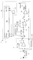
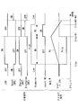
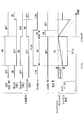
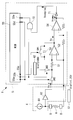
- FIG. 1 is an overall configuration diagram of a biological state quantity measuring device according to a first embodiment of the present invention. It is a timing chart explaining operation
- the biological state quantity measuring device 1 which concerns on the 1st Embodiment of this invention is demonstrated with reference to FIG. 1 and FIG.
- the biological state quantity measuring apparatus 1 is a light emitting diode that irradiates illumination light L to a living body or a biological sample (hereinafter referred to as a living body) A collected from the living body.
- the LED 2 illuminates, for example, blood or body fluid collected from a subject as the living body A or the like with illumination light L. Or you may irradiate the illumination light L directly to the biological sample A which exists in a test subject's body.
- the PD 3 receives, as the signal light L ′, the transmitted light transmitted through the living body A or the like or the reflected light reflected by the living body A or the like.
- the PD 3 outputs a signal current Isig having a magnitude proportional to the light amount of the received signal light L ′.
- the signal light L ′ detected by the PD 3 includes information indicating the state quantity of the living body, such as a glucose level in blood, an oxygen saturation level in blood, and a pulse. Specifically, since the signal light L ′ reflected by the blood is proportional to the glucose concentration and oxygen saturation in the blood, the glucose value and oxygen saturation in the blood are measured from the intensity of the signal light L ′. Can do. Alternatively, since the intensity of the signal light L ′ that has passed through the fingertip changes in synchronization with the contraction and expansion of the blood vessel in the fingertip, the heart rate can be measured from the time change of the signal light L ′.
- the IV conversion circuit 4 includes a current-voltage conversion operational amplifier (hereinafter referred to as an IV operational amplifier) 41 and a conversion resistor connected between an output terminal of the IV operational amplifier 41 and an inverting input terminal (hereinafter referred to as a -input terminal). 42.
- the signal current Isig from the PD 3 flows into the conversion resistor 42.
- the IV operational amplifier 41 is used with a single power source, and a first reference voltage Vref1 generated by a first reference voltage circuit 61 is applied to a non-inverting input terminal (hereinafter referred to as a + input terminal).
- the first reference voltage Vref1 is 1.25V.
- Riv is the resistance value of the conversion resistor 42.
- the AD conversion circuit 5 includes an integration resistor 51, an integration operational amplifier 52, an integration capacitor 53, a comparator 54, and an MCU (micro control unit) 55.
- the integration resistor 51 is connected to the output terminal of the IV operational amplifier 41 via the switch SW2, and the signal voltage Vsig from the IV conversion circuit 4 is input thereto.
- the integrating operational amplifier 52 is applied with the first reference voltage Vref1 to the + input terminal.
- the integrating capacitor 53 is connected between the negative input terminal and the output terminal of the integrating operational amplifier 52.
- the integration capacitor 53 turns on the switch SW1 so that the charging voltage Vc in the initial state becomes the first reference voltage Vref1.
- the switch SW1 and the switch SW3 are turned off and the switch SW2 is turned on and the signal voltage Vsig is input from the IV conversion circuit 4, the difference voltage between the signal voltage Vsig and the first reference voltage Vref1 is obtained.
- the integration capacitor 53 is charged by the integration operational amplifier 52 to generate a charging voltage Vc.
- the integrating capacitor 53 discharges the charged charging voltage Vc to the second reference voltage circuit 62 by turning on the switch SW3 when the switches SW1 and SW2 are off after charging.
- the second reference voltage Vref2 generated by the second reference voltage circuit 62 is set to 3.0V.
- the integration capacitor 53 resets the charging voltage Vc to the first reference voltage Vref1 by turning on the switch SW1.
- the first reference voltage Vref1 is applied to the + input terminal in the same manner as the IV operational amplifier 41.
- the output voltage Vcomp from the comparator 54 is output when the integration voltage Vc greater than the first reference voltage Vref1 is output from the integration operational amplifier 52, that is, during the charging of the integration capacitor 53 and the discharge of the integration capacitor 53. After that, the charge voltage Vc is Low until the voltage drops to the first reference voltage Vref1, and otherwise it is High.
- a NOT circuit 71 is provided after the comparator 54.
- a low digital signal is output from the NOT circuit 71.
- a high digital signal is output from the NOT circuit 71 when the output voltage Vcomp from the comparator 54 is Low.
- the output of the NOT circuit 71 is Vcompinv.
- the MCU 55 incorporates a CPU (Central Processing Unit), a storage device, a timer, and a counter (not shown), and has an input unit and an output unit.
- the MCU stores a program in which processing procedures are recorded in a storage device.
- the CPU reads and executes the program, the output of a signal from the output unit, the measurement of time by a counter, and the signal input to the input unit.
- the control and processing described later, such as the above calculation, are performed.
- the output unit has a charge output terminal (charge) 55a, a discharge output terminal (dicharge) 55b, and a reset output terminal (reset) 55c.
- the input unit has a charging time input terminal (countN1) 55d and a discharging time input terminal (countN2) 55e.
- the charge output terminal 55a outputs an ON command signal for turning on the switch SW2, the discharge output terminal 55b for the switch SW3, and the reset output terminal 55c for the switch SW1.
- the charging output terminal 55a outputs an on command signal and simultaneously outputs a charging time measurement command signal for causing the charging time input terminal 55d to measure the charging time of the integrating capacitor 53.
- the counter measures the charging time count number N1 of the integration capacitor 53 by counting the number of clock signals output from the clock at a constant period.
- a predetermined value for the charging time of the integrating capacitor 53 is set in the MCU 55 in advance.
- the charging time count number N1 when the integrating capacitor 53 is actually charged is counted and used for calculation, so that the charging time is more accurate. The state quantity can be measured.
- the discharge input terminal 55b outputs a discharge time measurement command signal for causing the discharge time input terminal 55e to measure the discharge time count number N2 at the same time as outputting an ON command signal.
- the output discharge time measurement command signal is input to the discharge time input terminal 55e when the output voltage Vcompinv from the NOT circuit 71 is High by the AND circuit 72 provided in the preceding stage of the discharge time input terminal 55e.
- the counter measures the discharge time count number N2 from when the discharge of the integration capacitor 53 is started until the charge voltage Vc drops to the first reference voltage Vref1.
- the MCU 55 calculates the signal voltage Vsig of the IV conversion circuit 4 from the charging time count number N1 and the discharging time count number N2 measured by the counter according to the following equation (1).
- Vsig (Vref2 ⁇ Vref1) ⁇ N2 / N1 (1)
- the MCU 55 calculates the signal current Isig of the PD 3 from the calculated signal voltage Vsig by the following equation (2).
- Isig Vsig / Riv (2)
- the MCU 55 calculates the state quantity of the living body from the signal current Isig obtained from the equation (2) based on the function of the value of the signal current Isig of the PD 3 stored in the storage device and the state quantity of the living body, for example.
- the calculated state quantity is displayed on a display device (not shown).
- Equation (1) is derived as follows. At the time of charging the integrating capacitor 53, the charging voltage Vc, the applied voltage Vsig, and the charging time count number N1 are in the relationship of the following expression (3).
- Rint is a resistance value of the integrating resistor 51
- Cint is a capacitance value of the integrating capacitor 53
- T is a clock cycle.
- Expression (1) is derived.
- the switch SW1 is in the on state and the integrating capacitor 53 in a state where the LED 2 is not emitting light, that is, when the biological state quantity is not measured (t ⁇ t0).
- the charging voltage Vc is reset.
- the ratio of the charging time count number N1 and the discharging time count number N2 is directly proportional to the signal voltage Vsig from the IV conversion circuit 4, that is, the light amount of the signal light L 'from the living body A detected by the PD3. Therefore, the biological state quantity measuring device 1 can calculate the biological state quantity from the measured charging time count number N1, the discharging time count number N2, and the known characteristic values of the respective circuit elements. Further, by integrating the signal voltage Vsig over time, noise included in the signal voltage Vsig is smoothed, and measurement errors due to noise can be removed.
- the calculated value of the signal current Isig of the PD 3 is equal to the resistance value Rint of the integration resistor 51 and the integration capacitor 53. It does not depend on the capacitance value Cint.
- the signal voltage Vsig is charged and discharged by using a common integration capacitor 53 and integration resistor 51. Therefore, even if the resistance value Rint and the capacitance value Cint change, charging and discharging are performed with the same time constant, and therefore the value of the ratio of the charging time count number N1 and the discharging time count number N2 with respect to the signal voltage Vsig. This is because it is uniquely determined. Thereby, even if the characteristic values of the integrating resistor 51 and the integrating capacitor 53 change with time depending on the usage time, the environment of the outside, etc., there is an advantage that an accurate measured value of the state quantity can always be obtained.
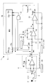
- the biological state quantity measuring apparatus 1 is the first implementation in that different reference voltages Vref1 and Vref3 are applied to the integrating operational amplifier 52 and the IV operational amplifier 41. Different from form.
- the first reference voltage Vref1 is applied to the + input terminal, as in the first embodiment.
- the third reference voltage Vref3 represented by the following expression (5) is applied to the + input terminal.
- Vref3 Vref1 + Riv ⁇ Ioff (5)
- Ioff is an output current (hereinafter referred to as an offset current Ioff) from the PD3 generated by the direct light Ldir that is directly incident on the PD3 without a part of the illumination light L from the LED2 being irradiated on the living body A or the like. It is. That is, when the PD 3 detects the direct light Ldir from the LED 2 due to the arrangement of the PD 3 and the LED 2 or the like, a certain amount of offset current Ioff is output from the PD 3 even under the condition that the living body A or the like does not exist. At this time, as shown in FIG.
- the total output current Isum of the PD 3 is the sum of the signal current Isig resulting from the signal light L ′ to be measured from the living body A or the like and the offset current Ioff.
- the value of the offset current Ioff for example, the output current value of the PD 3 measured when the LED 2 is caused to emit light under the condition that there is no illumination target A such as a living body can be used.
- the discharge time count number N2 of the integration capacitor 53 is set to an amount corresponding to the signal voltage Vsig necessary for the measurement of the state quantity, and an increase in power consumption can be prevented.
- connection between the PD 3 and the IV operational amplifier 41 may be reversed so that the signal current Isig is drawn from the conversion resistor 42.
- the signal voltage Vsig from the IV conversion circuit 4 is positive with respect to the reference voltages Vref1 and Vref3.
- the IV operational amplifier 41 is used with a single power supply and the reference voltages Vref1 and Vref3 are applied. Instead, the reference voltage Vref1 is used with both power supplies. Either Vref1 or Vref3 may be set to zero.
- an excitation light source that illuminates the excitation light of the fluorescent substance is provided in place of the LED 2, and the fluorescence from the fluorescent substance previously supported on the living body A or the like is detected by the PD 3. Good.
- the biomolecule concentration in the biological sample can be measured as the state quantity of the living body by prelabeling the biomolecule in the biological sample with the fluorescent substance.
- the LED 2 and the PD 3 are used as the detection unit, but two or more electrodes may be used instead.
- a pair of positive and negative electrodes 8 are arranged in contact with a living body A or the like, and a constant current is passed between the electrodes 8 by a constant current circuit 81.
- a buffer 82 having a low input impedance receives the potential between the electrodes 8 generated at this time.
- the electric potential generated between the electrodes 8 varies depending on the impedance of the living body A or the like.
- the output from the buffer 82 is input to the AD conversion circuit 5 as the output voltage Vsig. By doing in this way, impedance can be measured as a state quantity of a living body.
- the state quantities of the living body include amino acid concentration, gastrointestinal hormone concentration, other hormone concentration, blood pH, blood glucose concentration, interstitial fluid glucose concentration, and the like. Can be measured.
Landscapes
- Health & Medical Sciences (AREA)
- Life Sciences & Earth Sciences (AREA)
- Physics & Mathematics (AREA)
- Engineering & Computer Science (AREA)
- Heart & Thoracic Surgery (AREA)
- Surgery (AREA)
- Veterinary Medicine (AREA)
- Biophysics (AREA)
- Pathology (AREA)
- Biomedical Technology (AREA)
- Public Health (AREA)
- Medical Informatics (AREA)
- Molecular Biology (AREA)
- Optics & Photonics (AREA)
- Animal Behavior & Ethology (AREA)
- General Health & Medical Sciences (AREA)
- Emergency Medicine (AREA)
- Spectroscopy & Molecular Physics (AREA)
- Theoretical Computer Science (AREA)
- Measurement Of The Respiration, Hearing Ability, Form, And Blood Characteristics Of Living Organisms (AREA)
- Investigating, Analyzing Materials By Fluorescence Or Luminescence (AREA)
- Investigating Or Analysing Materials By Optical Means (AREA)
- Investigating Or Analysing Biological Materials (AREA)
Abstract
回路素子の特性値の経時的な変動によらずに常に正確な測定値を得る。生体または該生体から採取された生体試料(A)から、生体の状態を示す情報を検出するとともに検出した情報を電流として出力する検出部(2,3)と、該検出部(2,3)から出力される電流を電圧に変換する電流電圧変換回路(4)と、該電流電圧変換回路(4)から出力される電圧(Vsig)に基づいて充電された後放電される積分キャパシタ(53)と、該積分キャパシタ(53)の充電時間および放電時間を計測するカウンタ(55)とを有し、該カウンタ(55)により計測された充電時間および放電時間をデジタル量に変換して出力する2重積分型のAD変換回路(5)と、該AD変換回路(5)から出力されたデジタル量に基づいて生体の状態量を算出する情報処理部(55)とを備える生体状態量測定装置(1)を提供する。
Description
本発明は、生体状態量測定装置に関するものである。
従来、生体内にインシュリンを注入する装置において、生体内のグルコースレベルを測定し、得られた測定値に応じてインシュリンの注入量を制御するものが知られている(例えば、特許文献1参照)。測定されたグルコースレベルのアナログ信号は、積分回路を備えたAD変換器によってデジタル信号に変換されてから処理される。
しかしながら、積分回路を構成するキャパシタや抵抗などの回路素子は、使用時間や環境などによって静電容量や抵抗値などの特性値が経時的に変化する。このときに、特許文献1の場合、積分回路の出力が回路素子の特性値の変化とともに変動してしまい、正確な測定値を得ることが難しいという問題がある。
本発明は、上述した事情に鑑みてなされたものであって、回路素子の特性値の経時的な変動によらずに常に正確な測定値を得ることができる生体状態量測定装置を提供することを目的とする。
上記目的を達成するため、本発明は以下の手段を提供する。
本発明は、生体または該生体から採取された生体試料から、前記生体の状態を示す情報を検出するとともに検出した情報を電流として出力する検出部と、該検出部から出力される電流を電圧に変換する電流電圧変換回路と、該電流電圧変換回路から出力される電圧に基づいて充電された後放電される積分キャパシタと、該積分キャパシタの充電時間および放電時間を計測するカウンタとを有し、該カウンタにより計測された充電時間および放電時間をデジタル量に変換して出力する2重積分型のAD変換回路と、該AD変換回路から出力されたデジタル量に基づいて前記生体の状態量を算出する情報処理部とを備える生体状態量測定装置を提供する。
本発明は、生体または該生体から採取された生体試料から、前記生体の状態を示す情報を検出するとともに検出した情報を電流として出力する検出部と、該検出部から出力される電流を電圧に変換する電流電圧変換回路と、該電流電圧変換回路から出力される電圧に基づいて充電された後放電される積分キャパシタと、該積分キャパシタの充電時間および放電時間を計測するカウンタとを有し、該カウンタにより計測された充電時間および放電時間をデジタル量に変換して出力する2重積分型のAD変換回路と、該AD変換回路から出力されたデジタル量に基づいて前記生体の状態量を算出する情報処理部とを備える生体状態量測定装置を提供する。
本発明によれば、検出部によって出力された電流は、電流電圧変換回路(IV変換回路)によって電圧に変換され、電流変換回路から出力される電圧に基づいて積分キャパシタが充電された後放電される。ここで、積分キャパシタの充電時間に対する放電時間の比は、IV変換回路からの出力電圧、すなわち、検出部から出力される電流に依存する。したがって、情報処理部は、カウンタによって計測された充電時間および放電時間のデジタル量から生体の状態量を算出することができる。
この場合に、2重積分型のAD変換回路においては積分キャパシタの充電および放電は共通の経路を介して行われるので、その経路内の回路素子の特性値が変化しても、電流電圧変換回路からの出力電圧が同一であれば、充電時間に対する放電時間の比は一定になる。すなわち、回路素子の特性値が経時的に変化してもその変化に依らずに、常に安定した状態量の測定値を得ることができる。
第1の態様に係る生体状態量測定装置は、前記電流電圧変換回路が第1の基準電圧に基づいて前記検出部から出力される電流を電圧に変換し、前記2重積分型のAD変換回路が前記第1の基準電圧とは異なる第2の基準電圧に基づいて前記積分キャパシタを放電させる。
第2の態様に係る生体状態量測定装置は、前記AD変換回路が第1の基準電圧に基づいて動作し、前記電流電圧変換回路が前記第1の基準電圧とは異なる第3の基準電圧に基づいて前記検出部から出力される電流を電圧に変換し、前記電流電圧変換回路が前記第3の基準電圧に対して負の電圧を出力する場合は、前記第3の基準電圧が前記第1の基準電圧より高く設定され、前記電流電圧変換回路が前記第3の基準電圧に対して正の電圧を出力する場合は、前記第3の基準電圧が前記第1の基準電圧より低く設定されている。
このようにすることで、検出部から出力される電流に、生体からの情報に起因した電流以外のオフセット電流が含まれる場合に、該オフセット電流によるIV変換回路の出力電圧の絶対値の増加が抑えられる。その結果、積分キャパシタの放電時間が短縮されるので、カウンタによる放電時間の計測時間が短縮され、消費電力の増加を抑えることができる。
また、本発明の第3の態様に係る生体状態量測定装置は、前記検出部が、前記生体または前記生体試料に照明光を照射する照明光源と、前記生体または前記生体試料により反射された前記照明光の反射光、もしくは、前記生体または前記生体試料を透過した前記照明光の透過光を受光して電流として出力するフォトダイオードとを備える。
このようにすることで、反射光または透過光の強度に基づいて、生体または生体試料に含まれる生体分子の濃度などの状態量を測定することができる。
このようにすることで、反射光または透過光の強度に基づいて、生体または生体試料に含まれる生体分子の濃度などの状態量を測定することができる。
また、本発明の第4の態様に係る生体状態量測定装置は、前記検出部が、前記生体または前記生体試料に接触させられ、前記生体または前記生体試料を流れる電流を検出する少なくとも2つの電極を備える。
このようにすることで、生体または生体試料を流れる電流の大きさやその変化に基づいて、心拍などの状態量を測定することができる。
このようにすることで、生体または生体試料を流れる電流の大きさやその変化に基づいて、心拍などの状態量を測定することができる。
また、本発明の第5の態様に係る生体状態量測定装置は、前記検出部が、前記生体または前記生体試料に、該生体または生体試料に担持させられた蛍光物質を励起する励起光を照明する励起光源と、前記蛍光物質からの蛍光を受光して電流として出力するフォトダイオードとを備える。
このようにすることで、蛍光強度に基づいて、生体または生体試料に含まれる生体分子の濃度などの状態量を測定することができる。
このようにすることで、蛍光強度に基づいて、生体または生体試料に含まれる生体分子の濃度などの状態量を測定することができる。
本発明によれば、回路素子の特性値の経時的な変動によらずに常に正確な測定値を得ることができるという効果を奏する。
(第1の実施形態)
以下に、本発明の第1の実施形態に係る生体状態量測定装置1について、図1および図2を参照して説明する。
本実施形態に係る生体状態量測定装置1は、図1に示されるように、生体または該生体から採取された生体試料(以下、生体等という。)Aに照明光Lを照射する発光ダイオード(LED、検出部、照明光源)2と、生体等Aからの信号光L’を検出するフォトダイオード(PD、検出部)3と、該PD3からの信号電流Isigを信号電圧Vsigに変換する電流電圧変換回路(IV変換回路)4と、該IV変換回路4からの信号電圧Vsigに基づいて生体の状態量を算出する2重積分型のAD変換回路5とを備えている。
以下に、本発明の第1の実施形態に係る生体状態量測定装置1について、図1および図2を参照して説明する。
本実施形態に係る生体状態量測定装置1は、図1に示されるように、生体または該生体から採取された生体試料(以下、生体等という。)Aに照明光Lを照射する発光ダイオード(LED、検出部、照明光源)2と、生体等Aからの信号光L’を検出するフォトダイオード(PD、検出部)3と、該PD3からの信号電流Isigを信号電圧Vsigに変換する電流電圧変換回路(IV変換回路)4と、該IV変換回路4からの信号電圧Vsigに基づいて生体の状態量を算出する2重積分型のAD変換回路5とを備えている。
LED2は、生体等Aとして、例えば、被験者から採取した血液や体液に照明光Lを照射する。あるいは、被験者の体内に存在する生体試料Aに直接照明光Lを照射してもよい。
PD3は、照明光Lが生体等Aを透過した透過光または生体等Aで反射された反射光を信号光L’として受光する。PD3は、受光した信号光L’の光量に比例した大きさの信号電流Isigを出力する。
PD3は、照明光Lが生体等Aを透過した透過光または生体等Aで反射された反射光を信号光L’として受光する。PD3は、受光した信号光L’の光量に比例した大きさの信号電流Isigを出力する。
PD3によって検出される信号光L’は、例えば、血液中のグルコース値、血液中の酸素飽和度、脈拍などの生体の状態量を示す情報を含んでいる。具体的には、血液で反射された信号光L’は、血液中のグルコース濃度や酸素飽和度に比例するので、信号光L’の強度から血液中のグルコース値や酸素飽和度を測定することができる。あるいは、指先を透過してきた信号光L’の強度は指先内の血管の収縮及び拡張と同期して変化するので、信号光L’の時間変化から心拍数を測定することができる。
IV変換回路4は、電流電圧変換オペアンプ(以下、IVオペアンプという。)41と、該IVオペアンプ41の出力端子と反転入力端子(以下、-入力端子という。)との間に接続された変換抵抗42とを備えている。PD3からの信号電流Isigは、変換抵抗42に流れ込む。IVオペアンプ41は、単電源で使用され、第1の基準電圧回路61により生成された第1の基準電圧Vref1が非反転入力端子(以下、+入力端子という。)に印加されている。本実施形態においては、第1の基準電圧Vref1を1.25Vとする。IV変換回路4は、PD3からの信号電流Isigが入力されたときに、信号電圧Vsig=1.25V-Isig×Rivを出力する。ここで、Rivは変換抵抗42の抵抗値である。
AD変換回路5は、積分抵抗51と、積分オペアンプ52と、積分キャパシタ53と、コンパレータ54と、MCU(マイクロコントロールユニット)55とを備えている。
積分抵抗51は、スイッチSW2を介してIVオペアンプ41の出力端子と接続され、IV変換回路4からの信号電圧Vsigが入力される。
積分オペアンプ52は、IVオペアンプ41と同様に、第1の基準電圧Vref1が+入力端子に印加さている。
積分抵抗51は、スイッチSW2を介してIVオペアンプ41の出力端子と接続され、IV変換回路4からの信号電圧Vsigが入力される。
積分オペアンプ52は、IVオペアンプ41と同様に、第1の基準電圧Vref1が+入力端子に印加さている。
積分キャパシタ53は、積分オペアンプ52の-入力端子と出力端子との間に接続されている。積分キャパシタ53は、スイッチSW1をオン状態にすることで、初期状態における充電電圧Vcが第1の基準電圧Vref1になる。次に、スイッチSW1,SW3のオフ状態において、スイッチSW2がオン状態になってIV変換回路4から信号電圧Vsigが入力されたときに、信号電圧Vsigと第1の基準電圧Vref1との差分電圧により、積分キャパシタ53は積分オペアンプ52により充電され、充電電圧Vcが生成される。
次に、積分キャパシタ53は、充電後にスイッチSW1,SW2がオフ状態においてスイッチSW3がオン状態にされることにより、充電した充電電圧Vcを第2の基準電圧回路62に放電する。本実施形態においては、第2の基準電圧回路62が生成する第2の基準電圧Vref2を3.0Vとする。その後、積分キャパシタ53は、スイッチSW1がオン状態にされることにより、充電電圧Vcを第1の基準電圧Vref1にリセットする。
コンパレータ54は、IVオペアンプ41と同様に、+入力端子に第1の基準電圧Vref1が印加されている。これにより、コンパレータ54からの出力電圧Vcompは、積分オペアンプ52から第1の基準電圧Vref1より大きい積分電圧Vcが出力されているとき、すなわち、積分キャパシタ53の充電中および積分キャパシタ53の放電が開始されてからその充電電圧Vcが第1の基準電圧Vref1まで降下するまでの間はLowとなり、それ以外のときはHighとなる。
コンパレータ54の後段には、NOT回路71が設けられている。コンパレータ54の出力電圧VcompがHighのときにはNOT回路71からLowのデジタル信号が出力される。一方、コンパレータ54からの出力電圧VcompがLowのときにはNOT回路71からHighのデジタル信号が出力される。NOT回路71の出力をVcompinvとする。
MCU55は、図示しないCPU(中央処理装置)、記憶装置、タイマおよびカウンタを内蔵し、また、入力部および出力部を有している。MCUは、処理手順を記録したプログラムが記憶装置に記憶されており、プログラムをCPUが読み出して実行することにより、出力部からの信号の出力、カウンタによる時間の計測、入力部に入力された信号の演算などの後述する制御や処理を行う。
出力部は、充電出力端子(charge)55a、放電出力端子(dicharge)55bおよびリセット出力端子(reset)55cを有している。入力部は、充電時間入力端子(countN1)55dおよび放電時間入力端子(countN2)55eを有している。充電出力端子55aはスイッチSW2に、放電出力端子55bはスイッチSW3に、リセット出力端子55cはスイッチSW1に対して、オン状態にするオン指令信号を出力する。
また、充電出力端子55aは、オン指令信号を出力すると同時に、充電時間入力端子55dに積分キャパシタ53の充電時間を計測させる充電時間計測指令信号を出力する。これにより、カウンタは、クロックから一定周期で出力されるクロック信号の数をカウントすることにより、積分キャパシタ53の充電時間カウント数N1を計測するようになっている。ここで、積分キャパシタ53の充電時間は所定の値がMCU55に予め設定されているが、積分キャパシタ53が実際に充電された充電時間カウント数N1をカウントして演算に用いることにより、さらに正確に状態量を測定することができる。
放電用入力端子55bは、オン指令信号を出力すると同時に、放電時間入力端子55eに放電時間カウント数N2を計測させる放電時間計測指令信号を出力する。出力された放電時間計測指令信号は、放電時間入力端子55eの前段に設けられたAND回路72により、NOT回路71からの出力電圧VcompinvがHighであれば、放電時間入力端子55eに入力される。これにより、カウンタは、積分キャパシタ53の放電が開始されてからその充電電圧Vcが第1の基準電圧Vref1まで降下するまでの放電時間カウント数N2を計測するようになっている。
MCU55は、カウンタが計測した充電時間カウント数N1と放電時間カウント数N2とから、下式(1)により、IV変換回路4の信号電圧Vsigを算出する。
Vsig = (Vref2 - Vref1) × N2/N1 ・・・(1)
さらに、MCU55は、算出した信号電圧Vsigから、下式(2)により、PD3の信号電流Isigを算出する。
Isig = Vsig/Riv ・・・(2)
Vsig = (Vref2 - Vref1) × N2/N1 ・・・(1)
さらに、MCU55は、算出した信号電圧Vsigから、下式(2)により、PD3の信号電流Isigを算出する。
Isig = Vsig/Riv ・・・(2)
MCU55は、例えば、記憶装置に記憶されたPD3の信号電流Isigの値と生体の状態量との関数に基づいて、式(2)より得られた信号電流Isigから生体の状態量を算出し、算出した状態量を図示しない表示装置などに表示させる。
なお、式(1)は、以下のようにして導出される。
積分キャパシタ53の充電時において、充電電圧Vc、印加電圧Vsig、充電時間カウント数N1は下式(3)の関係にある。ここで、Rintは積分抵抗51の抵抗値、Cintは積分キャパシタ53の静電容量値、Tはクロックの周期である。
積分キャパシタ53の充電時において、充電電圧Vc、印加電圧Vsig、充電時間カウント数N1は下式(3)の関係にある。ここで、Rintは積分抵抗51の抵抗値、Cintは積分キャパシタ53の静電容量値、Tはクロックの周期である。

一方、積分キャパシタ53の放電時において、充電電圧Vc、印加電圧Vref2-Vref1、放電時間カウント数N2は下式(4)の関係にある。
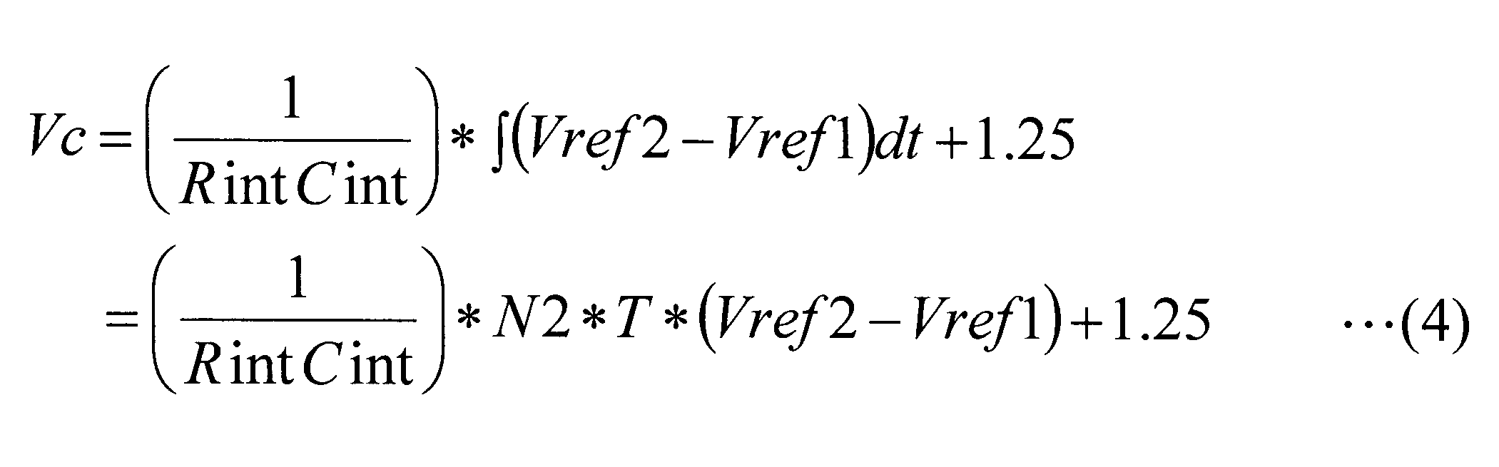
ここで、式(3)と式(4)の左辺は等しいことから、式(1)が導出される。
このように構成された生体状態量測定装置1の動作および作用について、図2のタイミングチャートを参照して以下に説明する。
本実施形態に係る生体状態量測定装置1は、LED2が発光していない、すなわち、生体の状態量を測定していない状態(t<t0)においては、スイッチSW1がオン状態であり積分キャパシタ53の充電電圧Vcがリセットされている。
本実施形態に係る生体状態量測定装置1は、LED2が発光していない、すなわち、生体の状態量を測定していない状態(t<t0)においては、スイッチSW1がオン状態であり積分キャパシタ53の充電電圧Vcがリセットされている。
生体状態量測定装置1は、LED2を発光させたときに(t=t0)、スイッチSW1をオフ状態にし、スイッチSW2をオン状態し、PD3からの信号電圧Vsigを充電時間カウント数N1にわたって積分キャパシタ53で積分し、充電時間カウント数N1を計測する(t0≦t≦t0+N1)。生体状態量測定装置1は、信号電圧Vsigを積分した後(t=t0+N1)、スイッチSW3をオン状態にして積分キャパシタ53から放電し、積分した信号電圧Vsigの放電時間カウント数N2を計測する(t0+N1≦t≦t0+N1+N2)。
充電時間カウント数N1と放電時間カウント数N2の比は、IV変換回路4からの信号電圧Vsig、すなわち、PD3によって検出された生体等Aから信号光L’の光量に正比例する。したがって、生体状態量測定装置1は、測定した充電時間カウント数N1と放電時間カウント数N2と既知の各回路素子の特性値とから、生体の状態量を算出することができる。また、信号電圧Vsigを時間で積分することにより、信号電圧Vsigに含まれるノイズが平滑化され、ノイズに由来する測定誤差を除去することができる。
この場合に、本実施形態によれば、式(1)および式(2)で示されるように、算出されるPD3の信号電流Isigの値は、積分抵抗51の抵抗値Rintおよび積分キャパシタ53の静電容量値Cintに依存しない。これは、2重積分型のAD変換回路5においては、共通の積分キャパシタ53および積分抵抗51を用いて信号電圧Vsigを充電および放電している。したがって、抵抗値Rintや静電容量値Cintが変化しても、同一の時定数で充電および放電されるので、信号電圧Vsigに対して充電時間カウント数N1と放電時間カウント数N2の比の値は一意に決まるためである。これにより、使用時間や外界の環境などによって積分抵抗51や積分キャパシタ53の特性値が経時的に変化しても、常に正確な状態量の測定値を得ることができるという利点がある。
(第2の実施形態)
次に、本発明の第2の実施形態に係る生体状態量測定装置1について、図3~図6を参照して以下に説明する。
なお、本実施形態においては、上述した第1の実施形態と異なる点について主に説明し、第1の実施形態と共通する構成については同一の符号を付して説明を省略する。
次に、本発明の第2の実施形態に係る生体状態量測定装置1について、図3~図6を参照して以下に説明する。
なお、本実施形態においては、上述した第1の実施形態と異なる点について主に説明し、第1の実施形態と共通する構成については同一の符号を付して説明を省略する。
本実施形態に係る生体状態量測定装置1は、図3に示されるように、積分オペアンプ52とIVオペアンプ41とに、互いに異なる基準電圧Vref1,Vref3が印加されている点において、第1の実施形態と異なる。
積分オペアンプ53は、第1の実施形態と同様に、+入力端子に第1の基準電圧Vref1が印加されている。
IVオペアンプ41は、+入力端子に下式(5)で表される第3の基準電圧Vref3が印加されている。
Vref3 =Vref1 + Riv×Ioff・・・(5)
IVオペアンプ41は、+入力端子に下式(5)で表される第3の基準電圧Vref3が印加されている。
Vref3 =Vref1 + Riv×Ioff・・・(5)
ここで、Ioffは、LED2からの照明光Lの一部が、生体等Aに照射されずにPD3に直接入射した直接光Ldirによって発生するPD3からの出力電流(以下、オフセット電流Ioffという。)である。すなわち、PD3およびLED2の配置などによってPD3がLED2からの直接光Ldirを検出してしまう状況にある場合、生体等Aが存在しない条件でもPD3から一定量のオフセット電流Ioffが出力されてしまう。このときに、図4に示されるように、PD3の全出力電流Isumは、生体等Aからの測定すべき信号光L’に起因する信号電流Isigと、オフセット電流Ioffとの和になる。オフセット電流Ioffの値は、例えば、生体等Aの照明対象がない条件でLED2を発光させたときに測定されたPD3の出力電流値を用いることができる。
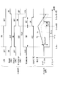
第1の実施形態に係る生体状態量測定装置1の構成においてPD3にオフセット電流Ioffが存在する場合、図5に破線で示されるように、生体等Aを測定していない状態でもLED2が点灯していればIV変換回路4から出力されるオフセット電圧Voff=Riv×Ioffにより積分キャパシタ53の充電電圧Vcが上昇する。その結果、生体等Aを測定したときに、図5に実線で示されるように、積分キャパシタ52の放電時間カウント数N2が、オフセット電圧Voffによる充電電圧Vcの上昇分(図5のtoff)だけ増大する。
このように、放電時間カウント数N2の計測時間が長くなることにより、消費電力が不要に大きくなってしまうという問題がある。また、オフセット電圧Voffを考慮して積分キャパシタ52および積分抵抗51として特性値Cint,Rintの大きなものを選択しなければならないため、ノイズが増大したり回路素子51,52の寸法が大きくなって装置1全体が大きくなるなどの問題がある。
これに対し、本実施形態に係る生体状態量測定装置1の構成によれば、IVオペアンプ41に第3の基準電圧Vref3を印加することにより、図6に示されるように、IV変換回路4からはオフセット電圧Voffが除去された電圧が出力される。これにより、積分キャパシタ53の放電時間カウント数N2を、状態量の測定に必要な信号電圧Vsigに相当する分だけにし、消費電力の増大を防ぐことができるという利点がある。
(他の実施形態)
上述した第1および第2の実施形態においては、PD3とIVオペアンプ41との接続を逆にして、信号電流Isigを変換抵抗42から引き込む向きにしてもよい。この場合、IV変換回路4からの信号電圧Vsigは、基準電圧Vref1,Vref3に対して正になる。また、第2の実施形態において、基準電圧Vref3は、
Vref3 = Vref1-Riv*Ioff・・・(5)’
となる。
上述した第1および第2の実施形態においては、PD3とIVオペアンプ41との接続を逆にして、信号電流Isigを変換抵抗42から引き込む向きにしてもよい。この場合、IV変換回路4からの信号電圧Vsigは、基準電圧Vref1,Vref3に対して正になる。また、第2の実施形態において、基準電圧Vref3は、
Vref3 = Vref1-Riv*Ioff・・・(5)’
となる。
また、第1および第2の実施形態においては、IVオペアンプ41を単電源で使用して基準電圧Vref1,Vref3を印加することとしたが、これに代えて、両電源で使用して、基準電圧Vref1,Vref3のいずれかをゼロにしてもよい。
また、第1および第2の実施形態においては、LED2に代えて蛍光物質の励起光を照明する励起光源を備え、生体等Aに予め担持させた蛍光物質からの蛍光をPD3で検出してもよい。
このようにすることで、例えば、生体試料中の生体分子を蛍光物質により予め標識しておくことにより、生体の状態量として生体分子の濃度を測定することができる。
このようにすることで、例えば、生体試料中の生体分子を蛍光物質により予め標識しておくことにより、生体の状態量として生体分子の濃度を測定することができる。
また、第1および第2の実施形態においては、検出部としてLED2およびPD3を用いることとしたが、これに代えて、2つ以上の電極を用いてもよい。例えば、図7に示されるように、正負の一対の電極8を生体等Aに接触状態に配置し、電極8間に定電流回路81により一定電流を流す。このときに発生した電極8間の電位を入力インピーダンスの低いバッファ82が受ける。ここで、電極8間で発生する電位は、生体等Aのインピーダンスにより変化する。バッファ82からの出力は出力電圧VsigとしてAD変換回路5に入力される。
このようにすることで、生体の状態量としてインピーダンスを測定することができる。
このようにすることで、生体の状態量としてインピーダンスを測定することができる。
また、第1および第2の実施形態においては、生体の状態量として、アミノ酸濃度、胃腸ホルモン濃度、他のホルモン濃度、血液のpH、血液中のグルコース濃度、組織間液中のグルコース濃度なども測定することができる。
1 生体状態量測定装置
2 発光ダイオード(検出部、照明光源)
3 フォトダイオード(検出部)
4 電流電圧変換回路
5 AD変換回路
8 電極(検出部)
41 電流電圧変換オペアンプ
42 変換抵抗
51 積分抵抗
52 積分オペアンプ
53 積分キャパシタ
54 コンパレータ
55 マイクロコントロールユニット(カウンタ、情報処理部)
55a~55c 入力端子
55d,55e 出力端子
61,62,63 基準電圧回路
71 NOT回路
72 AND回路
81 定電流回路
82 バッファ
A 生体または生体試料
2 発光ダイオード(検出部、照明光源)
3 フォトダイオード(検出部)
4 電流電圧変換回路
5 AD変換回路
8 電極(検出部)
41 電流電圧変換オペアンプ
42 変換抵抗
51 積分抵抗
52 積分オペアンプ
53 積分キャパシタ
54 コンパレータ
55 マイクロコントロールユニット(カウンタ、情報処理部)
55a~55c 入力端子
55d,55e 出力端子
61,62,63 基準電圧回路
71 NOT回路
72 AND回路
81 定電流回路
82 バッファ
A 生体または生体試料
Claims (6)
- 生体または該生体から採取された生体試料から、前記生体の状態を示す情報を検出するとともに検出した情報を電流として出力する検出部と、
該検出部から出力される電流を電圧に変換する電流電圧変換回路と、
該電流電圧変換回路から出力される電圧に基づいて充電された後放電される積分キャパシタと、該積分キャパシタの充電時間および放電時間を計測するカウンタとを有し、該カウンタにより計測された充電時間および放電時間をデジタル量に変換して出力する2重積分型のAD変換回路と、
該AD変換回路から出力された前記デジタル量に基づいて前記生体の状態量を算出する情報処理部とを備える生体状態量測定装置。 - 前記電流電圧変換回路は、第1の基準電圧に基づいて前記検出部から出力される電流を電圧に変換し、
前記2重積分型のAD変換回路は、前記第1の基準電圧とは異なる第2の基準電圧に基づいて前記積分キャパシタを放電させる請求項1に記載の生体状態量測定装置。 - 前記2重積分型のAD変換回路は、第1の基準電圧に基づいて動作し、
前記電流電圧変換回路は、前記第1の基準電圧とは異なる第3の基準電圧に基づいて前記検出部から出力される電流を電圧に変換し、
前記電流電圧変換回路が前記第3の基準電圧に対して負の電圧を出力する場合は、前記第3の基準電圧が前記第1の基準電圧より高く設定され、
前記電流電圧変換回路が前記第3の基準電圧に対して正の電圧を出力する場合は、前記第3の基準電圧が前記第1の基準電圧より低く設定されている請求項1に記載の生体状態量測定装置。 - 前記検出部が、
前記生体または前記生体試料に照明光を照射する照明光源と、
前記生体または前記生体試料により反射された前記照明光の反射光、もしくは、前記生体または前記生体試料を透過した前記照明光の透過光を受光して電流として出力するフォトダイオードとを備える請求項1~3のいずれか1項に記載の生体状態量測定装置。 - 前記検出部が、
前記生体または前記生体試料に接触させられ、該生体または生体試料を流れる電流を検出する少なくとも2つの電極を備える請求項1~3のいずれか1項に記載の生体状態量測定装置。 - 前記検出部が、
前記生体または前記生体試料に、該生体または生体試料に担持させられた蛍光物質を励起する励起光を照明する励起光源と、
前記蛍光物質からの蛍光を受光して電流として出力するフォトダイオードとを備える請求項1~3のいずれか1項に記載の生体状態量測定装置。
Priority Applications (2)
| Application Number | Priority Date | Filing Date | Title |
|---|---|---|---|
| CN201180034480.8A CN103096792B (zh) | 2010-07-16 | 2011-03-11 | 生物体状态量测定装置 |
| US13/736,359 US9041582B2 (en) | 2010-07-16 | 2013-01-08 | Organism state quantity measuring apparatus |
Applications Claiming Priority (2)
| Application Number | Priority Date | Filing Date | Title |
|---|---|---|---|
| JP2010-161812 | 2010-07-16 | ||
| JP2010161812A JP5701528B2 (ja) | 2010-07-16 | 2010-07-16 | 生体状態量測定装置 |
Related Child Applications (1)
| Application Number | Title | Priority Date | Filing Date |
|---|---|---|---|
| US13/736,359 Continuation US9041582B2 (en) | 2010-07-16 | 2013-01-08 | Organism state quantity measuring apparatus |
Publications (1)
| Publication Number | Publication Date |
|---|---|
| WO2012008178A1 true WO2012008178A1 (ja) | 2012-01-19 |
Family
ID=45469192
Family Applications (1)
| Application Number | Title | Priority Date | Filing Date |
|---|---|---|---|
| PCT/JP2011/055793 Ceased WO2012008178A1 (ja) | 2010-07-16 | 2011-03-11 | 生体状態量測定装置 |
Country Status (4)
| Country | Link |
|---|---|
| US (1) | US9041582B2 (ja) |
| JP (1) | JP5701528B2 (ja) |
| CN (1) | CN103096792B (ja) |
| WO (1) | WO2012008178A1 (ja) |
Families Citing this family (9)
| Publication number | Priority date | Publication date | Assignee | Title |
|---|---|---|---|---|
| WO2014062985A1 (en) | 2012-10-17 | 2014-04-24 | University Of Maryland, Office Of Technology Commercialization | Device and methods of using device for detection of aminoacidopathies |
| JP6998658B2 (ja) * | 2014-04-17 | 2022-01-18 | ユニバーシティ オブ メリーランド, カレッジ パーク | アミノ酸代謝異常の検出のためのデバイス、及びデバイスを使用する方法 |
| US10499821B2 (en) | 2014-07-23 | 2019-12-10 | Shenzhen GOODIX Technology Co., Ltd. | Optical heart rate sensor |
| US10158372B1 (en) * | 2017-06-20 | 2018-12-18 | Taiwan Semiconductor Manufcturing Company, Ltd. | Analog to digital converter |
| CA3061574C (en) * | 2017-07-03 | 2022-07-26 | F. Hoffmann-La Roche Ag | Method and electronics unit for detecting in-vivo properties of a biosensor |
| WO2019032488A1 (en) * | 2017-08-07 | 2019-02-14 | DePuy Synthes Products, Inc. | IMPLANTABLE SENSORS IN THE BODY OF A PATIENT, SYSTEMS AND METHODS OF USING THE SAME |
| CN109452944B (zh) * | 2017-09-06 | 2023-08-15 | 东北大学 | 基于荧光脉搏波的血液荧光物质无创检测系统 |
| CN109596583A (zh) * | 2018-11-23 | 2019-04-09 | 中国科学院苏州生物医学工程技术研究所 | 生物荧光快速检测装置 |
| GB2630057B (en) * | 2023-05-15 | 2026-04-22 | Glucorx Tech Limited | Current measurement device for an analyte monitoring system |
Citations (4)
| Publication number | Priority date | Publication date | Assignee | Title |
|---|---|---|---|---|
| JP2007222669A (ja) * | 2003-10-28 | 2007-09-06 | Veralight Inc | 組織の蛍光発光を用いた糖化最終産物または疾病状態の尺度の決定 |
| WO2009067626A1 (en) * | 2007-11-21 | 2009-05-28 | Glumetrics, Inc. | Use of an equilibrium intravascular sensor to achieve tight glycemic control |
| JP2009271010A (ja) * | 2008-05-09 | 2009-11-19 | Panasonic Electric Works Co Ltd | センサ装置 |
| JP4487015B1 (ja) * | 2009-12-08 | 2010-06-23 | 株式会社クロスウェル | 自律神経機能評価装置およびプログラム |
Family Cites Families (17)
| Publication number | Priority date | Publication date | Assignee | Title |
|---|---|---|---|---|
| DE3408824A1 (de) * | 1984-03-10 | 1985-09-12 | Vdo Adolf Schindling Ag, 6000 Frankfurt | Schaltungsanordnung zur elektrothermischen, umgebungstemperatur-kompensierten fuellstandsmessung |
| US4909633A (en) * | 1986-05-12 | 1990-03-20 | Minolta Camera Kabushiki Kaisha | Multi-channel spectral light measuring device |
| JPS6365845A (ja) * | 1986-09-05 | 1988-03-24 | ミノルタ株式会社 | オキシメ−タ装置 |
| FR2622375B1 (fr) * | 1987-10-21 | 1990-02-02 | Commissariat Energie Atomique | Convertisseur analogique numerique a grande dynamique |
| DE69111800T2 (de) * | 1991-06-20 | 1995-12-14 | Hewlett Packard Gmbh | Photodiodenanordnung. |
| US5614902A (en) * | 1994-11-30 | 1997-03-25 | Sgs-Thomson Microelectronics, Inc. | Ratiometric analog to digital converter with automatic offset |
| FR2738426B1 (fr) * | 1995-08-29 | 1998-02-13 | Univ Neuchatel | Dispositif de traitement numerique d'un signal analogique devant etre restitue sous forme analogique |
| US6163715A (en) | 1996-07-17 | 2000-12-19 | Criticare Systems, Inc. | Direct to digital oximeter and method for calculating oxygenation levels |
| US6558351B1 (en) | 1999-06-03 | 2003-05-06 | Medtronic Minimed, Inc. | Closed loop system for controlling insulin infusion |
| JP3734350B2 (ja) * | 1997-10-17 | 2006-01-11 | 株式会社タニタ | 体内脂肪量計および体内脂肪量計付き体重計 |
| US6856125B2 (en) * | 2001-12-12 | 2005-02-15 | Lifescan, Inc. | Biosensor apparatus and method with sample type and volume detection |
| CN1806475B (zh) | 2003-04-15 | 2013-07-03 | 医药及科学传感器公司 | 具有集成天线的印刷电路装置和具有集成印刷电路板天线的可植入传感器处理系统 |
| JP4113824B2 (ja) * | 2003-09-24 | 2008-07-09 | シリンクス株式会社 | 光空間通信用受信回路 |
| CN1882278A (zh) * | 2003-10-28 | 2006-12-20 | 薇拉莱特公司 | 使用组织荧光确定某一糖化终产物或疾病状态 |
| JP2006133120A (ja) * | 2004-11-08 | 2006-05-25 | Seiko Epson Corp | 電流積算回路 |
| JP4929060B2 (ja) * | 2006-07-14 | 2012-05-09 | ローム株式会社 | アナログ/ディジタル変換器、照度センサ、照明装置、電子機器 |
| KR100901694B1 (ko) * | 2006-12-08 | 2009-06-08 | 한국전자통신연구원 | 전류모드 이중 적분형 변환장치 |
-
2010
- 2010-07-16 JP JP2010161812A patent/JP5701528B2/ja not_active Expired - Fee Related
-
2011
- 2011-03-11 CN CN201180034480.8A patent/CN103096792B/zh not_active Expired - Fee Related
- 2011-03-11 WO PCT/JP2011/055793 patent/WO2012008178A1/ja not_active Ceased
-
2013
- 2013-01-08 US US13/736,359 patent/US9041582B2/en not_active Expired - Fee Related
Patent Citations (4)
| Publication number | Priority date | Publication date | Assignee | Title |
|---|---|---|---|---|
| JP2007222669A (ja) * | 2003-10-28 | 2007-09-06 | Veralight Inc | 組織の蛍光発光を用いた糖化最終産物または疾病状態の尺度の決定 |
| WO2009067626A1 (en) * | 2007-11-21 | 2009-05-28 | Glumetrics, Inc. | Use of an equilibrium intravascular sensor to achieve tight glycemic control |
| JP2009271010A (ja) * | 2008-05-09 | 2009-11-19 | Panasonic Electric Works Co Ltd | センサ装置 |
| JP4487015B1 (ja) * | 2009-12-08 | 2010-06-23 | 株式会社クロスウェル | 自律神経機能評価装置およびプログラム |
Also Published As
| Publication number | Publication date |
|---|---|
| CN103096792B (zh) | 2015-01-21 |
| JP2012020054A (ja) | 2012-02-02 |
| JP5701528B2 (ja) | 2015-04-15 |
| US20130201049A1 (en) | 2013-08-08 |
| CN103096792A (zh) | 2013-05-08 |
| US9041582B2 (en) | 2015-05-26 |
Similar Documents
| Publication | Publication Date | Title |
|---|---|---|
| JP5701528B2 (ja) | 生体状態量測定装置 | |
| JP4914170B2 (ja) | ブドウ糖濃度を計算するための電流試料を処理するシステム及び方法 | |
| CN103907115B (zh) | 传感器数据的后向校准 | |
| CN102611421A (zh) | 传感器装置以及电子设备 | |
| JP5863791B2 (ja) | 比色センサを有する血液培養ボトル用検出装置 | |
| WO2011033875A1 (ja) | 血糖計 | |
| US20180321181A1 (en) | Oxygen sensor | |
| JP2013205325A (ja) | 電流測定装置 | |
| CN101849189A (zh) | 具有宽动态范围的电流积分器 | |
| JP2008232662A (ja) | 光学測定装置 | |
| US11864876B2 (en) | Light-to-digital converter | |
| Zhi et al. | Lock-in based phase fluorometric dissolved oxygen sensor interface with 4 kHz–150 kHz tunable excitation frequency and frequency error calibration | |
| US11464416B2 (en) | Measurement circuit, driving method, and electronic instrument | |
| JP2013104839A (ja) | 生体情報量検出装置および生体情報量検出方法 | |
| CN205139013U (zh) | 一种可自动调节光强度的荧光物质浓度检测装置 | |
| JPH0559734B2 (ja) | ||
| US20100057376A1 (en) | Optical detecting method and apparatus | |
| US20250130162A1 (en) | Charge-to-digital converter for time-domain dual lifetime referencing | |
| TWI388833B (zh) | 生物感測裝置 | |
| CN1515682A (zh) | 可校正环境温度效应的生物传感器及其方法 | |
| CN109556738A (zh) | 模拟测量方法、测量数据拟合方法及化学发光测定仪 | |
| Wang et al. | Solution ion luminescence induced by the triboelectric-discharge effect for rapid and intuitive detection of sweat ions | |
| RU60222U1 (ru) | Устройство для определения интегральной антиоксидантной емкости биологических сред | |
| KR20170014668A (ko) | 정전용량 변화측정장치 | |
| WO2025090597A1 (en) | Charge-to-digital converter for time-domain dual lifetime referencing |
Legal Events
| Date | Code | Title | Description |
|---|---|---|---|
| WWE | Wipo information: entry into national phase |
Ref document number: 201180034480.8 Country of ref document: CN |
|
| 121 | Ep: the epo has been informed by wipo that ep was designated in this application |
Ref document number: 11806511 Country of ref document: EP Kind code of ref document: A1 |
|
| NENP | Non-entry into the national phase |
Ref country code: DE |
|
| 122 | Ep: pct application non-entry in european phase |
Ref document number: 11806511 Country of ref document: EP Kind code of ref document: A1 |