WO2012008128A1 - 半導体検査装置用プローブピン、その製造方法及び半導体検査方法 - Google Patents
半導体検査装置用プローブピン、その製造方法及び半導体検査方法 Download PDFInfo
- Publication number
- WO2012008128A1 WO2012008128A1 PCT/JP2011/003911 JP2011003911W WO2012008128A1 WO 2012008128 A1 WO2012008128 A1 WO 2012008128A1 JP 2011003911 W JP2011003911 W JP 2011003911W WO 2012008128 A1 WO2012008128 A1 WO 2012008128A1
- Authority
- WO
- WIPO (PCT)
- Prior art keywords
- zirconium
- copper
- film
- probe pin
- semiconductor inspection
- Prior art date
- Legal status (The legal status is an assumption and is not a legal conclusion. Google has not performed a legal analysis and makes no representation as to the accuracy of the status listed.)
- Ceased
Links
Images


Classifications
-
- G—PHYSICS
- G01—MEASURING; TESTING
- G01R—MEASURING ELECTRIC VARIABLES; MEASURING MAGNETIC VARIABLES
- G01R1/00—Details of instruments or arrangements of the types included in groups G01R5/00 - G01R13/00 and G01R31/00
- G01R1/02—General constructional details
- G01R1/06—Measuring leads; Measuring probes
- G01R1/067—Measuring probes
- G01R1/06711—Probe needles; Cantilever beams; "Bump" contacts; Replaceable probe pins
- G01R1/06755—Material aspects
- G01R1/06761—Material aspects related to layers
Definitions
- the present invention relates to a probe pin for a semiconductor inspection apparatus including a conductive base material and a copper-zirconium film, a manufacturing method thereof, and a semiconductor inspection method.
- the probe pins for semiconductor inspection equipment repeatedly come into contact with solder, which is the counterpart material of the probe pins, during semiconductor inspection.
- solder which is the counterpart material of the probe pins
- tin which is the main component of the solder may adhere to the contact portion of the probe pin.
- an increase in resistance occurs, causing a problem during inspection.
- the adhesion of tin is not only a cause of shortening the lifetime as a probe pin, but also a cause of reducing the productivity of the semiconductor.
- Patent Documents 1 and 2 propose a technique in which a contact terminal surface of a probe is coated with a film in which a metal element is added in diamond-like carbon as a prior art focusing on the contact portion on the tip side of the probe pin. .
- the contact resistance of the probe terminal portion can be lowered and the wear of the contact terminal can be reduced.
- the influence of the surface properties of the carbon film itself on the tin adhesion has not been studied.
- the present invention has been made in view of such a problem, and is a probe pin for a semiconductor inspection apparatus in which a conductive film is formed on the surface of a conductive substrate, and when the probe pin comes into contact with solder.
- a probe pin for semiconductor inspection equipment that prevents tin, which is the main component of solder, from adhering to the contact area of the probe pin and forms a conductive film with excellent tin adhesion resistance on the substrate surface The purpose is to do.
- the present inventors focused on the influence of the film properties on the tin adhesion resistance.
- the inventors have found that the adhesion resistance to tin can be remarkably improved by selecting a specific metal as the metal to be used in the film and setting the number of atoms to a specific ratio, and have reached the present invention.
- the first subject of the present invention is a probe pin for a semiconductor inspection apparatus including a conductive base material and a copper-zirconium film containing copper and zirconium, and in the copper-zirconium film, zirconium and copper
- the ratio of the number of zirconium atoms to the total number of atoms is 15 to 85 atomic%, and the film thickness of the coating is 0.05 to 3 ⁇ m.
- the second subject of the present invention is a method of manufacturing a probe pin for a semiconductor inspection apparatus including a conductive base material, and by performing sputtering using a target, copper is formed on the conductive base material. And a zirconium-containing copper-zirconium film, wherein the ratio of the number of zirconium atoms to the total number of zirconium and copper atoms is 15 to 85 atomic%, and the film thickness is 0.05 to 3 ⁇ m.
- This is a method for manufacturing a probe pin for a semiconductor inspection device.
- the third subject of the present invention is a semiconductor inspection method for checking the operation of the semiconductor element by bringing the tip of the probe pin for the semiconductor inspection apparatus into contact with the solder present in the current-carrying part of the semiconductor element.
- a first subject of the present invention is a probe pin for a semiconductor inspection apparatus comprising a conductive base material and a copper-zirconium film containing copper and zirconium, wherein the total of zirconium and copper is contained in the copper-zirconium film.
- a probe pin for a semiconductor inspection apparatus wherein the ratio of the number of zirconium atoms to the number of atoms is 15 to 85 atomic%, and the film thickness of the film is 0.05 to 3 ⁇ m.
- FIG. 1 is a schematic diagram of a probe pin for a semiconductor inspection apparatus.
- the probe pin 10 includes a conductive substrate 11 and a copper-zirconium film 12. The tip of the probe pin is brought into contact with the solder 20 connected to the substrate 21 to confirm the operation of the semiconductor element.
- the conductive substrate 11 is covered with a copper-zirconium film 12.
- the solder 20 is not particularly limited as long as it is a known solder material, but generally a solder material having a BGA (ball grid array) configuration or the like is used.
- the material of the conductive substrate is not particularly limited, but a metal having high conductivity and high elastic modulus is used.
- a metal such as beryllium copper, tungsten, rhenium tungsten, steel, etc., which is hard and elastic, is used.
- the surface of the base material may be plated.
- the plating for example, one containing one type of pure metal or two or more types of alloys selected from the group consisting of chromium, cobalt, nickel, rhodium, palladium, gold and the like can be used.
- the tip of the probe pin has a simple point shape, but the shape of the tip can be arbitrarily applied to a crown shape, a triangular pyramid shape, a conical shape, etc., depending on the object to be inspected. Is not to be done.
- the ratio of the number of zirconium atoms in the copper-zirconium film is 15 to 85 atomic percent, preferably 30 to 70 atomic percent, based on the total number of zirconium and copper atoms.
- the number of zirconium atoms is less than 15 atomic%, the proportion of copper increases, the surface roughness increases, and the amount of tin attached increases.
- the number of zirconium atoms is greater than 85 atomic%, the surface roughness increases due to the difficulty in obtaining an amorphous structure, and therefore the amount of tin deposited increases.
- the copper-zirconium film preferably further contains carbon atoms, and the ratio of the number of carbon atoms to the total number of atoms of the copper-zirconium film is preferably 40 atom% or less. When the ratio of the number of carbon atoms exceeds 40 atomic%, carbides of copper and zirconium are generated, and crystal growth occurs, so that tin adhesion occurs.
- the thickness of the copper-zirconium film to be coated is 0.05 to 3 ⁇ m, although it varies depending on the shape of the probe pin, the type of the conductive substrate, etc. It is preferably 1 to 1.0 ⁇ m.
- the film thickness is greater than 3 ⁇ m, the surface roughness of the probe pin may increase or the film thickness may be inferior.
- the thickness is smaller than 0.05 ⁇ m, the durability may be lowered because the film is thin.
- the probe pins for semiconductor inspection equipment repeatedly come into contact with the solder connected to the semiconductor element during semiconductor inspection.
- tin that is a main component in contact with the solder adheres to the tip of the probe pin.
- oxidation of the attached tin causes an increase in resistance, which causes a problem during semiconductor inspection.
- the tungsten-added diamond-like carbon film cannot reduce electrical resistance unless the proportion of tungsten atoms is increased. However, when the proportion of the number of tungsten atoms is increased too much, the surface roughness tends to be rough and tin adhesion tends to increase.
- the present inventors examined the metal-based film from the viewpoint of surface properties from the viewpoint of the conductivity of the probe pin. As a result, the present inventors have found that the copper-zirconium film can obtain an amorphous structure, which can reduce the adhesion of tin compared to the prior art.
- the copper-zirconium film is easily obtained in an amorphous state by a non-equilibrium process, it is preferable to use a vapor phase film forming method.
- the vapor deposition method include methods such as vacuum deposition, arc ion plating, and sputtering.
- the copper-zirconium-based film produced by these methods can obtain a film having an amorphous structure with a smooth surface in a wide range of atomic ratios.
- the conductive film according to the present invention is made of various metal thin films (copper, zirconium, chromium, tungsten, titanium, aluminum, tantalum, gold, etc.) in order to enhance the adhesion between the substrate and the film coated on the substrate. , Platinum, silver, rhodium, etc.) may be formed as a base layer.
- the metal used for the underlayer thin film is preferably 0.05 to 0.5 ⁇ m.
- a second subject of the present invention is a method for producing a copper-zirconium film on a substrate of a probe pin for a semiconductor inspection apparatus, wherein the copper-zirconium film is made conductive by performing sputtering using a target. It is a manufacturing method of the probe pin for semiconductor inspection devices characterized by being formed on a substrate.
- the sputtering can be performed by, for example, a sputtering apparatus 30 as shown in FIG. Specifically, first, the base material 36 is arranged side by side on the base material holder 35 that forms an angle of 45 degrees from each target. Next, after evacuating the vacuum chamber 31, a process gas containing an inert gas is introduced, and a copper-zirconium film is formed using a copper target 32 and a zirconium target 33 adjusted to a predetermined ratio with respect to the surface of the base material 36. Is deposited.
- the probe pin of the present invention can be manufactured by performing the coating operation of the copper-zirconium film with such an apparatus. In the case of these methods, the ratio of the number of atoms can be changed depending on the substrate setting position.
- the copper target 32 or the zirconium target 33 may be replaced with a copper-zirconium composite target. That is, the base material 36 can be coated with a copper-zirconium film using a composite target of a composite metal in which copper is embedded in zirconium or a composite target of a composite metal in which zirconium is embedded in copper. When a composite target is used, the substrate 34 may be rotated to form a film. In the composite target, the ratio of the number of atoms of the copper-zirconium film can be changed by changing the number of copper embedded in zirconium or the number of zirconium embedded in copper.
- a copper-zirconium film having an arbitrary film thickness can be formed by controlling the film formation time and the power applied to the target in any method.
- the same method as the above-described copper-zirconium film formation can be used.
- the ratio of the number of carbon atoms to be contained can be controlled by adding a reactive gas containing carbon such as hydrocarbon as a process gas and adjusting the ratio of hydrocarbon to the total amount of gas.
- the target used for the sputtering method according to the present invention is a copper target or a zirconium target. That is, by performing sputtering using both targets, a copper-zirconium film is formed on the conductive substrate.
- the target can be replaced with a copper-zirconium composite target as described above. That is, it is possible to prepare a copper-zirconium film on the conductive substrate by adjusting a composite metal in which copper is embedded in zirconium in the target.
- an inert gas such as argon gas is used as a process gas. That is, an argon gas is introduced into a vacuum chamber, and sputtering is performed under predetermined conditions to form a copper-zirconium film.
- a mixed gas of an inert gas such as argon and a gas containing carbon such as hydrocarbon is used as a process gas.
- the copper-zirconium film is formed on the contact probe pin substrate by sputtering in argon gas using a copper target and a zirconium target, or a copper-zirconium composite target.
- the sputtering from the viewpoint of smoothing the surface properties of the copper-zirconium film, magnetron sputtering is preferred, and unbalanced magnetron sputtering is more preferred.
- the plasma space can be expanded to the vicinity of the substrate, it is possible to irradiate the base material with Ar ions.
- the kinetic energy of Ar ions due to Ar ion irradiation contributes to the improvement of thermal energy of sputtered particles that have reached the substrate.
- the energy of Ar ions can be controlled by applying a bias to the substrate, and the surface smoothness can be further improved.
- the surface roughness (Ra) of the outer surface is 0.2 nm or less in the scanning range of 4 ⁇ m 2 with an atomic force microscope (AFM).
- a copper-zirconium film having the following is preferably formed. If surface roughness (Ra) is the said range, it can prevent more effectively that the tin in a solder adheres to the contact part of a probe pin.
- required the arithmetic average roughness defined by JISB0601 in three dimensions, for example, can be calculated as follows. That is, as image data, an image in a scanning range of 2 ⁇ m ⁇ 2 ⁇ m using an AFM apparatus (SPI 4000 manufactured by SII) is used, and the average tilt correction is performed in both the X and Y directions using the surface processing software attached to the apparatus. Using the applied image data, it can be calculated by processing with surface treatment software (ProAna3D).
- a semiconductor inspection method wherein the operation of the semiconductor element is confirmed by bringing a tip of the probe pin for the semiconductor inspection apparatus into contact with solder existing in a current-carrying portion of the semiconductor element. is there.
- an AC signal is applied from an AC signal source by applying a probe pin 10 coated with a copper-zirconium film 12 to an inspection pad provided with a printed circuit board.
- the detected probe 10 detects an electric field induced in the pad, thereby detecting disconnection and malfunction.
- Example 1 (Formation of conductive film) Film formation was performed using an unbalanced magnetron sputtering apparatus (UBM202) manufactured by Kobe Steel.
- FIG. 2 shows an internal structure of the vacuum chamber 1 in which a conductive film is formed on a base material. 1 ⁇ 10 ⁇ 3 after introducing the substrate into the apparatus After evacuating to Pa or less, film formation was performed.
- a pure copper film, a pure zirconium film, a copper-zirconium film, and a copper-zirconium-carbon film were prepared.
- a glass substrate was placed in parallel with the target on the front surface of each target, and film formation was performed.
- film formation was performed using the copper target 32 and the zirconium target 33 as targets.
- the base material 36 is placed side by side at a position of 45 degrees from each target using a glass substrate, and a sample is prepared without rotating the base material stage 34.
- the material which changed the ratio of the number of atoms was made.
- Ar gas was used as the process gas.
- the copper-zirconium-carbon film was formed using the same method as the copper-zirconium film described above.
- the amount of carbon was controlled by changing the ratio of the acetylene gas to the total amount of gas (Ar + C 2 H 2 ) using a mixed gas of argon and acetylene as the process gas.
- the gas pressure during film formation was all constant at 0.6 Pa, and the substrate application bias during film formation was constant at ⁇ 100V.
- the input power to each target was 2.0 kW.
- a nickel-zirconium film and a tungsten-containing diamond-like carbon (W-DLC) film were prepared. It is known that these films can obtain an amorphous structure in a bulk material like copper-zirconium.
- the nickel-zirconium film was formed using the same method as the above-described copper-zirconium film, with the nickel target placed at the position of the copper target.
- a carbon target was placed at the position of the copper target, and a composite target in which a tungsten wire was placed on the carbon target was used.
- the gas pressure at the time of film formation the bias applied to the substrate at the time of film formation, and the input power to each target, the film was formed under the same conditions as those for the above-mentioned copper-zirconium-based film production.
- Table 1 shows samples (sample numbers 1 to 9) in which films made of copper and zirconium are formed at different atomic quantities, and samples (sample numbers) in which films made of copper, zirconium and carbon are formed in different atomic weights. 10 to 14), Table 2 shows samples (sample numbers 15 to 16) on which a film made of nickel and zirconium was formed, and samples (sample numbers 17 to 16) on which a tungsten-containing diamond-like carbon (W-DLC) film was formed. About 18), the film
- W-DLC tungsten-containing diamond-like carbon
- the film thickness of the film was adjusted within the range of 0.5 ⁇ m to 1.0 ⁇ m.
- the ratio of the number of each atom of the coating film shows the result of analysis by SEM-EDX with a scanning electron microscope with an energy dispersive X-ray analyzer.
- the specific resistance was measured by measuring electric resistance by a four-probe method.
- the film thickness of the copper-zirconium film is required for calculation of the specific resistance.
- the correction liquid is applied on the substrate before film formation, and the base material of the correction liquid application part is exposed by removing the correction liquid after film formation, and the level difference between the film and the base material is measured. The film thickness obtained in this way was used.
- Samples 3 to 7 having a zirconium atom ratio of 33.4 to 84.2 atomic% show a stable value with little change in specific resistance, and tin adhesion does not occur at all. Is assumed to have been obtained.
- Table 2 shows the measurement evaluation results of the nickel-zirconium film, in which an amorphous structure is easily obtained as in the case of the copper-zirconium film, as samples 15 and 16 for comparison. From the results in Table 2, it was found that tin adhesion occurred in the nickel-zirconium film. This is presumably because the nickel-zirconium film is less likely to obtain an amorphous structure than the copper-zirconium film. Further, since the crystalline component remains, it is considered that the surface roughness increased and tin adhesion occurred.
- sample 17 having a tungsten content of 18.5 atomic% did not cause tin adhesion, but the specific resistance value was much higher than that of the copper-zirconium alloy.
- Sample 18 in which the tungsten content was increased to 24.6 atomic% in order to reduce the specific resistance tin adhesion occurred.
- Example 2 Using the same method as in Example 1 above, a sample (sample numbers 19 to 24) on which a copper-zirconium film was formed using one copper-zirconium composite target (without using one target) was formed. did. Using a zirconium-copper composite target in which copper was embedded in zirconium as the target, film formation was performed at a target applied power of 2.0 kW. During film formation, the substrate stage was rotated, and film formation was performed so that there was no compositional unevenness in the substrate. Note that argon gas is used as the film forming gas, and no carbon component is contained because no hydrocarbon gas is used.
- Samples 19 to 24 were each a film whose film thickness was changed by controlling the film formation time. Further, in the films formed by these manufacturing methods, the ratio of the number of zirconium atoms to the total of copper and zirconium is 47.0 atomic%.
- Table 3 shows the evaluation of each sample.
- a first subject of the present invention is a probe pin for a semiconductor inspection apparatus comprising a conductive base material and a copper-zirconium film containing copper and zirconium, wherein the total of zirconium and copper is contained in the copper-zirconium film.
- a probe pin for a semiconductor inspection apparatus wherein the ratio of the number of zirconium atoms to the number of atoms is 15 to 85 atomic%, and the film thickness of the film is 0.05 to 3 ⁇ m.
- the conductive film formed on the surface of the conductive substrate can remarkably reduce tin adhesion to the outer surface of the conductive film. It is possible to reduce the occurrence of problems with the probe pin and to extend the service life.
- the copper-zirconium film further contains carbon atoms, and the ratio of the number of carbon atoms to the total number of atoms of the copper-zirconium film is 40 atomic% or less.
- tin adhesion to the outer surface of the conductive film can be further reduced.
- the copper-zirconium film is formed by a vapor deposition method.
- an amorphous film can be easily obtained.
- the second subject of the present invention is a method of manufacturing a probe pin for a semiconductor inspection apparatus including a conductive base material, and by performing sputtering using a target, copper is formed on the conductive base material. And a zirconium-containing copper-zirconium film, wherein the ratio of the number of zirconium atoms to the total number of zirconium and copper atoms is 15 to 85 atomic%, and the film thickness is 0.05 to 3 ⁇ m.
- This is a method for manufacturing a probe pin for a semiconductor inspection device.
- a probe pin for a semiconductor inspection apparatus including the conductive base material, by performing sputtering in a reactive gas containing carbon using a target, copper, zirconium, and A method of manufacturing a probe pin for a semiconductor inspection apparatus for forming a carbon-containing copper-zirconium-carbon film, wherein the number of zirconium atoms in the copper-zirconium-carbon film is 15 with respect to the total number of zirconium and copper atoms.
- the number of carbon atoms is 40 atomic% or less with respect to the total number of atoms of the copper-zirconium-carbon film, and the film thickness is 0.05 to 3 ⁇ m.
- the sputtering is preferably unbalanced magnetron sputtering.
- a copper-zirconium film having a smooth surface property of the copper-zirconium film can be formed on the substrate.
- the third subject of the present invention is a semiconductor inspection method for checking the operation of the semiconductor element by bringing the tip of the probe pin for the semiconductor inspection apparatus into contact with the solder present in the current-carrying part of the semiconductor element.
- tin which is the main component of the solder, is prevented from adhering to the contact portion of the probe pin, and the conductive film having excellent tin adhesion resistance is used.
- a probe pin for a semiconductor inspection apparatus formed on the surface of the material can be provided.
Landscapes
- Physics & Mathematics (AREA)
- General Physics & Mathematics (AREA)
- Testing Or Measuring Of Semiconductors Or The Like (AREA)
- Measuring Leads Or Probes (AREA)
- Physical Vapour Deposition (AREA)
Abstract
【課題】プローブピンがはんだと接触した際に、はんだの主成分であるスズがプローブピンの接触部に凝着することを防ぎ、耐スズ凝着性に優れた導電性皮膜を基材表面に形成して成る半導体検査装置用プローブピンを提供することを目的とする。 【解決手段】導電性基材と、銅およびジルコニウムを含有する銅-ジルコニウム皮膜とを含む半導体検査装置用プローブピンであって、前記銅-ジルコニウム皮膜において、ジルコニウムと銅の総原子数に対するジルコニウム原子数の割合が、15~85原子%であり、前記皮膜の膜厚が、0.05~3μmであることを特徴とする半導体検査装置用プローブピン。前記銅-ジルコニウム皮膜はさらに炭素原子を含み、前記銅-ジルコニウム皮膜の総原子数に対する炭素原子数の割合が、40原子%以下であることが好適である。
Description
本発明は、導電性基材と、銅-ジルコニウム皮膜とを含む半導体検査装置用プローブピン、その製造方法及び半導体検査方法に関する。
半導体検査装置用プローブピンは、半導体検査において、プローブピンの相手側材料であるはんだと繰り返し接触する。その際、はんだの主成分であるスズがプローブピンの接触部に凝着する場合がある。この凝着したスズが酸化されると、抵抗の増大が発生し、検査の際に不具合を引き起こすこととなる。このため、スズの凝着は、プローブピンとしての寿命を短くする原因となっているだけでなく、半導体の生産性を低下させる原因ともなっている。
プローブピンの先端側の接触部に着目した先行技術として、例えば、特許文献1,2では、ダイヤモンドライクカーボン中に金属元素を添加した皮膜をプローブの接触端子表面に被覆する技術が提案されている。上記技術において、プローブ端子部の接触抵抗を低くするとともに、接触端子の摩耗を低減させることができるとされている。しかし、炭素皮膜自体の表面性状がスズ凝着性に与える影響については検討されていない。
半導体検査装置用プローブピンを高寿命化する観点から、はんだの主成分であるスズがプローブピンの接触部に凝着することを防止する必要がある。しかしながら、これまでなされてきた提案では、満足のいくものは得られていない。
本発明は、このような課題に鑑みてなされたものであり、導電性基材表面に導電性皮膜を形成して成る半導体検査装置用プローブピンであって、プローブピンがはんだと接触した際に、はんだの主成分であるスズがプローブピンの接触部に凝着することを防ぎ、耐スズ凝着性に優れた導電性皮膜を基材表面に形成して成る半導体検査装置用プローブピンを提供することを目的とする。
本発明者等は、半導体検査装置用プローブピン表面に形成した皮膜の表面性状と耐スズ凝着性との関係について検討する過程において、皮膜の性質が耐スズ凝着性に与える影響に着目し、該皮膜に使用する金属に特定の金属を選択し、かつその原子数を特定の割合にすることにより耐スズ凝着性が著しく改善されることを見出し、本発明に到達した。
すなわち、本発明の第一の主題は、導電性基材と、銅およびジルコニウムを含有する銅-ジルコニウム皮膜とを含む半導体検査装置用プローブピンであって、前記銅-ジルコニウム皮膜において、ジルコニウムと銅の総原子数に対するジルコニウム原子数の割合が15~85原子%であり、前記皮膜の膜厚が、0.05~3μmであることを特徴とする半導体検査装置用プローブピンである。
また、本発明の第二の主題は、導電性基材を含む半導体検査装置用プローブピンを製造する方法であって、ターゲットを用いてスパッタリングを行うことにより、前記導電性基材上に、銅およびジルコニウムを含有する銅-ジルコニウム皮膜を形成し、前記銅-ジルコニウム皮膜において、ジルコニウムと銅の総原子数に対するジルコニウム原子数の割合が15~85原子%であり、膜厚が0.05~3μmであることを特徴とする半導体検査装置用プローブピンの製造方法である。
また、本発明の第三の主題は、前記半導体検査装置用プローブピンの先端を、半導体素子の通電部に存在するはんだに接触させ、前記半導体素子の動作確認を行う半導体検査方法である。
上記並びにその他の本発明の目的、特徴および利点は、以下の詳細な記載と添付図面から明らかになるであろう。
[半導体検査装置用プローブピン]
本発明の第一の主題は、導電性基材と、銅およびジルコニウムを含有する銅-ジルコニウム皮膜とを含む半導体検査装置用プローブピンであって、前記銅-ジルコニウム皮膜において、ジルコニウムと銅の総原子数に対するジルコニウム原子数の割合が15~85原子%であり、前記皮膜の膜厚が、0.05~3μmであることを特徴とする半導体検査装置用プローブピンである。
本発明の第一の主題は、導電性基材と、銅およびジルコニウムを含有する銅-ジルコニウム皮膜とを含む半導体検査装置用プローブピンであって、前記銅-ジルコニウム皮膜において、ジルコニウムと銅の総原子数に対するジルコニウム原子数の割合が15~85原子%であり、前記皮膜の膜厚が、0.05~3μmであることを特徴とする半導体検査装置用プローブピンである。
以下、本発明にかかる実施の形態を図面に基づいて説明する。
図1は、半導体検査装置用プローブピンの模式図である。プローブピン10は、導電性基材11と銅-ジルコニウム皮膜12を含む。プローブピンの先端部は、基板21に接続させたはんだ20と接触させることによって、半導体素子の動作確認を行う。
導電性基材11は銅-ジルコニウム皮膜12によって被覆されている。
はんだ20は、公知のはんだ材料であれば特に限定はされないが、一般にBGA(ボールグリッドアレイ)構成のはんだ材料などが使用される。
(導電性基材)
導電性基材の材質としては、特に限定はされないが、高い導電性と高い弾性率を有する金属が用いられる。一般に、該金属として、材質が硬くて弾力性のあるベリリウム銅などの銅合金、タングステン、レニウムタングステン、鋼などが使用される。また、基材の表面にはめっきが施されていてもよい。めっきとしては、例えば、クロム、コバルト、ニッケル、ロジウム、パラジウム、金などからなる群から選択される1種の純金属または2種以上の合金を含むものを使用することができる。
導電性基材の材質としては、特に限定はされないが、高い導電性と高い弾性率を有する金属が用いられる。一般に、該金属として、材質が硬くて弾力性のあるベリリウム銅などの銅合金、タングステン、レニウムタングステン、鋼などが使用される。また、基材の表面にはめっきが施されていてもよい。めっきとしては、例えば、クロム、コバルト、ニッケル、ロジウム、パラジウム、金などからなる群から選択される1種の純金属または2種以上の合金を含むものを使用することができる。
なお、図1ではプローブピンの先端部を単純なポイント型としているが、先端の形状は検査対象に応じて、王冠型、三角錐型、円錐型などへ任意に適用することができ、特に制限されるものではない。
(銅-ジルコニウム皮膜)
銅-ジルコニウム皮膜におけるジルコニウム原子数の割合は、ジルコニウムと銅の総原子数に対して15~85原子%であり、30~70原子%であることが好ましい。ジルコニウム原子数が15原子%未満の場合、銅の割合が多くなることで表面粗さが大きくなり、スズの付着量が多くなる。一方、ジルコニウム原子数が85原子%より多い場合、アモルファス構造が得られにくくなることで表面粗さが大きくなるために、スズの付着量が多くなる。
銅-ジルコニウム皮膜におけるジルコニウム原子数の割合は、ジルコニウムと銅の総原子数に対して15~85原子%であり、30~70原子%であることが好ましい。ジルコニウム原子数が15原子%未満の場合、銅の割合が多くなることで表面粗さが大きくなり、スズの付着量が多くなる。一方、ジルコニウム原子数が85原子%より多い場合、アモルファス構造が得られにくくなることで表面粗さが大きくなるために、スズの付着量が多くなる。
また、前記の銅-ジルコニウム皮膜は、さらに炭素原子を含むことが好ましく、前記銅-ジルコニウム皮膜の総原子数に対する炭素原子数の割合が40原子%以下であることが好ましい。該炭素原子数の割合が40原子%を超えると、銅及びジルコニウムの炭化物が生成し、結晶成長が起こるためにスズの凝着が生じてしまう。
本発明にかかる半導体検査装置用プローブピンにおいて、被覆する銅-ジルコニウム皮膜の膜厚は、プローブピンの形状、導電性基材の種類等によっても異なるが、0.05~3μmであり、0.1~1.0μmであることが好ましい。前記膜厚が3μmより大きい場合には、プローブピンの表面の粗さが増加したり、膜厚の均一性に劣ることがある。また、0.05μmより小さい場合には、皮膜が薄いために耐久性が低下することがある。
半導体検査装置用プローブピンは、半導体検査の際に、半導体素子に接続されたはんだと繰り返し接触する。従来の半導体検査装置用プローブピンにおいては、前記はんだとの接触において主成分であるスズがプローブピンの先端部に付着していた。このことにより、付着したスズが酸化することで抵抗の増大が発生し、半導体検査の際に不具合となることが問題となっていた。
従来の半導体検査用プローブピンにおいては、プローブピンの先端部の表面粗さを小さくすることでスズの付着を低減できることが知られている。そこで、ダイヤモンドライクカーボンのようなアモルファス炭素に導電性を付与したタングステン添加ダイヤモンドライクカーボン皮膜をプローブピンに皮膜することでスズ付着の低減を実現していた。
前記タングステン添加ダイヤモンドライクカーボン皮膜は、タングステンの原子数の割合を多くしなければ電気抵抗を低減できない。しかし、タングステンの原子数の割合を多くしすぎると表面粗さが粗くなりスズの付着が多くなる傾向にあった。
これらの問題に鑑み、本発明者らは、プローブピンの導電性の観点から金属系皮膜について、表面性の観点から検討を行った。その結果、銅-ジルコニウム皮膜が、アモルファス構造を得られ、これにより従来技術に比べてスズの付着を低減できることを見出した。
ジルコニウム原子数の割合が15~85原子%である銅-ジルコニウム皮膜をプローブピンの導電性基材表面に被覆した場合、その他の2元皮膜(例えば、ニッケル-ジルコニウム皮膜や金属添加のアモルファス炭素(例えば、タングステン添加ダイヤモンドライクカーボン))に比べて、よりスズ付着量の少ないプローブピンが得られる。この理由について、本発明者等は次のように考えている。
特定原子数の割合における銅-ジルコニウム皮膜を用いた成膜では、アモルファス構造が得られやすいために、平滑な表面が形成されやすい。これに対して、ニッケル-ジルコニウム皮膜を被覆した場合には、アモルファス構造が得られにくく、結晶成分が残るために表面粗さが大きくなり、スズの凝着が発生しやすくなる。一方で、タングステン添加ダイヤモンドライクカーボン皮膜では、皮膜形成の際に添加された金属を中心として、クラスター状の構造が形成されやすくなる。このクラスターに起因した微細な凹凸が皮膜表面に形成されやすい。結果として、これら特定の銅-ジルコニウム皮膜以外の皮膜や、金属を添加したアモルファス炭素で被覆した場合の皮膜表面の粗さは、銅-ジルコニウム皮膜で被覆した場合のそれに比べて増大するものと考えられる。
銅-ジルコニウム皮膜は、非平衡プロセスによりアモルファス状態が得られやすいため、気相成膜方法を用いることが好ましい。また、気相成膜方法は、真空蒸着法、アークイオンプレーティング法、スパッタ法などの方法が挙げられる。これらの方法によって作製された銅-ジルコニウム系皮膜は、幅広い原子数の割合域で表面平滑なアモルファス構造の皮膜を得ることができる。
本発明にかかる導電性皮膜は、基材や基材上にコートされた皮膜との間の密着性を強化するために各種金属薄膜(銅、ジルコニウム、クロム、タングステン、チタン、アルミニウム、タンタル、金、白金、銀、ロジウム等)を下地層として成膜しても良い。下地層薄膜に用いられる金属としては、0.05~0.5μmが好ましい。
[製造方法]
本発明の第二の主題は、半導体検査装置用プローブピンの基材上に銅-ジルコニウム皮膜を製造する方法であって、前記銅-ジルコニウム皮膜は、ターゲットを用いてスパッタリングを行うことにより導電性基材上に形成されることを特徴とする半導体検査装置用プローブピンの製造方法である。
本発明の第二の主題は、半導体検査装置用プローブピンの基材上に銅-ジルコニウム皮膜を製造する方法であって、前記銅-ジルコニウム皮膜は、ターゲットを用いてスパッタリングを行うことにより導電性基材上に形成されることを特徴とする半導体検査装置用プローブピンの製造方法である。
前記スパッタリングは、例えば、図2に示すようなスパッタ装置30で行うことができる。具体的には、まず基材36を各ターゲットからそれぞれ45度の角度をなす基材ホルダー35に並べて配置する。次に、真空チャンバ31内を排気した後、不活性ガスを含むプロセスガスを導入し、基材36表面に対し、所定の割合に調整した銅ターゲット32とジルコニウムターゲット33を用いて銅-ジルコニウム皮膜を成膜する。かかる装置によって、銅-ジルコニウム皮膜の被覆作業を行うことで、本発明のプローブピンを製造することができる。これらの手法の場合には、基材設定位置により原子数の割合を変化させることができる。
なお、前記銅ターゲット32又はジルコニウムターゲット33は、銅-ジルコニウム複合ターゲットに置き換えても良い。すなわち、ジルコニウムに銅を埋め込んだ複合金属の複合ターゲット、あるいは銅にジルコニウムを埋め込んだ複合金属の複合ターゲットを用いて、基材36に対して銅-ジルコニウム皮膜の被覆作業を行うことができる。複合ターゲットを用いた場合には、基板34を回転させて成膜させても良い。複合ターゲットにおいては、ジルコニウムへ埋め込む銅の個数、もしくは銅へ埋め込むジルコニウムの個数を変化させることで銅-ジルコニウム皮膜の原子数の割合を変化させることができる。
膜厚については、いずれの手法においても成膜時間やターゲットへの印加電力を制御することによって、任意の膜厚の銅-ジルコニウム皮膜を形成できる。
また、銅-ジルコニウム-炭素皮膜を製造する場合においては、前述の銅-ジルコニウム成膜と同様の方法を用いることができる。ただし、プロセスガスとして炭化水素などの炭素を含む反応性ガスを追加し、ガス全量に対する炭化水素の比率を調整することで、含有する炭素原子数の割合の制御を行うことができる。
(ターゲット)
本発明にかかるスパッタリング法に用いるターゲットは、銅ターゲット又はジルコニウムターゲットである。すなわち、両ターゲットを用いてスパッタリングを行うことにより、導電性基材に対して銅-ジルコニウム皮膜を形成する。
本発明にかかるスパッタリング法に用いるターゲットは、銅ターゲット又はジルコニウムターゲットである。すなわち、両ターゲットを用いてスパッタリングを行うことにより、導電性基材に対して銅-ジルコニウム皮膜を形成する。
なお、ターゲットは前述のように、銅-ジルコニウム複合ターゲットに置き換えて用いることができる。すなわち、ターゲットに、ジルコニウムに銅を埋め込んだ複合金属を調整し、導電性基材に銅-ジルコニウム皮膜を形成することもできる。
(プロセスガス)
本発明にかかるスパッタリング法においては、プロセスガスとして、アルゴンガスなどの不活性ガス用いる。すなわち、アルゴンガスを真空チャンバ内に導入して、所定の条件でスパッタリングを行うことにより、銅-ジルコニウム皮膜を形成する。なお、銅-ジルコニウム-炭素皮膜を形成する場合は、プロセスガスとして、アルゴンなどの不活性ガスと炭化水素などの炭素を含むガスとの混合ガスを用いる。
本発明にかかるスパッタリング法においては、プロセスガスとして、アルゴンガスなどの不活性ガス用いる。すなわち、アルゴンガスを真空チャンバ内に導入して、所定の条件でスパッタリングを行うことにより、銅-ジルコニウム皮膜を形成する。なお、銅-ジルコニウム-炭素皮膜を形成する場合は、プロセスガスとして、アルゴンなどの不活性ガスと炭化水素などの炭素を含むガスとの混合ガスを用いる。
(スパッタリング)
本発明において、銅-ジルコニウム皮膜は、銅ターゲット及びジルコニウムターゲット、又は銅-ジルコニウム複合ターゲットを用いて、アルゴンガス中でスパッタリングを行うことにより、コンタクトプローブピンの基材上に形成される。
本発明において、銅-ジルコニウム皮膜は、銅ターゲット及びジルコニウムターゲット、又は銅-ジルコニウム複合ターゲットを用いて、アルゴンガス中でスパッタリングを行うことにより、コンタクトプローブピンの基材上に形成される。
スパッタリングとしては、銅-ジルコニウム皮膜の表面性状を平滑にする観点からは、マグネトロンスパッタリングが好ましく、アンバランストマグネトロンスパッタリングがより好ましい。この方法によれば、プラズマ空間を基板付近まで広げることができるため、基材へArイオンを照射することが可能となる。Arイオンの照射によってArイオンの運動エネルギーは、基板へ到達したスパッタ粒子の熱エネルギー向上へ寄与する。スパッタ粒子の熱エネルギーが向上することで、基板上での粒子の移動が容易になり、膜が緻密化し平滑な膜が得られる。これらの効果をさらに増大させるために、基板へバイアスを印加することでArイオンのエネルギーを制御でき、表面平滑性をさらに高めることができる。
(銅-ジルコニウム皮膜の形成)
本発明の製造方法を用いると、コンタクトプローブピンの基材上に被覆される銅-ジルコニウム皮膜に、表面性状上の平滑さを付与させることができる。その結果、プローブピンの接触部に凝着するはんだ中のスズの量を低減させることができる。
本発明の製造方法を用いると、コンタクトプローブピンの基材上に被覆される銅-ジルコニウム皮膜に、表面性状上の平滑さを付与させることができる。その結果、プローブピンの接触部に凝着するはんだ中のスズの量を低減させることができる。
本発明の製造方法によって得られた銅-ジルコニウム皮膜としては、その外表面の表面粗さ(Ra)が、原子間力顕微鏡(AFM)で4μm2の走査範囲において0.2nm以下である表面性状を有する銅-ジルコニウム皮膜が形成されることが好ましい。表面粗さ(Ra)が前記範囲であれば、はんだ中のスズがプローブピンの接触部に凝着することをより効果的に防ぐことができる。
なお、上記の表面粗さ(Ra)は、JIS B0601で定義される算術平均粗さを3次元で求めたものであり、例えば、次のようにして算出することができる。すなわち、画像データとしては、AFM装置(SII社製SPI4000)を用いて2μm×2μmの走査範囲における画像を、この装置に付属の表面処理ソフトで、平均傾き補正をX方向、Y方向の両方向で施した画像データを用い、表面処理ソフト(ProAna3D)にて処理を行って、算出することができる。
[検査方法]
本発明の第三の主題は、前記半導体検査装置用プローブピンの先端を、半導体素子の通電部に存在するはんだに接触させ、前記半導体素子の動作確認を行うことを特徴とする半導体検査方法である。
本発明の第三の主題は、前記半導体検査装置用プローブピンの先端を、半導体素子の通電部に存在するはんだに接触させ、前記半導体素子の動作確認を行うことを特徴とする半導体検査方法である。
具体的には、プリント基板を設けた検査パッドに、銅-ジルコニウム皮膜12を被覆したプローブピン10を当てて交流信号源より交流信号を印加する。そして、配置したプローブ10で、当該パッドに誘起される電界を検出することにより、断線及び動作不良の検出を行う。
以上、本発明の実施の形態が詳細に説明されたが、上記の説明は全ての局面において例示であって、本発明はそれらに限定されるものではない。例示されていない無数の変形例が、本発明の範囲から外れることなく想定され得るものと解される。
以下に、実施例を挙げて本発明をさらに詳しく説明する。本発明はこれらの実施例に限定されるものではない。
[実施例1]
(導電性皮膜の形成)
神戸製鋼所社製アンバランストマグネトロンスパッタ装置(UBM202)を用いて成膜を行った。図2に、導電性皮膜を基材の上に形成した真空チャンバ1の内部の構造を示した。基材を装置内に導入後、1×10⁻³
Pa以下に排気した後に、成膜を実施した。
(導電性皮膜の形成)
神戸製鋼所社製アンバランストマグネトロンスパッタ装置(UBM202)を用いて成膜を行った。図2に、導電性皮膜を基材の上に形成した真空チャンバ1の内部の構造を示した。基材を装置内に導入後、1×10⁻³
Pa以下に排気した後に、成膜を実施した。
本実験では純銅皮膜、純ジルコニウム皮膜、銅-ジルコニウム皮膜、銅-ジルコニウム-炭素皮膜をそれぞれ作製した。純銅皮膜、及び純ジルコニウム皮膜の作製には、各ターゲットの前面にガラス基板を該ターゲットに対して平行に配置して成膜を行った。
また、銅-ジルコニウム皮膜、及び銅-ジルコニウム-炭素皮膜の作製には、ターゲットとして銅ターゲット32とジルコニウムターゲット33を用いて成膜を行った。
銅-ジルコニウム皮膜の成膜においては、基材36はガラス基板を用いて各ターゲットからそれぞれ45度の角度をなす位置に並べて設置し、基材ステージ34を回転させずに試料を作製することで、原子数の割合を種々変化させた資料を作成した。上記成膜において、プロセスガスはArガスを用いた。さらに、銅-ジルコニウム-炭素皮膜の成膜には、前述の銅-ジルコニウム成膜と同様の方法を用いた。ただし、プロセスガスとしてアルゴンとアセチレンの混合ガスを用い、ガス(Ar+C2H2)全量に対するアセチレンガスの比率を変化させることで炭素量の制御を行った。成膜時のガス圧は全て0.6Paで一定とし、成膜時の基板印加バイアスを-100Vで一定とした。各ターゲットへの投入電力は2.0kWとした。
また、比較用試料として、ニッケル-ジルコニウム皮膜とタングステン含有ダイヤモンドライクカーボン(W-DLC)皮膜を作製した。これらの皮膜は、銅-ジルコニウムと同様にバルク材においてアモルファス構造が得られることが知られている。
ニッケル-ジルコニウム皮膜の作製は、前述の銅-ジルコニウム皮膜の作製と同一の方法を用い、銅ターゲットの位置にニッケルターゲットを配置して成膜した。W-DLCの成膜には銅ターゲットの位置にカーボンターゲットを配置し、タングステンワイヤーをカーボンターゲット上に配置した複合ターゲットを用い、ターゲットと平行の位置に配置したガラス基板上に成膜した。成膜時のガス圧、成膜時の基板印加バイアス、各ターゲットへの投入電力については、いずれも上述の銅―ジルコニウム系皮膜作製と同様の条件に統一して成膜した。
表1に、銅及びジルコニウムからなる皮膜を各々異なる原子数量の割合に成膜した試料(試料番号1~9)、銅、ジルコニウム及び炭素からなる皮膜を各々異なる原子量に成膜した試料(試料番号10~14)について、表2にはニッケル及びジルコニウムからなる皮膜を成膜した試料(試料番号15~16)、タングステン含有ダイヤモンドライクカーボン(W-DLC)皮膜を成膜した試料(試料番号17~18)について、下記に示す各試料の皮膜構成、測定値及び評価を示した。
(皮膜構成)
皮膜の膜厚は0.5μmから1.0μmの範囲内に調整した。
皮膜の膜厚は0.5μmから1.0μmの範囲内に調整した。
皮膜の各原子数の割合はエネルギー分散型X線分析装置付き走査電子顕微鏡SEM-EDXによる分析結果を示した。
(比抵抗の測定)
比抵抗の測定は、4探針法による電気抵抗測定により行った。
比抵抗の測定は、4探針法による電気抵抗測定により行った。
なお、比抵抗の算出には、銅-ジルコニウム皮膜の膜厚が必要である。この膜厚測定は、成膜前に基板上に修正液を塗布しておき、成膜後修正液を除去することで修正液塗布部の基材を露出させ、皮膜と基材の段差を測定して求めた膜厚を用いた。
(スズ凝着性の評価)
スズ付着性の評価にはスズボールを用いた摺動試験を実施した。摺動試験は、ボールオンディスク試験装置(CSM社製:Tribometer)により回転摺動試験を実施した。回転半径は1.5mmで、回転速度は0.2cm/s、荷重は0.2Nとし、ボールにはSUJ2(直径9.5mm)上に10μmのスズめっきしたものを使用した。摺動距離は0.5m一定とし、摺動試験後のスズ付着量によって評価を行った。スズ付着量の評価には、摺動円周上の3点を表面粗さ計で測定し、各箇所の付着断面積を求め3点の平均値を表中に示した。付着量が0のものは、スズの付着が発生していないものである。
スズ付着性の評価にはスズボールを用いた摺動試験を実施した。摺動試験は、ボールオンディスク試験装置(CSM社製:Tribometer)により回転摺動試験を実施した。回転半径は1.5mmで、回転速度は0.2cm/s、荷重は0.2Nとし、ボールにはSUJ2(直径9.5mm)上に10μmのスズめっきしたものを使用した。摺動距離は0.5m一定とし、摺動試験後のスズ付着量によって評価を行った。スズ付着量の評価には、摺動円周上の3点を表面粗さ計で測定し、各箇所の付着断面積を求め3点の平均値を表中に示した。付着量が0のものは、スズの付着が発生していないものである。
(結果)
結果を表1、表2に示した。
結果を表1、表2に示した。

表1の結果から、ジルコニウム原子量が0原子%である試料1(純銅皮膜)では、他の合金皮膜に比べ比抵抗が低いもののスズ付着量が多くなることが分かった。これは銅がスズと反応しやすいことに加え、純銅の結晶成長の結果、表面の粗さが増加したためであると考えられる。したがって、純銅にジルコニウムを加えることで、ジルコニウムの抵抗が銅に比べて高いため、抵抗が増加するもののスズ付着量は小さくなる。次に、ジルコニウムの原子数の割合が13.5原子%である試料2では、スズの付着が発生した。
また、ジルコニウム原子数の割合17.3原子%の試料3はスズの付着は発生しなかった。これはジルコニウムの原子数の割合が13.5原子%である銅-ジルコニウム皮膜は、未だアモルファス化が進行しておらず、結晶成長が起こるために表面の粗さが増加してスズの付着が発生したと考えられるためである。これに対し、ジルコニウム原子数の割合17.3原子%の試料3は、アモルファス化が進行したために表面の粗さが平滑になり、スズの付着が抑えられたものと考えられる。
さらに、ジルコニウム原子数の割合が33.4原子%から84.2原子%までの試料3~7は比抵抗の変化の少ない、安定した値を示し、スズの付着も全く起こらないことからアモルファス皮膜が得られているものとされる。
一方で、ジルコニウム原子数の割合が89.1原子%の試料8は、比抵抗がわずかに低減するものの、スズの付着が発生する。これはジルコニウムの構造に近い結晶性の構造を示すために表面の粗さが増したことが原因と考えられる。さらに、ジルコニウム原子数の割合が100原子%である試料9においても、純銅である試料1に比べればスズの付着は小さいものの、スズの付着が発生した。このことは、結晶成長による表面粗さの増加が原因と考えられる。
さらに、試料10~14は銅とジルコニウムの成膜中にアルゴンとアセチレンの混合ガスを導入して作製したものである。試料10ではジルコニウム量が少ない、すなわち銅量が多くなることに加えて炭素が混入したことで炭化銅が生成したために結晶成長が起こり、このことに起因して表面が粗くなり、スズの凝着が発生したものと考えられる。さらに試料11では、ジルコニウム量が多いため、ジルコニウムあるいは炭化ジルコニウムの結晶成長に起因して表面が粗くなり、スズの凝着が発生したものと考えられる。試料12、13では炭素が追加されてもアモルファス構造を示し、炭化物の生成も起こらないことからスズの凝着が起こらない。試料14では、炭素量が多いため銅とジルコニウムの炭化物が生成することで、結晶成長が起こり、表面が荒れることでスズ凝着が発生したものと考えられる。
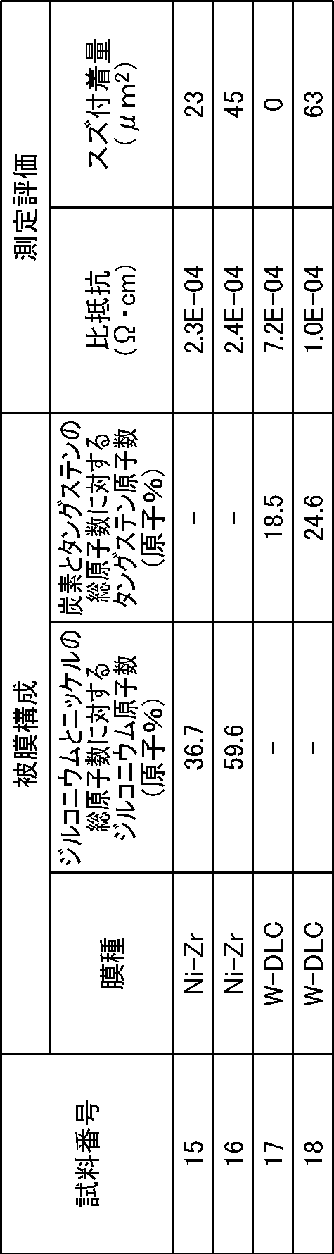
また、表2には銅-ジルコニウム皮膜と同様にアモルファス構造が得られやすいニッケル-ジルコニウム皮膜の測定評価結果を、試料15,16として比較のために示す。表2の結果から、ニッケル-ジルコニウム皮膜ではスズの付着が発生することが分かった。これはニッケル-ジルコニウム皮膜が、アモルファス構造を銅-ジルコニウム皮膜よりも得られにくいからであると考えられる。また、結晶性成分が残るために表面粗さが増し、スズの付着が発生したものと考えられる。
さらに、タングステン含有ダイヤモンドライクカーボン皮膜の測定評価結果についても、表2に試料17,18として示す。タングステン量が18.5原子%である試料17は、スズの付着が発生しないが、比抵抗値においては上記銅-ジルコニウム合金よりも非常に高かった。一方で、比抵抗を下げるためにタングステン含有量24.6原子%に上げた試料18は、スズの付着が発生してしまった。
[実施例2]
上記実施例1と同様の方法で、ターゲットには1つの銅-ジルコニウム複合ターゲットを用いて(1つのターゲットは使用せず)銅-ジルコニウム皮膜を成膜した試料(試料番号19~24)を形成した。ターゲットにはジルコニウム内に銅を埋めこんだジルコニウム-銅の複合ターゲットを用いて、ターゲット印加電力が2.0kWで成膜を実施した。成膜時には基材ステージの回転を行い、基材内での組成ムラが無いように成膜を行った。なお、成膜ガスにはアルゴンガスを用い、炭化水素ガスを用いていないため炭素成分は含んでいない。
上記実施例1と同様の方法で、ターゲットには1つの銅-ジルコニウム複合ターゲットを用いて(1つのターゲットは使用せず)銅-ジルコニウム皮膜を成膜した試料(試料番号19~24)を形成した。ターゲットにはジルコニウム内に銅を埋めこんだジルコニウム-銅の複合ターゲットを用いて、ターゲット印加電力が2.0kWで成膜を実施した。成膜時には基材ステージの回転を行い、基材内での組成ムラが無いように成膜を行った。なお、成膜ガスにはアルゴンガスを用い、炭化水素ガスを用いていないため炭素成分は含んでいない。
なお、試料19~24は、それぞれ成膜時間を制御することで膜厚を変化させた皮膜とした。また、これらの製法で成膜した皮膜は、全て銅とジルコニウムの合計に対するジルコニウム原子数の割合が47.0原子%である。
表3には各試料の評価を示す。
(結果)
結果を表3に示した。
結果を表3に示した。

表3の結果から、銅-ジルコニウム皮膜の膜厚が2.89μm以下である試料19~22は、スズ付着は発生しなかった。しかしながら、膜厚が3.11μmである試料23は、微量のスズ付着が発生した。さらに、膜厚が5.24μmである試料24は、スズの付着量がさらに多くなった。これは表面が平滑な銅-ジルコニウム皮膜であっても、膜厚を厚くすることで表面の粗さが増加したためにスズの付着が発生したものと考えられる。
本明細書は、上記のように様々な態様の技術を開示しているが、そのうち主な技術を以下に纏める。
本発明の第一の主題は、導電性基材と、銅およびジルコニウムを含有する銅-ジルコニウム皮膜とを含む半導体検査装置用プローブピンであって、前記銅-ジルコニウム皮膜において、ジルコニウムと銅の総原子数に対するジルコニウム原子数の割合が15~85原子%であり、前記皮膜の膜厚が、0.05~3μmであることを特徴とする半導体検査装置用プローブピンである。
このような構成によれば、導電性基材表面に形成される導電性皮膜は、前記導電性皮膜の外表面へのスズ凝着性を著しく低減させることができ、これにより、半導体検査装置用プローブピンの不具合発生を低下させて、高寿命化を図ることができる。
前記半導体検査装置用プローブピンにおいて、前記銅-ジルコニウム皮膜がさらに炭素原子を含み、前記銅-ジルコニウム皮膜の総原子数に対する炭素原子数の割合が40原子%以下であることが好ましい。
このような構成によれば、前記導電性皮膜の外表面へのスズ凝着性をさらに低減させることができる。
前記半導体検査装置用プローブピンにおいて、銅-ジルコニウム皮膜が、気相成膜法によって形成されることが好ましい。
このような構成によれば、アモルファス状態の皮膜を容易に得ることができる。
また、本発明の第二の主題は、導電性基材を含む半導体検査装置用プローブピンを製造する方法であって、ターゲットを用いてスパッタリングを行うことにより、前記導電性基材上に、銅およびジルコニウムを含有する銅-ジルコニウム皮膜を形成し、前記銅-ジルコニウム皮膜において、ジルコニウムと銅の総原子数に対するジルコニウム原子数の割合が15~85原子%であり、膜厚が0.05~3μmであることを特徴とする半導体検査装置用プローブピンの製造方法である。
このような製造方法によれば、はんだ中のスズがプローブピンの接触部に凝着するのを防ぐことができ、耐スズ凝着性に優れたアモルファス状態の銅-ジルコニウム皮膜を、半導体検査装置用コンタクトプローブピンの基材上に効果的にかつ容易に形成することができる。
前記導電性基材を含む半導体検査装置用プローブピンを製造する方法において、ターゲットを用いて炭素を含む反応性ガス中でスパッタリングを行うことにより、前記導電性基材上に、銅、ジルコニウム、及び炭素を含有する銅-ジルコニウム-炭素皮膜を形成する半導体検査装置用プローブピンの製造方法であって、前記銅-ジルコニウム-炭素皮膜におけるジルコニウム原子数が、ジルコニウムと銅の総原子数に対して15~85原子%であり、前記炭素原子の数が、前記銅-ジルコニウム-炭素皮膜の総原子数に対して40原子%以下であり、膜厚が0.05~3μmであることが好ましい。
このような構成によれば、前記導電性皮膜の外表面へのスズ凝着性をさらに低減させる製造方法を提供することができる。
前記製造方法において、前記スパッタリングが、アンバランストマグネトロンスパッタリングであることが好ましい。
このような構成によれば、銅-ジルコニウム皮膜の表面性状が、平滑な銅-ジルコニウム皮膜を基材上に形成することができる。
また、本発明の第三の主題は、前記半導体検査装置用プローブピンの先端を、半導体素子の通電部に存在するはんだに接触させ、前記半導体素子の動作確認を行う半導体検査方法である。
このような構成によれば、はんだ中のスズがプローブピンの接触部に凝着せずに、半導体素子の動作確認を長期間行うことができる。
本発明によれば、プローブピンがはんだと接触した際に、はんだの主成分であるスズがプローブピンの接触部に凝着することを防ぎ、耐スズ凝着性に優れた導電性皮膜を基材表面に形成して成る半導体検査装置用プローブピンを提供することができる。
Claims (7)
- 導電性基材と、銅およびジルコニウムを含有する銅-ジルコニウム皮膜とを含む半導体検査装置用プローブピンであって、
前記銅-ジルコニウム皮膜において、ジルコニウムと銅の総原子数に対するジルコニウム原子数の割合が15~85原子%であり、
前記皮膜の膜厚が、0.05~3μmであることを特徴とする半導体検査装置用プローブピン。 - 前記銅-ジルコニウム皮膜がさらに炭素原子を含み、
前記銅-ジルコニウム皮膜の総原子数に対する炭素原子数の割合が、40原子%以下であることを特徴とする請求項1に記載の半導体検査装置用プローブピン。 - 前記銅-ジルコニウム皮膜が、気相成膜法によって形成されたことを特徴とする請求項1に記載の半導体検査装置用プローブピン。
- 導電性基材を含む半導体検査装置用プローブピンを製造する方法であって、
ターゲットを用いてスパッタリングを行うことにより、前記導電性基材上に、銅およびジルコニウムを含有する銅-ジルコニウム皮膜を形成し、
前記銅-ジルコニウム皮膜において、ジルコニウムと銅の総原子数に対するジルコニウム原子数の割合が15~85原子%であり、膜厚が0.05~3μmであることを特徴とする半導体検査装置用プローブピンの製造方法。 - 導電性基材を含む半導体検査装置用プローブピンを製造する方法であって、
ターゲットを用いて炭素を含む反応性ガス中でスパッタリングを行うことにより、前記導電性基材上に、銅、ジルコニウム、及び炭素を含有する銅-ジルコニウム-炭素皮膜を形成する半導体検査装置用プローブピンの製造方法であって、
前記銅-ジルコニウム-炭素皮膜におけるジルコニウム原子数が、ジルコニウムと銅の総原子数に対して15~85原子%であり、
前記炭素原子の数が、前記銅-ジルコニウム-炭素皮膜の総原子数に対して40原子%以下であり、
膜厚が0.05~3μmであることを特徴とする請求項4に半導体検査装置用プローブピンの製造方法。 - 前記スパッタリングが、アンバランストマグネトロンスパッタリングである請求項4または5に記載の製造方法。
- 請求項1~3のいずれかに記載の半導体検査装置用プローブピンの先端を、半導体素子の通電部に存在するはんだに接触させ、前記半導体素子の動作確認を行う半導体検査方法。
Applications Claiming Priority (4)
| Application Number | Priority Date | Filing Date | Title |
|---|---|---|---|
| JP2010161086 | 2010-07-15 | ||
| JP2010-161086 | 2010-07-15 | ||
| JP2011137406A JP5730681B2 (ja) | 2010-07-15 | 2011-06-21 | 半導体検査装置用プローブピン、その製造方法及び半導体検査方法 |
| JP2011-137406 | 2011-06-21 |
Publications (1)
| Publication Number | Publication Date |
|---|---|
| WO2012008128A1 true WO2012008128A1 (ja) | 2012-01-19 |
Family
ID=45469146
Family Applications (1)
| Application Number | Title | Priority Date | Filing Date |
|---|---|---|---|
| PCT/JP2011/003911 Ceased WO2012008128A1 (ja) | 2010-07-15 | 2011-07-07 | 半導体検査装置用プローブピン、その製造方法及び半導体検査方法 |
Country Status (3)
| Country | Link |
|---|---|
| JP (1) | JP5730681B2 (ja) |
| TW (1) | TW201217792A (ja) |
| WO (1) | WO2012008128A1 (ja) |
Families Citing this family (3)
| Publication number | Priority date | Publication date | Assignee | Title |
|---|---|---|---|---|
| JPH078603B2 (ja) | 1985-06-29 | 1995-02-01 | 横浜ゴム株式会社 | 乗用車用空気入りラジアルタイヤ |
| IT1219241B (it) | 1988-04-27 | 1990-05-03 | Firestone Int Dev Spa | Pneumatico radiale per veicoli |
| RU2724301C2 (ru) * | 2018-12-17 | 2020-06-22 | Акционерное общество "НПО "Орион" | Способ увеличения прочности зондов многозондовых головок |
Citations (3)
| Publication number | Priority date | Publication date | Assignee | Title |
|---|---|---|---|---|
| JP2000317900A (ja) * | 1999-05-07 | 2000-11-21 | Tokyo Inst Of Technol | 薄膜構造体の製造方法 |
| JP2002277485A (ja) * | 2001-03-19 | 2002-09-25 | Akira Shimokawabe | プローブカード、プローブピン、プローブカード製造方法及びプローブピン製造方法 |
| JP2006082191A (ja) * | 2004-09-16 | 2006-03-30 | Sumitomo Electric Hardmetal Corp | 表面被覆切削工具 |
-
2011
- 2011-06-21 JP JP2011137406A patent/JP5730681B2/ja active Active
- 2011-07-07 WO PCT/JP2011/003911 patent/WO2012008128A1/ja not_active Ceased
- 2011-07-14 TW TW100124983A patent/TW201217792A/zh unknown
Patent Citations (3)
| Publication number | Priority date | Publication date | Assignee | Title |
|---|---|---|---|---|
| JP2000317900A (ja) * | 1999-05-07 | 2000-11-21 | Tokyo Inst Of Technol | 薄膜構造体の製造方法 |
| JP2002277485A (ja) * | 2001-03-19 | 2002-09-25 | Akira Shimokawabe | プローブカード、プローブピン、プローブカード製造方法及びプローブピン製造方法 |
| JP2006082191A (ja) * | 2004-09-16 | 2006-03-30 | Sumitomo Electric Hardmetal Corp | 表面被覆切削工具 |
Also Published As
| Publication number | Publication date |
|---|---|
| JP2012037506A (ja) | 2012-02-23 |
| JP5730681B2 (ja) | 2015-06-10 |
| TW201217792A (en) | 2012-05-01 |
Similar Documents
| Publication | Publication Date | Title |
|---|---|---|
| JP5667350B2 (ja) | コンタクトプローブピン | |
| US9116173B2 (en) | Contact probe having carbon film on surface thereof | |
| JP5301515B2 (ja) | 電気的接点部材 | |
| US9625492B2 (en) | Contact probe pin | |
| JP5730681B2 (ja) | 半導体検査装置用プローブピン、その製造方法及び半導体検査方法 | |
| JP5049358B2 (ja) | 半導体検査装置用コンタクトプローブピンの基材上にタングステン含有ダイヤモンドライクカーボン皮膜を製造する方法 | |
| TWI457570B (zh) | Electrical contact components | |
| JP5568268B2 (ja) | 半導体検査装置用コンタクトプローブピン | |
| JP5535131B2 (ja) | 半導体検査装置用プローブピン及びその製造方法 | |
| JP7457638B2 (ja) | 摺接部材、導電性高硬度保護被膜及び摺接部材の製造方法 | |
| JP2025018861A (ja) | 原子間力顕微鏡用プローブ及び鋼材の評価方法 |
Legal Events
| Date | Code | Title | Description |
|---|---|---|---|
| 121 | Ep: the epo has been informed by wipo that ep was designated in this application |
Ref document number: 11806463 Country of ref document: EP Kind code of ref document: A1 |
|
| NENP | Non-entry into the national phase |
Ref country code: DE |
|
| 122 | Ep: pct application non-entry in european phase |
Ref document number: 11806463 Country of ref document: EP Kind code of ref document: A1 |