WO2012004982A1 - 携帯無線機 - Google Patents
携帯無線機 Download PDFInfo
- Publication number
- WO2012004982A1 WO2012004982A1 PCT/JP2011/003841 JP2011003841W WO2012004982A1 WO 2012004982 A1 WO2012004982 A1 WO 2012004982A1 JP 2011003841 W JP2011003841 W JP 2011003841W WO 2012004982 A1 WO2012004982 A1 WO 2012004982A1
- Authority
- WO
- WIPO (PCT)
- Prior art keywords
- circuit board
- closed state
- ground conductor
- antenna element
- housing
- Prior art date
- Legal status (The legal status is an assumption and is not a legal conclusion. Google has not performed a legal analysis and makes no representation as to the accuracy of the status listed.)
- Ceased
Links
Images




Classifications
-
- H—ELECTRICITY
- H01—ELECTRIC ELEMENTS
- H01Q—ANTENNAS, i.e. RADIO AERIALS
- H01Q1/00—Details of, or arrangements associated with, antennas
- H01Q1/12—Supports; Mounting means
- H01Q1/22—Supports; Mounting means by structural association with other equipment or articles
- H01Q1/24—Supports; Mounting means by structural association with other equipment or articles with receiving set
- H01Q1/241—Supports; Mounting means by structural association with other equipment or articles with receiving set used in mobile communications, e.g. GSM
- H01Q1/242—Supports; Mounting means by structural association with other equipment or articles with receiving set used in mobile communications, e.g. GSM specially adapted for hand-held use
- H01Q1/243—Supports; Mounting means by structural association with other equipment or articles with receiving set used in mobile communications, e.g. GSM specially adapted for hand-held use with built-in antennas
-
- H—ELECTRICITY
- H01—ELECTRIC ELEMENTS
- H01Q—ANTENNAS, i.e. RADIO AERIALS
- H01Q1/00—Details of, or arrangements associated with, antennas
- H01Q1/48—Earthing means; Earth screens; Counterpoises
-
- H—ELECTRICITY
- H01—ELECTRIC ELEMENTS
- H01Q—ANTENNAS, i.e. RADIO AERIALS
- H01Q9/00—Electrically-short antennas having dimensions not more than twice the operating wavelength and consisting of conductive active radiating elements
- H01Q9/04—Resonant antennas
- H01Q9/30—Resonant antennas with feed to end of elongated active element, e.g. unipole
- H01Q9/42—Resonant antennas with feed to end of elongated active element, e.g. unipole with folded element, the folded parts being spaced apart a small fraction of the operating wavelength
-
- H—ELECTRICITY
- H04—ELECTRIC COMMUNICATION TECHNIQUE
- H04M—TELEPHONIC COMMUNICATION
- H04M1/00—Substation equipment, e.g. for use by subscribers
- H04M1/02—Constructional features of telephone sets
- H04M1/0202—Portable telephone sets, e.g. cordless phones, mobile phones or bar type handsets
- H04M1/0206—Portable telephones comprising a plurality of mechanically joined movable body parts, e.g. hinged housings
- H04M1/0208—Portable telephones comprising a plurality of mechanically joined movable body parts, e.g. hinged housings characterized by the relative motions of the body parts
- H04M1/021—Portable telephones comprising a plurality of mechanically joined movable body parts, e.g. hinged housings characterized by the relative motions of the body parts using combined folding and rotation motions
- H04M1/0212—Portable telephones comprising a plurality of mechanically joined movable body parts, e.g. hinged housings characterized by the relative motions of the body parts using combined folding and rotation motions with a two degrees of freedom mechanism, i.e. folding around a first axis and rotating around a second axis perpendicular to the first
Definitions
- the present invention relates to a portable wireless device such as a mobile phone, and more particularly to a foldable portable wireless device having a rotating two-axis structure.
- wireless systems with relatively narrow bandwidths such as GPS (Global Positioning System), WLAN (Wireless LAN), Bluetooth (registered trademark), etc. It is becoming.
- wireless systems with relatively narrow bandwidths such as GPS (Global Positioning System), WLAN (Wireless LAN), Bluetooth (registered trademark), etc. It is becoming.
- a plurality of wireless systems a plurality of antenna elements are also mounted.
- FIG. 12 is a perspective view showing an appearance of a conventional foldable portable wireless device 100 adopting a rotating biaxial structure.
- A) of the figure shows a normally closed state
- (b) shows an opened state
- (c) shows an inverted closed state.
- the portable wireless device 100 adopting the rotating biaxial structure includes three housings (a first housing 101, a second housing 102, and a third housing 103).
- a connecting portion between the first housing 101 and the second housing 102 is provided with a first hinge (not shown), and the first housing 101 and the second housing 102 are connected to each other by the first hinge so as to be freely opened and closed. Is done.
- a connecting portion between the second casing 102 and the third casing 103 is provided with a second hinge (not shown), and the second casing 102 and the third casing 103 are rotatable by the second hinge. Connected.
- a liquid crystal display 105 is provided in the third housing 103. As the liquid crystal display 105 is enlarged, a reinforcing metal sheet (not shown) for securing strength may be provided in the third housing 103 in some cases.
- a cellular phone employing the above-described rotating biaxial structure can ensure uniform antenna performance in two closed states, a normal closed state and an inverted closed state.
- portable wireless devices described in Patent Documents 1 and 2.
- antenna elements are arranged on each of a liquid crystal display side in a rotating third housing and an inner wall surface side facing the liquid crystal display. In this way, in each of the two closed states, even if one antenna element approaches the first housing side, the other antenna element is separated from the first housing, so that deterioration in antenna performance is kept low. be able to.
- the portable wireless device described in Patent Document 2 is provided with an antenna element in a first casing and a feeding circuit at each end of the antenna element, while a second casing (in the above-described third casing). Equivalently) a conductive part is provided, and in each of the two closed states, the power feeding circuit is switched so that the conductive part is on the power feeding circuit side of the antenna element while the antenna element and the conductive part are close to each other. . In this way, the antenna performance can be made uniform in the two closed states.
- the present invention has been made in view of such circumstances, and in a folding portable wireless device adopting a rotating biaxial structure, stable antenna performance can be ensured in two closed states, a normal closed state and an inverted closed state.
- an object is to provide a portable wireless device capable of reducing the thickness and size of the device body.
- the portable wireless device of the present invention includes a first housing, a second housing, a first hinge that connects the first housing and the second housing so as to be openable and closable, a third housing, A second hinge rotatably connecting the second housing and the third housing; a first circuit board provided in the first housing and functioning as a first ground conductor; and the third housing A second circuit board provided on the antenna, an antenna element having a feeding portion connected to one surface of the second circuit board, a second ground conductor formed on the other surface of the second circuit board, A signal cable that electrically connects the first circuit board and the second circuit board; and in a normally closed state where the first surface of the third casing faces the first casing, the power feeding unit And the second ground conductor is disposed between a part of the antenna element and the first ground conductor, and is opposite to the first surface of the third housing.
- the second side face each other inverted closed and the first housing state of a portion of the feeding portion and the antenna element is disposed between the first ground conductor and said second
- the second ground conductor in the normally closed state, is disposed between the feeding portion and part of the antenna element and the first ground conductor, and in the inverted closed state, the second ground conductor is one of the feeding portion and the antenna element.
- the portion is disposed between the first ground conductor and the second ground conductor. Therefore, the distance between the feeding part, part of the antenna element, and the second ground conductor is constant in two states, the normal closed state and the inverted closed state, and current concentrates on the feeding part and part of the antenna element.
- a change in impedance due to a change in the distance between the first casing and the first circuit board can be suppressed from the antenna element in the closed state, and stable antenna performance can be ensured in the two closed states of the normal closed state and the inverted closed state.
- the antenna performance is improved by reducing the distance between the power feeding unit and a part of the antenna element and the second circuit board. Therefore, the second circuit board can be thinned, and the device main body can be thinned and compact. Can be achieved.
- the antenna element has a flat plate shape.
- the overlapping area between the power feeding unit and a part of the antenna element and the second ground conductor is increased, and the current is further concentrated on the power feeding unit and a part of the antenna element. More stable antenna performance can be secured in the two closed states.
- the first circuit board and the first circuit board are arranged so as to overlap each other in a front view.
- the antenna element has a flat-plate-like orthogonal part orthogonal to the second circuit board, and the interval between the orthogonal part and the first circuit board is substantially the same in the normally closed state and the inverted closed state. It is characterized by that.
- a part of the antenna element is formed as a flat orthogonal portion orthogonal to the second circuit board, and the overlapping area between the antenna element and the first circuit board is minimized, so that the first circuit exerted on the antenna element is reduced.
- the influence of the substrate can be reduced.
- the interval between the orthogonal portion and the first circuit board is substantially the same in the normal closed state and the inverted closed state, stable antenna performance can be ensured in the two closed states.
- the second circuit board is arranged so that the distance between the second circuit board and the first circuit board is substantially the same in a normally closed state and an inverted closed state.
- a conductive member that is electrically connected to the second circuit board and is different from the second circuit board is provided as a second ground conductor.
- the dedicated second ground conductor since the dedicated second ground conductor is provided, for example, it is possible to enlarge a reinforcing plate for preventing destruction of the liquid crystal display device, and it is possible to easily ensure the strength. Further, depending on the size of the second ground conductor, the current flowing through the second circuit board and the second ground conductor can be changed to improve the antenna performance.
- a foldable portable wireless device adopting a rotating two-axis structure
- stable antenna performance can be ensured in two closed states, that is, a normal closed state and an inverted closed state, and the device body can be made thinner and smaller. Can be achieved.
- FIG. 1 The perspective view which shows the external appearance of the portable radio
- A), (b) It is a figure which shows an internal structure when the portable radio
- (a) is front perspective drawing which shows an internal structure at the time of front view,
- (b) is Diagram showing the internal structure when viewed from the side (A), (b) It is a figure which shows an internal structure when the portable radio
- wireless machine of FIG. The graph which shows the efficiency calculation result when changing the space between the feeding part of the antenna element and the second ground conductor by simulation analysis Diagram showing current distribution density in normally closed state by simulation analysis Diagram showing current distribution density in inverted closed state by simulation analysis (A)-(c)
- FIGS. 1A and 1B are perspective views showing the appearance of the portable wireless device according to Embodiment 1 of the present invention.
- the portable wireless device 1 of the present embodiment is a foldable mobile phone that employs a rotating biaxial structure, and includes a first case 10, a second case 11, and a third case 12. It is made up of a housing and can take three states: “normally closed state”, “open state”, and “inverted closed state”.
- the first casing 10 and the second casing 11 are connected to each other by a first hinge 20 so as to be opened and closed.
- the second casing 11 and the third casing 12 are rotatable by a second hinge (rotating biaxial hinge) 21. It is connected.
- the first hinge 20 is provided between the first housing 10 and the second housing 11, and the second hinge 21 is provided between the second housing 11 and the third housing 12.
- the third housing 12 is provided with a liquid crystal display 15, and the third housing 10 is provided with an antenna element (not shown).
- the first casing 10 is provided with a first circuit board 13, and the third casing 12 is provided with a second circuit board 14.
- the first circuit board 13 is used as the first ground conductor. Details of the first ground conductor will be described later.
- the first circuit board 13 and the second circuit board 14 are connected by a signal cable 30.
- a thin coaxial cable group is mainly used.
- the thin coaxial cable group is a group of coaxial cables having a plurality of thin diameters arranged in a cylindrical shape and bundled with tape or the like.
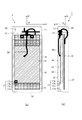
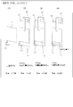
- FIG. 2 is a diagram showing an internal structure when the portable wireless device 1 of the present embodiment is in a “normally closed state”, and (a) is a front perspective view showing the internal structure when viewed from the front. ) Is a diagram showing the internal structure when viewed from the side. Especially in the case of (b), it is a figure which shows the internal structure seen from the right side toward drawing of (a).
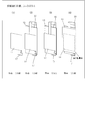
- FIG. 3 is a diagram showing the internal structure when the portable wireless device 1 of the present embodiment is in the “inverted closed state”.
- FIG. 3A is a front perspective view showing the internal structure when viewed from the front.
- (b) it is a figure which shows the internal structure seen from the right side toward drawing of (a).
- the third casing 12 includes the second circuit board 14 in addition to the second circuit board 14 and the liquid crystal display 15 described above.
- a larger flat plate-like second ground conductor 16 and an antenna element 17 are provided.
- the second ground conductor 16 is a flat metal plate having good conductivity.
- the length of the second ground conductor 16 in the short direction is shorter than the length of the third housing 12 in the short direction, and is longer than the length of the second circuit board 14 in the short direction. Is shorter than the length of the third casing 12 in the longitudinal direction and longer than the length of the second circuit board 14 in the longitudinal direction.
- the second ground conductor 16 is laminated on the second circuit board 14 and is electrically connected to the ground of the second circuit board 14.
- the second ground conductor 16 is not necessarily laminated on the second circuit board 14 and may be disposed adjacent to the second circuit board 14.
- the second ground conductor 16 may be constituted by a reinforcing plate arranged on the liquid crystal display 15, and this reinforcing plate may be arranged on the antenna element 17 and the back surface of the feeding portion 17 a of the antenna element 17.
- the antenna element 17 is disposed at the upper left corner portion (the lower left corner portion in FIG. 2A) of the second circuit board 14 on the side surface opposite to the surface to which the second ground conductor 16 is connected.
- the antenna element 17 is composed of four consecutive parts including a feeding part 17a, a parallel running part 17b, a non-parallel running part 17c, and an orthogonal part 17d.
- the power feeding unit 17 a is connected to a wireless circuit (not shown) mounted on the second circuit board 14.
- the feeding portion 17a and the parallel running portion 17b of the antenna element 17 are portions parallel to the second ground conductor 16 in the y direction in FIGS. 2B and 3B, and are shown in FIGS.
- the non-parallel portion 17c of the antenna element 17 is a portion that is not parallel to the second ground conductor 16 in the y direction of FIGS. 2B and 3B, and FIGS. 2A and 3B.
- the tip of the second ground conductor 16 is located at the boundary where the parallel portion 17b changes to the non-parallel portion 17c. Between 17d is the non-parallel portion 17c.
- the orthogonal portion 17d of the antenna element 17 is a portion that is bent at a right angle with respect to the portions up to the power feeding portion 17a, the parallel running portion 17b, and the non-parallel running portion 17c, and is bent in a direction toward the center of the tip of the second circuit board 14. It has a shape. As shown in FIG. 2A, the antenna element 17 is located on the left side when the portable wireless device 1 is in the normally closed state. Since 12 rotates 180 degrees, it is located on the right side as shown in FIG.
- FIG. 4 is a perspective view showing the appearance of the antenna element 17.
- FIGS. 9A and 9B are views in which the way of viewing the antenna element 17 is changed by 180 degrees.
- the antenna element 17 includes a feeding portion 17a and a parallel running portion 17b connected through a step, and the parallel running portion 17b and the non-parallel running portion 17c are configured on the same surface. Further, the non-parallel portion 17c and the orthogonal portion 17d are connected at an angle of 90 degrees.
- the orthogonal part 17d is bent stepwise at three places.
- the power feeding portion 17a, the parallel running portion 17b, and the non-parallel running portion 17c are connected to the second circuit board 14.
- the second ground conductor 16 and the first circuit board 13 are disposed so as to be parallel to the plane portion, and the orthogonal portion 17d is disposed so as to be orthogonal.
- FIG. 5 is an enlarged view of a portion where the antenna element 17 of the portable wireless device 1 is normally closed. Each dimension in FIG. 5 is listed below. Note that “ ⁇ ” indicates a wavelength at the design frequency, and in this embodiment, it is a 1.5 GHz band used in GPS (Global Positioning System).
- Da Distance between the power feeding portion 17a and the second ground conductor 16 0.002 ⁇
- Db1 Distance between the parallel running portion 17b and the second ground conductor 16 0.006 ⁇
- Dc Distance between the non-parallel portion 17c and the first circuit board 13 0.037 ⁇
- Dd Distance between the orthogonal part 17d and the first circuit board 13 0.022 ⁇
- Dg distance between the second ground conductor 16 and the first circuit board 13 0.029 ⁇
- La Length of the power feeding portion 17a 0.015 ⁇
- Lb Length of the parallel running portion 17b 0.020 ⁇
- Lc Length of the non-parallel portion 17c 0.007 ⁇
- Wa The width of the power feeding portion 17a is 0.015 ⁇ .
- Wb width of parallel running portion 17b 0.010 ⁇
- Wc width of the non-parallel portion 17c 0.010 ⁇
- Wd width of the orthogonal part 17d 0.015 ⁇
- the distance Da between the power feeding unit 17 a and the second ground conductor 16 corresponds to the thickness of the second circuit board 14.
- FIG. 6 is an enlarged view of an arrangement portion of the antenna element 17 of the portable wireless device 1 in the inverted closed state. Each dimension in FIG. 6 is listed below.
- Da Distance between the power feeding portion 17a and the second ground conductor 16 0.002 ⁇
- Db1 Distance between the parallel running portion 17b and the second ground conductor 16 0.006 ⁇
- Dc Distance between the non-parallel portion 17c and the first circuit board 13 0.018 ⁇
- Dd distance between the orthogonal portion 17d and the first circuit board 13 0.018 ⁇
- Dg interval between the second ground conductor 16 and the first circuit board 13 0.031 ⁇
- La Length of the power feeding portion 17a 0.015 ⁇
- Lb Length of the parallel running portion 17b 0.020 ⁇
- Lc Length of the non-parallel portion 17c 0.007 ⁇
- Wa The width of the power feeding portion 17a is 0.015 ⁇ .
- Wb width of parallel running portion 17b 0.010 ⁇
- Wc width of the non-parallel portion 17c 0.010 ⁇
- Wd width of the orthogonal part 17d 0.015 ⁇
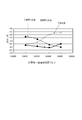
- FIG. 7 is a graph showing a measurement result of the antenna efficiency when the distance Da between the power feeding portion 17a and the second ground conductor 16, that is, the thickness of the second circuit board 14 is changed.
- the respective dimensions in the normally closed state of the portable wireless device 1 are as follows.
- the dimensions of the portable wireless device 1 in the inverted closed state are as follows.
- the distance Dc between the non-parallel portion 17c and the first circuit board 13 is 0.037 ⁇ . At this time, if the distance Da is reduced from 0.002 ⁇ to 0.001 ⁇ , the efficiency is An improvement of 0.6 dB can be seen. On the other hand, in the inverted closed state, the interval Dc is 0.0018 ⁇ , which is smaller than that in the normal closed state. At this time, if the interval Da is decreased from 0.002 ⁇ to 0.001 ⁇ , the efficiency is about 1. An improvement of 5 dB is obtained. The smaller the interval Dc and the smaller the interval Da, the better the efficiency.
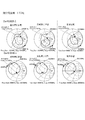
- Fig. 8 shows the impedance characteristics during the above measurement.
- the upper stage of FIG. 8 is the case where the interval Da between the power supply unit 17a and the second ground conductor 16 is 0.0025 ⁇ , and the lower stage is the case where the interval Da is reduced to 0.0010 ⁇ .
- the impedance in the inverted closed state and the open state is shown.
- the ⁇ mark indicates the impedance at 1.58 GHz.
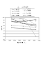
- FIG. 9 shows efficiency calculation results when four models are analyzed by simulation.
- FIG. 10 and FIG. 11 show the four analysis models and the current distribution density when the distance Da between the power feeding unit 17a and the second ground conductor 16 is 0.002 ⁇ . Note that the analysis model in a portion not particularly described is substantially the same as the above-described dimensions, but the frequency is in the 2.5 GHz band. 10 is a normally closed state, and FIG. 11 is an inverted closed state. The four analysis models will be described with reference to FIGS. 10 and 11.
- FIGS. 10 and 11 show respective analysis models. Note that FIG. 10 and FIG. 11 are the only differences between the normal closed state and the inverted closed state.
- the analysis model (1) includes only the antenna element 17 and the second circuit board 14, and is an ideal state in which there are no obstacles that obstruct the antenna element.
- the analysis model (2) the first circuit board 13 and the signal cable 30 are added to the analysis model (1), and the power feeding section 17a and the parallel running section 17b are projected from the front view in the second circuit board 14 and the second circuit board. It does not overlap with the ground conductor.
- the analysis model (3) extends the ground portion of the second circuit board 14 from the analysis model (2) so that the ground overlaps with the power feeding portion 17a and the parallel running portion 17b when projected from the front. Is the same as the antenna element width.
- the analysis model (4) is obtained by adding a metal plate different from the second circuit board as the second ground conductor to the analysis model (1), and is the same as the actual measurement model.
- the efficiency calculation result in the normally closed state is indicated by a solid line
- the efficiency calculation result in the inverted closed state is indicated by a broken line.
- the analysis models (1), (2), (3), and (4) are indicated by ⁇ mark, X mark, ⁇ mark, and ⁇ mark, respectively.
- the analysis model (1) since the analysis model (1) is not affected by the obstacle, the efficiency change due to the interval Da is slight.
- the analysis model (2) the degradation of 0.4 dB occurs from the analysis model (1) due to the influence of the first circuit board, but the efficiency change due to the interval Da is about 0.1 dB and is slight.
- the analysis model (3) has the configuration of the present invention, and an improvement effect of 0.5 dB or more is obtained when the interval Da is set to 0.007 ⁇ or less with respect to the analysis model (2).
- the analysis model (4) is an embodiment of the present invention, and it can be seen that the best efficiency is obtained among the four analysis models when the interval Da is about 0.003 ⁇ .
- the analysis result and the actual measurement data have the same configuration as the above-described actual measurement data, and the efficiency is improved as the interval Da is reduced, and a result supporting the actual measurement data is obtained.
- the interval Da is 0.003 ⁇ .
- the current concentrates on the antenna element, but in the analysis models (3) and (4), the second ground that overlaps the feeding unit 17a and the parallel running unit 17b by projection in front view.
- the ground current around the conductor increases. Further, the current of the second ground conductor and the signal cable 30 is increased, and the efficiency is improved by the increase in radiation from the ground of the second ground conductor and the signal cable.
- FIG. 11 shows the current distribution in the inverted closed state.
- the interval Da is also 0.003 ⁇ .
- the same tendency as in the normally closed state shown in FIG. 10 is observed, and the efficiency is improved by increasing the radiation from the second ground conductor.
- the performance in the inverted closed state is improved without causing the performance deterioration in the normal closed state. Is possible. Thereby, the thickness of the second circuit board 14 can be reduced.
- the second ground conductor 16 in the normally closed state, is between the power feeding portion 17a and part of the antenna element 17 and the first circuit board 13 that is the first ground conductor.
- the inverted closed state a part of the power feeding portion 17a and the antenna element 17 are disposed between the first circuit board 13 and the second ground conductor 16 which are the first ground conductors. Therefore, the distance between the feeding portion 17a and a part of the antenna element 17 and the second ground conductor 16 is constant in two states, a normal closed state and an inverted closed state, and current flows in the feeding portion 17a and a part of the antenna element 17.
- the antenna performance is improved by reducing the distance between the power supply unit 17a and a part of the antenna element 17 and the second circuit board 14, so that the second circuit board 14 can be thinned, and the device main body can be reduced. Thinning and miniaturization can be achieved.
- the second circuit board 14 provided in the third housing 12 and the power feeding unit 17a is connected to one surface of the second circuit board 14.
- An antenna element 17, a second ground conductor 16 connected to the other surface of the second circuit board 14, and a signal cable 30 for electrically connecting the first circuit board 13 and the second circuit board 14 are provided.
- the second ground conductor 16 is disposed between the power feeding portion 17a and a part of the antenna element 17 and the first circuit board 13 as the first ground conductor, and in the inverted closed state, the power feeding portion 17a and Since a part of the antenna element 17 is arranged between the first circuit board 13 which is the first ground conductor and the second ground conductor 16, stable antenna performance can be achieved in two closed states, a normal closed state and an inverted closed state. It can be secured.
- the distance between the power supply unit 17a and a part of the antenna element 17 and the first circuit board 13 is substantially the same in the two closed states, that is, the normal closed state and the inverted closed state, the device body is thinned and miniaturized. Can be planned.
- the first circuit board 13 itself is the first ground conductor, but a conductive member different from the first circuit board 13 is provided as the first ground conductor, You may make it connect electrically. Even in this case, as in the case where the first circuit board 13 itself is the first ground conductor, stable antenna performance can be ensured in the two closed states of the normal closed state and the inverted closed state.
- the present invention has an effect that a stable antenna performance can be secured in two closed states of a normal closed state and an inverted closed state, and the device main body can be thinned and miniaturized. It can be applied to portable wireless devices such as mobile phones.
Landscapes
- Engineering & Computer Science (AREA)
- Computer Networks & Wireless Communication (AREA)
- Support Of Aerials (AREA)
- Telephone Set Structure (AREA)
- Waveguide Aerials (AREA)
Abstract
本発明の課題は、回転2軸構造を採用した折畳み式の携帯無線機において、通常閉じ状態と反転閉じ状態の2つの閉じ状態で安定したアンテナ性能を確保できるとともに、機器本体の薄型化及び小型化が図れる携帯無線機を提供することである。 第3筐体(12)の液晶表示器(15)がある側の第1の面が第1筐体(10)と向かい合う通常閉じ状態において、給電部(17a)及びアンテナ素子(17)の一部と第1地導体である第1回路基板(13)との間に第2地導体(16)を配置し、第3筐体(12)の第1の面と反対の第2の面が第1筐体(10)と向かい合う反転閉じ状態において、第1地導体である第1回路基板(13)と第2地導体(16)との間に給電部(17a)及びアンテナ素子(17)の一部を配置する。
Description
本発明は、携帯電話等の携帯無線機に関し、特に回転2軸構造を持つ折畳み式の携帯無線機に関する。
近年の携帯電話には、セルラ通信用の無線システムの他に、GPS(Global Positioning System)、WLAN(Wireless LAN)、Bluetooth(登録商標)などの比帯域の比較的狭い無線システムが搭載されるようになってきている。また、複数の無線システムを搭載することで、アンテナ素子も複数個搭載されるようになってきている。
また、近年の携帯電話には、待ち受け時では“通常閉じ状態”、通話時では“開き状態”、ワンセグ視聴やタッチパネル操作等の液晶画面が見える状態で閉じる“ビューワ閉じ状態”の3つの状態をとる回転2軸構造(“スィーベル構造”とも呼ばれる)を有したものもある。なお、本明細書では、“ビューワ閉じ状態”のことを“反転閉じ状態”と呼ぶこととする。すなわち、2つの閉じ状態のうち一方を、“通常閉じ状態”と呼び、他方を“反転閉じ状態”と呼ぶ。
図12は、回転2軸構造を採用した従来の折畳み式の携帯無線機100の外観を示す斜視図である。同図の(a)は通常閉じ状態、(b)は開き状態、(c)は反転閉じ状態をそれぞれ示す。図12の(b)に示すように、回転2軸構造を採用した携帯無線機100は、3つの筐体(第1筐体101、第2筐体102、第3筐体103)からなる。第1筐体101と第2筐体102の連結部には第1ヒンジ(図示略)が設けられており、この第1ヒンジによって第1筐体101と第2筐体102が開閉自在に連結される。第2筐体102と第3筐体103の連結部には第2ヒンジ(図示略)が設けられており、この第2ヒンジによって第2筐体102と第3筐体103が回動自在に連結される。第3筐体103には液晶表示器105が設けられている。なお、液晶表示器105の大画面化に伴い、第3筐体103内には強度を確保するための補強用金属板金(図示略)が設けられる場合がある。
上述した回転2軸構造を採用した携帯電話では、通常閉じ状態と反転閉じ状態の2つの閉じ状態で均一なアンテナ性能を確保できることが望まれている。この要望を実現したものとして、例えば特許文献1、2に記載された携帯無線装置がある。特許文献1に記載された携帯無線装置は、回動する第3筐体内の液晶表示器側と該液晶表示器に対向する内壁面側のそれぞれにアンテナ素子を配置している。このようにすることで、2つの閉じ状態のそれぞれにおいて、一方のアンテナ素子が第1筐体側に接近しても、他方のアンテナ素子が第1筐体から離れるので、アンテナ性能の劣化を低く抑えることができる。
他方、特許文献2に記載された携帯無線装置は、第1筐体にアンテナ素子を設けるとともに、該アンテナ素子の両端それぞれに給電回路を設ける一方、第2筐体(上述した第3筐体に相当)に導電性部品を設け、2つの閉じ状態のそれぞれにおいて、アンテナ素子と導電性部品が接近する状態で、導電性部品がアンテナ素子の給電回路側となるように、給電回路の切り替えを行う。このようにすることで、2つの閉じ状態でアンテナ性能の均一化が図れる。
なお、携帯電話の小型化、薄型化及び大画面化は継続して行われている。
しかしながら、回転2軸構造を採用した従来の折畳み式の携帯無線機では、装置の薄型化に伴い、通常閉じ状態と反転閉じ状態で、アンテナ素子から周辺構造物までの必要距離の確保が困難である。また、液晶表示器の大画面化に伴う補強用金属板金の拡大により、アンテナ素子と補強用金属板金との間で必要とする距離の確保と、装置の薄型化に伴う補強用金属板金とアンテナ給電部との間の距離の確保が困難である。
また、特許文献1に記載された携帯無線装置においては、装置本体の薄型化を図ると、2つのアンテナ素子のうち一方のアンテナ素子と第1筐体との距離と、他方のアンテナ素子と第1筐体との距離との差分が小さくなり、アンテナ性能劣化を低減することが困難になる。また、2つのアンテナ素子を必要とするので、そのための空間を確保しなればならず、小型化に限界がある。
また、特許文献2に記載された携帯無線機においては、上記同様に装置本体の薄型化を図るとアンテナ素子が導電性部品に接近するため、アンテナ性能が劣化してしまう。また、切替回路を設けるため、その分、回路基板の面積が大きくなり、小型化に限界がある。
本発明は、係る事情に鑑みてなされたものであり、回転2軸構造を採用した折畳み式の携帯無線機において、通常閉じ状態と反転閉じ状態の2つの閉じ状態で安定したアンテナ性能を確保できるとともに、機器本体の薄型化及び小型化が図れる携帯無線機を提供することを目的とする。
本発明の携帯無線機は、第1筐体と、第2筐体と、前記第1筐体と前記第2筐体とを開閉自在に連結する第1ヒンジと、第3筐体と、前記第2筐体と前記第3筐体とを回動自在に連結する第2ヒンジと、前記第1筐体に設けられ、第1地導体として機能する第1回路基板と、前記第3筐体に設けられた第2回路基板と、前記第2回路基板の一方の面に給電部が接続されたアンテナ素子と、前記第2回路基板の他方の面に構成された第2地導体と、前記第1回路基板と前記第2回路基板とを電気的に接続する信号ケーブルと、を備え、前記第3筐体の第1の面が前記第1筐体と向かい合う通常閉じ状態において、前記給電部及び前記アンテナ素子の一部と前記第1地導体との間に前記第2地導体が配置され、前記第3筐体の前記第1の面と反対の第2の面が前記第1筐体と向かい合う反転閉じ状態において、前記第1地導体と前記第2地導体との間に前記給電部及び前記アンテナ素子の一部が配置される。
上記構成によれば、通常閉じ状態においては、第2地導体が給電部及びアンテナ素子の一部と第1地導体との間に配置され、反転閉じ状態においては、給電部及びアンテナ素子の一部が第1地導体と第2地導体との間に配置される。したがって、給電部とアンテナ素子の一部と第2地導体の間隔は、通常閉じ状態と反転閉じ状態の2つの状態で一定となり、給電部とアンテナ素子の一部に電流が集中し、2つの閉じ状態におけるアンテナ素子から第1筺体と第1回路基板との間隔変化によるインピーダンス変化を抑えることができ、通常閉じ状態と反転閉じ状態の2つの閉じ状態で安定したアンテナ性能を確保できる。また、給電部及びアンテナ素子の一部と第2回路基板との間隔を縮小することにより、アンテナ性能は改善することから、第2回路基板の薄型化が可能となり、機器本体の薄型化及び小型化が図れる。
上記構成において、前記アンテナ素子は、平板状であることを特徴とする。
上記構成によれば、給電部とアンテナ素子の一部と第2地導体との重なる面積が増え、給電部とアンテナ素子の一部に電流が更に集中するため、インピーダンスの変化を更に抑制し、2つの閉じ状態で更に安定したアンテナ性能を確保できる。
上記構成において、前記アンテナ素子のうち、通常閉じ状態において前記第1地導体と前記第2地導体との間に配置されていない前記アンテナ素子の一部が、通常閉じ状態と反転閉じ状態の2つの閉じ状態において、前記第1回路基板と正面視で重なるように配置されていることを特徴とする。
上記構成によれば、アンテナ素子と前記第1回路基板が併走し、正面視で重なる箇所のアンテナ素子の電流が減少しても、第2地導体及び第1地導体の電流が増加するため、アンテナ性能の劣化を抑制することが可能である。
上記構成において、前記アンテナ素子は、前記第2回路基板と直交する平板状の直交部を有し、前記直交部前記第1回路基板との間隔が通常閉じ状態及び反転閉じ状態で略同一であることを特徴とする。
上記構成によれば、アンテナ素子の一部分を第2回路基板と直交する平板状の直交部とし、アンテナ素子と第1回路基板との重なり面積を極小とすることにより、アンテナ素子に及ぼす第1回路基板の影響を低減することが可能となる。また、該直交部と第1回路基板との間隔が通常閉じ状態及び反転閉じ状態で略同一となるようにしたので、2つの閉じ状態で安定したアンテナ性能を確保することが可能となる。
上記構成において、前記第2回路基板は、通常閉じ状態及び反転閉じ状態で前記第1回路基板との間隔が略同一になるように配置されたことを特徴とする。
上記構成によれば、第1回路基板と第2回路基板の電流は通常閉じ状態と反転閉じ状態で略同一となるため、2つの閉じ状態で安定したアンテナ性能を確保することが可能となる。
上記構成において、前記第2回路基板と電気的に接続され、前記第2回路基板とは別の導電性部材を第2地導体として設けたことを特徴とする。
上記構成によれば、専用の第2地導体を設けたので、例えば液晶表示装置の破壊防止の補強板を拡大することが可能となり、強度確保を容易に行うことが可能となる。また、第2地導体の大きさに依存して、第2回路基板と第2地導体に流れる電流を変化させ、アンテナ性能の改善を図ることができる。
本発明によれば、回転2軸構造を採用した折畳み式の携帯無線機において、通常閉じ状態と反転閉じ状態の2つの閉じ状態で安定したアンテナ性能を確保できるとともに、機器本体の薄型化及び小型化が図れる。
以下、本発明を実施するための好適な実施の形態について、図面を参照して詳細に説明する。
(実施の形態1)
図1(a),(b)は、本発明の実施の形態1に係る携帯無線機の外観を示す斜視図である。同図において、本実施の形態の携帯無線機1は、回転2軸構造を採用した折畳み式の携帯電話機であり、第1筐体10、第2筐体11及び第3筐体12の3つの筐体からなり、“通常閉じ状態”、“開き状態”、“反転閉じ状態”の3つの状態をとることができるものである。
図1(a),(b)は、本発明の実施の形態1に係る携帯無線機の外観を示す斜視図である。同図において、本実施の形態の携帯無線機1は、回転2軸構造を採用した折畳み式の携帯電話機であり、第1筐体10、第2筐体11及び第3筐体12の3つの筐体からなり、“通常閉じ状態”、“開き状態”、“反転閉じ状態”の3つの状態をとることができるものである。
第1筐体10と第2筐体11が第1ヒンジ20によって開閉自在に連結され、第2筐体11と第3筐体12が第2ヒンジ(回転2軸ヒンジ)21によって回動自在に連結されている。第1ヒンジ20は第1筐体10と第2筐体11との間に設けられており、第2ヒンジ21は第2筐体11と第3筐体12との間に設けられている。第3筐体12には液晶表示器15が設けられており、第3筐体10には図示せぬアンテナ素子が設けられている。
また、第1筐体10には第1回路基板13が設けられており、第3筐体12には第2回路基板14が設けられている。本実施の形態では、第1回路基板13を第1地導体として利用するようにしている。第1地導体の詳細は後述する。第1回路基板13と第2回路基板14は信号ケーブル30で接続されている。信号ケーブル30には主に細線同軸ケーブル群が用いられる。なお、細線同軸ケーブル群は複数の細い直径の同軸ケーブルを円柱状に配置し、それをテープなどで束ねたものである。
図2は、本実施の形態の携帯無線機1を“通常閉じ状態”としたときの内部構造を示す図であり、(a)は正面視した場合の内部構造を示す正面透視図、(b)は側面視した場合の内部構造を示す図である。特に(b)の場合は(a)の図面に向かって右側から見た内部構造を示す図である。
図3は、本実施の形態の携帯無線機1を“反転閉じ状態”としたときの内部構造を示す図であり、(a)は正面視した場合の内部構造を示す正面透視図、(b)は側面視した場合の内部構造を示す図である。特に(b)の場合は(a)の図面に向かって右側から見た内部構造を示す図である。
図2(a),(b)及び図3(a),(b)において、第3筐体12には、前述した第2回路基板14及び液晶表示器15の他に、第2回路基板14よりも大きな平板状の第2地導体16と、アンテナ素子17とが設けられている。第2地導体16には導電性の良い平板状の金属板が用いられる。第2地導体16は、短手方向の長さが第3筐体12の短手方向の長さよりも短く、かつ第2回路基板14の短手方向の長さより長くなっており、また長手方向の長さが第3筐体12の長手方向の長さよりも短く、かつ第2回路基板14の長手方向の長さより長くなっている。第2地導体16は、第2回路基板14上に積層配置され、第2回路基板14のグランドと電気的に接続される。なお、第2地導体16は、必ずしも第2回路基板14上に積層する必要はなく、第2回路基板14に隣接配置でもよい。また、第2地導体16を液晶表示器15に配置する補強板で構成し、この補強板をアンテナ素子17とアンテナ素子17の給電部17aの裏面に配置することも可能である。このようにすることで、アンテナ性能と液晶表示器の破壊防止という機構強度の両立が可能である。詳細は後述する。
アンテナ素子17は、第2回路基板14の第2地導体16が接続された面と反対側面の上端左隅部分(図2(a)では、図面に向かって下端左隅部分)に配置されている。アンテナ素子17は、給電部17a、併走部17b、非併走部17c及び直交部17dの連続する4つの部分から構成されている。給電部17aは、第2回路基板14に実装された無線回路(図示略)に接続される。
アンテナ素子17の給電部17aと併走部17bは、図2(b)及び図3(b)のy方向で、第2地導体16と併行になる部分であり、図2(a)及び図3(a)に示すとおり、正面から投影すると、第2地導体と第1地導体に重なるように配置する。また、アンテナ素子17の非併走部17cは、図2(b)及び図3(b)のy方向で、第2地導体16と非併行になる部分であり、図2(a)及び図3(a)に示すとおり、正面から投影すると、第2地導体とは重ならず、第1地導体とは重なるように配置する。ここで、第2地導体16の先端が、併走部17bから非併走部17cに変る境目に位置するので、この境目の位置より先には第2地導体16が無いため、当該位置から直交部17dまでの間が非併走部17cとなる。
アンテナ素子17の直交部17dは、給電部17a、併走部17b及び非併走部17cまでの部分に対して直角に折れ曲がった部分であり、第2回路基板14の先端中央部に向かう方向に湾曲する形状となっている。アンテナ素子17は、携帯無線機1の通常閉じ状態では、図2の(a)に示すように、同図に向かって左側に位置し、携帯無線機1の反転閉じ状態では、第3筐体12が180度回転することになるので、図3の(a)に示すように、同図に向かって右側に位置する。
図4は、アンテナ素子17の外観を示す斜視図である。同図(a)と(b)はアンテナ素子17の見方を180度違えたものである。同図に示すように、アンテナ素子17は、給電部17aと併走部17bが段差を経て繋がっており、併走部17bと非併走部17cが同一面で構成される。また、非併走部17cと直交部17dが90度の角度で繋がっている。直交部17dは3箇所で段階的に折れ曲がっている。
図2(a),(b)、図3(a),(b)、図4(a),(b)より、給電部17a、併走部17b、非併走部17cは、第2回路基板14、第2地導体16、第1回路基板13の平面部と平行になるよう配置し、直交部17dは直交するように配置している。
図5は、通常閉じ状態にある携帯無線機1のアンテナ素子17の配設部分を拡大した図である。図5における各寸法を以下に列記する。なお、“λ”は、設計周波数における波長を示し、本実施の形態ではGPS(Global Positioning System)で使用される1.5GHz帯としている。
Da:給電部17aと第2地導体16との間隔 0.002λ
Db1:併走部17bと第2地導体16との間隔 0.006λ
Dc:非併走部17cと第1回路基板13との間隔 0.037λ
Dd:直交部17dと第1回路基板13との間隔 0.022λ
Dg:第2地導体16と第1回路基板13との間隔 0.029λ
La:給電部17aの長さ 0.015λ
Lb:併走部17bの長さ 0.020λ
Lc:非併走部17cの長さ 0.007λ
Wa:給電部17aの幅 0.015λ
Wb:併走部17bの幅 0.010λ
Wc:非併走部17cの幅 0.010λ
Wd:直交部17dの幅 0.015λ
Db1:併走部17bと第2地導体16との間隔 0.006λ
Dc:非併走部17cと第1回路基板13との間隔 0.037λ
Dd:直交部17dと第1回路基板13との間隔 0.022λ
Dg:第2地導体16と第1回路基板13との間隔 0.029λ
La:給電部17aの長さ 0.015λ
Lb:併走部17bの長さ 0.020λ
Lc:非併走部17cの長さ 0.007λ
Wa:給電部17aの幅 0.015λ
Wb:併走部17bの幅 0.010λ
Wc:非併走部17cの幅 0.010λ
Wd:直交部17dの幅 0.015λ
アンテナ素子17の給電部17aは、幅Wa=0.015λ、長さLa=0.015λである。給電部17aと第2地導体16との間隔Daは、第2回路基板14の厚みに相当する。
図6は、反転閉じ状態にある携帯無線機1のアンテナ素子17の配設部分を拡大した図である。図6における各寸法を以下に列記する。
Da:給電部17aと第2地導体16との間隔 0.002λ
Db1:併走部17bと第2地導体16との間隔 0.006λ
Dc:非併走部17cと第1回路基板13との間隔 0.018λ
Dd:直交部17dと第1回路基板13との間隔 0.018λ
Dg:第2地導体16と第1回路基板13との間隔 0.031λ
La:給電部17aの長さ 0.015λ
Lb:併走部17bの長さ 0.020λ
Lc:非併走部17cの長さ 0.007λ
Wa:給電部17aの幅 0.015λ
Wb:併走部17bの幅 0.010λ
Wc:非併走部17cの幅 0.010λ
Wd:直交部17dの幅 0.015λ
Db1:併走部17bと第2地導体16との間隔 0.006λ
Dc:非併走部17cと第1回路基板13との間隔 0.018λ
Dd:直交部17dと第1回路基板13との間隔 0.018λ
Dg:第2地導体16と第1回路基板13との間隔 0.031λ
La:給電部17aの長さ 0.015λ
Lb:併走部17bの長さ 0.020λ
Lc:非併走部17cの長さ 0.007λ
Wa:給電部17aの幅 0.015λ
Wb:併走部17bの幅 0.010λ
Wc:非併走部17cの幅 0.010λ
Wd:直交部17dの幅 0.015λ
図7は、給電部17aと第2地導体16との間隔Daすなわち第2回路基板14の厚みを変更したときのアンテナ効率の測定結果を示すグラフである。このとき、携帯無線機1の通常閉じ状態における前記各寸法は次のようになる。
Db1:0.006λ
Dc: 0.037λ
Dd: 0.022λ
Dg: 0.029λ
La: 0.015λ
Lb: 0.020λ
Lc: 0.007λ
Wa: 0.015λ
Wb: 0.010λ
Wc: 0.010λ
Wd: 0.015λ
Db1:0.006λ
Dc: 0.037λ
Dd: 0.022λ
Dg: 0.029λ
La: 0.015λ
Lb: 0.020λ
Lc: 0.007λ
Wa: 0.015λ
Wb: 0.010λ
Wc: 0.010λ
Wd: 0.015λ
また、携帯無線機1の反転閉じ状態における前記各寸法は次のようになる。
Db1:0.006λ
Dc: 0.018λ
Dd: 0.018λ
Dg: 0.031λ
La: 0.015λ
Lb: 0.020λ
Lc: 0.007λ
Wa: 0.015λ
Wb: 0.010λ
Wc: 0.010λ
Wd: 0.015λ
Db1:0.006λ
Dc: 0.018λ
Dd: 0.018λ
Dg: 0.031λ
La: 0.015λ
Lb: 0.020λ
Lc: 0.007λ
Wa: 0.015λ
Wb: 0.010λ
Wc: 0.010λ
Wd: 0.015λ
携帯無線機1の通常閉じ状態において、非併走部17cと第1回路基板13との間隔Dcは、0.037λであり、このとき間隔Daを0.002λから0.001λに小さくすると、効率は0.6dBの改善が見られる。一方、反転閉じ状態において、間隔Dcは、0.0018λであり、通常閉じ状態に比べ小さくなっているが、このとき、間隔Daを0.002λから0.001λに小さくすると、効率は約1.5dBの改善が得られる。間隔Dcが小さく、間隔Daが小さいほど効率の改善が得られる。
図8に上記測定時のインピーダンス特性を示す。図8の上段が、給電部17aと第2地導体16との間隔Daを0.0025λとした場合、下段が、間隔Daを0.0010λに縮小した場合であり、左側から順に、通常閉じ状態、反転閉じ状態、開き状態におけるインピーダンスを示している。▼マークは1.58GHzにおけるインピーダンスである。
図8において、通常閉じ状態と反転閉じ状態のインピーダンス波形の軌跡を比較すると、間隔Daが0.0025λにおいては、波形は異なるが、間隔Daを0.0010λに縮小すると、略同一のインピーダンス波形が得られている。このことから、間隔Daを縮小すると、通常閉じ状態と反転閉じ状態のインピーダンス変動が少ないことは明らかである。
図9に4つのモデルをシミュレーション解析したときの、効率計算結果を示す。
また、給電部17aと第2地導体16との間隔Daを0.002λとした場合の、4つの解析モデルと電流分布密度を図10、図11に示す。なお、特に記載のない箇所における解析モデルは前述の寸法と略同じであるが、周波数は2.5GHz帯としている。
図10は通常閉じ状態であり、図11は反転閉じ状態である。4つの解析モデルについて、図10と図11を用いて説明する。
また、給電部17aと第2地導体16との間隔Daを0.002λとした場合の、4つの解析モデルと電流分布密度を図10、図11に示す。なお、特に記載のない箇所における解析モデルは前述の寸法と略同じであるが、周波数は2.5GHz帯としている。
図10は通常閉じ状態であり、図11は反転閉じ状態である。4つの解析モデルについて、図10と図11を用いて説明する。
図10及び図11に記載する(1)、(2)、(3)、(4)はそれぞれの解析モデルを示している。なお、図10と図11は通常閉じ状態と反転閉じ状態の違いのみである。
解析モデル(1)はアンテナ素子17と第2回路基板14のみで構成されており、アンテナ素子を阻害する障害物がない理想状態である。
解析モデル(2)は上記解析モデル(1)に、第1回路基板13と信号ケーブル30を追加しており、給電部17aと併走部17bは正面視の投影で第2回路基板14及び第2地導体とは重なっていない。
解析モデル(3)は上記解析モデル(2)に対して、給電部17aと併走部17bと正面視の投影でグランドが重なるように第2回路基板14のグランド部分を拡張しており、拡張部分の幅はアンテナ素子幅と同じである。
解析モデル(4)は上記解析モデル(1)に対して、第2回路基板とは別の金属版を第2地導体として追加したものであり、実測モデルと同じである。
解析モデル(1)はアンテナ素子17と第2回路基板14のみで構成されており、アンテナ素子を阻害する障害物がない理想状態である。
解析モデル(2)は上記解析モデル(1)に、第1回路基板13と信号ケーブル30を追加しており、給電部17aと併走部17bは正面視の投影で第2回路基板14及び第2地導体とは重なっていない。
解析モデル(3)は上記解析モデル(2)に対して、給電部17aと併走部17bと正面視の投影でグランドが重なるように第2回路基板14のグランド部分を拡張しており、拡張部分の幅はアンテナ素子幅と同じである。
解析モデル(4)は上記解析モデル(1)に対して、第2回路基板とは別の金属版を第2地導体として追加したものであり、実測モデルと同じである。
図9において、通常閉じ状態の効率計算結果を実線で示し、反転閉じ状態の効率計算結果を破線で示す。解析モデル(1)、(2)、(3)、(4)をそれぞれ□マーク、×マーク、△マーク、○マークで示す。
図9から、解析モデル(1)は障害物の影響を受けないことから、間隔Daによる効率変化はわずかである。解析モデル(2)は、第1回路基板の影響により、解析モデル(1)から0.4dBの劣化が発生するが、間隔Daによる効率変化は0.1dB程度であり、わずかである。解析モデル(3)は、本発明の構成であり、解析モデル(2)に対して、間隔Daを0.007λ以下にすると、0.5dB以上の改善効果が得られている。解析モデル(4)は、本発明の実施の形態であり、間隔Daを約0.003λとすると、4つの解析モデルの中で最良の効率が得られることがわかる。また、前述の実測データと同じ構成であり、解析結果と実測データは間隔Daを縮小するほど効率は改善しており、実測データを裏付ける結果が得られている。
次に図10について説明する。なお、間隔Daは0.003λである。
解析モデル(1)、(2)では、アンテナ素子に電流が集中するが、解析モデル(3)、(4)では、給電部17aと併走部17bに正面視の投影で重なっている第2地導体周辺のグランド電流が増加する。また、第2地導体及び信号ケーブル30の電流が増加し、第2地導体及び信号ケーブルのグランドからの放射の増加により、効率が改善する。
解析モデル(1)、(2)では、アンテナ素子に電流が集中するが、解析モデル(3)、(4)では、給電部17aと併走部17bに正面視の投影で重なっている第2地導体周辺のグランド電流が増加する。また、第2地導体及び信号ケーブル30の電流が増加し、第2地導体及び信号ケーブルのグランドからの放射の増加により、効率が改善する。
図11は反転閉じ状態の電流分布である。間隔Daは同じく0.003λである。
図10の通常閉じ状態とほぼ同じ傾向がみられ、第2地導体からの放射の増加により、効率が改善する。
図10の通常閉じ状態とほぼ同じ傾向がみられ、第2地導体からの放射の増加により、効率が改善する。
本実施の形態の携帯無線機1では、アンテナ素子17の給電部17aと第2地導体16との間隔Daを縮めることで、通常閉じ状態の性能劣化を起こさずに反転閉じ状態の性能を改善することが可能である。これにより、第2回路基板14の薄型化が可能となる。
また、本実施の形態の携帯無線機1は、通常閉じ状態においては、第2地導体16が給電部17a及びアンテナ素子17の一部と第1地導体である第1回路基板13との間に配置され、反転閉じ状態においては、給電部17a及びアンテナ素子17の一部が第1地導体である第1回路基板13と第2地導体16との間に配置される。したがって、給電部17aとアンテナ素子17の一部と第2地導体16の間隔は、通常閉じ状態と反転閉じ状態の2つの状態で一定となり、給電部17aとアンテナ素子17の一部に電流が集中し、2つの閉じ状態におけるアンテナ素子17から第1筺体10と第1回路基板13との間隔変化によるインピーダンス変化を抑えることができ、通常閉じ状態と反転閉じ状態の2つの閉じ状態で安定したアンテナ性能を確保できる。また、給電部17a及びアンテナ素子17の一部と第2回路基板14との間隔を縮小することにより、アンテナ性能は改善することから、第2回路基板14の薄型化が可能となり、機器本体の薄型化及び小型化が図れる。
このように本実施の形態に係る携帯無線機1によれば、第3筐体12に設けられた第2回路基板14と、第2回路基板14の一方の面に給電部17aが接続されたアンテナ素子17と、第2回路基板14の他方の面に接続された第2地導体16と、第1回路基板13と第2回路基板14とを電気的に接続する信号ケーブル30と、を備え、通常閉じ状態において、第2地導体16を給電部17a及びアンテナ素子17の一部と第1地導体である第1回路基板13との間に配置し、反転閉じ状態において、給電部17a及びアンテナ素子17の一部が第1地導体である第1回路基板13と第2地導体16との間に配置するので、通常閉じ状態と反転閉じ状態の2つの閉じ状態で安定したアンテナ性能を確保できる。また、給電部17a及びアンテナ素子17の一部と第1回路基板13との間隔が、通常閉じ状態及び反転閉じ状態の2つの閉じ状態で略同一になるので、機器本体の薄型化及び小型化が図れる。
なお、上記実施の形態では、第1回路基板13そのものを第1地導体としたが、第1回路基板13とは別の導電性部材を第1地導体として設けて、第1回路基板13と電気的に接続するようにしてもよい。このようにしても、第1回路基板13そのものを第1地導体とした場合と同様に、通常閉じ状態と反転閉じ状態の2つの閉じ状態で安定したアンテナ性能を確保できる。
本発明を詳細にまた特定の実施態様を参照して説明したが、本発明の精神と範囲を逸脱することなく様々な変更や修正を加えることができることは当業者にとって明らかである。
本出願は、2010年7月6日出願の日本特許出願(特願2010-154343)に基づくものであり、その内容はここに参照として取り込まれる。
本発明は、通常閉じ状態と反転閉じ状態の2つの閉じ状態で安定したアンテナ性能を確保できるとともに、機器本体の薄型化及び小型化が図れるといった効果を有し、回転2軸構造を採用した折畳み式の携帯電話等の携帯無線機への適用が可能である。
1 携帯無線機
10 第1筐体
11 第2筐体
12 第3筐体
13 第1回路基板
14 第2回路基板
15 液晶表示器
16 第2地導体
17 アンテナ素子
17a 給電部
17b 併走部
17c 非併走部
17d 直交部
20 第1ヒンジ
21 第2ヒンジ
30 信号ケーブル
10 第1筐体
11 第2筐体
12 第3筐体
13 第1回路基板
14 第2回路基板
15 液晶表示器
16 第2地導体
17 アンテナ素子
17a 給電部
17b 併走部
17c 非併走部
17d 直交部
20 第1ヒンジ
21 第2ヒンジ
30 信号ケーブル
Claims (6)
- 第1筐体と、
第2筐体と、
前記第1筐体と前記第2筐体とを開閉自在に連結する第1ヒンジと、
第3筐体と、
前記第2筐体と前記第3筐体とを回動自在に連結する第2ヒンジと、
前記第1筐体に設けられ、第1地導体として機能する第1回路基板と、
前記第3筐体に設けられた第2回路基板と、
前記第2回路基板の一方の面に給電部が接続されたアンテナ素子と、
前記第2回路基板の他方の面に構成された第2地導体と、
前記第1回路基板と前記第2回路基板とを電気的に接続する信号ケーブルと、を備え、
前記第3筐体の第1の面が前記第1筐体と向かい合う通常閉じ状態において、前記給電部及び前記アンテナ素子の一部と前記第1地導体との間に前記第2地導体が配置され、
前記第3筐体の前記第1の面と反対の第2の面が前記第1筐体と向かい合う反転閉じ状態において、前記第1地導体と前記第2地導体との間に前記給電部及び前記アンテナ素子の一部が配置される携帯無線機。 - 前記アンテナ素子は、平板状である請求項1に記載の携帯無線機。
- 前記アンテナ素子のうち、通常閉じ状態において前記第1地導体と前記第2地導体との間に配置されていない前記アンテナ素子の一部が、通常閉じ状態と反転閉じ状態の2つの閉じ状態において、前記第1回路基板と正面視で重なるように配置されている請求項1又は請求項2に記載の携帯無線機。
- 前記アンテナ素子は、前記第2回路基板と直交する平板状の直交部を有し、前記直交部と前記第1回路基板との間隔が通常閉じ状態及び反転閉じ状態で略同一である請求項1乃至請求項3のいずれか一項に記載の携帯無線機。
- 前記第2回路基板は、通常閉じ状態及び反転閉じ状態で前記第1回路基板との間隔が略同一になるように配置された請求項1乃至請求項4のいずれか一項に記載の携帯無線機。
- 前記第2回路基板と電気的に接続され、前記第2回路基板とは別の導電性部材を第2地導体として設けた請求項1乃至請求項5のいずれか一項に記載の携帯無線機。
Applications Claiming Priority (2)
| Application Number | Priority Date | Filing Date | Title |
|---|---|---|---|
| JP2010-154343 | 2010-07-06 | ||
| JP2010154343A JP2012019297A (ja) | 2010-07-06 | 2010-07-06 | 携帯無線機 |
Publications (1)
| Publication Number | Publication Date |
|---|---|
| WO2012004982A1 true WO2012004982A1 (ja) | 2012-01-12 |
Family
ID=45440971
Family Applications (1)
| Application Number | Title | Priority Date | Filing Date |
|---|---|---|---|
| PCT/JP2011/003841 Ceased WO2012004982A1 (ja) | 2010-07-06 | 2011-07-05 | 携帯無線機 |
Country Status (2)
| Country | Link |
|---|---|
| JP (1) | JP2012019297A (ja) |
| WO (1) | WO2012004982A1 (ja) |
Citations (3)
| Publication number | Priority date | Publication date | Assignee | Title |
|---|---|---|---|---|
| JP2005033320A (ja) * | 2003-07-08 | 2005-02-03 | Sony Corp | 電子機器 |
| WO2007007584A1 (ja) * | 2005-07-07 | 2007-01-18 | Matsushita Electric Industrial Co., Ltd. | 携帯無線装置 |
| JP2007068201A (ja) * | 2006-10-16 | 2007-03-15 | Matsushita Electric Ind Co Ltd | 通信端末 |
-
2010
- 2010-07-06 JP JP2010154343A patent/JP2012019297A/ja not_active Withdrawn
-
2011
- 2011-07-05 WO PCT/JP2011/003841 patent/WO2012004982A1/ja not_active Ceased
Patent Citations (3)
| Publication number | Priority date | Publication date | Assignee | Title |
|---|---|---|---|---|
| JP2005033320A (ja) * | 2003-07-08 | 2005-02-03 | Sony Corp | 電子機器 |
| WO2007007584A1 (ja) * | 2005-07-07 | 2007-01-18 | Matsushita Electric Industrial Co., Ltd. | 携帯無線装置 |
| JP2007068201A (ja) * | 2006-10-16 | 2007-03-15 | Matsushita Electric Ind Co Ltd | 通信端末 |
Also Published As
| Publication number | Publication date |
|---|---|
| JP2012019297A (ja) | 2012-01-26 |
Similar Documents
| Publication | Publication Date | Title |
|---|---|---|
| JP5565407B2 (ja) | 携帯無線端末 | |
| JP4948177B2 (ja) | 折畳式携帯無線機 | |
| EP3376741B1 (en) | Mobile terminal | |
| JP4850839B2 (ja) | 携帯無線機 | |
| JP2018121149A (ja) | 携帯用情報機器 | |
| US20090156263A1 (en) | Portable terminal having retractable speaker | |
| JP2017228982A (ja) | 電子機器 | |
| CN102057534A (zh) | 便携式无线设备 | |
| JP4637925B2 (ja) | 電子機器 | |
| US9112955B2 (en) | Mobile terminal device | |
| CN101228775B (zh) | 便携式通信终端 | |
| WO2012004983A1 (ja) | 携帯無線機 | |
| WO2012004982A1 (ja) | 携帯無線機 | |
| JP2012129915A (ja) | 携帯無線機 | |
| WO2012004984A1 (ja) | 携帯無線機 | |
| JP2010011405A (ja) | 電子機器 | |
| JP4444364B2 (ja) | 折畳式携帯無線機 | |
| JP2008211661A (ja) | 無線通信装置 | |
| JP2013162439A (ja) | 空中線装置及びそれを用いた電子機器 | |
| JP5661516B2 (ja) | 携帯通信端末 | |
| JP5757559B2 (ja) | 携帯無線機 | |
| JP2011223368A (ja) | 携帯端末 | |
| WO2012169187A1 (ja) | 携帯無線機 | |
| JP4124802B1 (ja) | 携帯無線装置 | |
| JP2010161825A (ja) | 無線装置 |
Legal Events
| Date | Code | Title | Description |
|---|---|---|---|
| 121 | Ep: the epo has been informed by wipo that ep was designated in this application |
Ref document number: 11803320 Country of ref document: EP Kind code of ref document: A1 |
|
| NENP | Non-entry into the national phase |
Ref country code: DE |
|
| 122 | Ep: pct application non-entry in european phase |
Ref document number: 11803320 Country of ref document: EP Kind code of ref document: A1 |