WO2011145682A1 - 表示装置 - Google Patents
表示装置 Download PDFInfo
- Publication number
- WO2011145682A1 WO2011145682A1 PCT/JP2011/061524 JP2011061524W WO2011145682A1 WO 2011145682 A1 WO2011145682 A1 WO 2011145682A1 JP 2011061524 W JP2011061524 W JP 2011061524W WO 2011145682 A1 WO2011145682 A1 WO 2011145682A1
- Authority
- WO
- WIPO (PCT)
- Prior art keywords
- transistor
- sensor
- wiring
- control electrode
- signal
- Prior art date
- Legal status (The legal status is an assumption and is not a legal conclusion. Google has not performed a legal analysis and makes no representation as to the accuracy of the status listed.)
- Ceased
Links
Images














Classifications
-
- G—PHYSICS
- G06—COMPUTING OR CALCULATING; COUNTING
- G06F—ELECTRIC DIGITAL DATA PROCESSING
- G06F3/00—Input arrangements for transferring data to be processed into a form capable of being handled by the computer; Output arrangements for transferring data from processing unit to output unit, e.g. interface arrangements
- G06F3/01—Input arrangements or combined input and output arrangements for interaction between user and computer
- G06F3/03—Arrangements for converting the position or the displacement of a member into a coded form
- G06F3/041—Digitisers, e.g. for touch screens or touch pads, characterised by the transducing means
- G06F3/0416—Control or interface arrangements specially adapted for digitisers
- G06F3/0418—Control or interface arrangements specially adapted for digitisers for error correction or compensation, e.g. based on parallax, calibration or alignment
-
- G—PHYSICS
- G06—COMPUTING OR CALCULATING; COUNTING
- G06F—ELECTRIC DIGITAL DATA PROCESSING
- G06F3/00—Input arrangements for transferring data to be processed into a form capable of being handled by the computer; Output arrangements for transferring data from processing unit to output unit, e.g. interface arrangements
- G06F3/01—Input arrangements or combined input and output arrangements for interaction between user and computer
- G06F3/03—Arrangements for converting the position or the displacement of a member into a coded form
- G06F3/041—Digitisers, e.g. for touch screens or touch pads, characterised by the transducing means
- G06F3/0412—Digitisers structurally integrated in a display
-
- G—PHYSICS
- G06—COMPUTING OR CALCULATING; COUNTING
- G06F—ELECTRIC DIGITAL DATA PROCESSING
- G06F3/00—Input arrangements for transferring data to be processed into a form capable of being handled by the computer; Output arrangements for transferring data from processing unit to output unit, e.g. interface arrangements
- G06F3/01—Input arrangements or combined input and output arrangements for interaction between user and computer
- G06F3/03—Arrangements for converting the position or the displacement of a member into a coded form
- G06F3/041—Digitisers, e.g. for touch screens or touch pads, characterised by the transducing means
- G06F3/0416—Control or interface arrangements specially adapted for digitisers
- G06F3/0418—Control or interface arrangements specially adapted for digitisers for error correction or compensation, e.g. based on parallax, calibration or alignment
- G06F3/04184—Synchronisation with the driving of the display or the backlighting unit to avoid interferences generated internally
-
- G—PHYSICS
- G06—COMPUTING OR CALCULATING; COUNTING
- G06F—ELECTRIC DIGITAL DATA PROCESSING
- G06F3/00—Input arrangements for transferring data to be processed into a form capable of being handled by the computer; Output arrangements for transferring data from processing unit to output unit, e.g. interface arrangements
- G06F3/01—Input arrangements or combined input and output arrangements for interaction between user and computer
- G06F3/03—Arrangements for converting the position or the displacement of a member into a coded form
- G06F3/041—Digitisers, e.g. for touch screens or touch pads, characterised by the transducing means
- G06F3/042—Digitisers, e.g. for touch screens or touch pads, characterised by the transducing means by opto-electronic means
Definitions
- the present invention relates to a display device with a photosensor having a photodetection element such as a photodiode, and more particularly to a display device having a photosensor in a pixel region.
- a display device with a photosensor that can detect the brightness of external light or capture an image of an object close to the display by providing a photodetection element such as a photodiode in the pixel.
- a display device with an optical sensor is assumed to be used as a display device for bidirectional communication or a display device with a touch panel function.
- a well-known component such as a signal line, a scanning line, a TFT (Thin Film Transistor), and a pixel electrode is formed by a semiconductor process on the active matrix substrate, simultaneously on the active matrix substrate.
- a photodiode or the like is built in (see Japanese Patent Application Laid-Open No. 2006-3857).
- the sensor output greatly depends on the environmental temperature. That is, when the environmental temperature changes, the characteristics of the photodetection element fluctuate accordingly, and there is a problem that the change in light intensity cannot be detected correctly.
- Such temperature dependence of the optical sensor is caused by dark current (also called leakage current).
- dark current also called leakage current
- a so-called dummy sensor is used to detect only the dark current.
- a configuration in which a light-detecting light-detecting element (reference element) is provided is known (see Japanese Patent Application Laid-Open No. 2007-18458).
- the output from the reference element reflects the dark current component, the output from the reference element is subtracted from the output of the light detection element in the circuit at the subsequent stage of the photosensor, thereby reducing the environment.
- a sensor output in which an offset due to a temperature change is compensated can be obtained.
- an object of the present invention is to provide a display device capable of ensuring a wide dynamic range of an optical sensor even when an offset due to a change in environmental temperature is compensated using an output of a reference element.
- the display device disclosed herein is a display device including a photosensor in a pixel region of an active matrix substrate, and the photosensor outputs a sensor signal corresponding to the amount of received light, and the photodetection And a reference sensor that outputs a sensor signal corresponding to an offset component, wherein the display device includes a sensor signal output from the reference sensor and a standard offset value.
- the offset comparison circuit for calculating the degree of divergence of the optical sensor and the drive signal generation circuit for adjusting the potential of the drive signal of the photosensor according to the degree of divergence obtained by the offset comparison circuit.
- the present invention it is possible to provide a display device that can ensure a wide dynamic range of an optical sensor even when an offset due to a change in environmental temperature is compensated using the output of a reference element.
- FIG. 1 is a block diagram showing a schematic configuration of a display device according to an embodiment of the present invention.
- FIG. 2 is an equivalent circuit diagram showing a configuration of one pixel in the display device according to the first embodiment of the present invention.
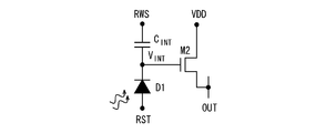
- FIG. 3A is an equivalent circuit diagram of the light detection sensor.
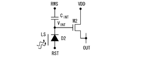
- FIG. 3B is an equivalent circuit diagram of the reference sensor.
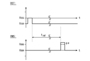
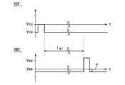
- FIG. 4 is a timing chart showing the waveforms of the reset signal supplied from the reset signal line RST and the read signal supplied from the read signal line RWS to the optical sensor in the display device according to the first embodiment of the present invention. is there.
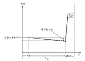
- FIG. 5 is a waveform diagram showing the relationship between the input signal (reset signal, readout signal) and V INT in the photosensor of the first embodiment.
- FIG. 1 is a block diagram showing a schematic configuration of a display device according to an embodiment of the present invention.
- FIG. 2 is an equivalent circuit diagram showing a configuration of one pixel in the display device according to the first embodiment of the present invention.
- FIG. 6 is a block diagram illustrating a schematic configuration of a compensation circuit included in the display device of the first embodiment.
- FIG. 7 is a waveform diagram showing an example of a read signal after being adjusted by the compensation circuit.
- FIG. 8 shows a high level V RWS. When the potential of H is V DD , the potential change of V INT (broken line) and the read signal high level V RWS. It is a signal waveform diagram showing the potential change (solid line) of V INT when the potential of H is (V DD + ⁇ ).
- FIG. 9 is a waveform diagram showing another example of the read signal after being adjusted by the compensation circuit.
- FIG. 10 is a timing chart showing sensor drive timings in the display device according to the first embodiment.
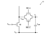
- FIG. 11 is a circuit diagram showing the internal configuration of the sensor pixel readout circuit.
- FIG. 12 is a waveform diagram showing the relationship among the readout signal, the sensor output, and the output of the sensor pixel readout circuit.
- FIG. 13 is a circuit diagram illustrating a configuration example of the sensor column amplifier.
- FIG. 14 is an equivalent circuit diagram of the photodetection sensor according to the second embodiment.
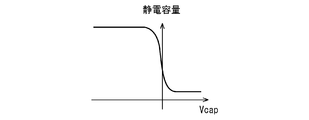
- FIG. 15 is a CV characteristic diagram of the variable capacitor C INT included in the photosensor according to the second embodiment.
- FIG. 16 is a waveform diagram showing the relationship between the input signal (reset signal, readout signal) and V INT in the photosensor according to the second embodiment.
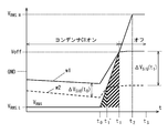
- FIG. 17 is a waveform diagram showing a change in the potential V INT of the storage node from the end of the integration period to the reading period.
- FIG. 18A is a schematic cross-sectional view showing the movement of charges when the potential of the gate electrode is lower than the threshold voltage in the variable capacitor.
- FIG. 18B is a schematic cross-sectional view showing the movement of charges when the potential of the gate electrode is higher than the threshold voltage in the variable capacitor.
- FIG. 19 is a block diagram illustrating a schematic configuration of a compensation circuit according to the second embodiment. 20 shows the potential change (broken line) of V INT before correction by the compensation circuit 70 and the low level V RWS. It is a signal waveform diagram showing the potential change (solid line) of V INT when the potential of L is lowered by ⁇ .
- FIG. 21 is a block diagram illustrating a schematic configuration of a compensation circuit according to the third embodiment.
- FIG. 22 is a waveform diagram showing an example of the reset signal after being adjusted by the compensation circuit of the third embodiment.
- FIG. 23 shows a high level V RST. When the potential of H is V SS , the potential change of V INT (broken line) and the high level V RST. It is a signal waveform diagram showing the potential change (solid line) of V INT when the potential of H is (V SS + ⁇ ).
- FIG. 24 is an equivalent circuit diagram showing a configuration of one pixel in a display device according to a modification of the third embodiment.
- FIG. 25 is a timing chart showing the waveforms of the reset signal supplied from the reset signal line RST and the read signal supplied from the read signal line RWS to the optical sensor in the display device according to the modification of the third embodiment. is there.
- FIG. 26 is a waveform diagram showing changes in V INT in the display device according to the modification of the third embodiment.
- FIG. 27 is an equivalent circuit diagram showing a configuration of one pixel in the display device according to the fourth embodiment.
- FIG. 28 is a block diagram illustrating a schematic configuration of a compensation circuit according to the fourth embodiment.
- FIG. 29 is a signal showing the potential change of V INT before the reset level potential V REF is adjusted (broken line) and the potential change of V INT after the reset level potential V REF is adjusted higher by ⁇ (solid line).
- FIG. 30 is an equivalent circuit diagram illustrating a configuration of one pixel in the display device according to the fifth embodiment.
- FIG. 31 is a signal showing the potential change of V INT before the reset level potential V REF is adjusted (broken line) and the potential change of V INT after the reset level potential V REF is adjusted higher by ⁇ (solid line). It is a waveform diagram.
- a display device is a display device including an optical sensor in a pixel region of an active matrix substrate, and the optical sensor outputs a sensor signal corresponding to the amount of received light;
- a reference sensor that outputs a sensor signal corresponding to an offset component, and has a configuration in which a light shielding film is added to the light detection sensor, and the display device includes a sensor signal output from the reference sensor,
- An offset comparison circuit that obtains a deviation degree from a standard offset value, and a drive signal generation circuit that adjusts the potential of the drive signal of the photosensor according to the deviation degree obtained by the offset comparison circuit.
- the optical sensor is connected between a light receiving element, a capacitor that charges and discharges an output current from the light receiving element, and one end of the light receiving element and one end of the capacitor.
- the generation circuit adjusts at least one of a high level potential and a low level potential of the read signal.
- the optical sensor includes a light receiving element, a variable capacitor that charges and discharges an output current from the light receiving element, and one end of the light receiving element and one end of the capacitor.
- the driving device comprising: a connected switching element; a reset signal line connected to the other end of the light receiving element for supplying a reset signal; and a read signal line connected to the other end of the capacitor for supplying a read signal.
- the signal generation circuit adjusts the low level potential of the read signal.
- the optical sensor is connected between a light receiving element, a capacitor that charges and discharges an output current from the light receiving element, and one end of the light receiving element and one end of the capacitor.
- a switching signal, a reset signal wiring connected to the other end of the light receiving element and supplying a reset signal, and a readout signal wiring supplying a readout signal to the photosensor, and the drive signal generation circuit includes The high-level potential of the reset signal is adjusted.
- the fifth configuration is a configuration in which, in the fourth configuration, the switching circuit includes one transistor, and the read signal wiring is connected to the other end of the capacitor.
- the switching circuit includes a first transistor and a second transistor, and the control electrode of the first transistor is one end of the light receiving element and one end of the capacitor. And one of two electrodes other than the control electrode in the first transistor is connected to a wiring for supplying a constant voltage, and two electrodes other than the control electrode in the first transistor are connected to each other.
- the other is connected to one of the two electrodes other than the control electrode in the second transistor, the other of the two electrodes other than the control electrode in the second transistor is connected to the output wiring of the sensor signal, and
- the readout signal wiring is connected to the control electrode of the second transistor, and the other end of the capacitor is connected to the wiring for supplying a constant voltage.
- the switching circuit includes a first transistor, a second transistor, and a third transistor, and the control electrode of the first transistor is one end of the light receiving element. And one end of two electrodes other than the control electrode in the first transistor are connected to a wiring for supplying a constant voltage, and other than the control electrode in the first transistor The other of the two electrodes is connected to one of the two electrodes other than the control electrode in the second transistor, and the other of the two electrodes other than the control electrode in the second transistor is connected to the output wiring of the sensor signal.
- the other end of the capacitor is connected to a wiring for supplying a constant voltage
- the readout signal wiring is connected to the control electrode of the second transistor
- the reset signal wiring is connected to the control electrode of the third transistor, one of the two electrodes other than the control electrode of the third transistor is connected to one end of the light receiving element, and the third transistor
- the other of the two electrodes other than the control electrode of the transistor is connected to a wiring for supplying a reference voltage, and the drive signal generation circuit adjusts the potential of the reference voltage of the third transistor.
- the switching circuit includes a first transistor and a second transistor, and a control electrode of the first transistor includes one end of the light receiving element and one end of the capacitor.
- One of the two electrodes other than the control electrode in the first transistor is connected to a wiring for supplying a constant voltage, and the other of the two electrodes other than the control electrode in the first transistor Is connected to the output wiring of the sensor signal, the other end of the capacitor is connected to the readout signal wiring, the reset signal wiring is connected to the control electrode of the second transistor, and the second transistor
- One of the two electrodes other than the control electrode is connected to one end of the light receiving element, and the two electrodes other than the control electrode of the second transistor It is connected to the reference voltage to a wiring for supplying the drive signal generating circuit is configured to adjust at least one of the potential of high level and a low level of the read signal.
- the switching circuit includes a first transistor and a second transistor, and a control electrode of the first transistor includes one end of the light receiving element and one end of the capacitor.
- One of the two electrodes other than the control electrode in the first transistor is connected to a wiring for supplying a constant voltage
- the other of the two electrodes other than the control electrode in the first transistor Is connected to the output wiring of the sensor signal
- the other end of the capacitor is connected to the readout signal wiring
- the reset signal wiring is connected to the control electrode of the second transistor
- One of the two electrodes other than the control electrode is connected to one end of the light receiving element, and the two electrodes other than the control electrode of the second transistor It is connected to the reference voltage to a wiring for supplying the drive signal generation circuit is configured to adjust the potential of the reference voltage.
- a display device includes a counter substrate facing the active matrix substrate and a sandwich between the active matrix substrate and the counter substrate in any of the first to ninth configurations. It is preferable that the liquid crystal display further includes a liquid crystal.
- the display device according to the present invention is implemented as a liquid crystal display device.
- the display device according to the present invention is not limited to the liquid crystal display device, and is an active matrix.
- the present invention can be applied to any display device using a substrate.
- the display device according to the present invention includes a touch panel display device that performs an input operation by detecting an object close to the screen by using an optical sensor, and a display for bidirectional communication including a display function and an imaging function. Use as a device is assumed.
- each drawing referred to below shows only the main members necessary for explaining the present invention in a simplified manner among the constituent members of the embodiment of the present invention for convenience of explanation. Therefore, the display device according to the present invention can include arbitrary constituent members that are not shown in the drawings referred to in this specification. Moreover, the dimension of the member in each figure does not represent the dimension of an actual structural member, the dimension ratio of each member, etc. faithfully.
- FIG. 1 is a block diagram showing a schematic configuration of an active matrix substrate 100 provided in a liquid crystal display device according to an embodiment of the present invention.
- an active matrix substrate 100 includes a pixel region 1, a display gate driver 2, a display source driver 3, a sensor column driver 4, a sensor row driver 5, and a buffer amplifier 6 on a glass substrate.
- FPC connector 7 is provided at least.
- a signal processing circuit 8 for processing an image signal captured by a light detection element (described later) in the pixel region 1 is connected to the active matrix substrate 100 via the FPC connector 7 and the FPC 9. .
- the above-described constituent members on the active matrix substrate 100 can be formed monolithically on the glass substrate by a semiconductor process. Or it is good also as a structure which mounted the amplifier and drivers among said structural members on the glass substrate by COG (Chip On Glass) technique etc., for example. Alternatively, it is conceivable that at least a part of the constituent members shown on the active matrix substrate 100 in FIG. 1 is mounted on the FPC 9.
- the active matrix substrate 100 is bonded to a counter substrate (not shown) having a counter electrode formed on the entire surface, and a liquid crystal material is sealed in the gap.
- the pixel area 1 is an area where a plurality of pixels are formed in order to display an image.
- an optical sensor for capturing an image is provided in each pixel in the pixel region 1.
- FIG. 2 is an equivalent circuit diagram showing the arrangement of pixels and photosensors in the pixel region 1 of the active matrix substrate 100.
- one pixel is formed by picture elements of three colors of R (red), G (green), and B (blue) (the picture elements are also called sub-pixels).
- One photosensor constituted by one photodiode (photodiode D1 in the example of FIG. 2), a capacitor CINT, and a thin film transistor M2 is provided in one pixel that is configured.
- the pixel region 1 includes pixels arranged in a matrix of M rows ⁇ N columns and photosensors arranged in a matrix of M rows ⁇ N columns. As described above, the number of picture elements is M ⁇ 3N.
- the pixel region 1 has gate lines GL and source lines COL arranged in a matrix as wiring for the pixels.
- the gate line GL is connected to the display gate driver 2.
- the source line COL is connected to the display source driver 3.
- the gate lines GL are provided in M rows in the pixel region 1.
- three source lines COL are provided for each pixel in order to supply image data to the three picture elements in one pixel.
- a thin film transistor (TFT) M1 is provided as a pixel switching element at the intersection of the gate line GL and the source line COL.
- the thin film transistor M1 provided in each of the red, green, and blue picture elements is denoted as M1r, M1g, and M1b.
- the thin film transistor M1 has a gate electrode connected to the gate line GL, a source electrode connected to the source line COL, and a drain electrode connected to a pixel electrode (not shown).
- a liquid crystal capacitor LC is formed between the drain electrode of the thin film transistor M1 and the counter electrode (VCOM).
- an auxiliary capacitor CLS is formed between the drain electrode and the TFTCOM.
- the pixel driven by the thin film transistor M1r connected to the intersection of one gate line GLi and one source line COLrj is provided with a red color filter corresponding to this pixel.
- red image data is supplied from the display source driver 3 via the source line COLrj, it functions as a red picture element.
- the pixel driven by the thin film transistor M1g connected to the intersection of the gate line GLi and the source line COLgj is provided with a green color filter so as to correspond to the picture element, and the display source is connected via the source line COLgj.
- green image data is supplied from the driver 3, it functions as a green picture element.
- the picture element driven by the thin film transistor M1b connected to the intersection of the gate line GLi and the source line COLbj is provided with a blue color filter so as to correspond to the picture element, and the display source is connected via the source line COLbj.
- blue image data is supplied from the driver 3, it functions as a blue picture element.
- one photosensor is provided for each pixel (three picture elements) in the pixel region 1.
- the arrangement ratio of the pixels and the photosensors is not limited to this example and is arbitrary.
- one photosensor may be arranged for each picture element, or one photosensor may be arranged for a plurality of pixels.
- the optical sensor includes a photodiode D1, a capacitor C INT, and a thin film transistor M2.
- a photodiode D1 for example, a lateral structure or a stacked structure PN junction or PIN junction diode can be used.
- the photosensor provided with the photodiode D1 functions as a photodetection sensor that outputs a sensor signal corresponding to the amount of received light.
- the display device has a configuration in which a light-shielding film is added to the light detection sensor in a part of pixels of the pixel region, and the reference sensor outputs a sensor signal corresponding to the offset component. It has.
- FIG. 3A is an equivalent circuit diagram of a light detection sensor provided with a photodiode D1.
- FIG. 3B is an equivalent circuit diagram of the reference sensor including the photodiode D2.
- the reference sensor has the same configuration as the photodetection sensor except that it includes a light shielding film LS.
- the photodetection sensor photodiode D1 and the reference sensor photodiode D2 are designed to have the same IV characteristics.
- the light shielding film LS needs to be provided so as to cover at least the light detection unit in the photodiode D2.
- the light shielding film LS may be provided so as to cover the entire circuit of the reference sensor or the entire pixel including the reference sensor.
- a reference sensor may be disposed on the peripheral pixel of the pixel region 1.
- a reference sensor may be arranged at a pixel at one end or both ends in the row direction or the column direction of the pixel region 1.
- the source line COLr also serves as the wiring VDD for supplying the constant voltage V DD from the sensor column driver 4 to the photosensor. Further, the source line COLg also serves as the sensor output wiring OUT.
- a reset signal line RST for supplying a reset signal is connected to the anode of the photodiode D1.
- the cathode of the photodiode D1 is connected between the gate of the thin film transistor M2 and one of the electrodes of the capacitor CINT .
- the drain of the thin film transistor M2 is connected to the wiring VDD, and the source is connected to the wiring OUT.
- the sensor row driver 5 sequentially selects a set of the reset signal wiring RSTi and the readout signal wiring RWSi shown in FIG. 2 at a predetermined time interval (t row ). As a result, the rows of photosensors from which signal charges are to be read out in the pixel region 1 are sequentially selected.
- the drain of a thin film transistor M3, which is an insulated gate field effect transistor, is connected to the end of the wiring OUT.
- An output wiring SOUT is connected to the drain of the thin film transistor M3, and the potential V SOUT of the drain of the thin film transistor M3 is output to the sensor column driver 4 as an output signal from the photosensor.
- the source of the thin film transistor M3 is connected to the wiring VSS.
- the gate of the thin film transistor M3 is connected to a reference voltage power source (not shown) via the reference voltage wiring VB.
- the light detection sensor including the photodiode D1 and the reference sensor including the photodiode D2 are different only in that the photodiode D2 does not receive external light.
- An operation example of the light detection sensor having the photodiode D1 will be described.
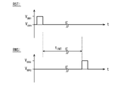
- FIG. 4 is a timing chart showing waveforms of a reset signal supplied from the reset signal wiring RST and a readout signal supplied from the readout signal wiring RWS to the optical sensor.
- FIG. 5 is a waveform diagram showing the relationship between the input signal (reset signal, readout signal) and V INT in the photosensor of the first embodiment.
- the high level V RST. H is a constant voltage V SSS (for example, 0 V), a low level V RST. L is a constant voltage V SSR (for example, ⁇ 4 V).
- the high level V RWS. H is a constant voltage V DDD (for example, 8 V), a low level V RWS. L is a constant voltage V DDR (for example, 0 V).
- the high level V RST. H (V SSS ) and the low level V RWS. L (V DDR ) was assumed to be the same potential (0 V). However, these voltage examples are merely examples, and the potential of each level can be set as appropriate.
- the photodiode D1 becomes a forward bias.
- the potential V INT of the gate electrode of the thin film transistor M2 is lower than the threshold voltage of the thin film transistor M2, the thin film transistor M2 is in a non-conductive state.
- the potential V INT at the connection point INT at the time of reset is expressed by the following equation (1).
- V INT V RST. H -V F (1)
- V RST. H is 0V is a high-level reset signal
- V F is the forward voltage of the photodiode D1. Since V INT at this time is lower than the threshold voltage of the transistor M2, the transistor M2 is non-conductive in the reset period.
- the reset signal is low level VRST.
- the photocurrent integration period (t INT ) begins.
- the light detecting sensor photodiode D1 is provided, the sum of the photocurrent I PHOTO dark current I DARK caused by the incident light flows out from the capacitor C INT, discharge capacitor C INT.
- the potential V INT at the connection point INT at the end of the integration period is expressed by the following equation (2).
- ⁇ V RST is the pulse amplitude (V RST.H -V RST.L ) of the reset signal
- C PD is the capacitance of the photodiode D1.
- C T is the total capacity of the connection point INT. That is, C T is equal to the sum of the capacitance C INT of the capacitor C INT , the capacitance C PD of the photodiode D1, and the capacitance C TFT of the transistor M2.
- V INT V RST. H ⁇ V F ⁇ V RST ⁇ C PD / C T -(I PHOTO + I DARK ) ⁇ t INT / C T (2)
- the component of the photocurrent I PHOTOTO is zero in the above equation (2), and only the dark current I DARK discharges the capacitor C INT . Note that also in the integration period, since V INT is lower than the threshold voltage of the transistor M2, the transistor M2 is non-conductive.
- V INT V RST. H ⁇ V F ⁇ (I PHOTO + I DARK ) ⁇ t INT / C T + ⁇ V RWS ⁇ C INT / C T (3)
- ⁇ V RWS is a pulse amplitude (V RWS.H ⁇ V RWS.L ) of the read signal. Accordingly, the potential V INT at the connection point INT becomes higher than the threshold voltage of the transistor M2. For this reason, the transistor M2 becomes conductive, and functions as a source follower amplifier together with the bias transistor M3 provided at the end of the wiring OUT in each column. That is, from the light detection sensor including the photodiode D1, as the output signal voltage Vout_D1 from the output wiring SOUT from the drain of the thin film transistor M3, the photocurrent I PHOTO and dark current due to the light incident on the photodiode D1 during the integration period A voltage obtained by amplifying the integral value of the sum with I DARK is obtained.
- a voltage obtained by amplifying the integrated value of the dark current I DARK in the integration period is obtained as the output signal voltage Vout_D2 from the output wiring SOUT from the drain of the thin film transistor M3.
- the waveform indicated by the solid line represents a change in the potential V INT in the photodetection sensor having the photodiode D ⁇ b> 1 when external light is incident.
- a waveform indicated by a broken line represents a change in the potential V INT in the reference sensor having the photodiode D2.
- the drop in the potential V INT from the reset level (0 V in the example of FIG. 5) corresponds to an offset component accompanying dark current or the like.
- the display device includes a compensation circuit 60 shown in FIG.
- the compensation circuit 60 is provided outside the active matrix substrate 100 (for example, in the signal processing circuit 8), but may be provided in the sensor row driver 5.
- the compensation circuit 60 includes an offset comparison circuit 61 and an RWS generation circuit 62 (drive signal generation circuit).
- the offset comparison circuit 61 compares the output signal voltage Vout_D2 from the reference optical sensor with a predetermined standard offset value to obtain the degree of divergence, and outputs a control signal corresponding to the obtained degree of divergence to the RWS generation circuit 62. Output to.
- the RWS generation circuit 62 controls the amplitude of the read signal (RWS) based on the control signal from the offset comparison circuit 61.
- the offset comparison circuit 61 uses a value obtained by A / D converting the output signal voltage Vout_D2 obtained from the reference photosensor when the ambient environment such as temperature and illuminance is set to a predetermined condition.
- the value is stored in the memory in advance, for example, before factory shipment.
- the sensor output characteristic with respect to the illuminance is linear (including 0 lux in which no light is incident).
- the offset comparison circuit 61 receives the output signal voltage Vout_D2 (output from the reference sensor) and performs A / D conversion on the output signal voltage Vout_D2 and the degree of deviation between the standard offset value and the standard offset value. Ask for.
- the offset comparison circuit 61 stores, for example, a function or a lookup table that outputs an adjustment value of the amplitude of the read signal as a control signal when the degree of deviation between the gradation data and the standard offset value is input. Has been. Using this function or table, the offset comparison circuit 61 outputs a control signal (adjustment value of the amplitude of the read signal) according to the degree of deviation between the gradation data of the output signal voltage Vout_D2 of the reference sensor and the standard offset value. To do.
- the adjustment of the amplitude of the read signal by the compensation circuit 60 may be performed for each frame, and there is no particular limitation on the execution timing, for example, at a predetermined time interval in addition to when the display device is activated.
- FIG. 7 is a waveform diagram showing an example of the read signal after being adjusted by the compensation circuit 60.
- the RWS generation circuit 62 generates a high level V RWS.
- the amplitude of the read signal (V RWS.H ⁇ V RWS.L ) is increased by ⁇ by increasing the potential of H by ⁇ with respect to V DDD before correction (see FIG. 4).
- This offset potential ⁇ is a value determined by the offset comparison circuit 61 according to the degree of deviation between the output signal voltage Vout_D2 of the reference sensor and the standard offset value.
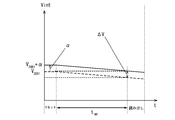
- FIG. 8 shows a high level V RWS.
- the potential change of V INT (broken line) and the read signal high level V RWS.
- It is a signal waveform diagram showing the potential change (solid line) of V INT when the potential of H is (V DDD + ⁇ ).
- the read signal high level V RWS By setting the potential of H to (V DDD + ⁇ ), the potential of V INT increases by a voltage ⁇ V corresponding to the offset ⁇ .
- the magnitude of the voltage ⁇ V is strictly ( ⁇ ⁇ C INT / C T ) according to the above equation (3).
- the high level V RWS Of the read signal according to the degree of deviation between the gradation data of the output signal voltage Vout_D2 and the standard offset value .
- the potential of H By setting the potential of H to (V DDD + ⁇ ), a signal in which the offset due to dark current or the like is eliminated can be obtained as the output signal voltage Vout_D1.
- the present embodiment there is no need to subtract the output of the reference sensor from the output of the light detection sensor as in the prior art, so that there is no problem that the dynamic range of the sensor output is narrowed.
- a display device that can detect the intensity of external light with high accuracy without being influenced by the environmental temperature and that includes a photosensor with a wide dynamic range.
- the read signal high level V RWS.
- the amplitude of the read signal was increased by ⁇ .
- the low level V RWS As shown in FIG. 9, the low level V RWS.
- the potential of L By changing the potential of L from V SSR to (V SSR - ⁇ ), the amplitude of the read signal can be increased by ⁇ , so the same effect can be obtained.
- the source lines COLr and COLg are shared as the optical sensor wirings VDD and OUT, as shown in FIG. 10, the source lines COLr, COLg, and COLb are connected via the source lines COLr, COLg, and COLb. It is necessary to distinguish the timing for inputting the image data signal for display from the timing for reading the sensor output.
- the sensor output is read using the horizontal blanking period or the like. That is, after the input of the display image data signal is finished, the constant voltage V DDD is applied to the source line COLr.
- HSYNC in FIG. 10 indicates a horizontal synchronization signal.
- the sensor column driver 4 includes a sensor pixel readout circuit 41, a sensor column amplifier 42, and a sensor column scanning circuit 43.
- An output wiring SOUT (see FIG. 2) that outputs the sensor output V SOUT from the pixel region 1 is connected to the sensor pixel readout circuit 41.
- the sensor pixel readout circuit 41 outputs the peak hold voltage V Sj of the sensor output V SOUTj to the sensor column amplifier 42.
- V COUT is output to the buffer amplifier 6.
- FIG. 11 is a circuit diagram showing the internal configuration of the sensor pixel readout circuit 41.
- FIG. 12 is a waveform diagram showing the relationship between the readout signal V RWS , the sensor output V SOUT, and the output V S of the sensor pixel readout circuit.
- the read signal is at the high level V RWS.
- a source follower amplifier is formed by the thin film transistors M2 and M3, and the sensor output V SOUT is accumulated in the sample capacitor C SAM of the sensor pixel readout circuit 41.
- the read signal is low level V RWS.
- the output voltage V S from the sensor pixel readout circuit 41 to the sensor column amplifier 42 is the peak value of the sensor output V SOUT as shown in FIG. Is held at a level equal to.
- each column amplifier includes thin film transistors M6 and M7.
- the buffer amplifier 6 further amplifies V COUT output from the sensor column amplifier 42 and outputs the amplified signal to the signal processing circuit 8 as a panel output (photosensor signal) V out .
- the sensor column scanning circuit 43 may scan the optical sensor columns one by one as described above, but is not limited thereto, and may be configured to interlace scan the optical sensor columns. Further, the sensor column scanning circuit 43 may be formed as a multi-phase driving scanning circuit such as a four-phase.
- the display device obtains a panel output VOUT corresponding to the amount of light received by the photodiode D1 formed for each pixel in the pixel region 1.
- the panel output VOUT is sent to the signal processing circuit 8, A / D converted, and stored in a memory (not shown) as panel output data. That is, the same number of panel output data as the number of pixels (number of photosensors) in the pixel region 1 is stored in this memory.
- the signal processing circuit 8 performs various signal processing such as image capture and touch area detection using the panel output data stored in the memory.
- the same number of panel output data as the number of pixels (number of photosensors) in the pixel region 1 is accumulated in the memory of the signal processing circuit 8.
- the number of pixels is not necessarily limited due to restrictions such as memory capacity. It is not necessary to store the same number of panel output data.
- the amplitude of the readout signal is adjusted according to the degree of deviation between the gradation data of the output signal voltage Vout_D2 and the standard offset value.
- the display device has the first feature in that a variable capacitor is used as the capacitance of the photosensor and that the compensation circuit 60 adjusts the low-level potential of the read signal instead of the amplitude of the read signal. This is different from the display device according to the embodiment.
- FIG. 14 is an equivalent circuit diagram of the photodetection sensor according to the second embodiment.
- the photodetection sensor according to the present embodiment is different from the photodetection sensor according to the first embodiment in that the capacitance C INT is a variable capacitance.
- the reference sensor according to the present embodiment also has the same variable capacitance as the photodetection sensor as the capacitance C INT .
- the variable capacitor for example, a p-channel MOS capacitor or an n-channel MOS capacitor can be used.
- FIG. 15 is a CV characteristic diagram of the variable capacitor C INT of this embodiment.
- the horizontal axis represents the interelectrode voltage V CAP of the variable capacitor C INT
- the vertical axis represents the capacitance.
- the variable capacitance C INT has a constant capacitance while the interelectrode voltage V CAP is small, but the capacitance changes sharply before and after the threshold value of the interelectrode voltage V CAP.
- the characteristics of the variable capacitor C INT can be dynamically changed by the potential of the read signal supplied from the wiring RWS.
- the photosensor according to the present embodiment can amplify and read out the potential change of the storage node in the integration period t INT as shown in FIG.
- FIG. 16 is merely a specific example, but the low level V RST. L is ⁇ 1.4V, and the reset signal high level V RST. H is 0V. Further, the low level V RWS. L is -3V, read signal high level V RWS. H is 12V. Also in FIG. 16, the waveform shown by the solid line represents the change in the potential V INT when the light incident on the photodiode D1 is small, and the waveform shown by the broken line is the case where the light of saturation level is incident on the photodiode D1. Represents a change in the potential V INT , and ⁇ V SIG is a potential difference proportional to the amount of light incident on the photodiode D1.
- the potential change of the accumulation node in the integration period t INT when the light of the saturation level is incident is relatively small, but in the readout period (the potential of the readout signal is at the high level V RWS.H. During this period, the potential V INT of this storage node is amplified and read out.
- FIG. 17 is a waveform diagram showing a change in the potential V INT of the storage node from the end of the integration period to the reading period.
- a waveform w1 indicated by a solid line represents a change in the potential V INT when light is incident on the photodiode D1
- a waveform w2 indicated by a broken line is a potential when light is incident on the photodiode D1. It represents a change in V INT .
- the read signal supplied from the wiring RWS is low level V RWS.
- Time t 2 is the time when the transistor M2 is turned on and the sensor output is sampled.
- Time t 1 is the time when the read signal reaches the threshold voltage V off of the variable capacitance C INT.
- Time t 1 ′ is the time when the read signal reaches the threshold voltage V off of the variable capacitor C INT when light is incident on the photodiode D1 (in the case of the waveform w2). That is, the operating characteristics of the variable capacitor C INT vary depending on the magnitude relationship between the potential supplied from the read wiring RWS and the threshold voltage V off .
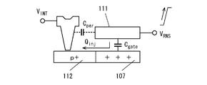
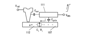
- 18A and 18B are schematic cross-sectional views showing the difference in charge transfer according to the potential of the gate electrode in the variable capacitor C INT when the variable capacitor C INT is formed of a p-channel MOS capacitor.
- the variable capacitor C INT includes a gate electrode 111, an n ⁇ region 107 formed in the silicon film, and an insulating film (not shown) provided therebetween.
- 18A and 18B is a p + region formed by doping an n-type silicon film with a p-type impurity such as boron.
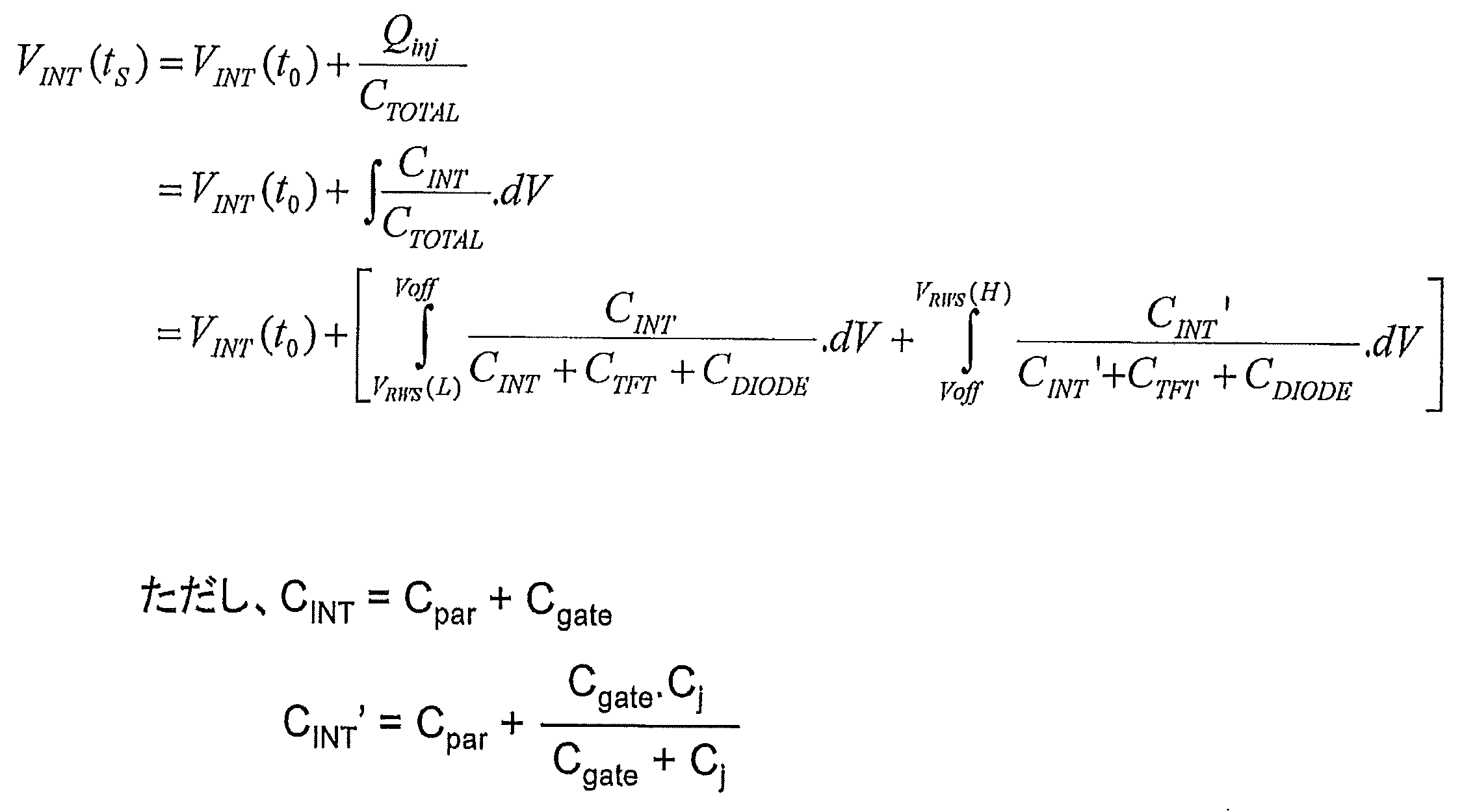
- the variable capacitance C INT is always on, after time t 1 is turned off. That is, while the potential of the wiring RWS is equal to or lower than the threshold voltage V off , the charge Q inj below the gate electrode 111 moves as shown in FIG. 18A. On the other hand, when the potential of the wiring RWS exceeds the threshold voltage V off , the charge Q inj under the gate electrode 111 does not move as shown in FIG. 18B.
- the potential of the read signal supplied from the read wiring RWS is high level V RWS.
- the potential V INT (t s ) of the storage node at the sample time t s after reaching H is as shown in the following equation. Note that ⁇ V INT shown in FIG. 16 corresponds to the difference between V INT (t 0 ) and V INT (t s ), and is equal to Q inj / C INT .
- ⁇ V SIG (t 0 ) at the end of the integration period is amplified to ⁇ V SIG (t 1 ).
- the potential difference after the push-up becomes larger than the potential difference of the storage node due to the difference in illuminance on the light receiving surface at the end of the integration period.
- the readout period in the dark state is greater than the potential difference between the potential of the storage node at the end of the integration period in the dark state and the potential of the storage node at the end of the integration period in the case where light of saturation level is incident.
- the reference sensor since it is shielded so as not to receive external light, only a dark current component due to temperature change, ambient light (backlight light, etc.) or a change with time is detected. .
- FIG. 19 is a block diagram showing a schematic configuration of the compensation circuit 70 according to the present embodiment.
- the compensation circuit 70 is provided outside the active matrix substrate 100 (for example, in the signal processing circuit 8), but may be provided in the sensor row driver 5.
- the compensation circuit 70 includes an offset comparison circuit 61 and an RWS_L generation circuit 72.
- the offset comparison circuit 61 compares the output signal voltage Vout_D2 from the reference optical sensor with a predetermined standard offset value to obtain the degree of deviation, and outputs a control signal corresponding to the obtained degree of deviation to the RWS_L generation circuit 72. Output to.
- the RWS_L generation circuit 72 controls the low-level potential (V RWS.L ) of the read signal (RWS) based on the control signal from the offset comparison circuit 61. Specifically, according to the degree of deviation between the output signal Vout_D2 of the reference sensor and the standard offset value, V RWS. Lower the potential of L by ⁇ . That is, the offset potential ⁇ is a value determined by the offset comparison circuit 61 according to the degree of deviation between the output signal Vout_D2 of the reference sensor and the standard offset value.
- V INT shows the potential change (broken line) of V INT before correction by the compensation circuit 70 and the low level V RWS. It is a signal waveform diagram showing the potential change (solid line) of V INT when the potential of L is lowered by ⁇ . As shown in FIG. 20, the low level V RWS. By reducing the potential of L by ⁇ , the potential of V INT increases by a voltage ⁇ V corresponding to the offset ⁇ .
- the low-level potential of the read signal is adjusted according to the degree of deviation between the gradation data of the output signal voltage Vout_D2 and the standard offset value.
- the configuration of the light sensor (the light detection sensor and the reference sensor) is the same as that of the first embodiment.
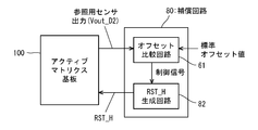
- the display device according to the present embodiment differs from the first embodiment in the configuration of the compensation circuit. That is, instead of the compensation circuit 60 that adjusts the amplitude of the read signal disclosed in the first embodiment, the display device according to this embodiment includes a compensation circuit 80 that adjusts the high-level potential of the reset signal. Yes.
- FIG. 21 is a block diagram showing a schematic configuration of the compensation circuit 80 of the present embodiment.
- the compensation circuit 80 is provided outside the active matrix substrate 100 (for example, in the signal processing circuit 8), but may be provided in the sensor row driver 5.
- the compensation circuit 80 includes an offset comparison circuit 61 and an RST_H generation circuit 82.
- the offset comparison circuit 61 compares the output signal voltage Vout_D2 from the reference photosensor with a predetermined standard offset value to obtain the degree of divergence, and generates a control signal corresponding to the obtained degree of divergence RST_H generation circuit 82. Output to.
- the RST_H generation circuit 82 adjusts the high-level potential (V RST.H ) of the reset signal based on the control signal from the offset comparison circuit 61.
- FIG. 22 is a waveform diagram showing an example of the read signal after being adjusted by the compensation circuit 80.
- the RST_H generation circuit 82 generates a high-level potential V RST. H is increased by ⁇ relative to V SSS before correction (see FIG. 4).
- This offset potential ⁇ is a value determined by the offset comparison circuit 61 according to the degree of deviation between the output signal voltage Vout_D2 of the reference sensor and the standard offset value.
- FIG. 23 shows a high level V RST.
- the potential change of V INT (broken line) and the high level V RST.
- It is a signal waveform diagram showing the potential change (solid line) of V INT when the potential of H is (V SSS + ⁇ ).
- the high-level potential V RST By setting H to (V SSS + ⁇ ), the potential of V INT increases by a voltage ⁇ V corresponding to the offset ⁇ .
- the high level V RST As described above, the high level V RST. Of the reset signal according to the degree of deviation between the gradation data of the output signal voltage Vout_D2 and the standard offset value .
- the potential of H By setting the potential of H to (V SSS + ⁇ ), as the output signal voltage Vout_D1, a signal in which the offset due to dark current or the like is eliminated can be obtained.
- FIG. 24 is an equivalent circuit diagram illustrating a configuration of one pixel in the display device according to the first modification of the third embodiment.
- the optical sensor of the display device according to the first modification further includes a thin film transistor M4 in addition to the photodiode D1, the capacitor C INT , and the thin film transistor M2.
- a part of the pixels in the pixel region 1 includes a reference sensor provided with a photodiode D2 including a light shielding film LS instead of the photodiode D1. It is.
- one electrode of the capacitor C INT is connected between the gate electrode of the cathode and the thin film transistor M2 of the photodiode D1, and the other electrode of the capacitor C INT, connected to the wiring VDD Has been.
- the drain of the thin film transistor M2 is connected to the wiring VDD, and the source is connected to the drain of the thin film transistor M4.
- the gate of the thin film transistor M4 is connected to the read signal wiring RWS.
- the source of the thin film transistor M4 is connected to the wiring OUT.
- one of the electrodes of the capacitor C INT and the drain of the thin film transistor M2 are connected to a common constant voltage wiring (wiring VDD). However, they are connected to different constant voltage wirings. It may be a connected configuration.
- FIG. 25 the operation of the optical sensor according to the first modification will be described with reference to FIGS. 25 and 26.
- FIG. 25 is a timing chart showing waveforms of a reset signal supplied from the reset signal line RST to the optical sensor and a read signal supplied from the read signal line RWS.
- FIG. 26 is a waveform diagram showing changes in V INT during the reset period, the integration period, and the readout period in the optical sensor of the first modification.
- a broken line indicates a change in V INT before correcting the high-level potential of the reset signal
- a solid line indicates a change in V INT after correction.
- High level of reset signal VRST. H is set to a potential at which the thin film transistor M2 is turned on.
- the high level V RST. H is equal to V DDD1
- the low level V RST. L is equal to V DDR1
- the high level V RWS. H is equal to V DDD2
- the low level V RWS. L is equal to V DDR2 .
- these voltage examples are merely examples, and the potential of each level can be set as appropriate.
- the photodiode D1 becomes a forward bias.
- the thin film transistor M2 is turned on, but since the read signal is at a low level and the thin film transistor M4 is turned off, there is no output to the wiring OUT.
- the reset signal is low level VRST.
- the photocurrent integration period (period t INT shown in FIGS. 25 and 26) starts.
- the current by the photodiode flows out from the capacitor C INT, discharge capacitor C INT.
- the sum of the photocurrent I PHOTO and dark current I DARK generated by the incident light flows out from the capacitor C INT .
- the dark current I DARK flows out from the capacitor C INT .
- V INT falls from the reset potential according to the intensity of incident light.
- the thin film transistor M4 since the thin film transistor M4 is in an off state, there is no sensor output to the wiring OUT. It should be noted that when the photodiode D1 is irradiated with light having an upper limit of illuminance to be detected, the sensor output is minimized, that is, in this case, the potential (V INT ) of the gate electrode of the thin film transistor M2 slightly decreases the threshold value. It is desirable to design the sensor circuit so as to exceed the value.
- the read signal rises to start the read period.
- the thin film transistor M4 is turned on. Accordingly, an output from the thin film transistor M2 is output to the wiring OUT through the thin film transistor M4.
- the thin film transistor M2 functions as a source follower amplifier together with the bias thin film transistor M3 provided at the end of the wiring OUT in each column.
- the compensation circuit 80 offsets the high-level potential of the reset signal based on the output signal voltage Vout_D2 from the reference sensor including the photodiode D2. Is adjusted to be higher by the amount corresponding to ( ⁇ ). That is, as shown in FIG. 26, the high level potential V RST. By setting H to (V DDD1 + ⁇ ), the potential of V INT increases by a voltage ⁇ V corresponding to the offset ⁇ .
- the high level V RST Of the reset signal according to the degree of deviation between the gradation data of the output signal voltage Vout_D2 and the standard offset value .
- the potential of H By setting the potential of H to (V DDD1 + ⁇ ), a signal in which the offset due to dark current or the like is eliminated can be obtained as the output signal voltage Vout_D1.
- FIG. 27 is an equivalent circuit diagram showing a configuration of one pixel in the display device according to the fourth embodiment.
- the optical sensor of the display device according to the modification 2 further includes thin film transistors M4 and M5 in addition to the photodiode D1, the capacitor C INT and the thin film transistor M2. Note that, in some pixels of the pixel region 1, a reference sensor having a photodiode D2 having a light-shielding film LS is provided instead of the light detection sensor having the photodiode D1. This is the same as the embodiment.
- one electrode of the capacitor C INT is connected between the cathode of the photodiode D1 and the gate of the thin film transistor M2.
- the other electrode of the capacitor C INT is connected to GND.
- the drain of the thin film transistor M2 is connected to the wiring VDD, and the source is connected to the drain of the thin film transistor M4.
- the gate of the thin film transistor M4 is connected to the read signal wiring RWS.
- the source of the thin film transistor M4 is connected to the wiring OUT.
- the thin film transistor M5 has a gate connected to the reset signal line RST, a drain connected to the line REF, and a source connected to the cathode of the photodiode D1.
- the wiring REF supplies a reset level potential VREF .
- FIG. 29 is a waveform diagram showing changes in V INT during the reset period, the integration period, and the readout period in the photosensor of the present embodiment.
- a broken line indicates a change in V INT before correcting the reset level potential V REF
- a solid line indicates a change in V INT after correction.
- High level of reset signal VRST. H is set to a potential at which the thin film transistor M5 is turned on.
- the high level V RST. H is equal to V DDD1
- the low level V RST. L is equal to V DDR1
- the high level V RWS. H is equal to V DDD2
- the low level V RWS. L is equal to V DDR2 .
- these voltage examples are merely examples, and the potential of each level can be set as appropriate.
- the reset signal is low level VRST.
- the photocurrent integration period begins.
- the thin film transistor M5 is turned off.
- a reverse bias is applied to the photodiode D1.
- the current by the photodiode D1 flows out from the capacitor C INT, discharge capacitor C INT.
- the photodetection sensor provided with the photodiode D1 the sum of the photocurrent I PHOTO and dark current I DARK generated by the incident light flows out from the capacitor C INT .
- the dark current I DARK flows out from the capacitor C INT .
- the thin film transistor M4 since the thin film transistor M4 is in an off state, there is no sensor output to the wiring OUT.
- the sensor output is minimized, that is, in this case, the potential (V INT ) of the gate electrode of the thin film transistor M2 slightly decreases the threshold value.
- the read signal rises to start the read period.
- the thin film transistor M4 is turned on. Accordingly, an output from the thin film transistor M2 is output to the wiring OUT through the thin film transistor M4.
- the thin film transistor M2 functions as a source follower amplifier together with the bias thin film transistor M3 provided at the end of the wiring OUT in each column.
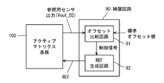
- FIG. 28 is a block diagram illustrating a schematic configuration of a compensation circuit 90 included in the display device according to the fourth embodiment.
- the compensation circuit 90 is provided outside the active matrix substrate 100 (for example, in the signal processing circuit 8), but may be provided in the sensor row driver 5.
- the compensation circuit 90 includes an offset comparison circuit 61 and a REF generation circuit 92.
- the offset comparison circuit 61 compares the output signal voltage Vout_D2 from the reference optical sensor with a predetermined standard offset value to obtain the degree of deviation, and generates a control signal corresponding to the obtained degree of deviation from the REF generation circuit 92. Output to.
- the REF generation circuit 92 adjusts the reset level potential V REF supplied from the wiring REF based on the control signal from the offset comparison circuit 61. That is, the REF generation circuit 92 sets the reset level potential V REF higher by an amount ( ⁇ ) corresponding to the offset.
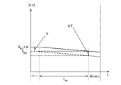
- FIG. 29 is a signal showing the potential change of V INT before the reset level potential V REF is adjusted (broken line) and the potential change of V INT after the reset level potential V REF is adjusted higher by ⁇ (solid line). It is a waveform diagram. As shown in FIG. 29, by setting the reset level potential V REF higher by ⁇ , the potential of V INT increases by a voltage ⁇ V corresponding to the offset ⁇ .
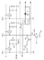
- FIG. 30 is an equivalent circuit diagram illustrating a configuration of one pixel in the display device according to the fifth embodiment.
- the optical sensor of the display device according to this embodiment further includes a thin film transistor M5 in addition to the photodiode D1, the capacitor C INT , and the thin film transistor M2.
- a reference sensor having a photodiode D2 having a light-shielding film LS is provided instead of the light detection sensor having the photodiode D1. This is the same as the embodiment.
- one electrode of the capacitor C INT is connected between the cathode of the photodiode D1 and the gate of the thin film transistor M2.
- the other electrode of the capacitor C INT is connected to the read signal wiring RWS.
- the drain of the thin film transistor M2 is connected to the wiring VDD, and the source is connected to the wiring OUT.
- the thin film transistor M5 has a gate connected to the reset signal line RST, a drain connected to the line REF, and a source connected to the cathode of the photodiode D1.
- the wiring REF supplies a reset level potential VREF .
- the anode of the photodiode D1 is connected to a COM that supplies a constant voltage.
- the waveforms of the reset signal supplied from the reset signal wiring RST and the readout signal supplied from the readout signal wiring RWS are the same as those in FIG. 4 referred to in the first embodiment.
- the display device according to the present embodiment includes a compensation circuit 60 shown in FIG. 6 referred to in the first embodiment. Similar to the first embodiment, the compensation circuit 60 can be provided outside the active matrix substrate 100 (for example, in the signal processing circuit 8) or in the sensor row driver 5.
- the compensation circuit 60 reads out according to the degree of deviation between the value (grayscale data) obtained by A / D converting the output signal voltage Vout_D2 from the reference sensor and the standard offset value. Adjust the amplitude of the signal. That is, the RWS generation circuit 62 of the compensation circuit 60 performs the high level V RWS. Of the read signal as described with reference to FIG. 7 in the first embodiment .
- the amplitude of the read signal (V RWS.H ⁇ V RWS.L ) is increased by ⁇ by increasing the potential of H by ⁇ with respect to V DDD before correction (see FIG. 4).
- the high level V RWS By setting the potential of H to (V DDD + ⁇ ), the potential of V INT increases by a voltage ⁇ V corresponding to the offset ⁇ .
- the high level V RWS Of the read signal according to the degree of deviation between the gradation data of the output signal voltage Vout_D2 and the standard offset value .
- the potential of H By setting the potential of H to (V DDD + ⁇ ), a signal in which the offset due to dark current or the like is eliminated can be obtained as the output signal voltage Vout_D1.
- the high level V RWS By changing the potential of H from V DDD to (V DDD + ⁇ ), the amplitude of the read signal was increased by ⁇ .
- the low level V RWS By changing the potential of L from V SSR to (V SSR - ⁇ ), the amplitude of the read signal can be increased by ⁇ , so the same effect can be obtained.
- the reset level potential V REF may be adjusted instead of the amplitude of the read signal in accordance with the degree of deviation between the gradation data of the output signal voltage Vout_D2 and the standard offset value. good.
- a compensation circuit 90 shown in FIG. 28 referred to in the fourth embodiment is provided instead of the compensation circuit 60. If the reset level potential V REF is set higher by ⁇ by providing the compensation circuit 90, the potential of V INT at the time of reset rises by a voltage corresponding to the offset ⁇ as shown in FIG. Thereby, at the time of reading, a value with offset canceled is output.
- the solid line represents the potential change of V INT before correction of the reset level potential V REF , and the broken line represents the potential change of V INT after correction.
- the configuration in which the wirings VDD and OUT connected to the optical sensor are shared with the source wiring COL is exemplified. According to this configuration, there is an advantage that the pixel aperture ratio is high. However, the same effects as those of the above-described embodiments can be obtained also by a configuration in which the optical sensor wirings VDD and OUT are provided separately from the source wiring COL.
- the present invention is industrially applicable as a display device having an optical sensor function.
Landscapes
- Engineering & Computer Science (AREA)
- General Engineering & Computer Science (AREA)
- Theoretical Computer Science (AREA)
- Human Computer Interaction (AREA)
- Physics & Mathematics (AREA)
- General Physics & Mathematics (AREA)
- Control Of Indicators Other Than Cathode Ray Tubes (AREA)
- Liquid Crystal (AREA)
- Position Input By Displaying (AREA)
Abstract
Description
[実施の形態]
最初に、図1および図2を参照しながら、本発明の第1の実施形態にかかる液晶表示装置が備えるアクティブマトリクス基板の構成について説明する。
-(IPHOTO+IDARK)・tINT/CT …(2)
+ΔVRWS・CINT/CT …(3)
[第2の実施形態]
[第3の実施形態]
[第3の実施形態の変形例1]
[第4の実施形態]
[第5の実施形態]
[第1~第5の実施形態についての変形例]
Claims (10)
- アクティブマトリクス基板の画素領域に光センサを備えた表示装置であって、
前記光センサが、受光量に応じたセンサ信号を出力する光検出用センサと、前記光検出用センサに遮光膜が追加された構成を有しオフセット成分に応じたセンサ信号を出力する参照用センサとを含み、
前記表示装置は、
前記参照用センサから出力されたセンサ信号と標準オフセット値との乖離度合いを求めるオフセット比較回路と、
前記オフセット比較回路で求められた前記乖離度合いに応じて前記光センサの駆動信号の電位を調整する駆動信号生成回路とを備えた、表示装置。 - 前記光センサが、
受光素子と、
前記受光素子からの出力電流を充放電する容量と、
前記受光素子の一端と前記容量の一端との間に接続されたスイッチング素子と、
当該受光素子の他端に接続され、リセット信号を供給するリセット信号配線と、
当該容量の他端に接続され、読み出し信号を供給する読み出し信号配線とを備え、
前記駆動信号生成回路が、前記読み出し信号のハイレベルおよびローレベルの少なくとも一方の電位を調整する、請求項1に記載の表示装置。 - 前記光センサが、
受光素子と、
前記受光素子からの出力電流を充放電する可変容量と、
前記受光素子の一端と前記容量の一端との間に接続されたスイッチング素子と、
当該受光素子の他端に接続され、リセット信号を供給するリセット信号配線と、
当該容量の他端に接続され、読み出し信号を供給する読み出し信号配線とを備え、
前記駆動信号生成回路が、前記読み出し信号のローレベルの電位を調整する、請求項1に記載の表示装置。 - 前記光センサが、
受光素子と、
前記受光素子からの出力電流を充放電する容量と、
前記受光素子の一端と前記容量の一端との間に接続されたスイッチング回路と、
当該受光素子の他端に接続され、リセット信号を供給するリセット信号配線と、
前記光センサへ読み出し信号を供給する読み出し信号配線とを備え、
前記駆動信号生成回路が、前記リセット信号のハイレベルの電位を調整する、請求項1に記載の表示装置。 - 前記スイッチング回路が、1つのトランジスタを備え、
前記読み出し信号配線が、前記容量の他端に接続されている、請求項4に記載の表示装置。 - 前記スイッチング回路が、第1のトランジスタおよび第2のトランジスタを備え、
前記第1のトランジスタの制御電極が、前記受光素子の一端と前記容量の一端との間に接続され、
前記第1のトランジスタにおける前記制御電極以外の2つの電極の一方が、定電圧を供給する配線に接続され、
前記第1のトランジスタにおける前記制御電極以外の2つの電極の他方が、第2のトランジスタにおける制御電極以外の2つの電極の一方に接続され、
前記第2のトランジスタにおける制御電極以外の2つの電極の他方が、前記センサ信号の出力配線に接続され、
前記第2のトランジスタの制御電極に、前記読み出し信号配線が接続され、
前記容量の他端が、定電圧を供給する配線に接続された、請求項4に記載の表示装置。 - 前記スイッチング回路が、第1のトランジスタ、第2のトランジスタ、および第3のトランジスタを備え、
前記第1のトランジスタの制御電極が、前記受光素子の一端と前記容量の一端との間に接続され、
前記第1のトランジスタにおける前記制御電極以外の2つの電極の一方が、定電圧を供給する配線に接続され、
前記第1のトランジスタにおける前記制御電極以外の2つの電極の他方が、第2のトランジスタにおける制御電極以外の2つの電極の一方に接続され、
前記第2のトランジスタにおける制御電極以外の2つの電極の他方が、前記センサ信号の出力配線に接続され、
前記容量の他端が定電圧を供給する配線に接続され、
前記第2のトランジスタの制御電極に、前記読み出し信号配線が接続され、
前記第3のトランジスタの制御電極に、前記リセット信号配線が接続され、
前記第3のトランジスタの前記制御電極以外の2つの電極の一方が、前記受光素子の一端に接続され、
前記第3のトランジスタの前記制御電極以外の2つの電極の他方が、参照電圧を供給する配線に接続され、
前記駆動信号生成回路が、前記第3のトランジスタの前記参照電圧の電位を調整する、請求項1に記載の表示装置。 - 前記スイッチング回路が、第1のトランジスタおよび第2のトランジスタを備え、
前記第1のトランジスタの制御電極が、前記受光素子の一端と前記容量の一端との間に接続され、
前記第1のトランジスタにおける前記制御電極以外の2つの電極の一方が、定電圧を供給する配線に接続され、
前記第1のトランジスタにおける前記制御電極以外の2つの電極の他方が、前記センサ信号の出力配線に接続され、
前記容量の他端が、前記読み出し信号配線に接続され、
前記第2のトランジスタの制御電極に、前記リセット信号配線が接続され、
前記第2のトランジスタの前記制御電極以外の2つの電極の一方が、前記受光素子の一端に接続され、
前記第2のトランジスタの前記制御電極以外の2つの電極の他方が、参照電圧を供給する配線に接続され、
前記駆動信号生成回路が、前記読み出し信号のハイレベルおよびローレベルの少なくとも一方の電位を調整する、請求項1に記載の表示装置。 - 前記スイッチング回路が、第1のトランジスタおよび第2のトランジスタを備え、
前記第1のトランジスタの制御電極が、前記受光素子の一端と前記容量の一端との間に接続され、
前記第1のトランジスタにおける前記制御電極以外の2つの電極の一方が、定電圧を供給する配線に接続され、
前記第1のトランジスタにおける前記制御電極以外の2つの電極の他方が、前記センサ信号の出力配線に接続され、
前記容量の他端が、前記読み出し信号配線に接続され、
前記第2のトランジスタの制御電極に、前記リセット信号配線が接続され、
前記第2のトランジスタの前記制御電極以外の2つの電極の一方が、前記受光素子の一端に接続され、
前記第2のトランジスタの前記制御電極以外の2つの電極の他方が、参照電圧を供給する配線に接続され、
前記駆動信号生成回路が前記参照電圧の電位を調整する、請求項1に記載の表示装置。 - 前記アクティブマトリクス基板に対向する対向基板と、
前記アクティブマトリクス基板と対向基板との間に挟持された液晶とをさらに備えた、請求項1~9のいずれか一項に記載の表示装置。
Priority Applications (2)
| Application Number | Priority Date | Filing Date | Title |
|---|---|---|---|
| JP2012515926A JPWO2011145682A1 (ja) | 2010-05-20 | 2011-05-19 | 表示装置 |
| US13/697,864 US20130057527A1 (en) | 2010-05-20 | 2011-05-19 | Display device |
Applications Claiming Priority (2)
| Application Number | Priority Date | Filing Date | Title |
|---|---|---|---|
| JP2010116445 | 2010-05-20 | ||
| JP2010-116445 | 2010-05-20 |
Publications (1)
| Publication Number | Publication Date |
|---|---|
| WO2011145682A1 true WO2011145682A1 (ja) | 2011-11-24 |
Family
ID=44991774
Family Applications (1)
| Application Number | Title | Priority Date | Filing Date |
|---|---|---|---|
| PCT/JP2011/061524 Ceased WO2011145682A1 (ja) | 2010-05-20 | 2011-05-19 | 表示装置 |
Country Status (3)
| Country | Link |
|---|---|
| US (1) | US20130057527A1 (ja) |
| JP (1) | JPWO2011145682A1 (ja) |
| WO (1) | WO2011145682A1 (ja) |
Cited By (2)
| Publication number | Priority date | Publication date | Assignee | Title |
|---|---|---|---|---|
| CN107697428A (zh) * | 2013-03-15 | 2018-02-16 | 徕卡生物系统努斯洛克有限公司 | 具有偏置元件的组织盒 |
| CN108274113A (zh) * | 2018-01-19 | 2018-07-13 | 上海维宏电子科技股份有限公司 | 具有温度补偿的带有距离感应功能的激光头装置 |
Families Citing this family (2)
| Publication number | Priority date | Publication date | Assignee | Title |
|---|---|---|---|---|
| JP6553406B2 (ja) * | 2014-05-29 | 2019-07-31 | 株式会社半導体エネルギー研究所 | プログラム、及び情報処理装置 |
| US20240177518A1 (en) * | 2022-11-24 | 2024-05-30 | Pixart Imaging Inc. | Signal integration system and capacitive touch control device |
Citations (4)
| Publication number | Priority date | Publication date | Assignee | Title |
|---|---|---|---|---|
| WO2008126872A1 (ja) * | 2007-04-09 | 2008-10-23 | Sharp Kabushiki Kaisha | 表示装置 |
| WO2009025223A1 (ja) * | 2007-08-21 | 2009-02-26 | Sharp Kabushiki Kaisha | 表示装置 |
| JP2010026467A (ja) * | 2008-07-24 | 2010-02-04 | Sony Corp | 表示装置および電子機器 |
| WO2010038513A1 (ja) * | 2008-09-30 | 2010-04-08 | シャープ株式会社 | 表示装置 |
Family Cites Families (1)
| Publication number | Priority date | Publication date | Assignee | Title |
|---|---|---|---|---|
| JP5660755B2 (ja) * | 2007-11-02 | 2015-01-28 | 株式会社ジャパンディスプレイ | 表示装置および表示制御方法ならびに電子機器 |
-
2011
- 2011-05-19 US US13/697,864 patent/US20130057527A1/en not_active Abandoned
- 2011-05-19 JP JP2012515926A patent/JPWO2011145682A1/ja not_active Ceased
- 2011-05-19 WO PCT/JP2011/061524 patent/WO2011145682A1/ja not_active Ceased
Patent Citations (4)
| Publication number | Priority date | Publication date | Assignee | Title |
|---|---|---|---|---|
| WO2008126872A1 (ja) * | 2007-04-09 | 2008-10-23 | Sharp Kabushiki Kaisha | 表示装置 |
| WO2009025223A1 (ja) * | 2007-08-21 | 2009-02-26 | Sharp Kabushiki Kaisha | 表示装置 |
| JP2010026467A (ja) * | 2008-07-24 | 2010-02-04 | Sony Corp | 表示装置および電子機器 |
| WO2010038513A1 (ja) * | 2008-09-30 | 2010-04-08 | シャープ株式会社 | 表示装置 |
Cited By (2)
| Publication number | Priority date | Publication date | Assignee | Title |
|---|---|---|---|---|
| CN107697428A (zh) * | 2013-03-15 | 2018-02-16 | 徕卡生物系统努斯洛克有限公司 | 具有偏置元件的组织盒 |
| CN108274113A (zh) * | 2018-01-19 | 2018-07-13 | 上海维宏电子科技股份有限公司 | 具有温度补偿的带有距离感应功能的激光头装置 |
Also Published As
| Publication number | Publication date |
|---|---|
| JPWO2011145682A1 (ja) | 2013-07-22 |
| US20130057527A1 (en) | 2013-03-07 |
Similar Documents
| Publication | Publication Date | Title |
|---|---|---|
| JP5068320B2 (ja) | 表示装置 | |
| CN101636644B (zh) | 显示装置 | |
| CN101467442B (zh) | 组合的图像传感和显示装置 | |
| US8759739B2 (en) | Optical sensor and display apparatus | |
| JP5132771B2 (ja) | 表示装置 | |
| WO2009148084A1 (ja) | 表示装置 | |
| JP5284487B2 (ja) | 表示装置 | |
| WO2009147914A1 (ja) | 表示装置 | |
| CN101636643B (zh) | 显示装置 | |
| WO2011145507A1 (ja) | 表示装置 | |
| WO2010100785A1 (ja) | 表示装置 | |
| WO2010001929A1 (ja) | 表示装置 | |
| WO2010092709A1 (ja) | 表示装置 | |
| JP5421355B2 (ja) | 表示装置 | |
| WO2011145682A1 (ja) | 表示装置 | |
| US20110102393A1 (en) | Display device | |
| WO2011145680A1 (ja) | タッチセンサ付き表示装置 |
Legal Events
| Date | Code | Title | Description |
|---|---|---|---|
| 121 | Ep: the epo has been informed by wipo that ep was designated in this application |
Ref document number: 11783616 Country of ref document: EP Kind code of ref document: A1 |
|
| WWE | Wipo information: entry into national phase |
Ref document number: 2012515926 Country of ref document: JP |
|
| WWE | Wipo information: entry into national phase |
Ref document number: 13697864 Country of ref document: US |
|
| NENP | Non-entry into the national phase |
Ref country code: DE |
|
| 122 | Ep: pct application non-entry in european phase |
Ref document number: 11783616 Country of ref document: EP Kind code of ref document: A1 |