WO2011136443A1 - 확산방지막이 구비된 플라즈마 디스플레이 패널 - Google Patents
확산방지막이 구비된 플라즈마 디스플레이 패널 Download PDFInfo
- Publication number
- WO2011136443A1 WO2011136443A1 PCT/KR2010/006608 KR2010006608W WO2011136443A1 WO 2011136443 A1 WO2011136443 A1 WO 2011136443A1 KR 2010006608 W KR2010006608 W KR 2010006608W WO 2011136443 A1 WO2011136443 A1 WO 2011136443A1
- Authority
- WO
- WIPO (PCT)
- Prior art keywords
- diffusion barrier
- display panel
- plasma display
- protective film
- layer
- Prior art date
- Legal status (The legal status is an assumption and is not a legal conclusion. Google has not performed a legal analysis and makes no representation as to the accuracy of the status listed.)
- Ceased
Links
Images




Classifications
-
- H—ELECTRICITY
- H01—ELECTRIC ELEMENTS
- H01J—ELECTRIC DISCHARGE TUBES OR DISCHARGE LAMPS
- H01J11/00—Gas-filled discharge tubes with alternating current induction of the discharge, e.g. alternating current plasma display panels [AC-PDP]; Gas-filled discharge tubes without any main electrode inside the vessel; Gas-filled discharge tubes with at least one main electrode outside the vessel
- H01J11/10—AC-PDPs with at least one main electrode being out of contact with the plasma
- H01J11/12—AC-PDPs with at least one main electrode being out of contact with the plasma with main electrodes provided on both sides of the discharge space
-
- H—ELECTRICITY
- H01—ELECTRIC ELEMENTS
- H01J—ELECTRIC DISCHARGE TUBES OR DISCHARGE LAMPS
- H01J11/00—Gas-filled discharge tubes with alternating current induction of the discharge, e.g. alternating current plasma display panels [AC-PDP]; Gas-filled discharge tubes without any main electrode inside the vessel; Gas-filled discharge tubes with at least one main electrode outside the vessel
- H01J11/20—Constructional details
- H01J11/34—Vessels, containers or parts thereof, e.g. substrates
- H01J11/38—Dielectric or insulating layers
-
- H—ELECTRICITY
- H01—ELECTRIC ELEMENTS
- H01J—ELECTRIC DISCHARGE TUBES OR DISCHARGE LAMPS
- H01J11/00—Gas-filled discharge tubes with alternating current induction of the discharge, e.g. alternating current plasma display panels [AC-PDP]; Gas-filled discharge tubes without any main electrode inside the vessel; Gas-filled discharge tubes with at least one main electrode outside the vessel
- H01J11/20—Constructional details
- H01J11/34—Vessels, containers or parts thereof, e.g. substrates
- H01J11/40—Layers for protecting or enhancing the electron emission, e.g. MgO layers
Definitions
- the present invention relates to a plasma display panel, and more particularly, to a configuration of a front substrate.
- a plasma display (or a plasma display panel, also referred to as a "PDP"), uses visible light generated from a phosphor when ultraviolet light generated by gas discharge excites the phosphor. It is a device that displays an image.
- the PDP uses a plurality of glass substrates and partition walls to create a plurality of small spaces and expresses the image by a combination of plasma discharges occurring in the space.
- the PDP uses discharge gas to generate a plasma discharge.
- Gas injected into the PDP is mainly used inert gas such as He, Ne, Xe, Ar.
- inert gas such as He, Ne, Xe, Ar.
- a form in which Ne is mixed with a buffer gas to Xe, which is a source of vacuum ultraviolet rays is widely used.
- the amount of Xe gas added is known to have a great influence on the discharge characteristics of the plasma display.
- the discharging voltage increases, making it difficult to discharge the panel stably, and also causing difficulty in stable driving of the display device and increasing the cost required for the overall product production. Therefore, in order to improve the discharge characteristics of the plasma display and to strengthen the competitiveness of other displays, a technology capable of significantly lowering the discharge voltage is very important.
- the protective film not only protects the dielectric film from the strong discharge phenomenon but also helps to lower the discharge voltage through the secondary electron emission. Therefore, various protective film-related studies have been conducted for the purpose of improving the discharge characteristics.
- MgO which is currently used as a dielectric protective film of a plasma display, has a good light transmittance and a good secondary electron emission characteristic, which greatly helps to lower the plasma discharge voltage.
- MgO has little secondary electron emission for Xe ions
- the discharge voltage increases as the Xe partial pressure increases, causing difficulty in increasing the Xe gas partial pressure to meet the demand for high brightness and high efficiency.
- a sustain electrode is formed on a glass substrate in a plasma display panel (hereinafter referred to as a 'panel'), and a dielectric layer is provided on the sustain electrode, and impurity components are present in the glass substrate and the dielectric layer.
- impurity components When they diffuse into the protective film, the characteristics of the protective film are deteriorated, thereby increasing the discharge voltage of the panel and reducing the efficiency of the panel.
- the diffusion of impurity components of the front substrate or the dielectric layer to the surface of the protective film during high temperature thermal processes such as sealing and heating and exhausting after the protective film is formed causes a high discharge voltage in the panel. Therefore, it is important to increase the amount of secondary electrons emitted by the Xe ions by preventing the impurity components in the panel from diffusing into the protective film.
- an alkaline earth metal based oxide film having a bandgap energy lower than MgO When an alkaline earth metal based oxide film having a bandgap energy lower than MgO is used as a protective film, secondary electron emission by Xe ions may be facilitated. However, they have a very strong reaction with H 2 O or CO 2 in the atmosphere, resulting in the formation of hydroxides or carbonates. In general, in case of forming a protective film that must be exposed to the discharge space using only an Alkaline Earth Metal-based oxide having a bandgap energy lower than MgO due to the process characteristics of the plasma display panel which is processed in the atmospheric state.
- the alkaline earth metal oxide protective film material having a bandgap energy lower than MgO was used as the main protective film.
- the main protective film made of Alkaline Earth Metal-based oxides with lower bandgap energy than MgO is composed of H 2 in the air by forming a protective film having a multilayer structure as an auxiliary protective film of materials such as BeO or MgO, which are weakly reactive. O, or it is possible to suppress the reaction with CO 2, thus beam It is possible to obtain a plasma display of high luminance and efficiency.
- the auxiliary protective film is removed by injecting the etching gas, the Xe mixed gas is injected, or a separate etching is performed.
- an object of the present invention is to provide a plasma display panel having a diffusion barrier that can lower the discharge voltage.
- an object of the present invention is to provide a plasma display panel having a diffusion barrier that can be shortened.
- the present invention by forming a protective film of a mixture of two or more alkaline earth metal oxides on the diffusion barrier, while reducing the reactivity with H 2 O and CO 2 while maintaining the inherent properties of the alkaline metal having a low band gap energy. It is an object of the present invention to provide a plasma display panel having a diffusion barrier that prevents an impurity component present in a glass substrate, a dielectric, and the like from diffusing into a protective layer.
- Plasma display panel with a diffusion barrier for realizing the above object, the front substrate is bonded to the back substrate to form a plasma display panel, and the transparent electrode on the surface facing the back substrate on the front substrate A bus electrode, a dielectric layer, and a passivation layer are sequentially formed, and a diffusion barrier layer is further provided between the dielectric layer and the passivation layer to prevent diffusion of impurity components from the front substrate or dielectrics into the passivation layer.
- the diffusion barrier layer may be formed on the front substrate or the dielectric in a high temperature heat treatment process such as a bonding process of a front substrate and a rear substrate and a heat exhaust process after forming a protective film on the front substrate in the process of manufacturing the plasma display panel. It is preferable that the impurity components present are configured to be prevented from diffusing into the protective film.
- the diffusion barrier is preferably made of a transparent and electrically insulating material.
- the diffusion barrier layer includes a SiO 2 material, and may be composed of one or more layers.
- the diffusion barrier layer may be configured by applying at least one or more materials of SiO 2 , Si 3 N 4 , SiON, Al 2 O 3 , TiO 2 , aC (amorphous carbon), and diamond.
- the diffusion barrier may be composed of a plurality of layers made of different materials.
- the material constituting the diffusion barrier film may be applied to any material having low diffusion rate, high light transmittance, and insulating property in addition to the above materials.
- the diffusion barrier has a thickness of 0.01 ⁇ m to 5 ⁇ m or less.
- the protective film is made of Alkaline Earth Metal Oxides (Alkaline Earth Metal Oxides) formed on the diffusion barrier and the first protective film formed on the first protective film, the first protective film is formed before the front substrate is bonded to the back substrate It may be composed of a second protective film to prevent denaturation by reacting with H 2 O or CO 2 when exposed in the middle.
- Alkaline Earth Metal Oxides Alkaline Earth Metal Oxides
- the protective film may be formed of a composite or solid solution of two or more alkaline earth metal oxides (Alkaline Earth Metal Oxides) may be formed as a single layer on the diffusion barrier.
- Alkaline Earth Metal Oxides Alkaline Earth Metal Oxides
- the protective film is preferably composed of an oxide composite or an oxide solid solution formed of a combination of at least one of alkaline earth metal oxides BeO, MgO, CaO, SrO, BaO.
- the diffusion barrier is formed between the dielectric layer and the protective layer, an impurity component existing in the front substrate, the dielectric, and the like is prevented from being diffused into the protective layer, thereby discharging at the early stage of aging. This stabilizes the power, lowers the discharge voltage, and increases the discharge efficiency of the panel.
- the present invention provides a diffusion barrier between the dielectric layer and the protective film, so that the glass substrate or the dielectric of the glass substrate or the dielectric in the high temperature heat treatment process such as the assembly of the upper and lower plates and the heat exhaust process, which are essential for the plasma display panel manufacturing process after forming the protective film. It is possible to prevent the constituent components or the like from diffusing into unwanted portions or the impurity components existing in the glass substrate or dielectric constituting the panel even after the process into the protective film. By preventing the diffusion of impurity components onto the surface of the protective film through the diffusion barrier, the discharge efficiency of the panel can be increased, and the discharge voltage can be lowered, thereby improving the performance of the panel and reducing power consumption. In particular, by stabilizing the discharge voltage at the early stage of the aging process, even when the multilayer protective film structure is applied, the auxiliary protective film does not need to be etched and the time required for the aging process can be shortened.
- the present invention when forming a protective film of a mixture of two or more alkaline earth metal oxides on the diffusion barrier as described above, while maintaining the inherent characteristics of the alkaline earth metal oxide having a low band gap energy while H 2 O and CO 2 It can reduce the reactivity with, prevent the diffusion of impurity components present in the glass substrate, dielectric, etc. into the protective film, stabilize the discharge early in the aging (aging), lower the discharge voltage, discharge efficiency of the panel Has the effect of raising.
- FIG. 1 is a perspective view of an exploded state in which a plasma display panel according to an embodiment of the present invention is shown.
- FIG. 2 is a cross-sectional view illustrating a plasma display panel according to an embodiment of the present invention.
- FIG. 3 is a diagram showing the result of the element distribution changes according to the thermal process in the panel manufacturing process when the MgO protective film is applied on the dielectric layer as in the prior art, (a) is a graph showing the component change immediately after the protective film is formed, ( b) is a graph showing the change in component distribution after high temperature heat treatment.
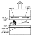
- FIG. 4 is a reference diagram showing a general PDP discharge cell configuration and discharge formation mechanism.
- Figure 5 is a graph showing the results of the element distribution changes before (a) and after (b) the thermal process of the panel when the diffusion barrier is composed of SiO 2 material according to the present invention.
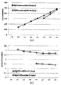
- FIG. 6 is a graph showing changes in voltage characteristics according to continuous discharge time of a panel to which SiO 2 is applied as a diffusion barrier and a panel to which the present invention is not applied.
- (B) is a graph showing the change in the sustain minimum voltage.
- FIG. 7 is a graph comparing luminance and luminous efficiency of a panel to which SiO 2 is applied as a diffusion barrier according to the present invention and a panel (a conventional panel) not to be applied.
- FIG. 8 is a cross-sectional view illustrating a plasma display panel according to another embodiment of the present invention, showing a structure in which a multilayer protective film is applied on a diffusion barrier.
- 9 to 10 are diagrams for explaining another embodiment of the present invention.
- FIG. 9 is a panel in which SiO 2 is applied as a diffusion barrier, a panel in which a mixture of alkali metal oxides (MgSrO) is applied as a protective film, and a voltage according to continuous discharge time of a panel to which a single component protective film made of MgO is applied.
- a is a graph showing the change in the minimum discharge starting voltage (Firing minimum voltage)
- b) is a graph showing the change in the sustain minimum voltage (Sustain minimum voltage).
- FIG. 10 shows panel characteristics according to the discharge voltage of a panel to which SiO 2 is applied as a diffusion barrier, a panel to which a mixture of alkaline earth metal oxides (MgSrO) is applied as a protective film, and a panel to which a single component protective film made of MgO is applied.
- a is a graph showing the change in luminance according to the voltage change
- b is a graph showing the change in luminous efficiency according to the voltage change.
- the transparent substrate 11, the bus electrode 13, the dielectric layer 15, the diffusion barrier 16, and the passivation layer 17 are formed on the front substrate 10 to form the front substrate assembly 10A.
- the address electrode 21, the dielectric layer 23, the partition wall 25, and the phosphor 27 are formed in the 20.
- the configuration of the fluorescent material 27 and the like is a well-known configuration, a detailed description thereof will be omitted, and the diffusion preventing film 16, which is a main characteristic component of the present invention, is provided on the diffusion preventing film 16.
- the protective film 17 is mainly described.
- the diffusion barrier 16 is composed of one layer or a plurality of layers between the dielectric layer 15 and the passivation layer 17.
- an encapsulation process and an exhaust process performed after the passivation layer 17 is formed.
- the impurity components existing in the front substrate 10, the dielectric layer 15, and the like may be prevented from being diffused into the protective layer 17.
- the diffusion barrier 16 is preferably made of a material having electrical insulation, that is, of an insulating material and excellent in transparency to visible light so that a voltage applied to the electrode can cause discharge in the cell space.
- the material constituting the diffusion barrier 16 is preferably composed of SiO 2 or a material containing SiO 2 , not a metallic material, but is not limited thereto, and Si 3 N 4 or SiON, Al 2 O 3 , At least one or more materials of TiO 2 , aC (amorphous carbon), and diamond may be mixed.
- any material having low diffusion rate, high light transmittance, and insulating properties such as Na, K, Al, and Ba may be applied.
- the diffusion barrier 16 may be composed of one layer or a plurality of layers between the dielectric layer 15 and the passivation layer 17. In the case of a plurality of layers, each layer may be composed of different materials.
- the diffusion barrier 16 is preferably configured to have a thickness of 0.01 ⁇ m to 5 ⁇ m between the dielectric layer 15 and the protective layer 17.
- the protective film 17 is preferably composed of MgO widely used as a protective film material of the PDP, but is not necessarily limited thereto.
- the configuration of another embodiment of the protective film configuration will be described below with reference to FIG. 8.
- the protective film 17 of MgO surface exists Mg (OH) 2 or contaminants that are generated by reacting with H 2 O and CO 2, such as MgCO 3, which in can be removed through the heat evacuation process of panel manufacturing process, but, Components of the materials (Na, K, Al, Ba, etc.) existing in the front substrate 10 and the dielectric layer 15 constituting the panel and diffused into the protective film 17 by heat applied from the outside during the panel manufacturing process are included. It was impossible to remove.
- the diffusion barrier 16 according to the present invention is an unnecessary component on the surface of the protective film 17 due to the diffusion of the components constituting the front substrate 10 and the dielectric layer 15 through the thermal process in the panel manufacturing process. It is possible to reduce the voltage of the panel and to increase the discharge efficiency by preventing the presence of the same. In addition, since the voltage stabilization time is relatively short after the start of the discharge, the process time devoted to the aging process for stabilizing the discharge can be reduced, and thus the lead time of manufacturing a commercial PDP ( Lead time can be shortened.
- the effect of reducing the discharge voltage due to the reduction of the impurity component in the protective film 17 in the PDP may contribute to improving the performance of the PDP by preventing the discharge characteristics of the panel from deteriorating over time.
- this characteristic can lower the sustain voltage in the panel, thereby lowering the overall power consumption and also lowering the address voltage for data writing.
- the sealing process of the front substrate 10 and the back substrate 20 After the protective film 17 is deposited on the front substrate 10, the sealing process of the front substrate 10 and the back substrate 20, and the hydrate (Mg) generated when the surface is exposed to the atmosphere containing H 2 O or CO 2
- a process in which heat of 400 ° C. or more is applied is essential.
- the micro components constituting the glass, the dielectric, etc. on the front substrate may be activated by heat to move between the thin films. This characteristic change can be easily confirmed by using a time of flight-secondary ion mass spectrometer (TOF-SIMS) capable of analyzing the microelements.
- TOF-SIMS time of flight-secondary ion mass spectrometer
- FIG. 3 shows the results of element distribution changes according to the thermal process (sealing process or exhaust process, etc.) when the MgO protective film 17 is applied.
- impurities Al, Na, K, etc.
- FIG. 3 shows the results of element distribution changes according to the thermal process (sealing process or exhaust process, etc.) when the MgO protective film 17 is applied.
- impurities Al, Na, K, etc.
- FIG. 3 shows the results of element distribution changes according to the thermal process (sealing process or exhaust process, etc.) when the MgO protective film 17 is applied.
- impurities Al, Na, K, etc.
- a discharge cell of a PDP includes one electrode facing two electrodes placed on a plane. Due to the discharge characteristics of the PDP using both the surface discharge and the counter discharge, the presence of impurity components on the surface of the protective film 17 such as MgO exposed to the discharge space greatly affects the discharge. In particular, many other components such as Al, Ba, K, etc. are also detected on the surface, but the appearance of Na on the surface acts as a major factor in reducing the efficiency of the panel and raising the initial discharge voltage. This will have a significant impact on panel performance.
- the diffusion barrier 16 between the dielectric layer 15 and the protective film 17 of the front substrate 10 the impurity components contained in the glass substrate and the dielectric are thermally protected. 17) It is possible to reduce power consumption by lowering the driving voltage as well as improving the performance of the PDP by preventing diffusion to the surface.
- FIG. 5 shows the results of element distribution changes before and after the thermal process of the panel when the diffusion barrier 16 is formed of SiO 2 material.
- the diffusion barrier 16 is formed of SiO 2 material with a thickness of 400nm
- the protective film 17 is a result of element distribution change using TOF-SIMS when formed with a 450nm thickness of MgO material.
- the impurity component is detected at a very low concentration, and in particular, as shown in FIG. Immediately after, it was confirmed that the impurity component was detected at a very low concentration on the surface of the protective film 17. Accordingly, it can be seen that the impurity component present on the surface of the protective film 17 is significantly reduced as compared with FIG. 3B (see dotted line regions of FIGS. 3B and 5B).
- plasma discharge generated in the PDP panel may be more easily generated, thereby lowering the discharge voltage.
- FIG. 6 shows voltage characteristics of a panel to which SiO 2 is applied as the diffusion barrier 16 and a panel to which no panel is applied.
- FIG. 6 (a) shows the state change according to the continuous discharge time of the firing minimum voltage at which the first cell is turned on when the voltage increases in the sustain discharge experiment
- FIG. 6 (b) shows the voltage decrease. Shows the state change according to the continuous discharge time of the sustain minimum voltage at which the discharge of all cells is turned off. 6, it can be confirmed that when SiO 2 is applied as the diffusion barrier layer 16, since the impurity component is hardly generated on the surface of the protective layer 17, the discharge voltage is lowered. This characteristic can lower the sustain voltage in the panel, thereby lowering the power consumption and reducing the address voltage.
- FIG. 7 is a view comparing luminance and luminous efficiency of a panel to which SiO 2 is applied as the diffusion barrier 16 and a panel to which no diffusion is applied. As shown in FIG. 7, when SiO 2 is applied as the diffusion barrier 16 (the present invention), the luminance and the efficiency are higher at the same voltage, and the light emission can be driven at a lower voltage than the conventional case. It shows that efficiency can be obtained.
- the diffusion barrier 16 provided between the dielectric layer 15 and the protective film 17 as described above can prevent the impurity components generated in the substrate glass and the dielectric from contaminating the protective film by thermal diffusion.
- the structure When applied to the structure can be expected to further improve the performance and shorten the aging process time.
- the protective film 17 formed on the diffusion barrier film 16 is composed of a first protective film 18 and a second protective film 19. It consists of.
- the second protective film 19 preferably functions to protect the first protective film 18 from the atmosphere before and after the front substrate and the rear substrate are bonded.
- the first passivation layer 18 is made of alkaline earth metal oxides and is formed on the diffusion barrier 16, and the second passivation layer 19 is formed of H 2 O in the atmosphere. Or on the first protective film 18 to prevent denaturation by reaction with CO 2 .
- the first passivation layer 18 may be an oxide composite or phase mixture or an oxide solid solution formed of any one or a combination of CaO, SrO, BaO, and BeO, which are alkaline earth metal oxides (Alkaline Earth Metal Oxides). It is preferred to be made of oxide solid solution). In the case of an oxide composite or an oxide solid solution, MgO may also be included in the combination.
- the material of the second protective film 19 is any one of CaO, SrO, BaO, MgO, BeO, SiO 2 , Si 3 N 4 , SiON, Al 2 O 3 , TiO 2 , aC (amorphous carbon) or diamond It is preferably formed of a composite formed of at least one composition, a solid solution, and the thickness thereof is preferably formed to have a thickness of 10 nm to 500 nm.
- the first passivation layer 18 and the second passivation layer 19 may be formed because these processes are high temperature thermal processes. ) Components are mixed with each other by thermal diffusion, and in particular, the first protective film 18 is diffused to the surface of the second protective film 19.
- the second protective film 19 The surface diffusion of the second protective film 19 including the first protective film 18 component becomes poor due to thermal diffusion to the surface, thereby increasing the discharge voltage. Therefore, the second protective film 19 contaminated with impurities needs to be completely removed through etching.
- the first protective layer 18 and the second protective layer 18 may be formed by impurity components diffused from the glass substrate and the dielectric. 19) can be prevented from being contaminated.
- Figure 2 is a view for explaining an embodiment of the present invention, since only the material constituting the protective film, with reference to FIG. It demonstrates, and the repeated description about the same similar component is abbreviate
- the protective film 17 is formed of a composite or solid solution of two or more alkaline earth metal oxides (Alkaline Earth Metal Oxides) is formed as a single layer on the diffusion barrier 16 It is also possible.
- the protective layer 17 may be made of an oxide composite or an oxide solid solution formed of a combination of one or more of alkaline earth metal oxides BeO, MgO, CaO, SrO, and BaO.
- the reactivity with H 2 O and CO 2 may be lowered while maintaining the unique characteristics of the alkaline earth metal oxide having a low band gap energy.
- the penetration of impurities contained in glass substrates or dielectrics into the protective film through thermal diffusion can be prevented by applying a diffusion barrier to shorten the aging time, lower the discharge voltage, and improve luminous efficiency. You can expect
- FIG. 9 is a graph showing changes in voltage characteristics according to continuous discharge time of a panel to which a protective film manufactured by E-beam deposition method and the like is not applied using a mixture of alkaline earth metal oxide mixed with MgO and SrO as an evaporation source. .
- FIG. 9 (a) shows the state change according to the continuous discharge time of the firing minimum voltage at which the first cell is turned on when the voltage increases in the sustain discharge experiment
- FIG. 6 (b) shows the voltage decrease. Shows the state change according to the continuous discharge time of the sustain minimum voltage at which the discharge of all cells is turned off.
- FIG. 10 is a panel in which SiO 2 is applied as a diffusion barrier, and a mixture of alkaline earth metal oxides mixed with MgO and SrO is used as an evaporation source. These graphs show changes in panel characteristics.
- Figure 10 (a) shows the change in luminance according to the voltage change
- Figure 10 (b) shows the change in luminous efficiency according to the voltage change.
Landscapes
- Physics & Mathematics (AREA)
- Engineering & Computer Science (AREA)
- Plasma & Fusion (AREA)
- Gas-Filled Discharge Tubes (AREA)
Abstract
본 발명에 따른 확산방지막이 구비된 플라즈마 디스플레이 패널은, 배면기판과 합착되어 플라즈마 디스플레이 패널을 구성하는 전면기판과, 상기 전면기판에서 상기 배면기판과 대향되는 면에 투명전극, 버스전극, 유전체층, 보호막이 순서대로 형성되되, 상기 유전체층과 보호막 사이에는, 전면기판 또는 유전체들로부터 불순물 성분들이 보호막 내로 확산되는 것을 방지하는 확산방지막이 더 구비됨으로써, 전면기판, 유전체 등에 존재하는 불순물 성분이 보호막으로 확산되는 것을 방지하여, 에이징(Aging) 초기에 방전을 안정화시키고, 낮은 전압에서 구동이 가능할 뿐만 아니라 패널의 방전효율을 높일 수 있는 효과를 제공한다.
Description
본 발명은 플라즈마 디스플레이 패널에 관한 것으로서, 특히 전면기판의 구성에 관한 것이다.
평판 디스플레이 장치 중의 하나인 플라즈마 디스플레이(또는 플라즈마 디스플레이 패널(Plasma Display Panel), 이하 "PDP"라고도 함)는, 가스방전에 의해 발생되는 자외선이 형광체를 여기 시킬 때 형광체로부터 발생하는 가시광선을 이용하여 화상을 표시하는 장치이다.
이러한 PDP는 두 장의 유리기판과 격벽을 이용하여 다수의 작은 공간을 만들고 그 공간에서 일어나는 플라즈마 방전의 조합으로 영상을 표현하는데, 플라즈마 방전을 발생시키기 위하여 방전가스를 사용한다. PDP 내부에 주입되는 가스는 He, Ne, Xe, Ar 등의 불활성가스가 주로 사용된다. 특히 진공 자외선의 생성원인 Xe에 Ne을 버퍼(buffer) 가스로 혼합된 형태가 널리 사용되고 있다.
Xe 가스의 첨가량은 플라즈마 디스플레이의 방전 특성에 매우 큰 영향을 끼치는 것으로 알려져 있다. 특히 전체 가스 중에서 Xe 가스의 부분압을 증가시킴으로써 플라즈마 디스플레이의 휘도 및 효율 특성을 향상시킬 수 있는데, 이러한 방법은 플라즈마 디스플레이의 가장 시급한 해결 과제 중 하나인 효율 문제를 해결할 수 있는 가장 효과적인 수단 중의 하나이다. 하지만 Xe 가스의 부분압 증가에 따라 방전 전압 역시 증가하여 안정적인 패널 방전이 어려울 뿐만 아니라, 디스플레이 소자의 안정적인 구동에 어려움이 생기고 전체적인 제품 생산에 필요한 비용이 증가하게 된다. 그러므로 플라즈마 디스플레이의 방전 특성 향상 및 타 디스플레이 대비 경쟁력 강화를 위해서 방전 전압을 대폭으로 낮출 수 있는 기술은 매우 중요하다.
한편, 플라즈마 디스플레이에서 보호막은 강한 방전현상으로부터 유전체막을 보호할 뿐만 아니라 이차전자방출을 통해서 방전전압을 낮추는 데에 큰 도움을 주는 것으로 알려져 있으며, 그러한 이유로 방전 특성 향상을 목적으로 다양한 보호막 관련 연구가 여러 연구 그룹에서 수행되어 왔다. 현재 플라즈마 디스플레이의 유전체 보호막으로 사용되는 MgO는 광투과도가 좋으면서도 이차전자방출 특성이 좋아 플라즈마 방전 전압을 낮추는데 크게 도움이 된다. 하지만 MgO는 Xe이온에 대해 이차전자 방출이 거의 없어 Xe 분압이 증가할수록 방전 전압이 같이 증가하기 때문에 고휘도 및 고효율에 대한 요구에 부응하기 위해 Xe가스 분압을 높이는데 어려움을 유발시키고 있다.
또한 플라즈마 디스플레이 패널(이하 '패널'이라고도 함)에는 유리기판 상에 서스테인(Sustain) 전극이 형성되고, 이 서스테인 전극 위에 유전체층이 구비되는데, 유리기판과 유전체층에는 불순물 성분이 존재하게 된다. 이들이 보호막 내로 확산될 경우에 보호막의 특성을 악화시켜 패널의 방전전압을 높이고 패널의 효율을 떨어뜨리게 된다. 특히, 패널 제조 공정에서, 보호막을 형성한 후에 진행되는 봉착, 가열 배기와 같은 고온 열공정 과정에서 이러한 전면기판 또는 유전체층의 불순물 성분이 보호막 표면으로 확산되는 것은 패널에서 방전전압이 높아지는 원인이 된다. 따라서 패널 내의 불순물 성분이 보호막 내로 확산되는 것을 방지하여 Xe이온에 의한 이차전자 방출량을 높이는 것이 중요하다.
MgO보다 낮은 밴드갭 에너지(Bandgap energy)를 갖는 알칼리토류 금속(Alkaline Earth Metal) 계열의 산화막이 보호막으로 사용될 경우 Xe이온에 의한 이차전자방출을 용이하게 할 수 있다. 하지만 이 물질들은 대기 중에서 H2O 또는 CO2와 매우 강하게 반응을 일으키고 결과적으로 수산화물(Hydroxide) 또는 탄산염(Carbonate)을 형성하는 특성을 가지고 있다. 통상적으로 대기 상태에서 공정이 진행되는 플라즈마 디스플레이 패널의 공정 특성상 MgO보다 낮은 밴드갭 에너지(Bandgap energy)를 갖는 알칼리토류 금속(Alkaline Earth Metal) 계열의 산화물만으로 방전 공간에 노출되어야만 하는 보호막을 구성할 경우, 상기의 H2O 또는 CO2와의 강한 반응성 때문에 보호막으로써 적용하기 어려웠으나, MgO보다 낮은 밴드갭 에너지를 가지는 알칼리토류 금속 산화물(Alkaline Earth Metal Oxides) 보호막 재료를 주보호막으로 하고, 대기 중의 물질과 반응성이 약한 BeO나 MgO와 같은 재료를 보조보호막으로 하는 다층 구조의 보호막을 구성함으로써 MgO보다 낮은 밴드갭에너지를 가지는 알칼리토류 금속(Alkaline Earth Metal) 계열의 산화물로 만들어지는 주보호막이 대기 중에서 H2O 또는 CO2와 반응하는 것을 억제시킬 수 있고, 이에 따라 보다 높은 휘도 및 효율의 플라즈마 디스플레이를 얻는 것이 가능하다.
그러나 상기한 바와 같이 주보호막과 보조보호막으로 구성된 다층박막구조로 패널을 제조할 경우에, 주보호막의 특성을 얻기 위해서는 식각 가스를 주입하여 보조보호막을 제거하고 Xe혼합가스를 주입하거나, 별도의 식각 가스를 주입하는 과정없이 Xe혼합가스를 처음부터 적용하여 장시간의 패널 에이징 공정(Aging process)을 통하여 보조보호막을 강한 방전을 이용한 스퍼터링으로 식각하는 방법이 있다. 이는 전체적인 패널 제조 공정 시간이 늘어나고, 생산성이 떨어지는 문제점이 발생될 수 있다.
이상 설명한 배경기술의 내용은 이 건 출원의 발명자가 본 발명의 도출을 위해 보유하고 있었거나, 본 발명의 도출 과정에서 습득한 기술 정보로서, 반드시 본 발명의 출원 전에 일반 공중에게 공개된 공지기술이라 할 수는 없다.
본 발명은 상기한 문제점을 해결하기 위하여 안출된 것으로서, 유전체층과 보호막 사이에 확산방지막을 구비함으로써, 유리기판, 유전체 등에 존재하는 불순물 성분이 보호막으로 확산되는 것을 방지하여, 패널의 방전 효율을 높일 수 있을 뿐만 아니라 방전 전압을 낮출 수 있는 확산방지막이 구비된 플라즈마 디스플레이 패널을 제공하는 데 목적이 있다.
또한 본 발명은, 에이징(Aging) 초기에 방전 전압을 안정화시킴으로써, 다층박막 구조를 적용한 구조에서도 보조보호막을 식각하지 않고서도 주보호막의 특성을 얻을 수 있어 에이징 공정(Aging process)에 소요되는 시간을 단축시킬 수 있는 확산방지막이 구비된 플라즈마 디스플레이 패널을 제공하는 데 목적이 있다.
또한 본 발명은, 확산방지막 위에 2종 이상의 알카리토류 금속 산화물의 혼합물로 보호막을 형성함으로써 낮은 밴드갭 에너지를 가지는 알카리토 금속의 고유한 특성을 살리면서도 H2O및 CO2와의 반응성을 저하시킬 수 있고, 유리기판, 유전체 등에 존재하는 불순물성분이 보호막으로 확산되는 것을 방지하는 확산방지막이 구비된 플라즈마 디스플레이 패널을 제공하는 데 목적이 있다.
상기한 과제를 실현하기 위한 본 발명에 따른 확산방지막이 구비된 플라즈마 디스플레이 패널은, 배면기판과 합착되어 플라즈마 디스플레이 패널을 구성하는 전면기판과, 상기 전면기판에서 상기 배면기판과 대향되는 면에 투명전극, 버스전극, 유전체층, 보호막이 순서대로 형성하되, 상기 유전체층과 보호막 사이에는, 전면기판 또는 유전체들로부터 불순물 성분들이 보호막 내로 확산되는 것을 방지하는 확산방지막이 더 구비된 것을 특징으로 한다.
이때, 상기 확산방지막은, 플라즈마 디스플레이 패널을 제조하는 과정에서, 상기 전면기판에 보호막을 형성한 후에 진행되는 전면기판과 배면기판의 합착 공정과 가열배기 공정 등의 고온 열처리 공정에서 전면기판 또는 유전체에 존재하고 있는 불순물 성분들이 보호막 내로 확산되는 것을 방지할 수 있도록 구성되는 것이 바람직하다.
상기 확산방지막은, 투명하고 전기 절연성을 갖는 물질로 이루어지는 것이 바람직하다.
이러한 상기 확산방지막은 SiO2소재를 포함하고, 한 층 또는 그 이상의 층으로 구성될 수 있다.
또한, 상기 확산방지막은 SiO2, Si3N4, SiON, Al2O3, TiO2, a-C(비정질탄소), 다이아몬드 중 적어도 어느 하나 또는 그 이상의 소재가 적용되어 구성되는 것도 가능하다. 이때 확산방지막은 다른 소재로 이루어진 복수의 층으로 구성될 수 있다.
확산방지막을 구성하는 소재는 상기한 소재 이외에도 Na, K, Al, Ba과 같은 물질들의 확산 속도가 낮고, 광투과도가 높으며 절연성질을 가지고 있는 물질이면 모두 적용이 가능하다.
상기 확산방지막은 0.01㎛ ~ 5㎛ 이하의 두께를 갖는 것이 바람직하다.
한편, 상기 보호막은 알칼리토류 금속 산화물(Alkaline Earth Metal Oxides)로 이루어져 상기 확산방지막 위에 형성되는 제1보호막과, 상기 제1보호막 위에 형성되어 상기 전면기판이 배면기판과 합착되기 전에 제1보호막이 대기 중에서 노출될 때 H2O 또는 CO2와 반응하여 변성되는 것을 방지하는 제2보호막으로 구성될 수 있다.
또한, 상기 보호막은 2종 이상의 알칼리토류 금속 산화물(Alkaline Earth Metal Oxides)의 복합체 또는 고용체로 이루어져 상기 확산방지막 위에 단일층으로 형성되는 것도 가능하다.
이때, 상기 보호막은, 알칼리토류 금속 산화물인 BeO, MgO, CaO, SrO, BaO 중 하나 이상의 조합으로 형성되는 산화물 복합체 또는 산화물 고용체로 구성되는 것이 바람직하다.
상기한 바와 같은 본 발명의 주요한 과제 해결 수단들은, 아래에서 설명될 '발명의 실시를 위한 구체적인 내용', 또는 첨부된 '도면' 등의 예시를 통해 보다 구체적이고 명확하게 설명될 것이며, 이때 상기한 바와 같은 주요한 과제 해결 수단 외에도, 본 발명에 따른 다양한 과제 해결 수단들이 추가로 제시되어 설명될 것이다.
본 발명에 따른 확산방지막이 구비된 플라즈마 디스플레이 패널은, 유전체층과 보호막 사이에 확산방지막이 구성되기 때문에 전면기판, 유전체 등에 존재하는 불순물 성분이 보호막으로 확산되는 것을 방지하여, 에이징(Aging) 초기에 방전을 안정화시키고, 방전전압을 낮추고, 패널의 방전효율을 높일 수 있는 효과가 있다.
즉, 본 발명은, 유전체층과 보호막 사이에 확산방지막이 구비됨으로써, 보호막 형성 후 플라즈마 디스플레이 패널 제조 공정상 필수적인 상판과 하판의 조립공정과 가열배기 공정 등의 고온 열처리 공정에서 패널 내 유리기판 또는 유전체의 구성 성분 등이 원하지 않은 부분으로 확산되거나, 공정 후에도 패널을 구성하고 있는 유리기판이나 유전체에 존재하고 있는 불순물 성분들이 보호막 내로 확산되는 것을 방지할 수 있게 된다. 이렇게 확산방지막을 통해 보호막 표면으로 불순물 성분이 확산되는 것을 방지함으로써 패널의 방전 효율을 높일 수 있을 뿐만 아니라, 방전 전압을 낮추는 효과가 있고, 이에 따라 패널의 성능 향상 및 소비전력 절감을 기대할 수 있으며, 특히 에이징(Aging) 공정 초기에 방전 전압을 안정화시킴으로써 다층보호막구조를 적용한 구조에서도 보조보호막을 식각할 필요가 없고, 에이징 공정에 소요되는 시간을 단축할 수 있는 효과가 있는 것이다.
또한 본 발명은 상기와 같은 확산방지막 위에 2종 이상의 알카리토류 금속 산화물의 혼합물로 보호막을 형성하는 경우에, 낮은 밴드갭 에너지를 가지는 알카리토 금속 산화물의 고유한 특성을 살리면서도 H2O및 CO2와의 반응성을 저하시킬 수 있고, 유리기판, 유전체 등에 존재하는 불순물 성분이 보호막으로 확산되는 것을 방지하여, 에이징(Aging) 초기에 방전을 안정화시킬 수 있고, 방전 전압을 낮출 수 있으며, 패널의 방전효율을 상승시킬 수 있는 효과를 갖는다.
도 1은 본 발명의 일 실시예에 따른 플라즈마 디스플레이 패널이 도시된 분해 상태의 사시도이다.
도 2는 본 발명의 일 실시예에 따른 플라즈마 디스플레이 패널이 도시된 단면 구성도이다.
도 3은 종래와 같이 유전체층 위에 MgO 보호막을 적용했을 경우에 패널 제조 과정에서, 열공정에 따른 원소 분포 변화의 결과를 보여주는 도면들로서, (a)는 보호막 형성 직후의 성분 변화를 보여주는 그래프이고, (b)는 고온 열처리 후의 성분 분포 변화를 보여주는 그래프이다.
도 4는 일반적인 PDP 방전셀 구성 및 방전 형성 메커니즘을 보여주는 참고도이다.
도 5는 본 발명에 따라 SiO2 소재로 확산방지막을 구성한 경우에 패널의 열공정 전(a)과 후(b)의 원소 분포 변화 결과를 보여주는 그래프들이다.
도 6은 본 발명에 따라 SiO2를 확산방지막으로 적용한 패널과 적용하지 않은 패널의 연속 방전 시간에 따른 전압특성 변화를 나타낸 그래프들로서, (a)는 최소방전개시전압(Firing minimum voltage)의 변화를 보여주는 그래프이고, (b)는 최소방전유지전압(Sustain minimum voltage)의 변화를 보여주는 그래프이다.
도 7은 본 발명에 따라 SiO2를 확산방지막으로 적용한 패널과 적용하지 않은 패널(종래 패널)의 휘도와 발광효율을 비교한 그래프이다.
도 8은 본 발명의 다른 실시예에 따른 플라즈마 디스플레이 패널이 도시된 단면 구성도로서, 확산방지막 위에 다층 보호막을 적용한 구조를 보여준다.
도 9 내지 도 10은 본 발명의 또 다른 실시예를 설명하기 위한 도면들이다.
도 9는 본 발명에 따라 SiO2를 확산방지막으로 적용한 패널에, 알카리토류 금속 산화물의 혼합물(MgSrO)을 보호막으로 적용한 패널과, MgO로 만들어진 단일 성분의 보호막이 적용된 패널의 연속 방전 시간에 따른 전압특성 변화를 나타낸 그래프들로서, (a)는 최소방전개시전압(Firing minimum voltage)의 변화를 보여주는 그래프이고, (b)는 최소방전유지전압(Sustain minimum voltage)의 변화를 보여주는 그래프이다.
도 10은 본 발명에 따라 SiO2를 확산방지막으로 적용한 패널에, 알카리토류 금속 산화물의 혼합물(MgSrO)을 보호막으로 적용한 패널과, MgO로 만들어진 단일 성분의 보호막이 적용된 패널의 방전전압에 따른 패널 특성 변화를 나타낸 그래프들로서, (a)는 전압변화에 따른 휘도변화를 보여주는 그래프이고, (b)는 전압 변화에 따른 발광 효율변화를 보여주는 그래프이다.
첨부된 도면을 참조하여 본 발명의 바람직한 실시 예를 설명하면 다음과 같다.
도 1 및 도 2를 참조하면, 본 발명에 따른 플라즈마 디스플레이 패널(이하 'PDP' 또는 '패널'이라고도 함)은, 전면기판(10)과 배면기판(20)으로 구성된다.
전면기판(10)에는 투명전극(11), 버스전극(13), 유전체층(15), 확산방지막(16), 보호막(17)이 형성되어 전면기판 어셈블리(10A)를 구성하게 되고, 배면기판(20)에는 어드레스 전극(21), 유전체층(23), 격벽(25) 및 형광체(27)가 구성된다.
PDP에서 전면기판(10)에 구성되는 투명전극(11), 버스전극(13), 유전체층(15) 및 배면기판(20)에 구성되는 어드레스 전극(21), 유전체층(23), 격벽(25) 및 형광체(27) 등의 구성은 널리 알려진 공지의 구성이므로 그에 대한 구체적인 설명은 생략하고, 본 발명의 주요 특징적인 구성 부분인 확산방지막(16)과, 이 확산방지막(16)의 상부에 구비되는 보호막(17)을 중심으로 설명한다.
상기 확산방지막(16)은 유전체층(15)과 보호막(17) 사이에 하나의 층 또는 복수의 층으로 구성되어, 플라즈마 디스플레이 패널 제조 공정에서, 상기 보호막(17)이 형성된 후에 진행되는 봉착공정, 배기공정과 같은 고온 열처리 공정에서 전면기판(10), 유전체층(15) 등에 존재하고 있는 불순물 성분들이 보호막(17) 내로 확산되는 것을 방지하는 역할을 한다.
이러한 확산방지막(16)은, 전극에 가해지는 전압이 셀 공간에서 방전을 일으킬 수 있도록 전기 절연성을 갖는 물질 즉, 절연 물질로 이루어지고 가시광에 대한 투과성이 우수한 물질로 이루어지는 것이 바람직하다.
확산방지막(16)을 구성하는 소재로는 금속성 물질이 아닌 SiO2 또는, SiO2를 포함하는 소재로 구성되는 것이 바람직하나, 이에 한정되는 것은 아니고, Si3N4 또는 SiON, Al2O3, TiO2, a-C(비정질탄소), 다이아몬드 중 적어도 어느 하나 또는 그 이상의 소재가 혼합되어 구성될 수 있다.
확산방지막을 구성하는 소재는 이외에도 Na, K, Al, Ba과 같은 물질들의 확산 속도가 낮고, 광투과도가 높으며 절연성질을 가지고 있는 물질이면 모두 적용이 가능하다.
또한 확산방지막(16)은 유전체층(15)과 보호막(17) 사이에 하나의 층 또는 그 이상의 복수의 층으로 구성될 수 있다. 복수의 층으로 이루어질 경우에 각 층은 다른 소재로 이루어져 구성될 수도 있다.
이와 같은 확산방지막(16)은 유전체층(15)과 보호막(17) 사이에 0.01㎛ ~ 5㎛ 이하의 두께를 갖도록 구성되는 것이 바람직하다.
한편, 상기 보호막(17)은 PDP의 보호막 소재로 널리 사용되는 MgO로 구성되는 것이 바람직하나, 반드시 이에 한정되는 것은 아니다. 보호막 구성에 대한 다른 실시예의 구성에 대해서는 도 8을 참조하여 아래에서 다시 설명한다.
상기한 바와 같이 전면기판에 구성되는 유전체층(15), 보호막(17) 사이에 확산방지막(16)을 설치하는 이유 및 그 작용, 그리고 효과 등에 대해, 도 3 내지 도 7을 참조하여, 자세히 설명하면 다음과 같다.
일반적으로 보호막(17)인 MgO 표면에 존재하는 Mg(OH)2나 MgCO3와 같이 H2O나 CO2 등과 반응하여 생성되는 불순물 성분은 패널 제조 과정 중 가열배기공정을 통하여 제거할 수 있지만, 패널을 구성하는 전면기판(10), 유전체층(15) 내에 존재하면서, 패널 제조 과정 중에 외부로부터 가해지는 열에 의해 보호막(17) 내로 확산되어지는 물질(Na, K, Al, Ba 등)의 성분을 제거하는 것은 불가능하였다.
하지만, 본 발명에 따라 구성되는 확산방지막(16)은 전면기판(10), 유전체층(15)을 구성하는 성분이 패널 제조 과정에서의 열공정을 통한 확산으로 인하여, 보호막(17) 표면에 불필요한 성분으로 존재하게 되는 것을 방지함으로써 패널의 전압을 낮추고 방전 효율을 높일 수 있게 된다. 또한 방전개시 후 전압이 안정화되는 시간이 상대적으로 짧기 때문에 방전안정화를 위해 실시하는 에이징(Aging) 공정에 할애되는 공정 시간(process time)을 감소시킬 수 있고, 이에 따라 상용 PDP의 제조의 리드 타임(lead time)을 단축할 수 있게 된다.
PDP에서 보호막(17) 내에 불순물 성분의 감소로 인한 방전 전압 저감효과는 패널의 경시적인 방전 특성 저하를 방지함으로써 PDP의 성능 개선에 기여할 수 있다. 또한 이러한 특성은 패널에서의 서스테인(Sustain) 전압을 낮출 수 있게 되어, 전체적으로 소비전력을 낮출 수 있을 뿐만 아니라 데이터 기입을 위한 어드레스(Address) 전압도 낮출 수 있게 된다.
전면기판(10)에 보호막(17)이 증착된 이후, 전면기판(10)과 배면기판(20)의 봉착공정과, 표면이 H2O나 CO2를 포함한 대기에 노출될 경우 생기는 수화물(Mg(OH)2)이나 탄산화물(MgCO3)과 같은 불순물을 제거하기 위한 배기 공정은 400℃ 이상의 열이 가해지는 공정이 필수적이다. 이 때, 전면기판에서 유리, 유전체 등을 구성하는 미소 성분이 열에 의해 활성화 되어 박막 사이를 이동할 수 있다. 이러한 특성변화는 미소 원소량 분석이 가능한 TOF-SIMS(Time Of Flight - Secondary Ion Mass Spectrometer)를 이용하면 쉽게 확인할 수 있다.
도 3은 MgO 보호막(17)을 적용했을 경우에 열공정(봉착공정 또는 배기공정 등)에 따른 원소 분포 변화 결과를 보여준다. 열처리 전에는 도 3의 (a)에 나타난 바와 같이 보호막의 표면에 불순물(Al,Na,K 등)이 매우 낮은 농도로 검출되지만, 열공정을 진행한 후에는 도 3의 (b)에 나타난 바와 같이 유전체층에서 나타나는 여러 가지 불순물 성분(Al, Na, K 등)이 높은 농도로 MgO 보호막 표면에서도 검출되었다는 것을 알 수 있다.
도 4를 참고하면, 일반적으로 PDP의 방전 셀은 평면상에 놓은 두 개의 전극과 마주보는 한 개의 전극으로 구성되어 있다. 면방전과 대향방전을 모두 이용하는 PDP의 방전 특성상 방전공간에 노출되는 MgO와 같은 보호막(17) 표면의 불순물 성분의 존재가 방전에 크게 영향을 미치게 된다. 특히, Al, Ba, K 등 다른 여러 성분도 표면에서 검출되지만 Na성분이 표면에서 나타나는 것은 패널의 효율을 반감시키고 초기 방전 전압을 상승시키는 주요인으로 작용하게 되므로, 이러한 미소 성분이 표면으로 확산하는 것을 막는 것은 패널 성능에 대단히 중요한 영향을 미치게 된다.
따라서, 상기한 바와 같이 전면기판(10)에 구성되는 유전체층(15)과 보호막(17) 사이에 확산방지막(16)을 구성함으로써, 유리기판, 유전체에 포함된 불순물 성분이 열 공정을 통해 보호막(17) 표면으로 확산되는 것을 방지함으로써 PDP의 성능 개선은 물론 구동 전압을 낮춰서 소비전력을 줄일 수 있게 되는 것이다.
이러한 효과를 도 5 내지 도 7을 참조하여 설명한다.
도 5는 SiO2 소재로 확산방지막(16)을 구성한 경우에 패널의 열공정 전후의 원소 분포 변화 결과를 보여준다. 이때, 확산방지막(16)은 SiO2 소재로 400㎚ 두께로 형성하고, 보호막(17)은 MgO 소재로 450㎚ 두께로 형성했을 때의 TOF-SIMS를 이용한 원소 분포 변화 결과이다.
도 5의 (a)에서 나타난 바와 같이 MgO 보호막(17)을 증착한 직후에 불순물 성분이 매우 낮은 농도로 검출되고, 특히 도 5의 (b)에서 나타난 바와 같이 봉착공정에서 400℃이상으로 소성한 직후에도 보호막(17) 표면에 불순물 성분이 매우 낮은 농도로 검출되었다는 것을 확인할 수 있다. 따라서, 도 3의 (b)와 비교했을 때 보호막(17) 표면에 존재하는 불순물 성분이 현저히 감소되는 것을 알 수 있다(도 3의 (b) 및 도 5의 (b) 점선 영역 참조).
이와 같이 확산방지막(16)의 역할에 의해 보호막(17) 표면에서 불순물 성분을 감소시킴으로써 PDP 패널 내에서 발생하는 플라즈마 방전을 보다 쉽게 발생시킬 수 있고, 이에 따라 방전 전압을 낮추는 효과를 가져 올 수 있음은 물론, 경시적 방전 특성 저하를 방지함으로써 PDP의 성능 개선에 기여할 수 있게 되는 것이다.
도 6은 SiO2를 확산방지막(16)으로 적용한 패널과 적용하지 않은 패널의 전압특성을 나타낸 것이다.
도 6의 (a)는 서스테인 방전 실험에서 전압 증가시 최초의 셀이 켜지는 최소방전개시전압(Firing minimum voltage)의 연속 방전 시간에 따른 상태 변화를 보여주고, 도 6의 (b)는 전압 감소시 모든 셀의 방전이 꺼지게 되는 최소방전유지전압(Sustain minimum voltage)의 연속 방전 시간에 따른 상태 변화를 보여준다. 도 6의 실험 결과를 통해 SiO2를 확산방지막(16)으로 적용할 경우에 보호막(17) 표면에 불순물 성분이 거의 발생하지 않게 됨에 따라 방전전압이 낮아지는 결과를 얻을 수 있다는 것을 확인할 수 있다. 이러한 특성은 패널에서의 서스테인 전압을 낮출 수 있고, 이에 따라 소비전력을 낮출 수 있을 뿐만 아니라 어드레스(Address) 전압도 낮출 수 있는 효과를 갖게 된다.
도 7은 SiO2를 확산방지막(16)으로 적용한 패널과 적용하지 않은 패널의 휘도와 발광효율을 비교한 도면이다. 도 7에 나타난 바와 같이 SiO2를 확산방지막(16)으로 적용한 경우(본 발명), 그렇지 않은 경우(종래)에 비해 동일 전압에서 휘도와 효율이 높아지고, 더 낮은 전압에서 구동이 가능하면서도 보다 높은 발광효율을 얻을 수 있음을 보여주고 있다.
한편, 상기한 바와 같은 유전체층(15)과 보호막(17) 사이에 구비되는 확산방지막(16)은 기판유리, 유전체에서 발생하는 불순물 성분이 열확산에 의해 보호막을 오염시키는 것을 방지할 수 있기 때문에 다층 보호막 구조에 적용할 경우 더욱 우수한 성능 향상과 에이징 공정 시간을 단축할 수 있는 효과를 기대할 수 있다.
이에 대하여 도 8을 참조하여 설명한다.
도 8에 예시된 본 발명의 다른 실시예에서는, 확산방지막(16) 위에 구성되는 보호막(17)이 제1보호막(18)과 제2보호막(19)으로 이루어져 전체적으로 2중 또는 그 이상의 다중막 구조로 구성된다. 이때 제2보호막(19)은 전면기판과 배면기판이 합착되기 전후에 대기로부터 제1보호막(18)을 보호하기 기능을 하는 것이 바람직하다.
즉, 제1보호막(18)은 알칼리토류 금속 산화물(Alkaline Earth Metal Oxides)로 이루어져 상기 확산방지막(16) 위에 형성되고, 제2보호막(19)은 제1보호막(18)이 대기 중에서 H2O 또는 CO2와의 반응하여 변성되는 것을 막아주도록 제1보호막(18) 위에 형성된다.
이와 같은 제1보호막(18)은 알칼리토류 금속 산화물(Alkaline Earth Metal Oxides)인 CaO, SrO, BaO, BeO 중 어느 하나 또는 하나 이상의 조합으로 형성되는 산화물 복합체(Oxides composite or Phase mixture) 혹은 산화물 고용체(Oxides solid solution)로 만들어지는 것이 바람직하다. 산화물 복합체 혹은 산화물 고용체인 경우 상기 조합에 MgO도 포함될 수 있다.
그리고 상기 제2보호막(19)의 재질은 CaO, SrO, BaO, MgO, BeO, SiO2, Si3N4, SiON, Al2O3, TiO2, a-C(비정질탄소) 또는 다이아몬드 중 어느 하나 또는 하나 이상의 조성으로 형성되는 복합체, 고용체로 형성되는 것이 바람직하고, 그 두께는 10nm ~ 500nm의 두께를 갖도록 형성되는 것이 바람직하다.
위와 같은 본 발명의 다른 실시예의 작용 및 효과를 설명하면 다음과 같다.
다중 보호막의 경우 보호막 증착 후 전면기판(10)과 배면기판(미도시 됨) 간의 합착이나 가열배기 공정을 거치게 되면, 이들 공정이 고온 열공정인 관계로 제1보호막(18)과 제2보호막(19) 성분들이 열확산에 의해 서로 섞이게 되며, 특히 제1보호막(18) 성분이 제2보호막(19) 표면으로 확산을 하게 된다.
여기서, 만일 유전체층(15)와 제1보호막(18)사이에 불순물이 확산되는 것을 방지할 수 있는 막이 없다면 이와 동시에 전면기판(10)을 구성하는 유리 및 유전체에서 발생하는 불순물 성분이 제2보호막(19) 표면으로 열확산을 하게 되어 제1보호막(18) 성분이 포함된 제2보호막(19)의 표면성분이 열악해져 방전 전압이 높아지게 된다. 따라서 불순물로 오염된 제2보호막(19)은 식각을 통해 완전 제거가 되어야 될 필요가 있다. 하지만, 본 발명에서와 같이 다중 보호막(17)과 유전체층(15) 사이에 확산방지막(16)이 존재하게 되면 유리기판과 유전체로부터 확산되는 불순물 성분에 의해 제1보호막(18)과 제2보호막(19)이 오염되는 것을 막을 수 있기 때문에 필요에 따라 제2보호막(19)을 제거하지 않더라도 제1보호막(18)의 우수한 성질이 곧바로 나타나므로 가열 배기 및 방전가스주입 후 통상의 에이징 공정 과정으로 프로세스를 진행할 수 있으며, 확산방지막(16)을 적용하지 않을 경우에 비해 더 낮은 전압에서 구동이 가능하고, 동일 전압에서 더 높은 휘도와 발광효율을 얻을 수 있을 뿐만 아니라 방전 안정화를 위한 에이징 시간을 더 짧게 할 수 있는 장점이 있다.
도 9 내지 도 10을 참조하여, 본 발명의 또 다른 실시예에 대하여 설명한다.
본 발명의 또 따른 실시예를 설명함에 있어서, 도 2는 본 발명의 일 실시예를 설명하기 위한 도면이나, 보호막을 구성하는 재질만 달리하므로, 도 2를 참조하여 일 실시예와 다른 부분을 중심으로 설명하고, 동일 유사한 구성 부분에 대해서는 반복 설명은 상략한다.
본 발명의 또 다른 실시예에서는, 도 2를 참조하면, 보호막(17)이 2종 이상의 알칼리토류 금속 산화물(Alkaline Earth Metal Oxides)의 복합체 혹은 고용체로 이루어져 확산방지막(16) 위에 단일층으로 형성되는 것도 가능하다.
이때, 상기 보호막(17)은, 알칼리토류 금속 산화물인 BeO, MgO, CaO, SrO, BaO 중 하나 이상의 조합으로 형성되는 산화물 복합체 또는 산화물 고용체로 만들어질 수 있다.
이와 같이 보호막(17) 소재로 알카리토류 금속 산화물의 혼합물을 적용할 경우에 낮은 밴드갭 에너지를 가지는 알카리토류 금속 산화물의 고유한 특성을 살리면서도 H2O및 CO2와의 반응성을 저하시킬 수 있게 되며, 유리기판이나 유전체 등에 포함된 불순물이 열확산을 통해 보호막 내로 침투하는 것을 확산방지막의 적용에 의해 방지할 수 있어 에이징 시간을 단축시킬 수 있고, 방전 전압을 낮출 수 있으며, 발광효율이 개선되는 효과를 기대할 수 있다.
도 9는 MgO와 SrO가 혼합된 알카리토류 금속 산화물의 혼합물을 증발원으로 사용하여 E-beam 증착법 등으로 제작된 보호막을 적용한 패널과 적용하지 않은 패널의 연속 방전 시간에 따른 전압특성 변화를 나타낸 그래프들이다.
도 9의 (a)는 서스테인 방전 실험에서 전압 증가시 최초의 셀이 켜지는 최소방전개시전압(Firing minimum voltage)의 연속 방전 시간에 따른 상태 변화를 보여주고, 도 6의 (b)는 전압 감소시 모든 셀의 방전이 꺼지게 되는 최소방전유지전압(Sustain minimum voltage)의 연속 방전 시간에 따른 상태 변화를 보여준다.
도 9의 실험 결과를 통해 SiO2로 만들어진 확산방지막(16) 위에 MgO와 SrO가 혼합된 알카리토류 금속 산화물의 혼합물을 증발원으로 하여 E-beam 등으로 제작된 보호막을 적용한 경우에 보호막으로 MgO만 적용할 경우보다 방전전압이 낮아지는 결과를 얻을 수 있다는 것을 확인할 수 있다. 이러한 특성은 패널에서의 서스테인 전압을 낮출 수 있고, 이에 따라 소비전력을 낮출 수 있을 뿐만 아니라 어드레스(Address) 전압도 낮출 수 있는 효과를 갖게 된다.
도 10은 SiO2를 확산방지막으로 적용한 패널에, MgO와 SrO가 혼합된 알카리토류 금속 산화물의 혼합물을 증발원으로 하여, E-beam 등으로 제작된 보호막을 적용한 패널과 MgO만 적용한 패널의 방전전압에 따른 패널 특성 변화를 나타낸 그래프들이다.
도 10의 (a)는 전압변화에 따른 휘도변화를 보여주고, 도 10의 (b)는 전압 변화에 따른 발광 효율변화를 보여준다.
도 10의 실험 결과를 통해, SiO2로 만들어진 확산방지막(16)위에 MgO와 SrO가 혼합된 알카리토류 금속 산화물의 혼합물을 증발원으로 하여, E-beam 등으로 제작된 보호막을 적용한 경우에, 보호막으로 MgO만 적용할 경우보다 동일 전압에서 휘도와 효율이 높아지고, 또한 더 낮은 전압에서 구동이 가능하면서도 보다 높은 발광효율을 얻을 수 있음을 보여주고 있다.
상기한 바와 같은, 본 발명의 실시예들에서 설명한 기술적 사상들은 각각 독립적으로 실시될 수 있으며, 서로 조합되어 실시될 수 있다. 또한, 본 발명은 도면 및 발명의 상세한 설명에 기재된 실시예를 통하여 설명되었으나 이는 예시적인 것에 불과하며, 본 발명이 속하는 기술분야에서 통상의 지식을 가진 자라면 이로부터 다양한 변형 및 균등한 타 실시예가 가능하다. 따라서, 본 발명의 기술적 보호범위는 첨부된 특허청구범위에 의해 정해져야 할 것이다.
Claims (11)
- 배면기판과 합착되어 플라즈마 디스플레이 패널을 구성하는 전면기판과, 상기 전면기판에서 상기 배면기판과 대향되는 면에 투명전극, 버스전극, 유전체층, 보호막이 순서대로 형성되되,상기 유전체층과 보호막 사이에는, 전면기판 또는 유전체로부터 불순물 성분들이 보호막 내로 확산되는 것을 방지하는 확산방지막이 더 구비된 것을 특징으로 하는 확산방지막을 갖는 플라즈마 디스플레이 패널.
- 청구항 1에 있어서,상기 확산방지막은, 플라즈마 디스플레이 패널을 제조하는 과정에서, 상기 전면기판에 보호막을 형성한 후에 진행되는 고온 열처리 공정에서 전면기판 또는 유전체에 존재하고 있는 불순물 성분들이 보호막 내로 확산되는 것을 방지할 수 있도록 구성된 것을 특징으로 하는 확산방지막을 갖는 플라즈마 디스플레이 패널.
- 청구항 1에 있어서,상기 확산방지막은, 투명하고 전기 절연성을 갖는 물질로 이루어진 것을 특징으로 하는 확산방지막을 갖는 플라즈마 디스플레이 패널.
- 청구항 1에 있어서,상기 확산방지막은 SiO2소재를 포함하고, 한 층 또는 그 이상의 층으로 구성된 것을 특징으로 하는 확산방지막을 갖는 플라즈마 디스플레이 패널.
- 청구항 1에 있어서,상기 확산방지막은 SiO2, Si3N4, SiON, Al2O3, TiO2, a-C(비정질탄소), 다이아몬드 중 적어도 어느 하나 또는 그 이상의 소재가 적용되어 구성된 것을 특징으로 하는 확산방지막을 갖는 플라즈마 디스플레이 패널.
- 청구항 5에 있어서,상기 확산방지막은 다른 소재로 이루어진 복수의 층으로 구성된 것을 특징으로 하는 확산방지막을 갖는 플라즈마 디스플레이 패널.
- 청구항 1에 있어서,상기 확산방지막은 0.01㎛ ~ 5㎛ 이하의 두께를 갖는 것을 특징으로 하는 확산방지막을 갖는 플라즈마 디스플레이 패널.
- 청구항 1 내지 청구항 7 중 어느 한 항에 있어서,상기 보호막은 알칼리토류 금속 산화물(Alkaline Earth Metal Oxides)로 이루어져 상기 확산방지막 위에 형성되는 제1보호막과, 상기 제1보호막 위에 형성되어 상기 전면기판이 배면기판과 합착 및 가열 배기 공정 중에 제1보호막이 대기 중에서 노출될 때 H2O 또는 CO2와 반응하여 변성되는 것을 방지하는 제2보호막으로 구성된 것을 특징으로 하는 확산방지막을 갖는 플라즈마 디스플레이 패널.
- 청구항 8에 있어서,상기 제1보호막은 알칼리토류 금속 산화물인 CaO, SrO, BaO, MgO, BeO 중 어느 하나 또는 하나 이상의 조합으로 형성되는 산화물 복합체(Oxides composite or Phase mixture) 또는 산화물 고용체(Oxides solid solution)로 만들어지고,상기 제2보호막은 CaO, SrO, BaO, MgO, BeO, SiO2, Si3N4, SiON, Al2O3, TiO2, a-C(비정질탄소) 또는 다이아몬드 중 어느 하나 또는 하나 이상의 조성으로 형성되는 산화물 복합체 또는 산화물 고용체로 형성되는 것을 특징으로 하는 확산방지막을 갖는 플라즈마 디스플레이 패널.
- 청구항 1 내지 청구항 7 중 어느 한 항에 있어서,상기 보호막은 2종 이상의 알칼리토류 금속 산화물(Alkaline Earth Metal Oxides)의 복합체 또는 고용체로 이루어져 상기 확산방지막 위에 단일층으로 형성되는 것을 특징으로 하는 확산방지막을 갖는 플라즈마 디스플레이 패널.
- 청구항 10에 있어서,상기 보호막은, 알칼리토류 금속 산화물인 BeO, MgO, CaO, SrO, BaO 중 하나 이상의 조합으로 형성되는 산화물 복합체 또는 산화물 고용체로 구성된 것을 특징으로 하는 확산방지막을 갖는 플라즈마 디스플레이 패널.
Applications Claiming Priority (4)
| Application Number | Priority Date | Filing Date | Title |
|---|---|---|---|
| KR10-2010-0040832 | 2010-04-30 | ||
| KR20100040832 | 2010-04-30 | ||
| KR10-2010-0090380 | 2010-09-15 | ||
| KR20100090380A KR101191224B1 (ko) | 2010-04-30 | 2010-09-15 | 확산방지막이 구비된 플라즈마 디스플레이 패널 |
Publications (1)
| Publication Number | Publication Date |
|---|---|
| WO2011136443A1 true WO2011136443A1 (ko) | 2011-11-03 |
Family
ID=44861713
Family Applications (1)
| Application Number | Title | Priority Date | Filing Date |
|---|---|---|---|
| PCT/KR2010/006608 Ceased WO2011136443A1 (ko) | 2010-04-30 | 2010-09-29 | 확산방지막이 구비된 플라즈마 디스플레이 패널 |
Country Status (1)
| Country | Link |
|---|---|
| WO (1) | WO2011136443A1 (ko) |
Citations (4)
| Publication number | Priority date | Publication date | Assignee | Title |
|---|---|---|---|---|
| KR20000060374A (ko) * | 1999-03-15 | 2000-10-16 | 구자홍 | 플라즈마 표시장치의 기판구조 및 제조방법 |
| JP2006286324A (ja) * | 2005-03-31 | 2006-10-19 | Fujitsu Hitachi Plasma Display Ltd | プラズマディスプレイパネル |
| US20070152593A1 (en) * | 2006-01-04 | 2007-07-05 | Lg Electronics Inc. | Plasma display panel and method for producing the same |
| KR20090118266A (ko) * | 2008-05-13 | 2009-11-18 | 삼성에스디아이 주식회사 | 플라즈마 디스플레이 패널 |
-
2010
- 2010-09-29 WO PCT/KR2010/006608 patent/WO2011136443A1/ko not_active Ceased
Patent Citations (4)
| Publication number | Priority date | Publication date | Assignee | Title |
|---|---|---|---|---|
| KR20000060374A (ko) * | 1999-03-15 | 2000-10-16 | 구자홍 | 플라즈마 표시장치의 기판구조 및 제조방법 |
| JP2006286324A (ja) * | 2005-03-31 | 2006-10-19 | Fujitsu Hitachi Plasma Display Ltd | プラズマディスプレイパネル |
| US20070152593A1 (en) * | 2006-01-04 | 2007-07-05 | Lg Electronics Inc. | Plasma display panel and method for producing the same |
| KR20090118266A (ko) * | 2008-05-13 | 2009-11-18 | 삼성에스디아이 주식회사 | 플라즈마 디스플레이 패널 |
Similar Documents
| Publication | Publication Date | Title |
|---|---|---|
| US5977708A (en) | Glass material used in, and fabrication method of, a plasma display panel | |
| KR100284458B1 (ko) | 플라즈마디스플레이패널의제조방법 | |
| KR100919443B1 (ko) | 플라즈마 디스플레이 패널의 제조방법 및 그 제조장치 | |
| TW508610B (en) | Gas discharge type light emission apparatus and manufacturing method for the same | |
| WO2011136443A1 (ko) | 확산방지막이 구비된 플라즈마 디스플레이 패널 | |
| JP2004247068A (ja) | ガス放電パネル及びその製造方法 | |
| KR100329043B1 (ko) | 플라즈마디스플레이패널의게터및그의활성화방법 | |
| KR20070036254A (ko) | 평판 표시 장치 및 그의 제조방법 | |
| KR101191224B1 (ko) | 확산방지막이 구비된 플라즈마 디스플레이 패널 | |
| JP4360926B2 (ja) | プラズマディスプレイパネル | |
| KR20050071683A (ko) | 플라즈마 디스플레이 패널의 제조방법 | |
| JPH11135023A (ja) | プラズマディスプレイパネルおよびその製造方法 | |
| KR100719580B1 (ko) | 평판 디스플레이 장치 | |
| JP3912567B2 (ja) | ガス放電表示装置 | |
| JPH1125865A (ja) | プラズマディスプレイパネル | |
| US8058805B2 (en) | Plasma display panel | |
| JP4505548B2 (ja) | プラズマディスプレイパネル | |
| US8803423B2 (en) | Fluorescent lamp and image display apparatus | |
| JP5113912B2 (ja) | プラズマディスプレイパネルおよびその製造方法 | |
| KR100412087B1 (ko) | 이중 보호막을 구비한 플라즈마 디스플레이 패널 | |
| CN101341569B (zh) | 平面型显示装置 | |
| KR100684826B1 (ko) | 플라즈마 디스플레이 패널 및 그의 제조방법 | |
| KR100459883B1 (ko) | 플라즈마 표시 패널의 보호층 형성방법 | |
| JP2000021302A (ja) | プラズマディスプレイパネル及びその製造方法 | |
| KR100692032B1 (ko) | 플라즈마 디스플레이 패널 |
Legal Events
| Date | Code | Title | Description |
|---|---|---|---|
| 121 | Ep: the epo has been informed by wipo that ep was designated in this application |
Ref document number: 10850809 Country of ref document: EP Kind code of ref document: A1 |
|
| NENP | Non-entry into the national phase |
Ref country code: DE |
|
| 122 | Ep: pct application non-entry in european phase |
Ref document number: 10850809 Country of ref document: EP Kind code of ref document: A1 |