WO2011135896A1 - 半導体装置及びその製造方法 - Google Patents
半導体装置及びその製造方法 Download PDFInfo
- Publication number
- WO2011135896A1 WO2011135896A1 PCT/JP2011/053258 JP2011053258W WO2011135896A1 WO 2011135896 A1 WO2011135896 A1 WO 2011135896A1 JP 2011053258 W JP2011053258 W JP 2011053258W WO 2011135896 A1 WO2011135896 A1 WO 2011135896A1
- Authority
- WO
- WIPO (PCT)
- Prior art keywords
- layer
- film
- insulating layer
- buffer
- semiconductor device
- Prior art date
- Legal status (The legal status is an assumption and is not a legal conclusion. Google has not performed a legal analysis and makes no representation as to the accuracy of the status listed.)
- Ceased
Links
Images









Classifications
-
- H—ELECTRICITY
- H10—SEMICONDUCTOR DEVICES; ELECTRIC SOLID-STATE DEVICES NOT OTHERWISE PROVIDED FOR
- H10D—INORGANIC ELECTRIC SEMICONDUCTOR DEVICES
- H10D30/00—Field-effect transistors [FET]
- H10D30/60—Insulated-gate field-effect transistors [IGFET]
- H10D30/67—Thin-film transistors [TFT]
- H10D30/6704—Thin-film transistors [TFT] having supplementary regions or layers in the thin films or in the insulated bulk substrates for controlling properties of the device
- H10D30/6723—Thin-film transistors [TFT] having supplementary regions or layers in the thin films or in the insulated bulk substrates for controlling properties of the device having light shields
-
- G—PHYSICS
- G02—OPTICS
- G02F—OPTICAL DEVICES OR ARRANGEMENTS FOR THE CONTROL OF LIGHT BY MODIFICATION OF THE OPTICAL PROPERTIES OF THE MEDIA OF THE ELEMENTS INVOLVED THEREIN; NON-LINEAR OPTICS; FREQUENCY-CHANGING OF LIGHT; OPTICAL LOGIC ELEMENTS; OPTICAL ANALOGUE/DIGITAL CONVERTERS
- G02F1/00—Devices or arrangements for the control of the intensity, colour, phase, polarisation or direction of light arriving from an independent light source, e.g. switching, gating or modulating; Non-linear optics
- G02F1/01—Devices or arrangements for the control of the intensity, colour, phase, polarisation or direction of light arriving from an independent light source, e.g. switching, gating or modulating; Non-linear optics for the control of the intensity, phase, polarisation or colour
- G02F1/13—Devices or arrangements for the control of the intensity, colour, phase, polarisation or direction of light arriving from an independent light source, e.g. switching, gating or modulating; Non-linear optics for the control of the intensity, phase, polarisation or colour based on liquid crystals, e.g. single liquid crystal display cells
- G02F1/133—Constructional arrangements; Operation of liquid crystal cells; Circuit arrangements
- G02F1/136—Liquid crystal cells structurally associated with a semi-conducting layer or substrate, e.g. cells forming part of an integrated circuit
- G02F1/1362—Active matrix addressed cells
- G02F1/136209—Light shielding layers, e.g. black matrix, incorporated in the active matrix substrate, e.g. structurally associated with the switching element
-
- G—PHYSICS
- G02—OPTICS
- G02F—OPTICAL DEVICES OR ARRANGEMENTS FOR THE CONTROL OF LIGHT BY MODIFICATION OF THE OPTICAL PROPERTIES OF THE MEDIA OF THE ELEMENTS INVOLVED THEREIN; NON-LINEAR OPTICS; FREQUENCY-CHANGING OF LIGHT; OPTICAL LOGIC ELEMENTS; OPTICAL ANALOGUE/DIGITAL CONVERTERS
- G02F1/00—Devices or arrangements for the control of the intensity, colour, phase, polarisation or direction of light arriving from an independent light source, e.g. switching, gating or modulating; Non-linear optics
- G02F1/01—Devices or arrangements for the control of the intensity, colour, phase, polarisation or direction of light arriving from an independent light source, e.g. switching, gating or modulating; Non-linear optics for the control of the intensity, phase, polarisation or colour
- G02F1/13—Devices or arrangements for the control of the intensity, colour, phase, polarisation or direction of light arriving from an independent light source, e.g. switching, gating or modulating; Non-linear optics for the control of the intensity, phase, polarisation or colour based on liquid crystals, e.g. single liquid crystal display cells
- G02F1/133—Constructional arrangements; Operation of liquid crystal cells; Circuit arrangements
- G02F1/136—Liquid crystal cells structurally associated with a semi-conducting layer or substrate, e.g. cells forming part of an integrated circuit
- G02F1/1362—Active matrix addressed cells
- G02F1/136227—Through-hole connection of the pixel electrode to the active element through an insulation layer
-
- H—ELECTRICITY
- H10—SEMICONDUCTOR DEVICES; ELECTRIC SOLID-STATE DEVICES NOT OTHERWISE PROVIDED FOR
- H10D—INORGANIC ELECTRIC SEMICONDUCTOR DEVICES
- H10D86/00—Integrated devices formed in or on insulating or conducting substrates, e.g. formed in silicon-on-insulator [SOI] substrates or on stainless steel or glass substrates
- H10D86/40—Integrated devices formed in or on insulating or conducting substrates, e.g. formed in silicon-on-insulator [SOI] substrates or on stainless steel or glass substrates characterised by multiple TFTs
- H10D86/451—Integrated devices formed in or on insulating or conducting substrates, e.g. formed in silicon-on-insulator [SOI] substrates or on stainless steel or glass substrates characterised by multiple TFTs characterised by the compositions or shapes of the interlayer dielectrics
-
- H—ELECTRICITY
- H10—SEMICONDUCTOR DEVICES; ELECTRIC SOLID-STATE DEVICES NOT OTHERWISE PROVIDED FOR
- H10D—INORGANIC ELECTRIC SEMICONDUCTOR DEVICES
- H10D86/00—Integrated devices formed in or on insulating or conducting substrates, e.g. formed in silicon-on-insulator [SOI] substrates or on stainless steel or glass substrates
- H10D86/40—Integrated devices formed in or on insulating or conducting substrates, e.g. formed in silicon-on-insulator [SOI] substrates or on stainless steel or glass substrates characterised by multiple TFTs
- H10D86/60—Integrated devices formed in or on insulating or conducting substrates, e.g. formed in silicon-on-insulator [SOI] substrates or on stainless steel or glass substrates characterised by multiple TFTs wherein the TFTs are in active matrices
-
- H—ELECTRICITY
- H10—SEMICONDUCTOR DEVICES; ELECTRIC SOLID-STATE DEVICES NOT OTHERWISE PROVIDED FOR
- H10W—GENERIC PACKAGES, INTERCONNECTIONS, CONNECTORS OR OTHER CONSTRUCTIONAL DETAILS OF DEVICES COVERED BY CLASS H10
- H10W20/00—Interconnections in chips, wafers or substrates
- H10W20/01—Manufacture or treatment
- H10W20/071—Manufacture or treatment of dielectric parts thereof
- H10W20/081—Manufacture or treatment of dielectric parts thereof by forming openings in the dielectric parts
- H10W20/089—Manufacture or treatment of dielectric parts thereof by forming openings in the dielectric parts using processes for implementing desired shapes or dispositions of the openings, e.g. double patterning
Definitions
- the present invention relates to a semiconductor device having a light-shielding conductive layer and a method for manufacturing the same.
- a semiconductor device having a light-shielding conductive layer on a substrate is known.
- a semiconductor device for example, as disclosed in Japanese Patent Application Laid-Open No. 2002-108244, a light shielding film positioned between a thin film transistor and a substrate is connected to a constant potential source.
- Japanese Patent Laid-Open No. 2002-108244 discloses a manufacturing method in which a contact hole extending to a light shielding layer and a contact hole extending to a semiconductor layer are simultaneously formed.
- an electrical influence such as noise occurs due to a parasitic capacitance existing in the semiconductor device.
- a method of adjusting the potential of the conductive layer having a light shielding property is considered. Specifically, a configuration in which the conductive layer is connected to, for example, a source wiring and the potential of the conductive layer is controlled is considered.
- the etching time required for forming the conductive layer contact hole penetrating the plurality of layers is longer than the etching time required for forming the semiconductor layer contact hole extending to the semiconductor layer.
- the inside of the semiconductor layer contact hole is Etching is excessive. That is, since etching is performed while the contact hole extending to the conductive layer is formed, the semiconductor layer may be excessively etched in the semiconductor layer contact hole, and the semiconductor layer may be reduced in thickness or penetrated. .
- An object of the present invention is to prevent an excessive etching of a semiconductor layer when a contact hole extending to a semiconductor layer and a contact hole extending to a conductive layer are simultaneously formed by etching.
- a method for manufacturing a semiconductor device includes a conductive layer forming step of forming a light-shielding conductive layer on a substrate, and an insulating layer forming step of forming an insulating layer on the substrate and the conductive layer.
- a semiconductor layer forming step of forming an island-shaped semiconductor layer in either the insulating layer or on the insulating layer, and the insulating layer other than the region where the semiconductor layer is formed and on the conductive layer An insulating layer removing step for forming an insulating layer removing portion by removing a part of the insulating layer located on the substrate; an interlayer insulating layer forming step for forming an interlayer insulating layer above the substrate; and a surface of the interlayer insulating layer A contact hole that simultaneously forms a semiconductor layer contact hole extending from the surface of the interlayer insulating layer to the semiconductor layer and a conductive layer contact hole extending from the surface of the interlayer insulating layer to the conductive layer through the insulating layer removing portion by etching. It has a Le forming step.
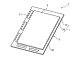
- FIG. 1 is a perspective view illustrating a schematic configuration of a display panel of a liquid crystal display device including the semiconductor device according to the first embodiment.
- FIG. 2 is a cross-sectional view illustrating a schematic configuration of the semiconductor device according to the first embodiment.
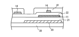
- FIG. 3A is a diagram illustrating a state in which a resist pattern for forming a removal portion is formed in the manufacturing process of the semiconductor device according to the first embodiment.
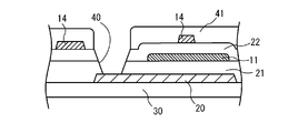
- FIG. 3B is a diagram illustrating a state where a removal portion is formed in the manufacturing process of the semiconductor device according to the first embodiment.
- FIG. 3C is a diagram illustrating a state in which a resist pattern for forming a contact hole is formed in the manufacturing process of the semiconductor device according to the first embodiment.
- FIG. 3A is a diagram illustrating a state in which a resist pattern for forming a removal portion is formed in the manufacturing process of the semiconductor device according to the first embodiment.
- FIG. 3B is a diagram illustrating a state where a removal portion is
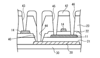
- FIG. 3D is a diagram illustrating a state in which the contact hole is formed in the manufacturing process of the semiconductor device according to the first embodiment.
- FIG. 3E is a diagram illustrating a state in which the wiring, the protective film, and the transparent electrode are formed in the manufacturing process of the semiconductor device according to the first embodiment.
- FIG. 4 is a cross-sectional view illustrating a schematic configuration of the semiconductor device according to the second embodiment.
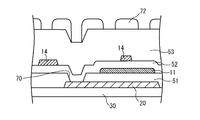
- FIG. 5A is a diagram illustrating a state in which a resist pattern for forming a removal portion is formed in the manufacturing process of the semiconductor device according to the second embodiment.
- FIG. 5B is a diagram illustrating a state in which a removal portion is formed in the manufacturing process of the semiconductor device according to the second embodiment.
- FIG. 5C is a diagram illustrating a state in which a resist pattern for forming a contact hole is formed in the manufacturing process of the semiconductor device according to the second embodiment.
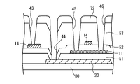
- FIG. 5D is a diagram illustrating a state in which contact holes are formed in the manufacturing process of the semiconductor device according to the second embodiment.
- FIG. 5E is a diagram illustrating a state in which wiring, a protective film, and a transparent electrode are formed in the manufacturing process of the semiconductor device according to the second embodiment.
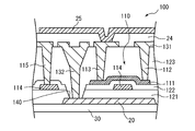
- FIG. 6 is a cross-sectional view illustrating a schematic configuration of the semiconductor device according to the third embodiment.
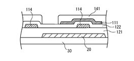
- FIG. 7A is a diagram illustrating a state in which a resist pattern for forming a removal portion is formed in the manufacturing process of the semiconductor device according to the third embodiment.
- FIG. 7B is a diagram illustrating a state in which a removal portion is formed in the manufacturing process of the semiconductor device according to the third embodiment.
- FIG. 7C is a diagram illustrating a state in which a resist pattern for forming a contact hole is formed in the manufacturing process of the semiconductor device according to the third embodiment.
- FIG. 7D is a diagram illustrating a state in which contact holes are formed in the manufacturing process of the semiconductor device according to the third embodiment.
- FIG. 7E is a diagram illustrating a state in which wiring, a protective film, and a transparent electrode are formed in the manufacturing process of the semiconductor device according to the third embodiment.
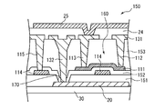
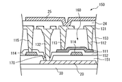
- FIG. 8 is a cross-sectional view showing a schematic configuration of the semiconductor device according to the fourth embodiment.
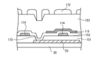
- FIG. 9A is a diagram illustrating a state in which a resist pattern for forming a removal portion is formed in the manufacturing process of the semiconductor device according to the fourth embodiment.
- FIG. 9B is a diagram illustrating a state where a removal portion is formed in the manufacturing process of the semiconductor device according to the fourth embodiment.
- FIG. 9C is a diagram illustrating a state in which a resist pattern for forming a contact hole is formed in the manufacturing process of the semiconductor device according to the fourth embodiment.
- FIG. 9D is a diagram illustrating a state in which contact holes are formed in the manufacturing process of the semiconductor device according to the fourth embodiment.
- FIG. 9E is a diagram illustrating a state in which the wiring, the protective film, and the transparent electrode are formed in the manufacturing process of the semiconductor device according to the fourth embodiment.
- a method of manufacturing a semiconductor device includes: a conductive layer forming step of forming a light-shielding conductive layer on a substrate; and an insulating layer formation for forming an insulating layer on the substrate and the conductive layer.
- the insulating layer includes a buffer layer and a gate insulating layer formed on the buffer layer.
- the buffer layer and the gate insulating layer located on the conductive layer are formed. It is preferable that a part of each layer is removed to form the insulating layer removal portion (second method).
- the time for forming the conductive layer contact hole is equal to or shorter than the time for forming the semiconductor layer contact hole in which at least the interlayer insulating layer needs to be etched. Therefore, since the etching time for forming the conductive layer contact hole and the semiconductor layer contact hole can be matched with the formation time of the semiconductor layer contact hole, it is possible to more reliably prevent the semiconductor layer from being excessively etched. .
- the insulating layer includes a buffer layer, and in the insulating layer removing step, a part of the buffer layer located on the conductive layer is removed to form the insulating layer removing portion. Is preferred (third method).
- a semiconductor layer is formed on the buffer layer so that the semiconductor layer is located between the buffer layer and the gate insulating layer.
- the interlayer insulating film and the gate insulating film In the stagger type (top gate type) semiconductor device obtained by this method, in order to reach the semiconductor layer contact hole to the semiconductor layer, the interlayer insulating film and the gate insulating film must be etched. Even in the semiconductor device having such a configuration, when the above-described second or third method is used, the interlayer insulating film, or the interlayer insulating film and the gate insulating film are etched when the conductive layer contact hole is formed. Good. Therefore, the time for forming the conductive layer contact hole is equal to or less than the time for forming the semiconductor layer contact hole. Therefore, when the conductive layer contact hole is formed, the semiconductor layer can be prevented from being excessively etched.
- a semiconductor layer is formed on the gate insulating layer formed on the buffer layer (fifth method).
- the inverted stagger type (bottom gate type) semiconductor device obtained by this method if the above-described second or third method is used, it is not necessary to remove the buffer layer when forming the conductive layer contact hole. Therefore, the time for forming the conductive layer contact hole can be shortened accordingly. Therefore, when the conductive layer contact hole is formed, the semiconductor layer can be prevented from being excessively etched.
- the method further includes a gate electrode forming step of forming a gate electrode on the insulating layer, and in the contact hole forming step, from the surface of the interlayer insulating layer to the gate electrode
- the extending gate electrode contact hole is preferably formed at the same time (sixth method).
- a semiconductor device includes a substrate, a light-shielding conductive layer formed on the substrate, an insulating layer formed on the substrate and the conductive layer, and in the insulating layer or A semiconductor layer formed on one of the insulating layers; an interlayer insulating layer formed over the substrate so as to cover the insulating layer and the semiconductor layer; and the conductive layer and the semiconductor in the interlayer insulating layer A wiring member extending to each of the layers, and the insulating layer is formed with an insulating layer removing portion in which at least a part of the conductive layer is removed except for the region where the semiconductor layer is formed. In the layer removal portion, the interlayer insulating layer and the wiring member extending to the conductive layer so as to penetrate the interlayer insulating layer are provided (seventh configuration).
- the insulating layer preferably includes a buffer layer and a gate insulating layer formed on the buffer layer (eighth configuration).
- the insulating layer includes a buffer layer, and the semiconductor layer is formed above the buffer layer (a ninth configuration).
- the semiconductor layer is provided on the buffer layer so as to be positioned between the buffer layer and a gate insulating layer formed on the buffer layer.
- the semiconductor layer is preferably provided on a gate insulating layer formed on the buffer layer (11th configuration).
- the dimension of the structural member in each figure does not represent the dimension of an actual structural member, the dimension ratio of each structural member, etc. faithfully.
- FIG. 1 shows a schematic configuration of a display panel 2 of a liquid crystal display device including the semiconductor device 1 according to the first embodiment. That is, the semiconductor device 1 according to the present embodiment is used for, for example, an active matrix substrate 3 constituting a display panel 2 of a liquid crystal display device.
- the display panel 2 includes an active matrix substrate 3, a counter substrate 4, and a liquid crystal layer (not shown) sandwiched between them.
- the display panel 2 is irradiated with light from a backlight device (not shown) of the liquid crystal display device.
- the active matrix substrate 3 includes a substrate 30 on which many pixels are formed in a matrix.
- the active matrix substrate 3 is provided with pixel electrodes and thin film transistors (TET: Thin Film Transistor, hereinafter referred to as “TFT”) corresponding to each pixel.
- TFT Thin Film Transistor
- the counter substrate 4 includes a counter electrode facing the pixel electrode and a color filter having a colored layer.
- the liquid crystal display device controls the liquid crystal in the liquid crystal layer by driving the TFT of the active matrix substrate 3 in accordance with a signal from the driver 5 provided on the active matrix substrate 3, and displays an image on the display panel 2. Is configured to display.
- FIG. 2 shows a schematic configuration of the semiconductor device 1 according to the present embodiment.
- the TFT 10 is formed on the substrate 30, and a light shielding film 20 (light-shielding conductive layer) is formed between the substrate 30 and the TFT 10.
- the light shielding film 20 is for preventing illumination light of the backlight device from being input to the TFT 10.
- the substrate 30 is a translucent glass substrate constituting the active matrix substrate 3, for example. In all the drawings showing the cross section (including FIG. 2), only conductors and semiconductors in the drawing are hatched.
- the TFT 10 is formed above the light shielding film 20 provided on the substrate 30. That is, the light shielding film 20 is formed in an island shape on the substrate 30, and the buffer film 21 is formed so as to cover the substrate 30 and the light shielding film 20.
- the light shielding film 20 is a metal film (for example, Mo, W / TaN, MoW, Ti / Ti) containing tantalum (Ta) or titanium (Ti), tungsten (W), molybdenum (Mo), aluminum (Al), or the like as a main component. Al).
- the buffer film 21 (insulating layer, buffer layer) is made of silicon oxide such as SiO 2 / SiNO or SiO 2 , SiN, silicon nitride, or the like.
- the TFT 10 has an island-shaped silicon film 11 (semiconductor layer) formed on the buffer film 21.
- the silicon film 11 is formed with a channel region and two semiconductor regions arranged in a plane so as to sandwich the channel region.
- the silicon film 11 is made of polycrystalline silicon such as continuous grain boundary silicon (CGS) or low-temperature poly-silicon (LPS), ⁇ -Si, or the like.
- Wires 12 and 13 are connected to the silicon film 11.
- the wiring 12 is connected to the source electrode 31.
- the wiring 13 is connected to the transparent electrode 25.
- the source electrode 31 is made of a metal material such as Ti / Al / Ti or Ti / Al, TiN / Al / TiN, Mo / Al—Nd / Mo, or Mo / Al / Mo.
- the transparent electrode 25 is made of a material such as ITO or ZnO.
- a gate insulating film 22 (insulating layer, gate insulating layer) is formed so as to cover the buffer film 21 and the silicon film 11.
- the gate insulating film 22 is made of SiO 2 or SiN, silicon oxide or silicon nitride such SiN / SiO 2.
- the buffer film 21 and the gate insulating film 22 correspond to an insulating layer.
- the gate electrode 14 of the TFT 10 is provided on the gate insulating film 22.
- the gate electrode 14 is made of a metal material such as W / TaN or Mo, MoW, Ti / Al.
- a wiring 15 (wiring member) is connected to the gate electrode 14. In the cross section shown in FIG. 2, the state in which the wiring 15 is connected to the gate electrode 14 on the right side is not shown, but as shown on the left side of FIG. A wiring 15 is connected to the gate electrode 14.
- an interlayer insulating film 23 (interlayer insulating layer) is formed on the gate insulating film 22 so as to cover the gate insulating film 22 and the gate electrode 14.
- a resin protective film 24 is formed on the interlayer insulating film 23.
- the wiring 32 (wiring member) is connected to the light shielding film 20 outside the region where the TFT 10 having the above-described configuration is formed.
- the wiring 32 is connected to the source electrode 31 although not particularly shown. Therefore, the potential of the light shielding film 20 is adjusted by the source electrode 31 through the wiring 32. As a result, the potential of the light shielding film 20 can be adjusted to reduce the influence of parasitic capacitance existing between the TFT 10 and the light shielding film 20.
- the wiring 32 is connected to the source electrode 31 in this embodiment, but may be connected to other wiring.
- the buffer film 21 and the gate insulating film 22 formed on the light shielding film 20 are surrounded by a portion surrounding the connection portion between the wiring 32 and the light shielding film 20.
- the removal part 40 (insulating layer removal part) from which the is removed is formed. That is, the buffer film 21 and the gate insulating film 22 are not formed on the light shielding film 20 around the connection portion with the wiring 32, and only the interlayer insulating film 23 is formed.
- FIGS. 3A to 3E are cross-sectional views showing the manufacturing process of the semiconductor device 1 in this embodiment.
- a light shielding film 20 is formed on the substrate 30 to prevent the illumination light of the backlight device from entering the TFT 10 from one surface side (the lower side in the figure) of the substrate 30. To do.
- a light-shielding thin film having a thickness of about 30 nm to 300 nm is formed on one surface (upper surface in the drawing) of the substrate 30 by a CVD (Chemical Vapor Deposition) method, a sputtering method, or the like.
- a resist pattern is formed by photolithography to cover a region where the light shielding film 20 is to be formed (hereinafter referred to as a region to be formed), and the light shielding thin film is etched using this resist pattern as a mask. Thereby, the light shielding film 20 is obtained.
- the light shielding film 20 is made of, for example, Mo.
- a buffer film 21 is formed so as to cover the substrate 30 and the light shielding film 20.
- the buffer film 21 is made of, for example, a laminated film of SiNO / SiO 2 .
- the buffer film 21 is formed with a thickness of about 100 nm to 400 nm by a CVD method.
- a silicon thin film made of, for example, CGS is formed on the buffer film 21 by a CVD method.
- This silicon thin film is formed to have a thickness of 30 nm to 100 nm.
- a resist pattern that covers a region where the silicon film 11 is to be formed is formed by photolithography, and the silicon thin film is etched using the resist pattern as a mask. Thereby, the silicon film 11 is obtained.
- the silicon film 11 is doped by ion implantation or the like, and a source region and a drain region (not shown) are formed in the silicon film 11.
- a gate insulating film 22 made of, for example, SiO 2 is formed on the buffer film 21 and the silicon film 11 by a CVD method.
- the gate insulating film 22 is formed to have a thickness of 50 nm to 200 nm.
- a metal film made of, for example, W / TaN is formed on the gate insulating film 22 by a sputtering method. This metal film is formed to have a thickness of 200 nm to 500 nm. Thereafter, a resist pattern that covers a region where the gate electrode 14 is to be formed is formed by photolithography, and the metal film is etched using the resist pattern as a mask. Thereby, the gate electrode 14 is obtained.
- a resist pattern 41 is formed on the gate insulating film 22 and the gate electrode 14 so as to be opened above the light shielding film 20 and in a portion other than the region where the silicon film 11 is formed. That is, the resist pattern 41 has an opening that exposes a region where the removal portion 40 is to be formed in the gate insulating film 22.
- the gate insulating film 22 and the buffer film 21 are etched using the resist pattern 41 as a mask. At this time, the gate insulating film 22 and the buffer film 21 are etched until the light shielding film 20 is exposed. As a result, the gate insulating film 22 and the buffer film 21 located above a part of the light shielding film 20 are removed, and the removal portion 40 is formed.
- 3B is performed by wet etching using buffered hydrofluoric acid (BHF) or etching gas (C 4 F 8 , SF 6 , CF 4 , O 2 , Ar, H 2, etc.).
- BHF buffered hydrofluoric acid
- etching gas C 4 F 8 , SF 6 , CF 4 , O 2 , Ar, H 2, etc.
- the dry etching used may be used.
- the method which combined these wet etching and dry etching may be used.
- an interlayer insulating film 23 made of, for example, a laminated film of SiO 2 / SiN is formed on the gate insulating film 22, the gate electrode 14, and the removal portion 40 by a CVD method. Form. Thereafter, a resist pattern 42 is formed on the interlayer insulating film 23.
- the resist pattern 42 has an opening that exposes regions where the contact holes 43 to 46 where the wirings 15, 32, 13, and 12 are to be formed are exposed.
- regions where the contact holes 46 and 45 are formed on the silicon film 11 in plan view (viewed from above). positioned. A region where a contact hole 43 (gate electrode contact hole) in which the wiring 15 is to be formed is located on the gate electrode 14 in plan view (viewed from above). A region in which the contact hole 44 (conductive layer contact hole) where the wiring 32 is to be formed is located in the removal portion 40 in plan view (viewed from above in the drawing).
- the interlayer insulating film 23 and the gate insulating film 22 are etched using the resist pattern 42 as a mask.
- contact holes 43 to 46 extending from the surface of the interlayer insulating film 23 to the gate electrode 14, the light shielding film 20, and the silicon film 11 are formed.
- the etching at this time is preferably dry etching using an etching gas. Note that not all etching is performed by dry etching, but wet etching may be performed after most of the etching is performed by dry etching.
- the buffer film 21 and the gate insulating film 22 are removed, and only the interlayer insulating film 23 is formed.
- the film thickness that needs to be etched is the thickest in the regions where the contact holes 45 and 46 of the wirings 12 and 13 connected to the silicon film 11 are to be formed. That is, in the regions where the contact holes 43 and 44 of the wirings 15 and 32 are to be formed, only the interlayer insulating film 23 needs to be etched, whereas in the regions where the contact holes 45 and 46 of the wirings 13 and 12 are to be formed, interlayer insulation is performed. It is necessary to etch the film 23 and the gate insulating film 22.
- the regions where the contact holes 43 to 46 are to be formed can be etched at a time based on the etching time of the regions where the contact holes 45 and 46 are to be formed. Therefore, it is possible to prevent the silicon film 11 from being excessively etched during the etching shown in FIG. 3D. Further, since the regions where the contact holes 43 and 44 of the wirings 15 and 32 are to be formed have substantially the same thickness of the interlayer insulating film 23, the gate electrode 14 is formed when the regions where the contact holes 43 and 44 are to be formed are etched simultaneously. Can be prevented from being excessively etched.
- the step of forming the light shielding film 20 on the substrate 30 is a conductive layer forming step
- the step of forming the buffer film 21 and the gate insulating film 22 on the substrate 30 and the light shielding film 20 is an insulating layer forming step.
- the step of forming the silicon film 11 on the buffer film 21 corresponds to the semiconductor layer forming step
- the step of forming the gate electrode 14 on the gate insulating film 22 corresponds to the gate electrode forming step.
- the step of forming the removal portion 40 by removing the buffer film 21 and the gate insulating film 22 located above a part of the light shielding film 20 is the insulating layer removing step, and the step of forming the interlayer insulating layer 23 is the interlayer insulation.
- the process of forming the contact holes 43 to 46 corresponds to the contact hole forming process.
- the interlayer insulating film 23 is formed after removing the buffer film 21 and the gate insulating film 22 formed on the light shielding film 20 in the portion where the wiring 32 is connected to the light shielding film 20. Then, the regions where the plurality of contact holes 43 to 46 are to be formed are etched simultaneously. This eliminates the need to etch the buffer film 21 and the gate insulating film 22 in the region where the contact hole 44 is to be formed in the wiring 32 when simultaneously etching the region where the plurality of contact holes 43 to 46 are to be formed.
- the silicon film 11 is formed in the formation regions of the contact holes 45 and 46 of the wirings 13 and 12 when simultaneously etching the formation regions of the contact holes 43 to 46. Excessive etching can be prevented.
- the TFT 10 in this embodiment is a so-called top gate type in which the silicon film 11 is located between the buffer film 21 and the gate insulating film 22 and the gate electrode 14 is formed on the gate insulating film 22. TFT. Therefore, the film thickness that needs to be etched is the thickest in the regions where the contact holes 45 and 46 of the wirings 12 and 13 connected to the silicon film 11 are to be formed. Therefore, since the regions where the other contact holes 43 and 44 are to be formed can be etched in accordance with the time for etching the regions where the contact holes 45 and 46 are to be formed, the silicon film 11 is reduced or penetrated by the etching. Can be more reliably prevented.
- the region where the contact hole 43 is to be formed in the wiring 15 connected to the gate electrode 14 and the region where the contact hole 44 is to be formed in the wiring 32 connected to the light shielding film 20 are the thickness of the interlayer insulating film 23 to be etched. Are almost the same. Therefore, it is possible to prevent the gate electrode 14 from being excessively etched when simultaneously forming the regions where the plurality of contact holes 43 to 46 are to be formed.
- FIG. 4 shows a schematic configuration of a semiconductor device 50 according to the second embodiment. This embodiment is different from the first embodiment in the configuration of the removal unit 70 and the method for manufacturing the semiconductor device 50.
- the same components as those in the first embodiment are denoted by the same reference numerals, and only different portions will be described.
- the removal portion 70 (insulating layer removal portion) is formed only in the buffer film 51 (insulating layer, buffer layer). That is, a gate insulating film 52 (gate insulating layer) is formed on the light shielding film 20 around the connection portion with the wiring 32, and an interlayer insulating film 53 (interlayer insulating layer) is formed on the gate insulating film 52. Is formed.
- This configuration shortens the time required for etching the formation region because the buffer film 51 does not exist in the formation region of the contact hole 44 of the wiring 32. Therefore, when the regions where the contact holes 43 to 46 of the wirings 15, 32, 13 and 12 are to be formed are etched simultaneously, the silicon film 11 connected to the wirings 12 and 13 and the gate electrode 14 connected to the wiring 15 are excessive. Etching can be suppressed.
- FIGS. 5A to 5E are cross-sectional views showing the manufacturing process of the semiconductor device 50 in this embodiment.
- the material and manufacturing method of each film constituting the semiconductor device 50 are the same as those in the first embodiment.
- the illumination light of the backlight device is prevented from being incident on the TFT 60 from one surface side (the lower side of the drawing) of the substrate 30 on the substrate 30.
- a light shielding film 20 is formed.
- a buffer film 51 is formed so as to cover the substrate 30 and the light shielding film 20.
- the silicon film 11 is formed on the buffer film 51 as in the first embodiment.
- a resist pattern 71 is formed on the buffer film 51 and the silicon film 11 by photolithography so as to be opened above the light shielding film 20 and in a portion other than the region where the silicon film 11 is formed. That is, the resist pattern 71 has an opening that exposes a region where the removal portion 70 is to be formed in the buffer film 51.
- the buffer film 51 is etched using the resist pattern 71 as a mask. At this time, the buffer film 51 is etched until the light shielding film 20 is exposed. As a result, the buffer film 51 located above a part of the light shielding film 20 is removed, and the removal portion 70 is formed.
- the etching in FIG. 5B may be wet etching or dry etching, as in the first embodiment. Moreover, the method which combined these wet etching and dry etching may be used.
- a gate insulating film 52 similar to that of the first embodiment is formed on the buffer film 51 and the silicon film 11, and a gate is formed on the gate insulating film 52.
- the electrode 14 is formed.
- an interlayer insulating film 53 is formed, and a resist pattern 72 having an opening that exposes regions where the contact holes 43 to 46 in which the wirings 15, 32, 13, and 12 are formed is exposed on the interlayer insulating film 53.
- regions where the contact holes 45 and 46 in which the wirings 13 and 12 are to be formed are located on the silicon film 11 in plan view (viewed from above).
- a region where the contact hole 43 where the wiring 15 is to be formed is located on the gate electrode 14 in plan view (viewed from above).
- a region where the contact hole 44 where the wiring 32 is to be formed is located in the removal portion 70 in plan view (as viewed from above).
- the interlayer insulating film 53 and the gate insulating film 52 are etched using the resist pattern 72 as a mask.
- contact holes 43 to 46 extending from the surface of the interlayer insulating film 53 to the gate electrode 14, the light shielding film 20, and the silicon film 11 are formed.
- the etching at this time is preferably dry etching using an etching gas. Note that it is not necessary to perform all etching by dry etching, and wet etching may be performed after most of the etching is performed by dry etching.
- the buffer film 51 is removed, and only the gate insulating film 52 and the interlayer insulating film 53 are formed. Therefore, the film thickness that needs to be etched in the region where the contact hole 44 is to be formed is equivalent to the film thickness that needs to be etched in the region where the contact holes 45 and 46 of the wirings 13 and 12 are to be formed. Therefore, it is possible to prevent the silicon film 11 to which the wirings 12 and 13 are connected from being excessively etched when etching is performed simultaneously in the regions where the plurality of contact holes 44 to 46 are to be formed.
- the wirings 15, 32, 13, 12 are formed in the contact holes 43 to 46, and the source electrode 31 is formed. Then, the protective film 24 and the transparent electrode 25 are formed on the interlayer insulating film 53. Thereby, the semiconductor device 50 is formed.
- the step of forming the light shielding film 20 on the substrate 30 corresponds to the conductive layer forming step
- the step of forming the buffer film 51 on the substrate 30 and the light shielding film 20 corresponds to the insulating layer forming step.
- the process of forming the silicon film 11 on the buffer film 51 corresponds to the semiconductor layer forming process
- the process of forming the gate electrode 14 on the gate insulating film 52 corresponds to the gate electrode forming process.
- the step of removing the buffer film 51 located above a part of the light shielding film 20 to form the removal portion 70 is the insulating layer removing step
- the step of forming the interlayer insulating layer 53 is the interlayer insulating layer forming step.
- the process of forming the contact holes 43 to 46 corresponds to the contact hole forming process.
- the gate insulating film 52 and the interlayer insulating film 53 are formed after removing the buffer film 51 formed on the light shielding film 20 in the portion where the wiring 32 is connected to the light shielding film 20. Then, the regions where the plurality of contact holes 43 to 46 are to be formed are etched simultaneously.
- the film thickness that needs to be etched in the region where the contact hole 44 of the wiring 32 is to be formed is the film thickness that needs to be etched in the region where the contact holes 45 and 46 of the wiring 13 and 12 connected to the silicon film 11 are to be formed.
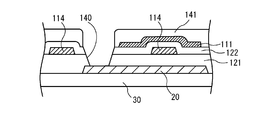
- FIG. 6 shows a schematic configuration of a semiconductor device 100 according to the third embodiment.
- the configuration of the TFT 110 is different from that of the first embodiment.
- the same components as those in the first embodiment are denoted by the same reference numerals, and only different portions will be described.
- the TFT 110 includes a silicon film 111 (semiconductor layer) formed on a gate insulating film 122 (insulating layer, gate insulating layer), and a buffer film 121 (insulating layer, buffer layer).
- a silicon film 111 semiconductor layer
- a gate insulating film 122 insulating layer, gate insulating layer
- a buffer film 121 insulating layer, buffer layer
- the wiring 132 (wiring member) connected to the light shielding film 20 is provided in the removing portion 140 (insulating layer removing portion) from which the buffer film 121 and the gate insulating film 122 are removed. That is, the removal portion 140 from which the buffer film 121 and the gate insulating film 122 are removed is formed on the light shielding film 20 around the connection portion with the wiring 132, and the interlayer insulation film 123 is formed in the removal portion 140. Is provided.
- the contact hole 144 of the wiring 132 is scheduled to be formed when the formation regions of the contact holes 143 to 146 (see FIG. 7D) of the wirings 115, 132, 113, and 112 are simultaneously etched.
- the etching time of the region can be shortened.
- FIGS. 7A to 7E are cross-sectional views showing the manufacturing process of the semiconductor device 100 in this embodiment.
- the material of each film constituting the semiconductor device 100 is the same as that in the first and second embodiments.
- the illumination light of the backlight device is prevented from entering the TFT 110 from one surface side (the lower side of the drawing) of the substrate 30 on the substrate 30.
- a light shielding film 20 is formed.
- a buffer film 121 is formed so as to cover the substrate 30 and the light shielding film 20.
- a metal film is formed on the buffer film 121 by sputtering. Thereafter, a resist pattern is formed by photolithography to cover a region where the gate electrode 114 is to be formed, and the metal film is etched using the resist pattern as a mask. Thereby, the gate electrode 114 is obtained.
- a gate insulating film 122 similar to that of the first embodiment is formed on the buffer film 121 and the gate electrode 114 by a CVD method.
- a silicon thin film is formed on the gate insulating film 122 by a CVD method.
- a resist pattern that covers a region where the silicon film 111 is to be formed is formed by photolithography, and the silicon thin film is etched using the resist pattern as a mask. Thereby, the silicon film 111 is obtained.
- a resist pattern 141 is formed on the gate insulating film 122 and the silicon film 111 so as to open above the light shielding film 20 and in a portion other than the region where the silicon film 111 is formed. That is, the resist pattern 141 has an opening that exposes a region where the removal portion 140 is to be formed in the gate insulating film 122.
- the gate insulating film 122 and the buffer film 121 are etched using the resist pattern 141 as a mask. At this time, the gate insulating film 122 and the buffer film 121 are etched until the light shielding film 20 is exposed. As a result, the gate insulating film 122 and the buffer film 121 located above a part of the light shielding film 20 are removed, and the removal portion 140 is formed.
- the etching in FIG. 7B may be wet etching or dry etching, as in the first embodiment. Moreover, the method which combined these wet etching and dry etching may be used.
- an interlayer insulating film 123 is formed on the gate insulating film 122, the silicon film 111, and the removal portion 140 by a CVD method. Thereafter, a resist pattern 142 is formed on the interlayer insulating film 123 so as to open regions where the contact holes 143 to 146 in which the wirings 115, 132, 113, and 112 are formed are opened.
- regions where the contact holes 145 and 146 semiconductor layer contact holes
- regions where the contact holes 145 and 146 semiconductor layer contact holes
- a region where the contact hole 143 (gate electrode contact hole) where the wiring 115 is to be formed is located on the gate electrode 114 in plan view (viewed from above).
- a region in which the contact hole 144 (conductive layer contact hole) where the wiring 132 is to be formed is located in the removal portion 140 in plan view (viewed from above).
- the interlayer insulating film 123 and the gate insulating film 122 are etched using the resist pattern 142 as a mask. Thereby, contact holes 143 to 146 extending from the surface of the interlayer insulating film 123 to the gate electrode 114, the light shielding film 20, and the silicon film 111 are formed.
- the etching at this time is preferably dry etching using an etching gas. Note that it is not necessary to perform all etching by dry etching, and wet etching may be performed after most of the etching is performed by dry etching.
- the buffer film 121 and the gate insulating film 122 are removed in the region where the contact hole 144 of the wiring 132 is to be formed, and only the interlayer insulating film 123 is formed. Therefore, the film thickness to be etched is the same in the region where the contact hole 144 of the wiring 132 is to be formed and the region where the contact holes 145 and 146 of the wiring 113 and 112 connected to the silicon film 111 are to be formed. Therefore, the silicon film 111 can be prevented from being excessively etched during the etching shown in FIG. 7D.
- the film thickness to be etched is the thickest in the region where the contact hole 143 of the wiring 115 connected to the gate electrode 114 is to be formed. Therefore, the plurality of contact holes 143 to 146 can be etched simultaneously with reference to the time for etching the region. Since the region where the contact hole 143 is to be formed is only thicker than the other region by the amount of the gate insulating film 122, when simultaneously etching the contact holes 143 to 146, the light shielding film 20 and the silicon film 111 are formed. Can be prevented from being excessively etched.
- wirings 115, 132, 113, 112 are formed in the contact holes 143 to 146, and a source electrode 131 is formed. Then, the protective film 24 and the transparent electrode 25 are formed on the interlayer insulating film 123. Thereby, the semiconductor device 100 is formed.
- the process of forming the light shielding film 20 on the substrate 30 is a conductive layer forming process
- the process of forming the buffer film 121 and the gate insulating film 122 on the substrate 30 and the light shielding film 20 is an insulating layer forming process.
- the step of forming the silicon film 111 over the gate insulating film 122 corresponds to the semiconductor layer forming step
- the step of forming the gate electrode 114 over the buffer film 121 corresponds to the gate electrode forming step.
- the step of forming the removal portion 140 by removing the buffer film 121 and the gate insulating film 122 located above a part of the light shielding film 20 is the insulating layer removing step, and the step of forming the interlayer insulating layer 123 is the interlayer insulation.
- the process of forming contact holes 143 to 146 corresponds to the contact hole forming process.
- the removal portion 140 is formed after the silicon film 111 is formed on the gate insulating film 122.
- the removal portion 140 may be formed before the silicon film 111 is formed.
- the interlayer insulating film 123 is formed after removing the buffer film 121 and the gate insulating film 122 formed on the light shielding film 20 in the portion where the wiring 132 is connected to the light shielding film 20. Then, the regions where the plurality of contact holes 143 to 146 are to be formed are etched simultaneously. As a result, the film thickness etched in the region where the contact hole 144 of the wiring 132 is to be formed and the film thickness etched in the region where the contact holes 145 and 146 of the wiring 113 and 112 connected to the silicon film 111 are formed are reduced. It becomes possible to make it equivalent. Therefore, when the regions where the plurality of contact holes 143 to 146 are to be formed are etched simultaneously, the silicon film 111 can be prevented from being excessively etched in the regions where the contact holes 145 and 146 are to be formed.
- the etching thickness of the contact hole 143 of the wiring 115 connected to the gate electrode 114 is the thickest, so that the plurality of contact holes 143 to 146 are formed with reference to the etching time of the formation region.
- the region to be formed can be etched. This can prevent excessive etching of the gate electrode 114, the light shielding film 20, and the silicon film 111 when simultaneously etching regions where the plurality of contact holes 143 to 146 are to be formed.
- FIG. 8 shows a schematic configuration of a semiconductor device 150 according to the fourth embodiment. This embodiment is different from the third embodiment in the configuration of the removal unit 170 and the method for manufacturing the semiconductor device 150.
- the same components as those of the third embodiment are denoted by the same reference numerals, and only different portions will be described.
- the removal portion 170 is formed only in the buffer film 151 (insulating layer, buffer layer). That is, the gate insulating film 152 (gate insulating layer) is formed on the light shielding film 20 around the connection portion with the wiring 132 (wiring member), and the interlayer insulating film 153 (interlayer insulating film) is formed on the gate insulating film 152. An insulating layer) is formed.
- the etching time for the region to be formed can be shortened because the buffer film 151 does not exist in the region for forming the contact hole 144 in which the wiring 132 is formed. Therefore, when the regions where the contact holes 143 to 146 are to be formed are simultaneously etched in the wirings 115, 132, 113, and 112, the silicon film 111 connected to the wirings 113 and 112 and the gate electrode 114 connected to the wiring 115 are excessive. Etching can be suppressed.
- FIGS. 9A to 9E are cross-sectional views showing the manufacturing process of the semiconductor device 150 in this embodiment.
- the material and manufacturing method of each film constituting the semiconductor device 150 are the same as those in the third embodiment.
- the illumination light of the backlight device is prevented from being incident on the TFT 160 on the substrate 30 from one surface side (the lower side of the drawing).
- a light shielding film 20 is formed.
- a buffer film 151 is formed so as to cover the substrate 30 and the light shielding film 20.
- the gate electrode 114 is formed on the buffer film 151 as in the third embodiment.
- a resist pattern 171 is formed on the buffer film 151 and on the gate electrode 114 by photolithography so as to open at a portion above the light shielding film 20 and other than the region where the gate electrode 114 is formed. That is, the resist pattern 171 has an opening that exposes a region where the removal portion 170 is to be formed in the buffer film 151.
- the buffer film 151 is etched using the resist pattern 171 as a mask. At this time, the buffer film 151 is etched until the light shielding film 20 is exposed. As a result, the buffer film 151 located above a part of the light shielding film 20 is removed, and the removal unit 170 is formed.
- the etching in FIG. 9B may be wet etching or dry etching, as in the third embodiment. Moreover, the method which combined these wet etching and dry etching may be used.
- a gate insulating film 152 similar to that of the third embodiment is formed on the buffer film 151 and the gate electrode 114, and on the gate insulating film 152, A silicon film 111 similar to that of the third embodiment is formed. Thereafter, an interlayer insulating film 153 is formed, and a resist pattern 172 having an opening that exposes regions where the contact holes 143 to 146 in which the wirings 115, 132, 113, and 112 are formed is exposed on the interlayer insulating film 153.
- regions where the contact holes 145 and 146 where the wirings 113 and 112 are formed are located on the silicon film 11 in plan view (viewed from above).
- a region where the contact hole 143 is to be formed in which the wiring 115 is formed is located on the gate electrode 114 in plan view (viewed from above).
- a region where the contact hole 144 is to be formed in which the wiring 132 is to be formed is located in the removal portion 170 in plan view (viewed from above).
- the interlayer insulating film 153 and the gate insulating film 152 are etched using the resist pattern 172 as a mask.
- the etching at this time is preferably dry etching using an etching gas. Note that it is not necessary to perform all etching by dry etching, and wet etching may be performed after most of the etching is performed by dry etching.
- the buffer film 151 is removed, and only the gate insulating film 152 and the interlayer insulating film 153 are formed. Therefore, when simultaneously etching the regions where the wirings 112, 113, and 132 are to be formed, the entire etching time can be shortened because the buffer film 151 need not be etched in the regions where the wiring 132 is to be formed. Therefore, it is possible to prevent the silicon film 111 to which the wirings 112 and 113 are connected from being excessively etched when etching the regions where the plurality of contact holes 144 to 146 are to be formed.
- the region where the contact hole 143 is to be formed in the wiring 115 connected to the gate electrode 114 and the region where the contact hole 144 is to be formed have the same etching thickness. Therefore, it is possible to prevent the gate electrode 114 from being excessively etched when simultaneously etching the plurality of contact holes 143 to 146.
- wirings 115, 132, 113, and 112 are formed in the contact holes 143 to 146, and the source electrode 31 is formed. Then, the protective film 24 and the transparent electrode 25 are formed on the interlayer insulating film 153. Thereby, the semiconductor device 150 is formed.
- the step of forming the light shielding film 20 on the substrate 30 corresponds to the conductive layer forming step
- the step of forming the buffer film 151 on the substrate 30 and the light shielding film 20 corresponds to the insulating layer forming step
- the step of forming the silicon film 111 over the gate insulating film 152 corresponds to the semiconductor layer formation step
- the step of forming the gate electrode 114 over the buffer film 151 corresponds to the gate electrode formation step.
- the step of removing the buffer film 151 located above a part of the light shielding film 20 to form the removed portion 170 is the insulating layer removing step
- the step of forming the interlayer insulating layer 153 is the interlayer insulating layer forming step.
- Each corresponds.
- the process of forming contact holes 143 to 146 corresponds to the contact hole forming process.
- the removal portion 170 is formed after the gate electrode 114 is formed on the buffer film 151.
- the removal portion 170 may be formed before the gate electrode 114 is formed.
- the gate insulating film 152 and the interlayer insulating film 153 are formed after removing the buffer film 151 formed on the light shielding film 20 in the portion where the wiring 132 is connected to the light shielding film 20. Then, the regions where the plurality of contact holes 143 to 146 are to be formed are etched simultaneously. Thus, the etching time can be shortened in the region where the contact hole 144 of the wiring 132 is to be formed, as compared with the case where the buffer film 151 is also etched at the same time. Accordingly, it is possible to prevent the silicon film 111 to which the wirings 112 and 113 are connected from being excessively etched when simultaneously etching the regions where the plurality of contact holes 143 to 146 are to be formed.
- the region where the contact hole 143 is to be formed and the region where the contact hole 144 is to be formed in the wiring 115 connected to the gate electrode 114 have the same thickness, the plurality of contact holes 143 to 146 are etched simultaneously. In this case, the gate electrode 114 can be prevented from being excessively etched.
- the contact holes 44 and 144 having a smaller diameter than the removal portions 40, 70, 140, and 170 are formed.
- the diameter of the contact hole may be equal to or larger than that of the removed portion.
- the buffer films 21, 51, 121, and 151 are all removed to expose the light shielding film 20.
- part of the buffer film may be left as long as excessive etching of the silicon film when simultaneously etching a plurality of contact holes can be suppressed.
- a semiconductor device having a three-terminal semiconductor element is illustrated.
- the configuration of the first or second embodiment may be applied to a semiconductor device having a two-terminal semiconductor element (for example, a photodiode).
- the semiconductor device having a two-terminal semiconductor element include, for example, a configuration in which the gate electrode is omitted and the silicon film 11 is formed as a PN junction or PIN junction diode in the first or second embodiment. .
- This diode can be used as an optical sensor, for example.
- the contact holes 43 and 143 extending to the gate electrodes 14 and 114, the contact holes 44 and 144 extending to the light shielding film 20, and the contact holes 45, 46, 145 and 146 extending to the silicon films 11 and 111 are formed. Forming at the same time. However, the contact holes 43, 143 extending to the gate electrodes 14, 114 may be formed separately from the other contact holes 43, 143, 45, 46, 145, 146.
- the semiconductor device according to the present invention can be used for a semiconductor device in which wiring is connected to the light shielding film so that the potential of the light shielding film can be adjusted.
Landscapes
- Physics & Mathematics (AREA)
- Nonlinear Science (AREA)
- Engineering & Computer Science (AREA)
- Microelectronics & Electronic Packaging (AREA)
- Mathematical Physics (AREA)
- Chemical & Material Sciences (AREA)
- Crystallography & Structural Chemistry (AREA)
- General Physics & Mathematics (AREA)
- Optics & Photonics (AREA)
- Internal Circuitry In Semiconductor Integrated Circuit Devices (AREA)
- Liquid Crystal (AREA)
Abstract
半導体層まで延びるコンタクトホールと導電層まで延びるコンタクトホールとをエッチングによって同時に形成する際に、半導体層が過剰にエッチングされるのを防止する。基板(30)上に遮光膜(20)を形成する。該基板(30)上及び遮光膜(20)上に、バッファ膜(21)、ゲート絶縁膜(22)及びシリコン膜(11)を形成する。シリコン膜(11)の形成領域以外で且つ前記遮光膜(20)上に位置するバッファ膜(21)及びゲート絶縁膜(22)の一部を除去して、除去部(40)を形成する。基板(30)の上方に層間絶縁膜(23)を形成する。前記シリコン膜(11)まで延びるコンタクトホール(45,46)と、前記除去部(40)内を遮光膜(20)まで延びるコンタクトホール(44)と、をエッチングによって同時に形成する。
Description
本発明は、遮光性の導電層を有する半導体装置、及び、その製造方法に関する。
従来より、基板上に遮光性の導電層を有する半導体装置が知られている。このような半導体装置では、例えば特開2002-108244号公報に開示されるように、薄膜トランジスタと基板との間に位置する遮光膜が定電位源に接続されている。なお、前記特開2002-108244号公報には、遮光層まで延びるコンタクトホールと半導体層まで延びるコンタクトホールとを同時に形成する製造方法が開示されている。
ところで、一般的に、半導体装置では、該半導体装置内に存在する寄生容量によってノイズ等の電気的な影響が生じる。この寄生容量による電気的な影響を低減するために、遮光性を有する導電層の電位を調整する方法が考えられている。具体的には、導電層を例えばソース配線等と接続して、該導電層の電位を制御する構成が考えられている。
導電層が基板上に形成されている構成の場合、上述のように導電層をソース配線に接続しようとすると、該導電層まで到達する導電層コンタクトホールを形成するためには、複数の層を除去するエッチングを行う必要がある。よって、複数の層を貫通する導電層コンタクトホールを形成するために必要なエッチング時間は、半導体層まで延びる半導体層コンタクトホールを形成するために必要なエッチング時間よりも長くなる。
そのため、前記特開2002-108244号公報に開示されている構成のように、遮光層(導電層)まで延びるコンタクトホールと半導体層コンタクトホールとをエッチングによって同時形成する場合、半導体層コンタクトホール内が過剰にエッチングされてしまう。すなわち、導電層まで延びるコンタクトホールを形成している間、エッチングが行われるため、半導体層コンタクトホール内では、半導体層が過剰にエッチングされて該半導体層に膜減りや突き抜けが生じる可能性がある。
本発明の目的は、半導体層まで延びるコンタクトホールと導電層まで延びるコンタクトホールとをエッチングによって同時に形成する際に、半導体層が過剰にエッチングされるのを防止することにある。
本発明の一側面にかかる半導体装置の製造方法は、基板上に遮光性を有する導電層を形成する導電層形成工程と、前記基板上及び導電層上に、絶縁層を形成する絶縁層形成工程と、前記絶縁層内または該絶縁層上のいずれか一方に、島状の半導体層を形成する半導体層形成工程と、前記絶縁層のうち、前記半導体層の形成領域以外で且つ前記導電層上に位置する絶縁層の一部を除去して、絶縁層除去部を形成する絶縁層除去工程と、前記基板の上方に層間絶縁層を形成する層間絶縁層形成工程と、前記層間絶縁層の表面から前記半導体層まで延びる半導体層コンタクトホールと、前記層間絶縁層の表面から前記絶縁層除去部内を通過して前記導電層まで延びる導電層コンタクトホールと、をエッチングによって同時に形成するコンタクトホール形成工程と、を有する。
本発明により、半導体層までのコンタクトホールと導電層までのコンタクトホールとをエッチングによって同時に形成しても、半導体層の過剰なエッチングを防止することができる。
本発明の一実施形態にかかる半導体装置の製造方法は、基板上に遮光性を有する導電層を形成する導電層形成工程と、前記基板上及び導電層上に、絶縁層を形成する絶縁層形成工程と、前記絶縁層内または該絶縁層上のいずれか一方に、島状の半導体層を形成する半導体層形成工程と、前記絶縁層のうち、前記半導体層の形成領域以外で且つ前記導電層上に位置する絶縁層の一部を除去して、絶縁層除去部を形成する絶縁層除去工程と、前記基板の上方に層間絶縁層を形成する層間絶縁層形成工程と、前記層間絶縁層の表面から前記半導体層まで延びる半導体層コンタクトホールと、前記層間絶縁層の表面から前記絶縁層除去部内を通過して前記導電層まで延びる導電層コンタクトホールと、をエッチングによって同時に形成するコンタクトホール形成工程と、を有する(第1の方法)。
上記の方法によって、半導体層コンタクトホールと導電層コンタクトホールとをエッチングによって同時に形成した場合でも、半導体層の過剰なエッチングを抑制できる。すなわち、導電層コンタクトホールを形成する部分の絶縁層を予め除去しておくことで、該導電層コンタクトホールを形成する際に絶縁層をエッチングする必要がなくなり、その分、導電層コンタクトホールの形成時間を短縮できる。よって、上述の方法により、導電層コンタクトホールを形成している間に、半導体層が過剰にエッチングされて該半導体層に膜減りや突き抜けが生じるのを防止できる。
前記第1の方法において、前記絶縁層は、バッファ層と該バッファ層上に形成されるゲート絶縁層とからなり、前記絶縁層除去工程では、前記導電層上に位置する前記バッファ層及びゲート絶縁層のそれぞれ一部を除去して、前記絶縁層除去部を形成するのが好ましい(第2の方法)。
これにより、導電層コンタクトホールを形成する際に、バッファ層及びゲート絶縁層をエッチングする必要がなくなり、層間絶縁膜のみをエッチングすればよい。したがって、導電層コンタクトホールを形成する時間は、少なくとも層間絶縁層をエッチングする必要がある半導体層コンタクトホールの形成時間と同等もしくはそれよりも短くなる。よって、導電層コンタクトホール及び半導体層コンタクトホールを形成する際のエッチング時間を、該半導体層コンタクトホールの形成時間に合わせることができるため、半導体層が過剰にエッチングされるのをより確実に防止できる。
前記第1の方法において、前記絶縁層は、バッファ層からなり、前記絶縁層除去工程では、前記導電層上に位置する前記バッファ層の一部を除去して前記絶縁層除去部を形成するのが好ましい(第3の方法)。
この方法によっても、導電層コンタクトホールを形成する際に、バッファ層をエッチングする必要がなくなるため、その分、導電層コンタクトホールの形成時間を短縮することができる。したがって、上述の方法により、導電層コンタクトホールを形成する際に、半導体層が過剰にエッチングされるのを抑制できる。
前記第2または第3の方法において、前記半導体層形成工程では、前記バッファ層とゲート絶縁層との間に前記半導体層が位置するように、該バッファ層上に半導体層を形成するのが好ましい(第4の方法)。
この方法により得られるスタガ型(トップゲート型)の半導体装置では、半導体層コンタクトホールを半導体層まで到達させるためには、層間絶縁膜及びゲート絶縁膜をエッチングしなければならない。このような構成の半導体装置でも、上述の第2または第3の方法を用いれば、導電層コンタクトホールを形成する際に、層間絶縁膜、または、層間絶縁膜及びゲート絶縁膜を、エッチングすればよい。そのため、導電層コンタクトホールを形成する時間は、半導体層コンタクトホールを形成する時間と同等もしくはそれ以下になる。よって、導電層コンタクトホールを形成する際に、半導体層が過剰にエッチングされるのを防止できる。
前記第2または第3の方法において、前記半導体層形成工程では、前記バッファ層上に形成されるゲート絶縁層上に、半導体層を形成するのが好ましい(第5の方法)。
この方法により得られる逆スタガ型(ボトムゲート型)の半導体装置においても、上述の第2または第3の方法を用いれば、導電層コンタクトホールを形成する際にバッファ層を除去する必要がない。よって、その分、導電層コンタクトホールを形成する時間を短縮できる。よって、導電層コンタクトホールを形成する際に、半導体層が過剰にエッチングされるのを抑制できる。
前記第1から第5のいずれか一つの方法において、前記絶縁層上にゲート電極を形成するゲート電極形成工程をさらに備え、前記コンタクトホール形成工程では、前記層間絶縁層の表面から前記ゲート電極まで延びるゲート電極コンタクトホールも同時に形成するのが好ましい(第6の方法)。
これにより、導電層コンタクトホールを形成する際に前記第1から第5の方法を適用することで、ゲート電極も過剰にエッチングされるのを防止できる。すなわち、導電層コンタクトホールが形成される絶縁層の一部を予め除去しておくことで、該導電層コンタクトホールを形成する時間を短縮することができる。よって、導電層コンタクトホールを形成する際に、ゲート電極が過剰にエッチングされるのを防止できる。
本発明の一実施形態にかかる半導体装置は、基板と、該基板上に形成された遮光性を有する導電層と、前記基板上及び導電層上に形成された絶縁層と、該絶縁層内または該絶縁層上のいずれか一方に形成された半導体層と、前記絶縁層及び半導体層を覆うように前記基板の上方に形成された層間絶縁層と、該層間絶縁層内を前記導電層及び半導体層までそれぞれ延びる配線部材と、を備え、前記絶縁層には、前記半導体層の形成領域以外で且つ前記導電層上の少なくとも一部が除去された絶縁層除去部が形成されていて、該絶縁層除去部内には、前記層間絶縁層と該層間絶縁層を貫通するように前記導電層まで延びる前記配線部材とが設けられている(第7の構成)。
前記第7の構成において、前記絶縁層は、バッファ層と該バッファ層上に形成されたゲート絶縁層とからなるのが好ましい(第8の構成)。
前記第7の構成において、前記絶縁層は、バッファ層からなり、前記半導体層は、前記バッファ層の上方に形成されているのが好ましい(第9の構成)。
前記第8または第9の構成において、前記半導体層は、前記バッファ層と該バッファ層上に形成されたゲート絶縁層との間に位置するように、該バッファ層上に設けられているのが好ましい(第10の構成)。
前記第8または第9の構成において、前記半導体層は、前記バッファ層上に形成されたゲート絶縁層上に設けられているのが好ましい(第11の構成)。
以下、本発明の半導体装置の好ましい実施形態について、図面を参照しながら説明する。なお、各図中の構成部材の寸法は、実際の構成部材の寸法及び各構成部材の寸法比率等を忠実に表したものではない。
[第1の実施形態]
図1に、第1の実施形態にかかる半導体装置1を備えた液晶表示装置の表示パネル2の概略構成を示す。すなわち、本実施形態にかかる半導体装置1は、例えば、液晶表示装置の表示パネル2を構成するアクティブマトリクス基板3などに用いられる。
図1に、第1の実施形態にかかる半導体装置1を備えた液晶表示装置の表示パネル2の概略構成を示す。すなわち、本実施形態にかかる半導体装置1は、例えば、液晶表示装置の表示パネル2を構成するアクティブマトリクス基板3などに用いられる。
表示パネル2は、アクティブマトリクス基板3と、対向基板4と、それらの間に挟みこまれる液晶層(図示省略)とを備えている。なお、表示パネル2には、液晶表示装置の図示しないバックライト装置から光が照射される。
アクティブマトリクス基板3は、多くの画素がマトリクス状に形成された基板30を備えている。また、アクティブマトリクス基板3には、各画素に対応して画素電極や薄膜トランジスタ(TET:Thin Film Transistor、以下、“TFT”と呼ぶ)が設けられている。一方、対向基板4は、画素電極に対向する対向電極と、着色層を有するカラーフィルタと、を備えている。
前記液晶表示装置は、アクティブマトリクス基板3のTFTを、該アクティブマトリクス基板3に設けられたドライバ5からの信号に応じて駆動させることにより、液晶層内の液晶を制御し、表示パネル2に画像を表示するように構成されている。
図2に、本実施形態にかかる半導体装置1の概略構成を示す。この半導体装置1では、基板30上にTFT10が形成されていて、該基板30とTFT10との間に遮光膜20(遮光性を有する導電層)が形成されている。この遮光膜20は、バックライト装置の照明光が、TFT10に入力されるのを防止するためのものである。また、基板30は、例えばアクティブマトリクス基板3を構成する透光性のガラス基板である。なお、断面を示す全ての図(図2も含む)において、図中の導体及び半導体のみにハッチングが施されている。
TFT10は、基板30上に設けられた遮光膜20の上方に形成されている。すなわち、基板30上には、遮光膜20が島状に形成されていて、該基板30及び遮光膜20を覆うようにバッファ膜21が形成されている。遮光膜20は、タンタル(Ta)またはチタン(Ti)、タングステン(W)、モリブデン(Mo)、アルミニウム(Al)等を主成分とする金属膜(例えば、Mo、W/TaN、MoW、Ti/Alなど)からなる。また、バッファ膜21(絶縁層、バッファ層)は、SiO2/SiNOまたはSiO2、SiN等のシリコン酸化物やシリコン窒化物などからなる。
TFT10は、バッファ膜21上に形成された島状のシリコン膜11(半導体層)を有している。このシリコン膜11には、特に図示しないが、チャネル領域と該チャンネル領域を挟むように2つの半導体領域とが面方向に並んで形成されている。シリコン膜11は、連続粒界シリコン(CGS:Continuous Grain Silicon)や低温ポリシリコン(LPS:Low-temperature Poly-silicon)等の多結晶シリコン、α-Siなどからなる。
シリコン膜11には、配線12,13(配線部材)が接続されている。配線12は、ソース電極31に接続されている。一方、配線13は、透明電極25に接続されている。ソース電極31は、Ti/Al/TiまたはTi/Al、TiN/Al/TiN、Mo/Al-Nd/Mo、Mo/Al/Mo等の金属材料からなる。透明電極25は、ITOやZnOなどの材料からなる。
バッファ膜21上には、該バッファ膜21及びシリコン膜11を覆うようにゲート絶縁膜22(絶縁層、ゲート絶縁層)が形成されている。ゲート絶縁膜22は、SiO2またはSiN、SiN/SiO2等のシリコン酸化物やシリコン窒化物などからなる。なお、この実施形態において、バッファ膜21及びゲート絶縁膜22が、絶縁層に対応する。
ゲート絶縁膜22上には、TFT10のゲート電極14が設けられている。ゲート電極14は、W/TaNまたはMo、MoW、Ti/Alなどの金属材料からなる。ゲート電極14には、配線15(配線部材)が接続されている。なお、図2に示す断面では、右側のゲート電極14に配線15が接続されている状態は示されていないが、この図2の左側に一例を示すように、図2とは異なる断面において、ゲート電極14に配線15が接続されている。
また、ゲート絶縁膜22上には、該ゲート絶縁膜22及びゲート電極14を覆うように層間絶縁膜23(層間絶縁層)が形成されている。この層間絶縁膜23上には、樹脂製の保護膜24が形成されている。
上述のような構成のTFT10が形成されている領域以外で、遮光膜20に配線32(配線部材)が接続されている。この配線32は、特に図示しないが、ソース電極31に接続されている。よって、遮光膜20は、配線32を介してソース電極31によって電位が調整される。これにより、遮光膜20の電位を調整して、TFT10と遮光膜20との間に存在する寄生容量による影響を低減することが可能となる。
なお、配線32は、本実施形態ではソース電極31に接続されているが、他の配線に接続されていてもよい。
図2に示すように、遮光膜20上に形成されたバッファ膜21及びゲート絶縁膜22のうち、配線32と遮光膜20との接続部分を囲む部分には、バッファ膜21及びゲート絶縁膜22が除去された除去部40(絶縁層除去部)が形成されている。すなわち、配線32との接続部分の周囲の遮光膜20上には、バッファ膜21やゲート絶縁膜22が形成されておらず、層間絶縁膜23のみが形成されている。
(半導体装置の製造方法)
次に、上述の構成を有する半導体装置1の製造方法を、図3A~図3Eを用いて説明する。これらの図は、この実施形態における半導体装置1の製造工程を示す断面図である。
次に、上述の構成を有する半導体装置1の製造方法を、図3A~図3Eを用いて説明する。これらの図は、この実施形態における半導体装置1の製造工程を示す断面図である。
最初に、図3Aに示すように、基板30上に、バックライト装置の照明光が該基板30の一面側(図の下側)からTFT10に入射するのを防止するための遮光膜20を形成する。
具体的には、まず、基板30の一方の面(図の上面)に、CVD(Chemical Vapor Deposition)法やスパッタ法等によって、厚さが約30nm~300nmの遮光薄膜を形成する。その後、フォトリソグラフィ法によって、遮光膜20を形成する予定の領域(以下、形成予定領域という)を覆うレジストパターンを形成し、これをマスクとして、前記遮光薄膜をエッチングする。これにより、遮光膜20が得られる。なお、本実施形態では、遮光膜20は、例えばMoからなる。
続いて、基板30及び遮光膜20を覆うようにバッファ膜21を形成する。このバッファ膜21は、例えばSiNO/SiO2の積層膜からなる。バッファ膜21は、CVD法によって厚みが約100nm~400nmに形成される。
次に、バッファ膜21上に、例えばCGSからなるシリコン薄膜をCVD法によって形成する。このシリコン薄膜は、厚みが30nm~100nmになるように形成される。その後、フォトリソグラフィ法によって、シリコン膜11の形成予定領域を覆うレジストパターンを形成し、これをマスクとしてシリコン薄膜をエッチングする。これにより、シリコン膜11が得られる。このシリコン膜11は、イオン注入等によりドープされ、該シリコン膜11にソース領域及びドレイン領域(図示省略)が形成される。
バッファ膜21上及びシリコン膜11上に、例えばSiO2からなるゲート絶縁膜22をCVD法によって形成する。このゲート絶縁膜22は、厚みが50nm~200nmになるように形成される。
その後、ゲート絶縁膜22上に、例えばW/TaNからなる金属膜をスパッタ法によって形成する。この金属膜は、厚みが200nm~500nmになるように形成される。その後、フォトリソグラフィ法によって、ゲート電極14の形成予定領域を覆うレジストパターンを形成し、これをマスクとして金属膜をエッチングする。これにより、ゲート電極14が得られる。
そして、遮光膜20の上方で且つシリコン膜11が形成されている領域以外の部分で開口するように、ゲート絶縁膜22上及びゲート電極14上にレジストパターン41を形成する。すなわち、レジストパターン41は、ゲート絶縁膜22における除去部40の形成予定領域を露出させるような開口を有している。
次に、図3Bに示すように、レジストパターン41をマスクとしてゲート絶縁膜22及びバッファ膜21をエッチングする。このとき、該ゲート絶縁膜22及びバッファ膜21を、遮光膜20が露出するまでエッチングを行う。これにより、遮光膜20の一部の上方に位置するゲート絶縁膜22及びバッファ膜21が除去されて、除去部40が形成される。
なお、図3Bにおけるエッチングは、バッファードフッ酸(BHF:Buffered Hydrogen Fluoride)を用いたウェットエッチングや、エッチングガス(C4F8、SF6、CF4、O2、Ar、H2等)を用いたドライエッチングでもよい。また、これらのウェットエッチングとドライエッチングとを組み合わせた手法であってもよい。
レジストパターン41を除去した後、図3Cに示すように、ゲート絶縁膜22上、ゲート電極14上及び除去部40上に、例えばSiO2/SiNの積層膜からなる層間絶縁膜23をCVD法によって形成する。その後、層間絶縁膜23上に、配線15,32,13,12が形成されるコンタクトホール43~46の形成予定領域を露出させるような開口を有するレジストパターン42を形成する。
なお、図3Dに示すように、配線12,13が形成されるコンタクトホール46,45(半導体層コンタクトホール)の形成予定領域は、平面視(図の上方から見て)でシリコン膜11上に位置している。配線15が形成されるコンタクトホール43(ゲート電極コンタクトホール)の形成予定領域は、平面視(図の上方から見て)でゲート電極14上に位置している。配線32が形成されるコンタクトホール44(導電層コンタクトホール)の形成予定領域は、平面視(図の上方から見て)で除去部40内に位置している。
続いて、図3Dに示すように、レジストパターン42をマスクとして層間絶縁膜23及びゲート絶縁膜22をエッチングする。これにより、層間絶縁膜23の表面から、それぞれ、ゲート電極14、遮光膜20及びシリコン膜11まで延びるコンタクトホール43~46が形成される。このときのエッチングは、エッチングガスを用いたドライエッチングが好ましい。なお、全てのエッチングをドライエッチングで行うのではなく、大部分をドライエッチングで行った後、ウェットエッチングを行うようにしてもよい。
配線32が形成されるコンタクトホール44の形成予定領域では、バッファ膜21及びゲート絶縁膜22が除去されていて、層間絶縁膜23のみが形成されている。そのため、エッチングが必要な膜厚は、シリコン膜11に接続される配線12,13のコンタクトホール45,46の形成予定領域が最も厚くなっている。すなわち、配線15,32のコンタクトホール43,44の形成予定領域では、層間絶縁膜23のみをエッチングすればよいのに対し、配線13,12のコンタクトホール45,46の形成予定領域では、層間絶縁膜23及びゲート絶縁膜22をエッチングする必要がある。したがって、コンタクトホール45,46の形成予定領域のエッチング時間を基準にして、コンタクトホール43~46の形成予定領域を一度にエッチングすることができる。よって、図3Dのエッチングの際に、シリコン膜11が過剰にエッチングされるのを防止できる。さらに、配線15,32のコンタクトホール43,44の形成予定領域は、層間絶縁膜23の厚みがほぼ同じであるため、コンタクトホール43,44の形成予定領域を同時にエッチングする際に、ゲート電極14が過剰にエッチングされるのを防止できる。
レジストパターン42を除去した後、図3Eに示すように、コンタクトホール43~46内に配線12,13,15,32を形成するとともに、ソース電極31を形成する。そして、層間絶縁膜23上に保護膜24及び透明電極25を形成する。これにより、半導体装置1が形成される。
ここで、基板30上に遮光膜20を形成する工程が導電層形成工程に、該基板30上及び遮光膜20上にバッファ膜21及びゲート絶縁膜22を形成する工程が絶縁層形成工程に、それぞれ対応する。また、バッファ膜21上にシリコン膜11を形成する工程が半導体層形成工程に、ゲート絶縁膜22上にゲート電極14を形成する工程がゲート電極形成工程に、それぞれ対応する。
さらに、遮光膜20の一部の上方に位置するバッファ膜21及びゲート絶縁膜22を除去して除去部40を形成する工程が絶縁層除去工程に、層間絶縁層23を形成する工程が層間絶縁層形成工程に、それぞれ対応する。また、コンタクトホール43~46を形成する工程がコンタクトホール形成工程に対応する。
(第1の実施形態の効果)
本実施形態では、配線32が遮光膜20に接続される部分において、該遮光膜20上に形成されたバッファ膜21及びゲート絶縁膜22を除去した後、層間絶縁膜23を形成した。そして、複数のコンタクトホール43~46の形成予定領域を同時にエッチングするようにした。これにより、複数のコンタクトホール43~46の形成予定領域を同時にエッチングする際に、配線32のコンタクトホール44の形成予定領域において、バッファ膜21及びゲート絶縁膜22をエッチングする必要がなくなる。よって、その分、エッチングする時間が短くなるため、複数のコンタクトホール43~46の形成予定領域を同時にエッチングする際に、配線13,12のコンタクトホール45,46の形成予定領域でシリコン膜11が過剰にエッチングされるのを防止できる。
本実施形態では、配線32が遮光膜20に接続される部分において、該遮光膜20上に形成されたバッファ膜21及びゲート絶縁膜22を除去した後、層間絶縁膜23を形成した。そして、複数のコンタクトホール43~46の形成予定領域を同時にエッチングするようにした。これにより、複数のコンタクトホール43~46の形成予定領域を同時にエッチングする際に、配線32のコンタクトホール44の形成予定領域において、バッファ膜21及びゲート絶縁膜22をエッチングする必要がなくなる。よって、その分、エッチングする時間が短くなるため、複数のコンタクトホール43~46の形成予定領域を同時にエッチングする際に、配線13,12のコンタクトホール45,46の形成予定領域でシリコン膜11が過剰にエッチングされるのを防止できる。
特に、本実施形態におけるTFT10は、シリコン膜11がバッファ膜21とゲート絶縁膜22との間に位置し、且つ、該ゲート絶縁膜22上にゲート電極14が形成された、いわゆるトップゲート型のTFTである。そのため、エッチングが必要な膜厚は、シリコン膜11に接続される配線12,13のコンタクトホール45,46の形成予定領域で最も厚くなる。よって、コンタクトホール45,46の形成予定領域をエッチングする時間に合わせて、他のコンタクトホール43,44の形成予定領域をエッチングすることができるため、エッチングによってシリコン膜11に膜減りや突き抜けが生じるのをより確実に防止できる。
さらに、ゲート電極14に接続される配線15のコンタクトホール43の形成予定領域と、遮光膜20に接続される配線32のコンタクトホール44の形成予定領域とは、エッチングされる層間絶縁膜23の厚みがほぼ同じである。そのため、複数のコンタクトホール43~46の形成予定領域を同時にエッチングする際に、ゲート電極14が過剰にエッチングされるのを防止できる。
[第2の実施形態]
図4に、第2の実施形態にかかる半導体装置50の概略構成を示す。この実施形態は、除去部70の構成及び半導体装置50の製造方法が第1の実施形態とは異なる。以下の説明において、実施形態1と同一の構成には同一の符号を付し、異なる部分についてのみ説明する。
図4に、第2の実施形態にかかる半導体装置50の概略構成を示す。この実施形態は、除去部70の構成及び半導体装置50の製造方法が第1の実施形態とは異なる。以下の説明において、実施形態1と同一の構成には同一の符号を付し、異なる部分についてのみ説明する。
具体的には、この実施形態では、除去部70(絶縁層除去部)はバッファ膜51(絶縁層、バッファ層)のみに形成されている。すなわち、配線32との接続部分の周囲の遮光膜20上には、ゲート絶縁膜52(ゲート絶縁層)が形成されていて、該ゲート絶縁膜52上に層間絶縁膜53(層間絶縁層)が形成されている。
このような構成により、配線32のコンタクトホール44の形成予定領域にバッファ膜51が存在しない分、該形成予定領域をエッチングする際の時間が短くなる。よって、配線15,32,13,12のコンタクトホール43~46の形成予定領域を同時にエッチングする際に、配線12,13に接続されるシリコン膜11及び配線15に接続されるゲート電極14が過剰にエッチングされるのを抑制することができる。
(半導体装置の製造方法)
次に、この第2の実施形態における半導体装置50の製造方法を、主に第1の実施形態と異なる部分について、図5A~図5Eを用いて説明する。これらの図は、この実施形態における半導体装置50の製造工程を示す断面図である。なお、半導体装置50を構成する各膜の材料や製造方法は、第1の実施形態と同様である。
次に、この第2の実施形態における半導体装置50の製造方法を、主に第1の実施形態と異なる部分について、図5A~図5Eを用いて説明する。これらの図は、この実施形態における半導体装置50の製造工程を示す断面図である。なお、半導体装置50を構成する各膜の材料や製造方法は、第1の実施形態と同様である。
最初に、第1の実施形態と同様、図5Aに示すように、基板30上に、バックライト装置の照明光が該基板30の一面側(図の下側)からTFT60に入射するのを防止するための遮光膜20を形成する。その後、基板30及び遮光膜20を覆うようにバッファ膜51を形成する。そして、第1の実施形態と同様、バッファ膜51上に、シリコン膜11を形成する。
次に、フォトリソグラフィ法によって、遮光膜20の上方で且つシリコン膜11が形成されている領域以外の部分で開口するように、バッファ膜51上及びシリコン膜11上にレジストパターン71を形成する。すなわち、レジストパターン71は、バッファ膜51における除去部70の形成予定領域を露出させるような開口を有している。
図5Bに示すように、レジストパターン71をマスクとしてバッファ膜51をエッチングする。このとき、該バッファ膜51を、遮光膜20が露出するまでエッチングを行う。これにより、遮光膜20の一部の上方に位置するバッファ膜51が除去されて、除去部70が形成される。
なお、図5Bにおけるエッチングは、第1の実施形態と同様、ウェットエッチングやドライエッチングでもよい。また、これらのウェットエッチングとドライエッチングとを組み合わせた手法であってもよい。
レジストパターン71を除去した後、図5Cに示すように、バッファ膜51上及びシリコン膜11上に、第1の実施形態と同様のゲート絶縁膜52を形成し、該ゲート絶縁膜52上にゲート電極14を形成する。その後、層間絶縁膜53を形成し、該層間絶縁膜53上に、配線15,32,13,12が形成されるコンタクトホール43~46の形成予定領域を露出させるような開口を有するレジストパターン72を形成する。
なお、図5Dに示すように、配線13,12が形成されるコンタクトホール45,46の形成予定領域は、平面視(図の上方から見て)でシリコン膜11上に位置している。配線15が形成されるコンタクトホール43の形成予定領域は、平面視(図の上方から見て)でゲート電極14上に位置している。配線32が形成されるコンタクトホール44の形成予定領域は、平面視(図の上方から見て)で除去部70内に位置している。
続いて、図5Dに示すように、レジストパターン72をマスクとして層間絶縁膜53及びゲート絶縁膜52をエッチングする。これにより、層間絶縁膜53の表面から、それぞれ、ゲート電極14、遮光膜20及びシリコン膜11まで延びるコンタクトホール43~46が形成される。このときのエッチングは、エッチングガスを用いたドライエッチングが好ましい。なお、全てのエッチングをドライエッチングで行う必要はなく、大部分をドライエッチングで行った後、ウェットエッチングを行うようにしてもよい。
配線32のコンタクトホール44の形成予定領域では、バッファ膜51が除去されていて、ゲート絶縁膜52及び層間絶縁膜53のみが形成されている。そのため、コンタクトホール44の形成予定領域でエッチングが必要な膜厚は、配線13,12のコンタクトホール45,46の形成予定領域でエッチングが必要な膜厚と同等になる。したがって、複数のコンタクトホール44~46の形成予定領域で同時にエッチングを行う際に、配線12,13が接続されるシリコン膜11が過剰にエッチングされるのを防止できる。
レジストパターン72を除去した後、図5Eに示すように、コンタクトホール43~46内に配線15,32,13,12を形成するとともに、ソース電極31を形成する。そして、層間絶縁膜53上に保護膜24及び透明電極25を形成する。これにより、半導体装置50が形成される。
ここで、基板30上に遮光膜20を形成する工程が導電層形成工程に、該基板30上及び遮光膜20上にバッファ膜51を形成する工程が絶縁層形成工程に、それぞれ対応する。また、バッファ膜51上にシリコン膜11を形成する工程が半導体層形成工程に、ゲート絶縁膜52上にゲート電極14を形成する工程がゲート電極形成工程に、それぞれ対応する。
さらに、遮光膜20の一部の上方に位置するバッファ膜51を除去して除去部70を形成する工程が絶縁層除去工程に、層間絶縁層53を形成する工程が層間絶縁層形成工程に、それぞれ対応する。また、コンタクトホール43~46を形成する工程がコンタクトホール形成工程に対応する。
(第2の実施形態の効果)
本実施形態では、配線32が遮光膜20に接続される部分において、該遮光膜20に形成されたバッファ膜51を除去した後、ゲート絶縁膜52及び層間絶縁膜53を形成した。そして、複数のコンタクトホール43~46の形成予定領域を同時にエッチングするようにした。これにより、配線32のコンタクトホール44の形成予定領域でエッチングが必要な膜厚を、シリコン膜11に接続される配線13,12のコンタクトホール45,46の形成予定領域でエッチングが必要な膜厚と同等にすることができる。したがって、複数のコンタクトホール43~46の形成予定領域を同時にエッチングする際に、配線12,13に接続されるシリコン膜11が過剰にエッチングされるのを防止できる。
本実施形態では、配線32が遮光膜20に接続される部分において、該遮光膜20に形成されたバッファ膜51を除去した後、ゲート絶縁膜52及び層間絶縁膜53を形成した。そして、複数のコンタクトホール43~46の形成予定領域を同時にエッチングするようにした。これにより、配線32のコンタクトホール44の形成予定領域でエッチングが必要な膜厚を、シリコン膜11に接続される配線13,12のコンタクトホール45,46の形成予定領域でエッチングが必要な膜厚と同等にすることができる。したがって、複数のコンタクトホール43~46の形成予定領域を同時にエッチングする際に、配線12,13に接続されるシリコン膜11が過剰にエッチングされるのを防止できる。
また、上述の構成により、複数のコンタクトホール43~46の形成予定領域を同時にエッチングする際に、コンタクトホール43の形成予定領域では、バッファ膜51をエッチングする必要がないため、その分、エッチング時間を短縮できる。よって、ゲート電極14に接続される配線15のコンタクトホール43の形成予定領域でエッチングする時間が短縮されるため、ゲート電極14が過剰にエッチングされるのを抑制できる。
[第3の実施形態]
図6に、第3の実施形態にかかる半導体装置100の概略構成を示す。この実施形態は、TFT110の構成が第1の実施形態とは異なる。以下の説明において、実施形態1と同一の構成には同一の符号を付し、異なる部分についてのみ説明する。
図6に、第3の実施形態にかかる半導体装置100の概略構成を示す。この実施形態は、TFT110の構成が第1の実施形態とは異なる。以下の説明において、実施形態1と同一の構成には同一の符号を付し、異なる部分についてのみ説明する。
具体的には、この実施形態では、TFT110は、ゲート絶縁膜122(絶縁層、ゲート絶縁層)上にシリコン膜111(半導体層)が形成され、且つ、バッファ膜121(絶縁層、バッファ層)とゲート絶縁膜122との間にゲート電極114が形成された、いわゆるボトムゲート型のTFTである。
遮光膜20に接続される配線132(配線部材)は、バッファ膜121及びゲート絶縁膜122が除去された除去部140(絶縁層除去部)内に設けられている。すなわち、配線132との接続部分の周辺の遮光膜20上には、バッファ膜121及びゲート絶縁膜122が除去された除去部140が形成されていて、該除去部140内に層間絶縁膜123が設けられている。
これにより、第1の実施形態と同様、配線115,132,113,112のコンタクトホール143~146(図7D参照)の形成予定領域を同時にエッチングする際に、配線132のコンタクトホール144の形成予定領域のエッチング時間を短縮することができる。
(半導体装置の製造方法)
次に、この第3の実施形態における半導体装置100の製造方法を、主に第1の実施形態と異なる部分について、図7A~図7Eを用いて説明する。これらの図は、この実施形態における半導体装置100の製造工程を示す断面図である。なお、半導体装置100を構成する各膜の材料等は、第1及び第2の実施形態と同様である。
次に、この第3の実施形態における半導体装置100の製造方法を、主に第1の実施形態と異なる部分について、図7A~図7Eを用いて説明する。これらの図は、この実施形態における半導体装置100の製造工程を示す断面図である。なお、半導体装置100を構成する各膜の材料等は、第1及び第2の実施形態と同様である。
最初に、第1の実施形態と同様、図7Aに示すように、基板30上に、バックライト装置の照明光が該基板30の一面側(図の下側)からTFT110に入射するのを防止するための遮光膜20を形成する。その後、基板30及び遮光膜20を覆うようにバッファ膜121を形成する。
次に、バッファ膜121上に、金属膜をスパッタ法によって形成する。その後、フォトリソグラフィ法によって、ゲート電極114の形成予定領域を覆うレジストパターンを形成し、これをマスクとして金属膜をエッチングする。これにより、ゲート電極114が得られる。
バッファ膜121上及びゲート電極114上に、第1の実施形態と同様のゲート絶縁膜122をCVD法によって形成する。このゲート絶縁膜122上に、シリコン薄膜をCVD法によって形成する。その後、フォトリソグラフィ法によって、シリコン膜111の形成予定領域を覆うレジストパターンを形成し、これをマスクとしてシリコン薄膜をエッチングする。これにより、シリコン膜111が得られる。
そして、遮光膜20の上方で且つシリコン膜111が形成される領域以外の部分で開口するように、ゲート絶縁膜122上及びシリコン膜111上にレジストパターン141を形成する。すなわち、レジストパターン141は、ゲート絶縁膜122における除去部140の形成予定領域を露出させるような開口を有している。
図7Bに示すように、レジストパターン141をマスクとしてゲート絶縁膜122及びバッファ膜121をエッチングする。このとき、該ゲート絶縁膜122及びバッファ膜121を、遮光膜20が露出するまでエッチングを行う。これにより、遮光膜20の一部の上方に位置するゲート絶縁膜122及びバッファ膜121が除去されて、除去部140が形成される。
なお、図7Bにおけるエッチングは、第1の実施形態と同様、ウェットエッチングやドライエッチングでもよい。また、これらのウェットエッチングとドライエッチングとを組み合わせた手法であってもよい。
レジストパターン141を除去した後、図7Cに示すように、ゲート絶縁膜122上、シリコン膜111上及び除去部140上に、層間絶縁膜123をCVD法によって形成する。その後、層間絶縁膜123上に、配線115,132,113,112が形成されるコンタクトホール143~146の形成予定領域が開口するようなレジストパターン142を形成する。
なお、図7Dに示すように、配線113,112が形成されるコンタクトホール145,146(半導体層コンタクトホール)の形成予定領域は、平面視(図の上方から見て)でシリコン膜111上に位置している。配線115が形成されるコンタクトホール143(ゲート電極コンタクトホール)の形成予定領域は、平面視(図の上方から見て)でゲート電極114上に位置している。配線132が形成されるコンタクトホール144(導電層コンタクトホール)の形成予定領域は、平面視(図の上方から見て)で除去部140内に位置している。
続いて、図7Dに示すように、レジストパターン142をマスクとして層間絶縁膜123及びゲート絶縁膜122をエッチングする。これにより、層間絶縁膜123の表面から、それぞれ、ゲート電極114、遮光膜20及びシリコン膜111まで延びるコンタクトホール143~146が形成される。このときのエッチングは、エッチングガスを用いたドライエッチングが好ましい。なお、全てのエッチングをドライエッチングで行う必要はなく、大部分をドライエッチングで行った後、ウェットエッチングを行うようにしてもよい。
第1の実施形態と同様、配線132のコンタクトホール144の形成予定領域では、バッファ膜121及びゲート絶縁膜122が除去されていて、層間絶縁膜123のみが形成されている。そのため、エッチングする膜厚は、配線132のコンタクトホール144の形成予定領域と、シリコン膜111に接続される配線113,112のコンタクトホール145,146の形成予定領域とで同等である。したがって、図7Dのエッチングの際に、シリコン膜111が過剰にエッチングされるのを防止できる。
さらに、エッチングする膜厚は、ゲート電極114に接続される配線115のコンタクトホール143の形成予定領域で最も厚くなる。そのため、当該領域をエッチングする時間を基準として、複数のコンタクトホール143~146を同時にエッチングすることができる。コンタクトホール143の形成予定領域では、他の領域に比べてゲート絶縁膜122の分、厚くなっているだけなので、複数のコンタクトホール143~146を同時にエッチングする際に、遮光膜20及びシリコン膜111が過剰にエッチングされるのを防止できる。
レジストパターン142を除去した後、図7Eに示すように、コンタクトホール143~146内に配線115,132,113,112を形成するとともに、ソース電極131を形成する。そして、層間絶縁膜123上に保護膜24及び透明電極25を形成する。これにより、半導体装置100が形成される。
ここで、基板30上に遮光膜20を形成する工程が導電層形成工程に、該基板30上及び遮光膜20上にバッファ膜121及びゲート絶縁膜122を形成する工程が絶縁層形成工程に、それぞれ対応する。また、ゲート絶縁膜122上にシリコン膜111を形成する工程が半導体層形成工程に、バッファ膜121上にゲート電極114を形成する工程がゲート電極形成工程に、それぞれ対応する。
さらに、遮光膜20の一部の上方に位置するバッファ膜121及びゲート絶縁膜122を除去して除去部140を形成する工程が絶縁層除去工程に、層間絶縁層123を形成する工程が層間絶縁層形成工程に、それぞれ対応する。また、コンタクトホール143~146を形成する工程がコンタクトホール形成工程に対応する。
なお、本実施形態では、ゲート絶縁膜122上にシリコン膜111を形成した後に、除去部140を形成しているが、シリコン膜111を形成する前に除去部140を形成してもよい。
(第3の実施形態の効果)
本実施形態では、配線132が遮光膜20に接続される部分において、該遮光膜20上に形成されたバッファ膜121及びゲート絶縁膜122を除去した後、層間絶縁膜123を形成した。そして、複数のコンタクトホール143~146の形成予定領域を同時にエッチングするようにした。これにより、配線132のコンタクトホール144の形成予定領域でエッチングされる膜厚と、シリコン膜111に接続される配線113,112のコンタクトホール145,146の形成予定領域でエッチングされる膜厚とを同等にすることが可能になる。したがって、複数のコンタクトホール143~146の形成予定領域を同時にエッチングする際に、コンタクトホール145,146の形成予定領域でシリコン膜111が過剰にエッチングされるのを防止できる。
本実施形態では、配線132が遮光膜20に接続される部分において、該遮光膜20上に形成されたバッファ膜121及びゲート絶縁膜122を除去した後、層間絶縁膜123を形成した。そして、複数のコンタクトホール143~146の形成予定領域を同時にエッチングするようにした。これにより、配線132のコンタクトホール144の形成予定領域でエッチングされる膜厚と、シリコン膜111に接続される配線113,112のコンタクトホール145,146の形成予定領域でエッチングされる膜厚とを同等にすることが可能になる。したがって、複数のコンタクトホール143~146の形成予定領域を同時にエッチングする際に、コンタクトホール145,146の形成予定領域でシリコン膜111が過剰にエッチングされるのを防止できる。
さらに、エッチングする膜厚は、ゲート電極114に接続される配線115のコンタクトホール143の形成予定領域が最も厚くなるため、該形成予定領域のエッチング時間を基準として、複数のコンタクトホール143~146の形成予定領域をエッチングすることができる。これにより、複数のコンタクトホール143~146の形成予定領域を同時にエッチングする際に、ゲート電極114、遮光膜20、シリコン膜111が過剰にエッチングされるのを防止できる。
[第4の実施形態]
図8に、第4の実施形態にかかる半導体装置150の概略構成を示す。この実施形態は、除去部170の構成及び半導体装置150の製造方法が第3の実施形態とは異なる。以下の説明において、実施形態3と同一の構成には同一の符号を付し、異なる部分についてのみ説明する。
図8に、第4の実施形態にかかる半導体装置150の概略構成を示す。この実施形態は、除去部170の構成及び半導体装置150の製造方法が第3の実施形態とは異なる。以下の説明において、実施形態3と同一の構成には同一の符号を付し、異なる部分についてのみ説明する。
具体的には、この実施形態では、除去部170(絶縁層除去部)はバッファ膜151(絶縁層、バッファ層)のみに形成されている。すなわち、配線132(配線部材)との接続部分の周囲の遮光膜20上には、ゲート絶縁膜152(ゲート絶縁層)が形成されていて、該ゲート絶縁膜152上に層間絶縁膜153(層間絶縁層)が形成されている。
このような構成により、配線132が形成されるコンタクトホール144の形成予定領域にバッファ膜151が存在しない分、該形成予定領域のエッチング時間を短くすることができる。よって、配線115,132,113,112のコンタクトホール143~146の形成予定領域を同時にエッチングする際に、配線113,112に接続されるシリコン膜111及び配線115に接続されるゲート電極114が過剰にエッチングされるのを抑制することができる。
(半導体装置の製造方法)
次に、この第4の実施形態における半導体装置150の製造方法を、主に第3の実施形態と異なる部分について、図9A~図9Eを用いて説明する。これらの図は、この実施形態における半導体装置150の製造工程を示す断面図である。なお、半導体装置150を構成する各膜の材料や製造方法は、第3の実施形態と同様である。
次に、この第4の実施形態における半導体装置150の製造方法を、主に第3の実施形態と異なる部分について、図9A~図9Eを用いて説明する。これらの図は、この実施形態における半導体装置150の製造工程を示す断面図である。なお、半導体装置150を構成する各膜の材料や製造方法は、第3の実施形態と同様である。
最初に、第3の実施形態と同様、図9Aに示すように、基板30上に、バックライト装置の照明光が該基板30の一面側(図の下側)からTFT160に入射するのを防止するための遮光膜20を形成する。その後、基板30及び遮光膜20を覆うようにバッファ膜151を形成する。そして、第3の実施形態と同様に、バッファ膜151上に、ゲート電極114を形成する。
次に、フォトリソグラフィ法によって、遮光膜20の上方で且つゲート電極114が形成される領域以外の部分で開口するように、バッファ膜151上及びゲート電極114上にレジストパターン171を形成する。すなわち、レジストパターン171は、バッファ膜151における除去部170の形成予定領域を露出させるような開口を有している。
図9Bに示すように、レジストパターン171をマスクとしてバッファ膜151をエッチングする。このとき、該バッファ膜151を、遮光膜20が露出するまでエッチングを行う。これにより、遮光膜20の一部の上方に位置するバッファ膜151が除去されて、除去部170が形成される。
なお、図9Bにおけるエッチングは、第3の実施形態と同様、ウェットエッチングやドライエッチングでもよい。また、これらのウェットエッチングとドライエッチングとを組み合わせた手法であってもよい。
レジストパターン171を除去した後、図9Cに示すように、バッファ膜151上及びゲート電極114上に、第3の実施形態と同様のゲート絶縁膜152を形成し、該ゲート絶縁膜152上に、第3の実施形態と同様のシリコン膜111を形成する。その後、層間絶縁膜153を形成し、該層間絶縁膜153上に、配線115,132,113,112が形成されるコンタクトホール143~146の形成予定領域を露出させるような開口を有するレジストパターン172を形成する。
なお、図9Dに示すように、配線113,112が形成されるコンタクトホール145,146の形成予定領域は、平面視(図の上方から見て)でシリコン膜11上に位置している。配線115が形成されるコンタクトホール143の形成予定領域は、平面視(図の上方から見て)でゲート電極114上に位置している。配線132が形成されるコンタクトホール144の形成予定領域は、平面視(図の上方から見て)で除去部170内に位置している。
続いて、図9Dに示すように、レジストパターン172をマスクとして層間絶縁膜153及びゲート絶縁膜152をエッチングする。このときのエッチングは、エッチングガスを用いたドライエッチングが好ましい。なお、全てのエッチングをドライエッチングで行う必要はなく、大部分をドライエッチングで行った後、ウェットエッチングを行うようにしてもよい。
配線132の形成予定領域では、バッファ膜151が除去されていて、ゲート絶縁膜152及び層間絶縁膜153のみが形成されている。そのため、配線112,113,132の形成予定領域を同時にエッチングする際に、配線132の形成予定領域でバッファ膜151をエッチングしなくてもよい分、全体のエッチング時間を短縮することができる。したがって、複数のコンタクトホール144~146の形成予定領域をエッチングする際に、配線112,113が接続されるシリコン膜111が過剰にエッチングされるのを防止できる。
しかも、ゲート電極114に接続される配線115のコンタクトホール143の形成予定領域とコンタクトホール144の形成予定領域とは、エッチングする膜厚が同等になる。そのため、複数のコンタクトホール143~146を同時にエッチングする際に、ゲート電極114が過剰にエッチングされるのを防止できる。
レジストパターン172を除去した後、図9Eに示すように、コンタクトホール143~146内に配線115,132,113,112を形成するとともに、ソース電極31を形成する。そして、層間絶縁膜153上に保護膜24及び透明電極25を形成する。これにより、半導体装置150が形成される。
ここで、基板30上に遮光膜20を形成する工程が導電層形成工程に、該基板30上及び遮光膜20上にバッファ膜151を形成する工程が絶縁層形成工程に、それぞれ対応する。また、ゲート絶縁膜152上にシリコン膜111を形成する工程が半導体層形成工程に、バッファ膜151上にゲート電極114を形成する工程がゲート電極形成工程に、それぞれ対応する。
さらに、遮光膜20の一部の上方に位置するバッファ膜151を除去して除去部170を形成する工程が絶縁層除去工程に、層間絶縁層153を形成する工程が層間絶縁層形成工程に、それぞれ対応する。また、コンタクトホール143~146を形成する工程がコンタクトホール形成工程に対応する。
なお、本実施形態では、バッファ膜151上にゲート電極114を形成した後に、除去部170を形成しているが、ゲート電極114を形成する前に除去部170を形成してもよい。
(第4の実施形態の効果)
本実施形態では、配線132が遮光膜20に接続される部分において、該遮光膜20上に形成されたバッファ膜151を除去した後、ゲート絶縁膜152及び層間絶縁膜153を形成した。そして、複数のコンタクトホール143~146の形成予定領域を同時にエッチングするようにした。これにより、配線132のコンタクトホール144の形成予定領域において、バッファ膜151も同時にエッチングする場合に比べて、エッチング時間を短縮することができる。したがって、複数のコンタクトホール143~146の形成予定領域を同時にエッチングする際に、配線112,113が接続されるシリコン膜111が過剰にエッチングされるのを防止できる。
本実施形態では、配線132が遮光膜20に接続される部分において、該遮光膜20上に形成されたバッファ膜151を除去した後、ゲート絶縁膜152及び層間絶縁膜153を形成した。そして、複数のコンタクトホール143~146の形成予定領域を同時にエッチングするようにした。これにより、配線132のコンタクトホール144の形成予定領域において、バッファ膜151も同時にエッチングする場合に比べて、エッチング時間を短縮することができる。したがって、複数のコンタクトホール143~146の形成予定領域を同時にエッチングする際に、配線112,113が接続されるシリコン膜111が過剰にエッチングされるのを防止できる。
しかも、ゲート電極114に接続される配線115のコンタクトホール143の形成予定領域とコンタクトホール144の形成予定領域とは、エッチングする膜厚が同等になるため、複数のコンタクトホール143~146を同時にエッチングする際に、ゲート電極114が過剰にエッチングされるのを防止できる。
[その他の実施形態]
以上、本発明の実施の形態を説明したが、上述した実施の形態は本発明を実施するための例示に過ぎない。よって、本発明は上述した実施の形態に限定されることなく、その趣旨を逸脱しない範囲内で上述した実施の形態を適宜変形して実施することが可能である。
以上、本発明の実施の形態を説明したが、上述した実施の形態は本発明を実施するための例示に過ぎない。よって、本発明は上述した実施の形態に限定されることなく、その趣旨を逸脱しない範囲内で上述した実施の形態を適宜変形して実施することが可能である。
前記各実施形態では、除去部40,70,140,170よりも小径のコンタクトホール44,144を形成している。しかしながら、コンタクトホールの径を除去部と同等もしくはそれ以上にしてもよい。
前記各実施形態では、除去部40,70,140,170を形成する際に、バッファ膜21,51,121,151を全て除去して遮光膜20を露出させている。しかしながら、複数のコンタクトホールを同時にエッチングする際のシリコン膜の過剰なエッチングを抑制することができれば、バッファ膜の一部を残してもよい。
前記各実施形態では、三端子半導体素子(TFT)を有する半導体装置を例示した。しかし、前記第1または第2の実施形態の構成を、二端子半導体素子(例えばフォトダイオード)を有する半導体装置に適用してもよい。二端子半導体素子を有する半導体装置の例としては、例えば、第1または第2の実施形態において、ゲート電極を省略し、シリコン膜11をPN接合またはPIN接合のダイオードとして形成した構成等が挙げられる。このダイオードは、例えば光センサとしての利用が可能である。
前記各実施形態では、ゲート電極14,114まで延びるコンタクトホール43,143と、遮光膜20まで延びるコンタクトホール44,144と、シリコン膜11,111まで延びるコンタクトホール45,46,145,146とを同時に形成している。しかしながら、ゲート電極14,114まで延びるコンタクトホール43,143を、他のコンタクトホール43,143,45,46,145,146とは別に形成してもよい。
本発明による半導体装置は、遮光膜の電位を調整可能なように該遮光膜に配線が接続された半導体装置に利用可能である。
Claims (11)
- 基板上に遮光性を有する導電層を形成する導電層形成工程と、
前記基板上及び導電層上に、絶縁層を形成する絶縁層形成工程と、
前記絶縁層内または該絶縁層上のいずれか一方に、島状の半導体層を形成する半導体層形成工程と、
前記絶縁層のうち、前記半導体層の形成領域以外で且つ前記導電層上に位置する絶縁層の一部を除去して、絶縁層除去部を形成する絶縁層除去工程と、
前記基板の上方に層間絶縁層を形成する層間絶縁層形成工程と、
前記層間絶縁層の表面から前記半導体層まで延びる半導体層コンタクトホールと、前記層間絶縁層の表面から前記絶縁層除去部内を通過して前記導電層まで延びる導電層コンタクトホールと、をエッチングによって同時に形成するコンタクトホール形成工程と、
を有する、半導体装置の製造方法。 - 前記絶縁層は、バッファ層と該バッファ層上に形成されるゲート絶縁層とからなり、
前記絶縁層除去工程では、前記導電層上に位置する前記バッファ層及びゲート絶縁層のそれぞれ一部を除去して、前記絶縁層除去部を形成する、請求項1に記載の半導体装置の製造方法。 - 前記絶縁層は、バッファ層からなり、
前記絶縁層除去工程では、前記導電層上に位置する前記バッファ層の一部を除去して前記絶縁層除去部を形成する、請求項1に記載の半導体装置の製造方法。 - 前記半導体層形成工程では、前記バッファ層とゲート絶縁層との間に前記半導体層が位置するように、該バッファ層上に半導体層を形成する、請求項2または3に記載の半導体装置の製造方法。
- 前記半導体層形成工程では、前記バッファ層上に形成されるゲート絶縁層上に、半導体層を形成する、請求項2または3に記載の半導体装置の製造方法。
- 前記絶縁層上にゲート電極を形成するゲート電極形成工程をさらに備え、
前記コンタクトホール形成工程では、前記層間絶縁層の表面から前記ゲート電極まで延びるゲート電極コンタクトホールも同時に形成する、請求項1から5のいずれか一つに記載の半導体装置の製造方法。 - 基板と、
前記基板上に形成された遮光性を有する導電層と、
前記基板上及び導電層上に形成された絶縁層と、
前記絶縁層内または該絶縁層上のいずれか一方に形成された半導体層と、
前記絶縁層及び半導体層を覆うように前記基板の上方に形成された層間絶縁層と、
前記層間絶縁層内を前記導電層及び半導体層までそれぞれ延びる配線部材と、を備え、
前記絶縁層には、前記半導体層の形成領域以外で且つ前記導電層上の少なくとも一部が除去された絶縁層除去部が形成されていて、
前記絶縁層除去部内には、前記層間絶縁層と該層間絶縁層を貫通するように前記導電層まで延びる前記配線部材とが設けられている、半導体装置。 - 前記絶縁層は、バッファ層と該バッファ層上に形成されたゲート絶縁層とからなる、請求項7に記載の半導体装置。
- 前記絶縁層は、バッファ層からなり、
前記半導体層は、前記バッファ層の上方に形成されている、請求項7に記載の半導体装置。 - 前記半導体層は、前記バッファ層と該バッファ層上に形成されたゲート絶縁層との間に位置するように、該バッファ層上に設けられている、請求項8または9に記載の半導体装置。
- 前記半導体層は、前記バッファ層上に形成されたゲート絶縁層上に設けられている、請求項8または9に記載の半導体装置。
Applications Claiming Priority (2)
| Application Number | Priority Date | Filing Date | Title |
|---|---|---|---|
| JP2010-102565 | 2010-04-27 | ||
| JP2010102565 | 2010-04-27 |
Publications (1)
| Publication Number | Publication Date |
|---|---|
| WO2011135896A1 true WO2011135896A1 (ja) | 2011-11-03 |
Family
ID=44861217
Family Applications (1)
| Application Number | Title | Priority Date | Filing Date |
|---|---|---|---|
| PCT/JP2011/053258 Ceased WO2011135896A1 (ja) | 2010-04-27 | 2011-02-16 | 半導体装置及びその製造方法 |
Country Status (1)
| Country | Link |
|---|---|
| WO (1) | WO2011135896A1 (ja) |
Cited By (3)
| Publication number | Priority date | Publication date | Assignee | Title |
|---|---|---|---|---|
| CN107452808A (zh) * | 2017-07-04 | 2017-12-08 | 京东方科技集团股份有限公司 | 薄膜晶体管及其制备方法、阵列基板和显示装置 |
| JP2020036012A (ja) * | 2018-08-30 | 2020-03-05 | シャープ株式会社 | アクティブマトリクス基板、表示装置及びアクティブマトリクス基板の製造方法 |
| WO2021196877A1 (zh) * | 2020-03-31 | 2021-10-07 | 京东方科技集团股份有限公司 | 阵列基板、显示面板、显示装置及制作方法 |
Citations (3)
| Publication number | Priority date | Publication date | Assignee | Title |
|---|---|---|---|---|
| JPH10189481A (ja) * | 1996-11-07 | 1998-07-21 | Semiconductor Energy Lab Co Ltd | 半導体装置の作製方法 |
| JP2005223015A (ja) * | 2004-02-03 | 2005-08-18 | Nec Corp | 薄膜トランジスタ、tft基板、及び、液晶表示装置 |
| JP2010039413A (ja) * | 2008-08-08 | 2010-02-18 | Hitachi Displays Ltd | 表示装置及びその製造方法 |
-
2011
- 2011-02-16 WO PCT/JP2011/053258 patent/WO2011135896A1/ja not_active Ceased
Patent Citations (3)
| Publication number | Priority date | Publication date | Assignee | Title |
|---|---|---|---|---|
| JPH10189481A (ja) * | 1996-11-07 | 1998-07-21 | Semiconductor Energy Lab Co Ltd | 半導体装置の作製方法 |
| JP2005223015A (ja) * | 2004-02-03 | 2005-08-18 | Nec Corp | 薄膜トランジスタ、tft基板、及び、液晶表示装置 |
| JP2010039413A (ja) * | 2008-08-08 | 2010-02-18 | Hitachi Displays Ltd | 表示装置及びその製造方法 |
Cited By (4)
| Publication number | Priority date | Publication date | Assignee | Title |
|---|---|---|---|---|
| CN107452808A (zh) * | 2017-07-04 | 2017-12-08 | 京东方科技集团股份有限公司 | 薄膜晶体管及其制备方法、阵列基板和显示装置 |
| CN107452808B (zh) * | 2017-07-04 | 2021-10-22 | 京东方科技集团股份有限公司 | 薄膜晶体管及其制备方法、阵列基板和显示装置 |
| JP2020036012A (ja) * | 2018-08-30 | 2020-03-05 | シャープ株式会社 | アクティブマトリクス基板、表示装置及びアクティブマトリクス基板の製造方法 |
| WO2021196877A1 (zh) * | 2020-03-31 | 2021-10-07 | 京东方科技集团股份有限公司 | 阵列基板、显示面板、显示装置及制作方法 |
Similar Documents
| Publication | Publication Date | Title |
|---|---|---|
| US8957418B2 (en) | Semiconductor device and display apparatus | |
| JP3708637B2 (ja) | 液晶表示装置 | |
| JP4543385B2 (ja) | 液晶表示装置の製造方法 | |
| US20120199891A1 (en) | Semiconductor device and method for manufacturing same | |
| US12191321B2 (en) | Array substrate fabricating method | |
| US8592811B2 (en) | Active matrix substrate and display panel | |
| KR101486180B1 (ko) | 액티브 매트릭스 기판의 제조 방법, 표시 패널 및 표시 장치 | |
| WO2011136071A1 (ja) | 半導体装置及びその製造方法 | |
| JP2007173652A (ja) | 薄膜トランジスタ装置およびその製造方法、ならびに、該薄膜トランジスタ装置を備えた表示装置 | |
| KR20120039947A (ko) | 표시 장치 및 그 제조 방법 | |
| US20120307173A1 (en) | Display device and method for fabricating the same | |
| JP2002182243A (ja) | 液晶表示装置用トランジスタ基板及びその製造方法 | |
| JP2000162646A (ja) | 液晶表示装置用薄膜トランジスタ基板の製造方法 | |
| US8362623B2 (en) | Semiconductor device and method for manufacturing the same | |
| CN1469161A (zh) | 显示装置及其制造方法 | |
| JP4398601B2 (ja) | 薄膜トランジスタ・アレイ基板、薄膜トランジスタ・アレイ基板の製造方法および表示装置 | |
| JP2019169606A (ja) | アクティブマトリクス基板およびその製造方法 | |
| US20100096645A1 (en) | Display device and manufacturing method thereof | |
| JP5243310B2 (ja) | 液晶表示パネル及びその製造方法 | |
| WO2017130776A1 (ja) | 半導体装置およびその製造方法 | |
| US9081243B2 (en) | TFT substrate, method for producing same, and display device | |
| WO2011135896A1 (ja) | 半導体装置及びその製造方法 | |
| JP2007116164A (ja) | 薄膜トランジスタ基板とその製造方法、及びこれを有する液晶表示パネルとその製造方法 | |
| WO2012169388A1 (ja) | Tft基板およびその製造方法 | |
| WO2012056663A1 (ja) | 回路基板及びその製造方法並びに表示装置 |
Legal Events
| Date | Code | Title | Description |
|---|---|---|---|
| 121 | Ep: the epo has been informed by wipo that ep was designated in this application |
Ref document number: 11774681 Country of ref document: EP Kind code of ref document: A1 |
|
| NENP | Non-entry into the national phase |
Ref country code: DE |
|
| 122 | Ep: pct application non-entry in european phase |
Ref document number: 11774681 Country of ref document: EP Kind code of ref document: A1 |
|
| NENP | Non-entry into the national phase |
Ref country code: JP |