WO2011129131A1 - 表示装置 - Google Patents
表示装置 Download PDFInfo
- Publication number
- WO2011129131A1 WO2011129131A1 PCT/JP2011/051490 JP2011051490W WO2011129131A1 WO 2011129131 A1 WO2011129131 A1 WO 2011129131A1 JP 2011051490 W JP2011051490 W JP 2011051490W WO 2011129131 A1 WO2011129131 A1 WO 2011129131A1
- Authority
- WO
- WIPO (PCT)
- Prior art keywords
- light
- image display
- display device
- liquid crystal
- image
- Prior art date
- Legal status (The legal status is an assumption and is not a legal conclusion. Google has not performed a legal analysis and makes no representation as to the accuracy of the status listed.)
- Ceased
Links
Images







Classifications
-
- G—PHYSICS
- G06—COMPUTING OR CALCULATING; COUNTING
- G06F—ELECTRIC DIGITAL DATA PROCESSING
- G06F3/00—Input arrangements for transferring data to be processed into a form capable of being handled by the computer; Output arrangements for transferring data from processing unit to output unit, e.g. interface arrangements
- G06F3/01—Input arrangements or combined input and output arrangements for interaction between user and computer
- G06F3/03—Arrangements for converting the position or the displacement of a member into a coded form
- G06F3/041—Digitisers, e.g. for touch screens or touch pads, characterised by the transducing means
- G06F3/042—Digitisers, e.g. for touch screens or touch pads, characterised by the transducing means by opto-electronic means
-
- G—PHYSICS
- G02—OPTICS
- G02F—OPTICAL DEVICES OR ARRANGEMENTS FOR THE CONTROL OF LIGHT BY MODIFICATION OF THE OPTICAL PROPERTIES OF THE MEDIA OF THE ELEMENTS INVOLVED THEREIN; NON-LINEAR OPTICS; FREQUENCY-CHANGING OF LIGHT; OPTICAL LOGIC ELEMENTS; OPTICAL ANALOGUE/DIGITAL CONVERTERS
- G02F1/00—Devices or arrangements for the control of the intensity, colour, phase, polarisation or direction of light arriving from an independent light source, e.g. switching, gating or modulating; Non-linear optics
- G02F1/01—Devices or arrangements for the control of the intensity, colour, phase, polarisation or direction of light arriving from an independent light source, e.g. switching, gating or modulating; Non-linear optics for the control of the intensity, phase, polarisation or colour
- G02F1/13—Devices or arrangements for the control of the intensity, colour, phase, polarisation or direction of light arriving from an independent light source, e.g. switching, gating or modulating; Non-linear optics for the control of the intensity, phase, polarisation or colour based on liquid crystals, e.g. single liquid crystal display cells
- G02F1/133—Constructional arrangements; Operation of liquid crystal cells; Circuit arrangements
- G02F1/1333—Constructional arrangements; Manufacturing methods
- G02F1/13338—Input devices, e.g. touch panels
-
- G—PHYSICS
- G09—EDUCATION; CRYPTOGRAPHY; DISPLAY; ADVERTISING; SEALS
- G09G—ARRANGEMENTS OR CIRCUITS FOR CONTROL OF INDICATING DEVICES USING STATIC MEANS TO PRESENT VARIABLE INFORMATION
- G09G3/00—Control arrangements or circuits, of interest only in connection with visual indicators other than cathode-ray tubes
- G09G3/20—Control arrangements or circuits, of interest only in connection with visual indicators other than cathode-ray tubes for presentation of an assembly of a number of characters, e.g. a page, by composing the assembly by combination of individual elements arranged in a matrix no fixed position being assigned to or needed to be assigned to the individual characters or partial characters
- G09G3/34—Control arrangements or circuits, of interest only in connection with visual indicators other than cathode-ray tubes for presentation of an assembly of a number of characters, e.g. a page, by composing the assembly by combination of individual elements arranged in a matrix no fixed position being assigned to or needed to be assigned to the individual characters or partial characters by control of light from an independent source
- G09G3/3406—Control of illumination source
Definitions
- the present invention provides a display device having a function of identifying the position of a detection target in the image display region by making light incident on the image display region of the display panel and detecting the light reflected by the detection target It is about.
- Some display devices such as liquid crystal display devices are equipped with a touch panel function that can detect the touched position (coordinates) when the panel surface is touched with a detection object (finger or input pen). Display devices have been developed.
- a display device with a touch panel As such a display device with a touch panel (hereinafter referred to as a display device), conventionally, a display device using a touch panel of a so-called resistive film type or a capacitance type has been mainly used. However, since such a display device requires a special panel for position detection, for example, the entire device becomes thick. Further, providing such a touch panel on the screen (display area) of the display device causes a problem that visibility is lowered.
- Such an optical coordinate sensor integrated display device is described in Patent Document 1, for example.
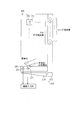
- FIG. 21 is a diagram showing a schematic configuration of the liquid crystal display device described in Patent Document 1.
- FIG. 21 is a diagram showing a schematic configuration of the liquid crystal display device described in Patent Document 1.
- the liquid crystal display device described in Patent Document 1 is used when the ambient light is blocked by a detection object such as a finger or when a non-visible light source is incident on the liquid crystal panel 220 from the backlight 210.
- the position (coordinates) of the detection target is detected by detecting the distribution of the amount of received light caused by light shielding or reflection by the detection target with the light receiving element 221 built in the liquid crystal panel 220 in a matrix.
- the backlight 210 includes a light source unit 213 and a light guide plate 214.
- the light source unit 213 includes red light as a non-visible light source 211 in addition to a visible light source 211 formed of a white LED (Light-Emitting-Diode).
- An infrared light source 212 composed of an outer LED is provided.
- the light receiving element 221 is arranged at a ratio of one or more elements (pixels) 222.
- Japanese Patent Publication Japanese Patent Laid-Open No. 2008-3296 (published on January 10, 2008)”
- the infrared light source 212 is disposed on the opposite side of the image display surface of the liquid crystal panel 220, and infrared light is incident on the image display region from the back side of the liquid crystal panel 220.
- the intensity (IR intensity) of infrared light in the image display region decreases, and the amount of light (the amount of received light) that reaches the light receiving element 221 after reflecting off the detection target. Get smaller. Therefore, it is difficult to accurately specify the position of the detection target.
- the IR intensity decreases as the distance L from the image display surface to the detection target increases.
- the IR intensity is 1070 ⁇ W
- the IR intensity is 1070 ⁇ W
- the intensity drops to 665 ⁇ W.
- the present invention has been made in view of the above problems, and an object of the present invention is to provide a display device that can accurately identify the position of a detection target even when the detection target and the display panel are separated from each other. It is to provide.
- a display device provides A display device having a function of identifying the position of the detection target in the image display region by making light incident on the image display region of the display panel and detecting the light reflected by the detection target, A first light emitting unit and a second light emitting unit for irradiating the image display area with light;
- the first light emitting unit is disposed on the side opposite to the image display surface of the display panel, and allows light to enter the image display region from the back side of the display panel,
- the second light emitting unit is disposed outside the image display area and makes light incident on the image display area without passing through the display panel.
- the first light emitting unit includes a light source for displaying an image and a first light source that causes light to enter the image display region in order to specify the position of the detection target. You can also.
- the second light emitting unit may include one or more second light sources that allow light to enter the image display area in order to specify the position of the detection target.
- the second light emitting unit includes a plurality of the second light sources, Each 2nd light source can also be set as the structure provided in each corner
- each second light source may be configured such that light emitted from the second light source crosses over the image display area.
- the second light emitting unit further includes a light guide member outside the image display region,
- the second light source makes light incident on the light guide member,
- the light guide member may be configured to cause light incident from the second light source to enter the image display region from an exit surface of the light guide member.
- the light guide member may be provided along each side of the image display area so as to surround the image display area.
- the light emitted from the second light emitting unit propagates through the inside of the light guide member, is emitted from the exit surface of the light guide member, and enters the image display region.
- the light guide member is provided along each side of the image display area so as to surround the image display area. Therefore, since uniform light can be incident on the image display area from the periphery of the image display area, the detection object is positioned regardless of the horizontal position (position in the XY plane parallel to the image display surface). More accurate position can be specified.
- the first light source is preferably an infrared light source that emits infrared light.
- the second light source is preferably an infrared light source that emits infrared light.
- infrared light is transmitted through the display panel regardless of the image display state (visible light transmittance), it is possible to avoid the problem that the amount of light for position detection is insufficient when the display screen is dark.
- the display panel may be configured to display a stereoscopic image.
- the position of the detection target (such as a finger of the user of the display device) can be accurately specified even in a region away from the image display surface of the display panel.
- the position of the detection object (finger or input pen) when the instruction is given can be accurately specified as intended by the user.
- the display panel may be configured to switch between a first display mode for displaying a planar image and a second display mode for displaying a stereoscopic image.
- the position of the object can be specified.
- the display device includes the first light emitting unit and the second light emitting unit that irradiate the image display region with light, and the first light emitting unit is opposite to the image display surface of the display panel.
- the second light emitting unit is disposed outside the image display area and does not go through the display panel and enters the image display area. In this configuration, light is incident. Therefore, the position of the detection target can be accurately specified even when the detection target and the display panel are separated from each other.
- An example of the relationship between the distance L from the image display surface of the liquid crystal panel in the present liquid crystal display device and the IR intensity of the infrared light when the optical sensor receives the infrared light (reflected light) reflected from the detection target It is a graph which shows. It is a graph which shows the measurement result of the IR intensity of the reflected light in the structure (structure of this liquid crystal display device) which used the 1st infrared light source and the 2nd infrared light source together in the graph shown in FIG. It is a block diagram which shows schematic structure of this liquid crystal display device. It is a circuit block diagram which shows the circuit structure of the liquid crystal panel in this liquid crystal display device, and one structural example of the peripheral circuit.
- FIG. 1 is a schematic diagram which shows the specific example of the arrangement state of an optical sensor.
- 3 is a timing chart showing the operation of the present liquid crystal display device. It is a flowchart which shows the example of the process which pinpoints the position where the reflected light of the detection target object was irradiated in this liquid crystal display device.
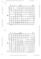
- (A) is a schematic diagram of a scanned image when reflected light is irradiated to one pixel
- (b) is a schematic diagram of a scanned image when reflected light is irradiated to a plurality of pixels.
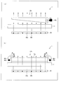
- FIG. It is a top view which shows the other structure of this liquid crystal display device.
- 14A is a cross-sectional view taken along the line AB of FIG. 14, and FIG.
- FIG. 14B is a view taken along the arrow C in FIG.
- FIG. 15 is a plan view schematically showing how light travels in the liquid crystal display device shown in FIG. 14. It is a top view which shows other structure of this liquid crystal display device.
- (A) is a sectional view taken along the line DE in FIG. 17, and (b) is a view taken in the direction of arrow F in FIG.
- FIG. 18 is a plan view schematically showing how light travels in the liquid crystal display device shown in FIG. 17.
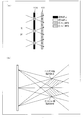
- the principle of 3D display in the liquid crystal display device using a parallax barrier is shown, (a) shows the provision effect of the viewing angle by a parallax barrier, (b) has shown the observation area
- FIG. An example of the relationship between the distance L from the image display surface of the display panel in the conventional display device and the IR intensity of the infrared light when the optical sensor receives the infrared light (reflected light) reflected from the detection target It is a graph which shows.
- a touch panel function is provided as an example of a display device having a function of specifying (detecting) the position (coordinates) of a detection target (such as a finger of the display device user or an input pen) in the image display area.
- a detection target such as a finger of the display device user or an input pen
- a liquid crystal display device (hereinafter referred to as a liquid crystal display device) provided will be described.
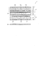
- FIG. 1 is a cross-sectional view showing a schematic configuration of a liquid crystal display device according to the present embodiment
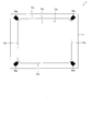
- FIG. 2 is a plan view showing a schematic configuration of the liquid crystal display device according to the present embodiment
- FIG. 3 is a cross-sectional view showing partial details of the liquid crystal panel in the liquid crystal display device shown in FIG.
- the liquid crystal display device 1 includes a liquid crystal panel 10 (display panel), a backlight 30 (first light emitting unit), and a front light emitting unit 40 (second light emitting). Part).
- the front light emitting unit 40 is omitted for convenience of explanation.
- the backlight 30 is an illumination device that irradiates light to the liquid crystal panel 10 and is provided on the back side of the liquid crystal panel 10.
- the backlight 30 includes a visible light source 30a for image display and a light source 30b (first light source) for detecting the position (coordinates) of the detection target.
- the light source 30b is not included in the backlight 30, and may be separately provided on the back side of the liquid crystal panel 10.
- infrared light visible light, ultraviolet light or the like can be used.
- infrared light is transmitted (passed) through the liquid crystal panel 10 regardless of the image display state (visible light transmittance)
- the problem of insufficient light amount for position detection when the display screen is dark is avoided. be able to.
- infrared light is used as the position detection light
- the light source 30b will be described as the first infrared light source 30b.
- the liquid crystal panel 10 includes an active matrix substrate 11 (TFT substrate), a counter substrate 12 (color filter (CF) substrate), a liquid crystal layer 13, polarizing plates 14a and 14b, and a protective plate (not shown). Pixels for displaying an image are arranged in a matrix.
- the active matrix substrate 11 and the counter substrate 12 are arranged to face each other with the liquid crystal layer 13 interposed therebetween.
- a polarizing plate 14 a is provided on the image display side (front side) of the counter substrate 12, and a polarizing plate 14 b is provided on the side (back side) opposite to the image display side of the active matrix substrate 11.
- Each polarizing plate 14a, 14b serves as a polarizer.
- the polarization direction of the front-side polarizing plate 14a and the polarization direction of the back-side polarizing plate 14b are arranged so as to have a crossed Nicols relationship.
- a normally black mode liquid crystal panel 10 can be realized.
- the active matrix substrate 11 includes a TFT (not shown) serving as a switching element for driving each pixel, an alignment film 16, an optical sensor 17 (light receiving element), a pixel electrode 23, and a data signal line on a glass substrate 15. 24 etc. are provided.
- the optical sensor 17 is composed of a photodiode, a phototransistor, or the like, and calculates the amount of received light by taking out a current or charge according to the intensity of the received light to the outside.
- an optical sensor made of a-Si (amorphous silicon), p-Si (polysilicon, polycrystalline silicon) or CG silicon (Continuous Grain Silicon) can be used.
- a color filter layer 19 In the counter substrate 12, a color filter layer 19, a counter electrode 20, an alignment film 21 and the like are formed on a glass substrate 18.
- the color filter layer 19 includes a colored portion having each color of red (R) (19r), green (G) (19g), and blue (B) (19b), and a black matrix 22.
- the front light emitting unit 40 includes four bullet-type light sources 40a (second light sources), and each light source 40a is arranged around the image display region 12b on the side surface 12a of the counter substrate 12, as shown in FIGS. It is provided at each corner (four corners) of (outer side).
- the number of light sources 40a is not particularly limited, and at least one light source 40a may be provided, and the shape of the light sources 40a is not limited to the bullet type.
- infrared light infrared light, visible light, ultraviolet light, or the like can be used, but it is preferable to use infrared light as with the light source 30b.
- infrared light is used as the light of the light source 40a
- the light source 40a will be described as the second infrared light source 40a.
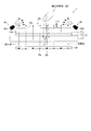
- FIG. 4 shows light emitted from the backlight 30 (light emitted from the visible light source 30a and the first infrared light source 30b (first infrared light)) and emitted from the second infrared light source 40a of the front light emitting unit 40.
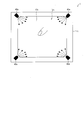
- FIG. 5 is a cross-sectional view schematically showing the progress of the emitted light, and FIG. 5 schematically shows the progress of the light emitted from the second infrared light source 40a when the image display region 12b is viewed in plan.
- FIG. 4 and 5 the broken line indicates visible light (light emitted from the visible light source 30a), and the solid line indicates infrared light.
- Each of the second infrared light sources 40a passes on a straight line in which the optical axis of the infrared light (second infrared light) emitted from each of the second infrared light sources 40a is perpendicular to the liquid crystal panel 10 and passes through the center of the image display region 12b.
- the angle of the light exit surface of the light source is set so as to cross over the image display area 12b (detection target side).
- FIG. 4 shows a case where the emission angle of the optical axis of the second infrared light is set to 45 degrees with respect to the image display surface 10a.
- the emission angle is not particularly limited, and is appropriately set according to the size and shape of the liquid crystal panel 10 and the number of second infrared light sources 40a.
- the infrared light (second infrared light) emitted from the second infrared light source 40a is the same as the infrared light (first infrared light) emitted from the first infrared light source 30b.
- the light is incident on the image display area 12b without passing through the liquid crystal panel 10.
- the intensity of the infrared light incident on the image display region 12b is higher than the intensity of the first infrared light. growing.
- region (irradiation range) of infrared light can be extended in the direction away from the image display surface 10a.
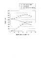
- FIG. 6 is a graph showing an example of the relationship between the distance L from the image display surface 10a of the liquid crystal panel 10 and the IR intensity of infrared light at the distance L.
- the IR intensity measurement result when only the first infrared light source 30b is provided see FIG. 22 as in the conventional configuration
- the case where only the second infrared light source 40a is provided image display
- the measurement results of the IR intensity in the case of being provided at the four corners around the region 12b are shown in comparison.
- the second infrared light is more IR-irradiated than the first infrared light. It can be seen that the strength increases. That is, it can be seen that when the second infrared light source 40a is provided, the infrared light arrival area (irradiation range) extends in a direction away from the image display surface 10a.
- the irradiation range of the second infrared light is not included, and therefore the first infrared light is more than the second infrared light. Increases the IR intensity.
- the magnitude relationship between the IR intensities of the first infrared light and the second infrared light is reversed with the position where the distance from the image display surface 10a to the detection target is 35 mm as a heel. This boundary point fluctuates by adjusting the angle of the emission direction of the second infrared light source 40a.
- the example of this graph shows a case where the emission angle of the optical axis of the second infrared light emitted from the second infrared light source 40a is set to be 45 degrees with respect to the image display surface 10a.
- the first infrared light source 30b and the second infrared light source 40a are used in combination.
- the second infrared light is irradiated to a region where the IR intensity of the first infrared light is low, and the irradiation range is compensated for each other. Therefore, a sufficient IR intensity can be obtained regardless of the distance L from the image display surface 10a to the detection target.
- FIG. 7 shows a measurement result of IR intensity in the liquid crystal display device 1 in which the first infrared light source 30b and the second infrared light source 40a are used in combination with the graph shown in FIG.
- the IR intensity of the infrared light in the image display region 12b is a value obtained by adding the IR intensity of the first infrared light and the IR intensity of the second infrared light.
- sufficient IR intensity is obtained in both the region where the distance L from the image display surface 10a to the detection target is small and the region where the distance is large.
- the IR intensity is greatest when the distance L is around 40 mm.
- FIG. 8 is a block diagram showing a schematic configuration of the liquid crystal display device 1.
- the liquid crystal display device 1 includes a liquid crystal panel 10, a backlight 30, a panel drive circuit 31, a white LED drive circuit 32, an infrared LED drive circuit 33, an A / D converter 36, an image processing unit 35, an illuminance sensor 37, and A microprocessor unit (hereinafter referred to as MPU) 38 is provided.
- MPU microprocessor unit
- the liquid crystal panel 10 includes a plurality of pixels and a plurality of photosensors 17 arranged in a matrix (see FIGS. 1 to 3).
- Display data Din is input to the liquid crystal display device 1 from an external device (not shown).
- the input display data Din is supplied to the panel drive circuit 31 via the image processing unit 35.
- the panel drive circuit 31 supplies a voltage corresponding to the display data Din to each pixel of the liquid crystal panel 10. As a result, an image based on the display data Din is displayed on the liquid crystal panel 10 by each pixel.
- the backlight 30 includes a plurality of white LEDs (Light Emitting Diodes) 30a and a plurality of first infrared LEDs 30b, and irradiates light (white light and infrared light) to the back surface of the liquid crystal panel 10.
- the white LED drive circuit 32 switches whether to supply the power supply voltage to the white LED 30a according to the white LED control signal WC output from the MPU 38.
- the white LED drive circuit 32 supplies a power supply voltage when the white LED control signal WC is at a high level and does not supply a power supply voltage when the white LED control signal WC is at a low level.
- the white LED 30a is turned on while the white LED control signal WC is at a high level, and is turned off while the white LED control signal WC is at a low level.
- the infrared LED drive circuit 33 supplies power supply voltage to the first infrared LED 30b of the backlight 30 and the second infrared LED 40a of the front light emitting unit 40 according to the IR control signal IRC output from the MPU 38. Switch.
- the infrared LED drive circuit 33 supplies a power supply voltage when the IR control signal IRC is at a high level and does not supply a power supply voltage when the IR control signal IRC is at a low level.
- the first infrared LED 30b and the second infrared LED 40a are turned on while the IR control signal IRC is at a high level, and are turned off while the IR control signal IRC is at a low level.
- the first infrared LED 30b and the second infrared LED 40a are turned on or off at the same timing based on the IR control signal IRC.
- the liquid crystal panel 10 outputs the output signal of the optical sensor 17 as the sensor output signal SS.
- the A / D converter 36 converts the analog sensor output signal SS into a digital signal.
- the output signal of the A / D converter 36 is a signal representing the position specified by the infrared light reflected from the detection target.
- MPU38 performs the process which pinpoints the position of a detection target based on sensor output signal SS acquired in the sensing period of coordinate information. Then, the MPU 38 performs a coordinate determination process based on the result of the position specifying process, determines the coordinates in the image corresponding to the position irradiated by the reflected light from the detection target, and outputs the determined coordinates as coordinate data. To do.
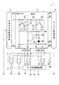
- FIG. 9 is a circuit block diagram showing a circuit configuration of the liquid crystal panel 10 and one configuration example of its peripheral circuits.
- One pixel is assumed to be composed of three picture elements corresponding to colors. That is, as shown in FIG. 9, the pixel P includes a red picture element 40r corresponding to red (R), a green picture element 40g corresponding to green (G), and a blue picture element 40b corresponding to blue (B). Is done.
- the optical sensor 17b is arranged so that the photodiode 39b is located in the same column as the blue picture element 40b. That is, the optical sensor 17b is arranged so that the photodiode 39b is positioned on the back surface of the blue filter (see FIGS. 3 and 9).
- the optical sensor 17 is arranged so that the photodiode 39r is positioned on the back surface of the red filter.
- the optical sensors 17b of the blue picture elements 40b and the optical sensors 17r of the red picture elements 40r are regularly arranged in an approximately equal number.
- FIG. 10A is a schematic diagram illustrating an example of an arrangement state of the optical sensors 17 in this case.
- “R”, “G”, and “B” indicate a red picture element, a green picture element, and a blue picture element, respectively, and “S” indicates an optical sensor.
- the photosensor “S” is arranged in the blue picture element “B”, and in the pixels Pb and Pd, the photosensor “S” is arranged in the red picture element “R”.
- the picture element in which the optical sensor “S” is arranged is different for each horizontal line, but the arrangement rule is not limited to this.
- the optical sensor “S” may be arranged in different picture elements for each vertical line.
- the optical sensor “S” may be arranged in a different picture element for each adjacent pixel.
- two optical sensors “S” may be provided in each pixel.
- the optical sensor “S” may be provided in each picture element.
- the optical sensor 17 is not limited to the configuration provided on the back surface of the filter corresponding to each picture element as shown in FIG. 3, FIG. 9 and FIG.
- the color filter layer 19 (see FIG. 3) facing the optical sensor 17 may be a filter that transmits only infrared light (infrared filter).
- the liquid crystal panel 10 includes m scanning signal lines G1 to Gm, 3n data signal lines SR1 to SRn, SG1 to SGn, SB1 to SBn, and (m ⁇ 3n) pixels P.
- the scanning signal lines G1 to Gm are arranged in parallel to each other, and the data signal lines SR1 to SRn, SG1 to SGn, and SB1 to SBn are arranged in parallel to each other so as to be orthogonal to the scanning signal lines G1 to Gm.
- the sensor readout lines RW1 to RWm and the sensor reset lines RS1 to RSm are arranged in parallel with the scanning signal lines G1 to Gm.
- One pixel P (40r, 40g, 40b) is provided near the intersection of the scanning signal lines G1 to Gm and the data signal lines SR1 to SRn, SG1 to SGn, and SB1 to SBn.
- the number of pixels P is m in the column direction (vertical direction in FIG. 9) and 3n in the row direction (horizontal direction in FIG. 9), and is arranged in a two-dimensional (matrix) shape as a whole.
- the pixel P is classified into the red picture element 40r, the green picture element 40g, and the blue picture element 40b according to the color of the color filter provided.
- the three types of picture elements 40r, 40g, and 40b are arranged side by side in the row direction, and three constitute one pixel.
- the pixel P includes a TFT (Thin Film Transistor) 51 and a liquid crystal capacitor 52.
- the gate terminal of the TFT 51 is connected to the scanning signal line Gi (i is an integer of 1 to m), and the source terminal is one of the data signal lines SRj, SGj, SBj (j is an integer of 1 to n).
- the drain terminal is connected to a pixel electrode (not shown), the pixel electrode is connected to one electrode of the liquid crystal capacitor 52, and the other electrode of the liquid crystal capacitor 52 is connected to the common electrode.
- the data signal lines SG1 to SGn connected to the green picture element 40g are referred to as G data signal lines
- the data signal lines SB1 to SBn connected to the blue picture element 40b are referred to as B data signal lines.
- the pixel P may include an auxiliary capacitor.
- the light transmittance (pixel brightness) of the pixel P is determined by the voltage written to the pixel P.
- a high level voltage TFT 32a is turned on on the scanning signal line Gi.
- Voltage to be written to the data signal line SXj By writing a voltage corresponding to the display data Din to the pixel P, the luminance of the picture element can be set to a desired level.
- the optical sensor 17 includes a capacitor 39a, a photodiode 39b, and a sensor preamplifier 39c.
- One electrode of the capacitor 39a is connected to the cathode terminal of the photodiode 39b (hereinafter, this connection point is referred to as a node A).
- the other electrode of the capacitor 39a is connected to the sensor readout line RWi, and the anode terminal of the photodiode 39b is connected to the sensor reset line RSi.
- the sensor preamplifier 39c includes a TFT having a gate terminal connected to the node A, a drain terminal connected to the B data signal line SBj, and a source terminal connected to the G data signal line SGj.
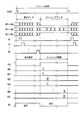
- a predetermined voltage is applied to the sensor readout line RWi and the sensor reset line RSi at the timing of the timing chart shown in FIG.
- the power supply voltage VDD may be applied to the B data signal line SBj.
- the power supply voltage VDD When the power supply voltage VDD is applied to the B data signal line SBj, the voltage at the node A is amplified by the sensor preamplifier 39c, and the amplified voltage is output to the G data signal line SGj. Therefore, the amount of light detected (received) by the optical sensor 17 can be obtained based on the voltage of the G data signal line SGj.
- a scanning signal line driving circuit 41 As shown in FIG. 9, at the periphery of the liquid crystal panel 10, there are a scanning signal line driving circuit 41, a data signal line driving circuit 42, a sensor row driving circuit 43, and p sensor outputs (p is an integer between 1 and n).
- An amplifier 44 and a plurality of switches 45 to 48 are provided.
- the scanning signal line drive circuit 41, the data signal line drive circuit 42, and the sensor row drive circuit 43 correspond to the panel drive circuit 31 in FIG.
- the data signal line driving circuit 42 has 3n output terminals corresponding to 3n data signal lines.
- One switch 45 is provided between each of the G data signal lines SG1 to SGn and n output terminals corresponding thereto, and the B data signal lines SB1 to SBn and n output terminals corresponding thereto are connected.
- One switch 46 is provided between them.
- the G data signal lines SG1 to SGn are divided into p groups, and the kth (k is an integer of 1 to p) G data signal lines and the input terminals of the kth sensor output amplifier 44 in the group.
- One switch 47 is provided between each switch.
- the B data signal lines SB1 to SBn are all connected to one end of the switch 48, and the power supply voltage VDD is applied to the other end of the switch 48.
- the number of switches 45 to 47 included in FIG. 9 is n, and the number of switches 48 is one.
- the liquid crystal display device 1 performs different operations in the display period and the sensing period.
- the switches 45 and 46 are turned on, and the switches 47 and 48 are turned off.
- the switches 45 and 46 are turned off, the switch 48 is turned on, and the switch 47 is connected to the input terminals of the sensor output amplifier 44 in order of the G data signal lines SG1 to SGn for each group. Thus, it is turned on in time division.
- the scanning signal line drive circuit 41 and the data signal line drive circuit 42 operate.
- the scanning signal line drive circuit 41 selects one scanning signal line for each line time from the scanning signal lines G1 to Gm in accordance with the timing control signal C1 (see FIG. 9). A high level voltage is applied, and a low level voltage is applied to the remaining scanning signal lines.
- the data signal line driving circuit 42 drives the data signal lines SR1 to SRn, SG1 to SGn, and SB1 to SBn in a line sequential manner based on the display data DR, DG, and DB output from the image processing unit 35.
- the data signal line drive circuit 42 stores the display data DR, DG, and DB for at least one row, and applies a voltage corresponding to the display data for one row for each line time to the data signal lines SR1 to SR1. Applied to SRn, SG1 to SGn, and SB1 to SBn. Note that the data signal line driving circuit 42 may drive the data signal lines SR1 to SRn, SG1 to SGn, and SB1 to SBn in a dot sequential manner.
- the sensor row driving circuit 43 and the sensor output amplifier 44 operate.
- the sensor row driving circuit 43 selects one signal line from the sensor readout lines RW1 to RWm and the sensor reset lines RS1 to RSm for each one line time.
- a predetermined readout voltage and reset voltage are applied to the sensor readout line and sensor reset line, and voltages different from those at the time of selection are applied to the other signal lines.
- the length of one line time differs between the display period and the sensing period.
- the sensor output amplifier 44 amplifies the voltage selected by the switch 47 and outputs it as sensor output signals SS1 to SSp.
- the white LED control signal WC is at a high level during the display period and is at a low level during the sensing period.
- the white LED 30a (see FIG. 8) of the backlight 30 is turned on during the display period and is turned off during the sensing period. For this reason, the influence of the backlight light on the photodiode 39b can be reduced.
- the IR control signal IRC becomes low level during the display period and becomes high level during the sensing period.
- the first infrared LED 30b of the backlight 30 and the second infrared LED 40a (see FIG. 8) of the front light emitting unit 40 are turned off during the display period and turned on during the sensing period. For this reason, the influence of white light (visible light) on the photodiode 39b can be reduced.
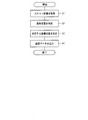
- FIG. 12 is a flowchart showing an example of processing for specifying the position of the liquid crystal display device 1 irradiated with the reflected light of the detection target. The process shown in FIG. 12 is performed within one frame time by the MPU 38 shown in FIG.
- the A / D converter 36 (see FIG. 8) converts the analog output signal SS output from the optical sensor 17 built in the liquid crystal panel 10 into a digital signal. For example, when position detection is performed using reflected light reflected from the detection target, the output signal SS from the optical sensor 17 arranged in association with the blue picture element is converted into a digital signal.
- the MPU 38 acquires this digital signal as a scanned image (step S1). Further, the MPU 38 performs a process for specifying the pixel position on the acquired scan image (step S2).
- FIG. 13A is a schematic diagram of a scanned image having the number of pixels of m ⁇ n.
- a pixel having a value of “1” is determined to be a pixel irradiated with reflected light, and Such a pixel position is specified.
- the pixel position (Xn-i, Ym-j) is specified.
- FIG. 13B shows a scan image when the reflected light is irradiated to a plurality of pixels because the irradiation range of the reflected light is large.
- the pixel position specified in this case includes eight pixels around the pixel position (Xn-i, Ym-j). It should be noted that the scan image in the figure is acquired in the case of the arrangement rule shown in FIG. 10D or E.
- the MPU 38 performs a process of determining the coordinate position in the image corresponding to the specified pixel (step S3). For example, as shown in FIG. 13A, coordinates corresponding to the specified pixel position (Xn-i, Ym-j) are determined. When the image resolution of the display image and the screen resolution of the liquid crystal panel match with “m ⁇ n”, the pixel position (Xn ⁇ i, Ym ⁇ j) is determined as the coordinate position. If the image resolution and the screen resolution do not match, coordinate conversion may be performed to determine the coordinate position corresponding to the pixel position.
- the coordinate position is determined based on a predetermined rule. That's fine.
- the coordinate position may be determined based on the pixel closest to the specified pixel's center of gravity.
- the corresponding coordinates can be determined based on the pixel position (Xn-i, Ym-j) corresponding to the center of gravity of the plurality of pixels having the value "1". .
- coordinates corresponding to all pixel positions having a value of “1” may be determined as coordinate positions.
- FIG. 1 and FIG. 2 the second infrared light source 40a of the front light emitting unit 40 is provided at each corner (four corners) around the image display region 12b on the side surface 12a of the counter substrate 12.
- the front light emission part 40 which concerns on this form is not limited to this, It is good also as a structure shown to (a) (b) of FIG. 14 and FIG. 14 is a plan view showing another configuration of the liquid crystal display device 1.
- FIG. 15 (a) is a view taken along arrow C in FIG. 14, and FIG. 15 (b) is a cross-sectional view taken along line AB in FIG. FIG.
- the front light emitting unit 40 includes a light guide 40c (light guide member) in addition to the second infrared light source 40a.
- a light guide 40c light guide member
- one second infrared light source 40a is provided at the center of each side surface 12a of the counter substrate 12, and one end surface of the light guide 40c is emitted from the second infrared light source 40a. While facing the surface, an end portion having the other end surface is provided so as to surround the periphery of the counter substrate 12.
- the exit surface of the light guide 40c is set, for example, such that the optical axis of the emitted light is 45 degrees from the image display surface 10a.
- emitted from the 2nd infrared light source 40a propagates the inside of the light guide 40c, is radiate
- FIG. 16 shows how light travels in the liquid crystal display device 1 having the above-described configuration. As shown in this figure, since uniform infrared light can be incident on the image display area 12b from the periphery of the counter substrate 12, the position of the detection target in the horizontal direction (X ⁇ parallel to the image display surface 10a). A more accurate position can be specified regardless of the position in the Y plane.
- the shape of the light guide 40c shown in FIGS. 14 and 15 is not particularly limited.
- the shape shown in FIGS. 17 and 18 (a) and 18 (b) may be used as another configuration.
- 17 is a plan view showing another configuration of the liquid crystal display device 1.
- FIG. 18A is a view taken in the direction of the arrow F in FIG. 17, and
- FIG. 18B is a cross-sectional view taken along the line DE in FIG. FIG.
- the second infrared light source 40a is provided at each corner (four corners) around the image display region 12b and is incident from the incident end (side surface) of each light guide 40c, as in FIGS.
- the reflected infrared light is reflected and propagated inside, and is incident on the image display region 12b from the exit surface (upper surface).
- each configuration described above four second infrared light sources 40a are provided.
- one second infrared light source 40a may be provided.
- infrared light emitted from one second infrared light source 40a is applied to a light guide 40c integrally formed so as to surround the periphery of the image display region 12b.
- the incident light is propagated while being repeatedly reflected inside the light guide 40c, and can be made incident on the image display region 12b from the exit surfaces of the four sides of the light guide 40c.
- the liquid crystal display device 1 is not limited to a configuration for displaying a planar image (2D: Two-Dimension), and may be a configuration for displaying a stereoscopic image (3D: Three-Dimension). .
- an image for the left eye and an image for the right eye on the display screen for example, color, polarization state, or display time
- a spectacle-like filter system worn by an observer in order to supply images of different viewpoints to the left and right eyes of an observer, an image for the left eye and an image for the right eye on the display screen, for example, color, polarization state, or display time
- a spectacle-like filter system worn by an observer in order to supply images of different viewpoints to the left and right eyes of an observer, an image for the left eye and an image for the right eye on the display screen, for example, color, polarization state, or display time
- the liquid crystal panel of the liquid crystal display device is combined with a parallax barrier in which a light transmission region and a light blocking region are formed in stripes, so that a 3D image can be obtained without using a visual aid such as a filter system on the viewer side.
- a recognized configuration may be used.
- 20A and 20B show the principle of 3D display in a liquid crystal display device using a parallax barrier, where FIG. 20A shows the effect of providing a viewing angle by the parallax barrier, and FIG. 20B shows the observation area of the 3D display screen. ing.
- a specific viewing angle is given to the right-eye image and the left-eye image generated by the liquid crystal panel 101 by the parallax barrier 102 (see FIG. 20A), and a specific space-specific image is obtained. Only an image corresponding to each eye is visually recognized from the observation area, so that a 3D image is recognized by the observer (see FIG. 20B).
- the liquid crystal display device 1 can be configured to have a function of switching between flat display (2D) (first display mode) and stereoscopic display (3D) (second display mode).
- 2D flat display
- 3D stereoscopic display
- 3D display and 2D display can be realized by electrically switching between and. That is, in this liquid crystal display device, 3D display is performed when the parallax barrier effect is enabled by turning on / off the switching liquid crystal layer, and 2D display is performed when the parallax barrier effect is disabled.
- the configuration for performing 2D display and 3D display is not particularly limited, and a well-known technique can be employed.
- the position of the detection target (such as a finger of the user of the liquid crystal display device) can be accurately specified even in a region away from the image display surface 10 a of the liquid crystal panel 10.
- the position of the finger when giving an instruction to the 3D image recognized by the user can be accurately specified as intended by the user. Therefore, the liquid crystal display device 1 is suitable for a configuration that performs 3D display.
- the present liquid crystal display device may display different images in different directions, specifically, so-called dual view display, bail view display, and triple view display.
- a liquid crystal display device has been described as an example of a display device.
- the present embodiment is not limited to this, and is an electroluminescence (EL) display device. May be.
- the present invention can be suitably used for a 3D display device with a touch panel with a built-in optical sensor.
- Liquid crystal display device 10 Liquid crystal panel (display panel) 10a Image display surface 11 Active matrix substrate (TFT substrate) 12 Counter substrate (color filter (CF) substrate) 12a (opposite substrate) side surface 12b image display region 13 liquid crystal layer 14a (front side) polarizing plate 14b (back side) polarizing plate 15 (TFT substrate side) glass substrate 16 (TFT substrate side) orientation film 17 photosensor ( Light receiving element) 18 Glass substrate (on the CF substrate side) 19 Color filter layer 20 Counter electrode 21 Alignment film (on the CF substrate side) 22 Black matrix 23 Pixel electrode 24 Data signal line 30 Backlight (first light emitting unit) 30a Visible light source, white LED 30b 1st infrared light source, 1st infrared LED (1st light source) 31 Panel Drive Circuit 32 White LED Drive Circuit 33 Infrared LED Drive Circuit 35 Image Processing Unit 36 A / D Converter 37 Illuminance Sensor 38 Microprocessor Unit (MPU) 39a Capacitor 39b Photodiode 39c Sensor
Landscapes
- Physics & Mathematics (AREA)
- Engineering & Computer Science (AREA)
- General Physics & Mathematics (AREA)
- Theoretical Computer Science (AREA)
- Nonlinear Science (AREA)
- General Engineering & Computer Science (AREA)
- Optics & Photonics (AREA)
- Crystallography & Structural Chemistry (AREA)
- Chemical & Material Sciences (AREA)
- Mathematical Physics (AREA)
- Human Computer Interaction (AREA)
- Computer Hardware Design (AREA)
- Control Of Indicators Other Than Cathode Ray Tubes (AREA)
- Position Input By Displaying (AREA)
- Liquid Crystal (AREA)
Abstract
液晶パネル(10)の画像表示領域(12b)に光を入射して、検出対象物(指)に反射された光を検出することにより、画像表示領域(12b)における検出対象物(指)の位置を特定する機能を備えた液晶表示装置(1)であって、画像表示領域(12b)に光を照射するバックライト(30)およびフロント発光部(40)を備え、バックライト(30)は、液晶パネル(10)の画像表示面(10a)とは反対側に配置され、液晶パネル(10)の背面側から画像表示領域(12b)に光を入射させ、フロント発光部(40)は、画像表示領域(12b)の外側に配置され、液晶パネル(10)を介さずに画像表示領域(12b)に光を入射させる。これにより、検出対象物と表示パネルとが離間した状態でも、検出対象物の位置を正確に特定することができる表示装置を提供する。
Description
本発明は、表示パネルの画像表示領域に光を入射して、検出対象物に反射された光を検出することにより、上記画像表示領域における検出対象物の位置を特定する機能を備えた表示装置に関するものである。
液晶表示装置等の表示装置の中には、検出対象物(指や入力用のペン)でパネル表面を触れると、その触れた位置(座標)を検出することのできるタッチパネル機能を備えたタッチパネル付き表示装置が開発されている。
このようなタッチパネル付き表示装置(以下、表示装置と称す)としては、従来は、いわゆる抵抗膜方式や、静電容量式等のタッチパネルを用いた表示装置が主流に用いられていた。しかしながら、このような表示装置においては、例えば、位置検出用の特殊なパネルを必要とするため、装置全体が厚くなる。また、このようなタッチパネルを表示装置の画面(表示領域)に設けることによって、視認性が低下するという問題が生じる。
そこで、近年では、上記の抵抗膜方式や静電容量方式のタッチパネルに代えて、フォトダイオードやフォトトランジスタ等の受光素子(光センサ)を表示装置の画面内に内蔵した座標センサ一体型の表示装置の開発が進められている。
このような光学式の座標センサ一体型の表示装置は、例えば、特許文献1に記載されている。
図21は、特許文献1に記載されている液晶表示装置の概略構成を示す図である。
同図に示すように、特許文献1に記載されている液晶表示装置は、指等の検出対象物による環境光の遮光、あるいは、バックライト210から液晶パネル220に非可視光源を入射したときの検出対象物による遮光または反射によって生じる受光量の分布を、液晶パネル220にマトリクス状に内蔵された受光素子221で検出することにより、検出対象物の位置(座標)を検出する。なお、バックライト210は、光源部213と、導光板214とを有し、光源部213は、白色LED(Light Emitting Diode;発光ダイオード)からなる可視光源211の他に、非可視光源として、赤外LEDからなる赤外光源212を備えている。また、受光素子221は、1つまたは複数の素子(画素)222に対して1つの割合で配置されている。
しかしながら、上記液晶表示装置では、赤外光源212が液晶パネル220の画像表示面とは反対側に配置され、液晶パネル220の背面側から画像表示領域に赤外光を入射させているため、赤外光源212から検出対象物までの距離が大きくなると、画像表示領域における赤外光の強度(IR強度)が小さくなり、検出対象物に反射して受光素子221に到達する光量(受光量)が小さくなる。そのため、検出対象物の位置を正確に特定することが困難になる。
ここで、表示パネルの画像表示面から検出対象物までの距離Lと、距離Lにおける赤外光の強度(IR強度)との関係の一例を図22に示す。同図に示すように、画像表示面から検出対象物までの距離Lが大きくなるにつれて、IR強度は小さくなることが分かる。例えば、表示パネルの画像表示面から検出対象物までの距離Lが3mmのときは、IR強度が1070μWであるが、表示パネルの画像表示面から検出対象物までの距離Lが40mmになると、IR強度は665μWに低下する。このように、検出対象物を表示パネルに接触あるいは近接させる場合には、十分なIR強度を得られるため正確な位置を特定することができるが、検出対象物が表示パネルから遠ざかると、十分なIR強度を得られなくなるため、正確な位置を特定することが困難になる。
本発明は、上記の問題点に鑑みてなされたものであり、その目的は、検出対象物と表示パネルとが離間した状態でも、検出対象物の位置を正確に特定することができる表示装置を提供することにある。
本発明に係る表示装置は、上記課題を解決するために、
表示パネルの画像表示領域に光を入射して、検出対象物に反射された光を検出することにより、上記画像表示領域における検出対象物の位置を特定する機能を備えた表示装置であって、
上記画像表示領域に光を照射する、第1発光部および第2発光部を備え、
上記第1発光部は、上記表示パネルの画像表示面とは反対側に配置され、上記表示パネルの背面側から上記画像表示領域に光を入射させ、
上記第2発光部は、上記画像表示領域の外側に配置され、上記表示パネルを介さずに上記画像表示領域に光を入射させることを特徴とする。
表示パネルの画像表示領域に光を入射して、検出対象物に反射された光を検出することにより、上記画像表示領域における検出対象物の位置を特定する機能を備えた表示装置であって、
上記画像表示領域に光を照射する、第1発光部および第2発光部を備え、
上記第1発光部は、上記表示パネルの画像表示面とは反対側に配置され、上記表示パネルの背面側から上記画像表示領域に光を入射させ、
上記第2発光部は、上記画像表示領域の外側に配置され、上記表示パネルを介さずに上記画像表示領域に光を入射させることを特徴とする。
上記の構成では、第1発光部に加えて第2発光部から出射される光が、画像表示領域に入射される。また、第2発光部から入射される光は表示パネルを通過することなく画像表示領域に入射される。よって、画像表示領域における光の強度を、従来(図21、22参照)よりも大きくすることができる(図7参照)。これにより、画像表示面から検出対象物までの距離が小さい領域および大きい領域ともに、検出対象物から十分な強度の反射光(第1発光部の光の反射光および第2発光部の光の反射光)を得ることができる。よって、検出対象物と表示パネルとが離間した状態でも、検出対象物の位置を正確に特定することができる。
本表示装置では、上記第1発光部は、画像表示用の光源と、検出対象物の位置を特定するために上記画像表示領域に光を入射させる第1光源とを含んでいる構成とすることもできる。
本表示装置では、上記第2発光部は、検出対象物の位置を特定するために上記画像表示領域に光を入射させる第2光源を1つ以上含んでいる構成とすることもできる。
本表示装置では、上記第2発光部は、上記第2光源を複数備え、
各第2光源は、上記画像表示領域の周囲の各角部に設けられている構成とすることもできる。
各第2光源は、上記画像表示領域の周囲の各角部に設けられている構成とすることもできる。
本表示装置では、各第2光源は、該第2光源から出射される光が上記画像表示領域の上を横切るように設けられている構成とすることもできる。
本表示装置では、上記第2発光部は、上記画像表示領域の外側に導光部材をさらに備え、
上記第2光源は、上記導光部材に光を入射させ、
上記導光部材は、上記第2光源から入射された光を、該導光部材の出射面から上記画像表示領域に入射させる構成とすることもできる。
上記第2光源は、上記導光部材に光を入射させ、
上記導光部材は、上記第2光源から入射された光を、該導光部材の出射面から上記画像表示領域に入射させる構成とすることもできる。
本表示装置では、上記導光部材は、上記画像表示領域を取り囲むように、上記画像表示領域の各辺に沿って設けられている構成とすることもできる。
上記の構成では、第2発光部から出射された光は、導光部材の内部を伝播し、導光部材の出射面から出射され、画像表示領域に入射される。そして、導光部材は、画像表示領域を取り囲むように、画像表示領域の各辺に沿って設けられている。よって、画像表示領域の周囲から、画像表示領域に均一な光を入射することができるため、検出対象物の水平方向の位置(画像表示面に平行なX-Y平面内における位置)に関わらず、より正確な位置を特定することができる。
本表示装置では、上記第1光源は、赤外線を照射する赤外光源とすることが好ましい。
本表示装置では、上記第2光源は、赤外線を照射する赤外光源とすることが好ましい。
赤外光は、画像表示状態(可視光透過率)に関わらず表示パネルを透過するため、表示画面が暗い場合に位置検出のための光量が不足するという問題を回避することができる。
本表示装置では、上記表示パネルは、立体画像を表示する構成とすることもできる。
本表示装置では、表示パネルの画像表示面から離れた領域でも検出対象物(表示装置の使用者の指など)の位置を正確に特定することができるため、使用者が認識する立体画像に対して指示を与えたときの検出対象物(指や入力ペン)の位置を、使用者の意図したとおりに正確に特定することができる。
本表示装置では、上記表示パネルは、平面画像を表示する第1表示モードと、立体画像を表示する第2表示モードとを相互に切り替える構成とすることもできる。
本表示装置では、上記第1発光部および第2発光部から出射され上記検出対象物に反射された光を検出することにより、上記画像表示領域における上記表示パネルから離間した位置に存在する上記検出対象物の位置を特定することができる。
以上のように、本表示装置では、上記画像表示領域に光を照射する、第1発光部および第2発光部を備え、上記第1発光部は、上記表示パネルの画像表示面とは反対側に配置され、上記表示パネルの背面側から上記画像表示領域に光を入射させ、上記第2発光部は、上記画像表示領域の外側に配置され、上記表示パネルを介さずに上記画像表示領域に光を入射させる構成である。よって、検出対象物と表示パネルとが離間した状態でも、検出対象物の位置を正確に特定することができる。
本発明の実施の一形態について図面に基づいて説明すれば、以下の通りである。
本実施の形態では、画像表示領域における検出対象物(表示装置の使用者の指や入力ペンなど)の位置(座標)を特定(検出)する機能を備えた表示装置の一例として、タッチパネル機能を備えた液晶表示装置(以下、液晶表示装置と称す)について説明する。
図1は、本実施の形態に係る液晶表示装置の概略構成を示す断面図であり、図2は、本実施の形態に係る液晶表示装置の概略構成を示す平面図である。また、図3は、図1に示す液晶表示装置における液晶パネルの部分的な詳細を示す断面図である。
図1および図3に示すように、本実施の形態に係る液晶表示装置1は、液晶パネル10(表示パネル)と、バックライト30(第1発光部)と、フロント発光部40(第2発光部)とを備えている。なお、図3では、説明の便宜上、フロント発光部40を省略している。
バックライト30は、液晶パネル10に光を照射する照明装置であり、液晶パネル10の背面側に設けられている。バックライト30は、画像表示用の可視光源30aと、検出対象物の位置(座標)検出用の光源30b(第1光源)とを含んでいる。なお、光源30bはバックライト30に含まれず、液晶パネル10の背面側に別途設けられていても良い。
ここで、位置検出用の光としては、赤外光、可視光、紫外光等を用いることができる。しかしながら、赤外光は、画像表示状態(可視光透過率)に関わらず液晶パネル10を透過(通過)するため、表示画面が暗い場合に位置検出のための光量が不足するという問題を回避することができる。このため、液晶表示装置1における位置検出用の光としては、赤外光を用いることが好ましい。以下では、位置検出用の光として赤外光を用いた場合を例に挙げ、光源30bを第1赤外光源30bと称して説明する。
液晶パネル10は、アクティブマトリクス基板11(TFT基板)と、対向基板12(カラーフィルタ(CF)基板)と、液晶層13と、偏光板14a,14bと、保護板(図示せず)とを備え、画像を表示するための画素がマトリクス状に配されている。
アクティブマトリクス基板11および対向基板12は、液晶層13を介して対向配置されている。対向基板12における画像表示側(表側)には偏光板14aが設けられ、アクティブマトリクス基板11における画像表示側とは反対側(裏側)には偏光板14bが設けられている。
各偏光板14a,14bは、偏光子としての役割を果たす。例えば、液晶層13に封入されている液晶材料が垂直配向型である場合、表側の偏光板14aの偏光方向と裏側の偏光板14bの偏光方向とを、互いにクロスニコルの関係になるように配置することで、ノーマリーブラックモードの液晶パネル10を実現することができる。
アクティブマトリクス基板11には、ガラス基板15上に、各画素を駆動するためのスイッチング素子であるTFT(図示せず)、配向膜16、光センサ17(受光素子)、画素電極23、データ信号線24などが設けられている。
光センサ17は、フォトダイオードまたはフォトトランジスタ等で構成されており、受光した光の強度に応じた電流または電荷を外部に取り出すことによって、受光量を算出する。光センサ17は、例えば、a-Si(アモルファスシリコン)、p-Si(ポリシリコン、多結晶シリコン)あるいはCGシリコン(Continuous Grain Silicon;連続粒界結晶シリコン)からなる光センサを用いることができる。
対向基板12には、ガラス基板18上に、カラーフィルタ層19、対向電極20、配向膜21などが形成されている。カラーフィルタ層19は、赤(R)(19r)、緑(G)(19g)、青(B)(19b)のそれぞれの色を有する着色部と、ブラックマトリクス22とから構成されている。
フロント発光部40は4個の砲弾型の光源40a(第2光源)を含み、各光源40aは、図1、図2に示すように、対向基板12の側面12aにおける、画像表示領域12bの周囲(外側)の各角部(四隅)に設けられている。なお、光源40aの数は特に限定されるものではなく、少なくとも1つ設けられていればよく、また光源40aの形状も、砲弾型に限定されるものではない。
ここで、光源40aの光としては、赤外光、可視光、紫外光等を用いることができるが、光源30bと同様、赤外光を用いることが好ましい。以下では、光源40aの光として赤外光を用いた場合を例に挙げ、光源40aを、第2赤外光源40aと称して説明する。
次に、液晶表示装置1における光の進行の様子について説明する。図4は、バックライト30から出射された光(可視光源30aおよび第1赤外光源30bから出射された光(第1赤外光))およびフロント発光部40の第2赤外光源40aから出射された光の進行の様子を模式的示す断面図であり、図5は、画像表示領域12bを平面視した場合の、第2赤外光源40aから出射された光の進行の様子を模式的に示す平面図である。なお、図4および図5中の破線は可視光(可視光源30aから出射された光)を示し、実線は赤外光を示している。
各第2赤外光源40aは、それぞれから出射された赤外光(第2赤外光)の光軸が、液晶パネル10に垂直でかつ画像表示領域12bの中心を通る直線上を通過し、かつ画像表示領域12bの上(検出対象物側)を横切るように、光源の出射面の角度が設定されている。図4では、第2赤外光の光軸の出射角度を、画像表示面10aに対して45度に設定した場合を示している。なお、この出射角度は特に限定されるものではなく、液晶パネル10の大きさや形状、第2赤外光源40aの数などに応じて適宜設定される。
画像表示領域12bに入射された第1赤外光および第2赤外光のうち、検出対象物に反射された光の一部は、液晶パネル内の光センサ17に受光される。
上記の構成によれば、第2赤外光源40aから出射された赤外光(第2赤外光)は、第1赤外光源30bから出射された赤外光(第1赤外光)とは異なり、液晶パネル10を介さず(通過せず)に、画像表示領域12bに入射される。そのため、第2赤外光は、液晶パネル10内を伝播することによるIR強度の減衰が起こらないため、画像表示領域12bに入射される赤外光の強度は第1赤外光の強度よりも大きくなる。これにより、赤外光の到達領域(照射範囲)を、画像表示面10aから遠ざかる方向に広げることができる。
図6は、液晶パネル10の画像表示面10aからの距離Lと、距離Lにおける赤外光のIR強度との関係の一例を示すグラフである。なお、同図では、第1赤外光源30bのみを設けた場合(従来の構成と同様、図22参照)のIR強度の測定結果と、第2赤外光源40aのみを設けた場合(画像表示領域12bの周囲の四隅に設けた場合)のIR強度の測定結果とを比較して示している。同図に示すように、液晶パネル10の画像表示面10aから検出対象物までの距離Lが大きい領域(L>35mm)では、第1赤外光よりも第2赤外光の方が、IR強度が大きくなることが分かる。すなわち、第2赤外光源40aを設けた場合には、赤外光の到達領域(照射範囲)が、画像表示面10aから遠ざかる方向に広がることが分かる。
なお、画像表示面10aから検出対象物までの距離Lが小さい領域(L<35mm)では、第2赤外光の照射範囲を外れるため、第2赤外光よりも第1赤外光の方がIR強度が大きくなる。また、このグラフでは、画像表示面10aから検出対象物までの距離が35mmの位置を堺にして、第1赤外光および第2赤外光のIR強度の大小関係が逆転しているが、この境界点は、第2赤外光源40aの出射方向の角度調整により変動する。このグラフの例では、第2赤外光源40aから出射される第2赤外光の光軸の出射角度が、画像表示面10aに対して45度になるように設定した場合を示している。
本実施の形態に係る液晶表示装置1では、第1赤外光源30bおよび第2赤外光源40aを併用している。これにより、第1赤外光のIR強度が小さい領域に第2赤外光が照射され、互いに照射範囲を補償し合うことになる。そのため、画像表示面10aから検出対象物までの距離Lに関わらず、十分なIR強度を得ることができる。
図7には、図6に示すグラフに、さらに、第1赤外光源30bおよび第2赤外光源40aを併用した本液晶表示装置1におけるIR強度の測定結果を示している。同図に示すように、本液晶表示装置1では、画像表示領域12bにおける赤外光のIR強度は、第1赤外光のIR強度と第2赤外光のIR強度とを足し合わせた値になり、第1赤外光源30bのみ設けた場合(従来の構成と同様)と比較して、画像表示面10aから検出対象物までの距離Lが小さい領域および大きい領域ともに、十分なIR強度を得られることが分かる。この例では、特に、距離Lが40mm前後において、IR強度が最も大きくなることが分かる。これにより、検出対象物が、距離L=40mm付近に存在する場合であっても、検出対象物から強度の大きい反射光を得ることができるため、その位置を正確に特定することが可能となる。よって、検出対象物と液晶パネル10とが離間した状態でも、検出対象物の位置を正確に特定することができる。
次に、本実施の形態に係る液晶表示装置1の機能について説明する。
図8は、液晶表示装置1の概略構成を示すブロック図である。液晶表示装置1は、液晶パネル10、バックライト30、パネル駆動回路31、白色LED駆動回路32、赤外LED駆動回路33、A/D変換器36、画像処理部35、照度センサ37、および、マイクロプロセッサユニット(以下、MPUと称す)38を備えている。
液晶パネル10は、マトリクス状に配置された複数の画素と複数の光センサ17を含んでいる(図1~図3参照)。液晶表示装置1には、外部装置(図示せず)から表示データDinが入力される。入力された表示データDinは、画像処理部35を経由してパネル駆動回路31に供給される。パネル駆動回路31は、液晶パネル10の各画素に表示データDinに応じた電圧を供給する。これにより、液晶パネル10には表示データDinに基づく画像が各画素によって表示される。
バックライト30は、複数の白色LED(Light Emitting Diode)30aと複数の第1赤外LED30bとを含み、液晶パネル10の背面に光(白色光および赤外光)を照射する。白色LED駆動回路32は、MPU38から出力された白色LED制御信号WCに従い、白色LED30aに電源電圧を供給するか否かを切り替える。以下、白色LED駆動回路32は、白色LED制御信号WCがハイレベルのときは電源電圧を供給し、白色LED制御信号WCがローレベルのときは電源電圧を供給しないものとする。白色LED30aは、白色LED制御信号WCがハイレベルである間は点灯し、白色LED制御信号WCがローレベルである間は消灯する。
赤外LED駆動回路33は、MPU38から出力されたIR制御信号IRCに従い、バックライト30の第1赤外LED30b、および、フロント発光部40の第2赤外LED40aに電源電圧を供給するか否かを切り替える。以下、赤外LED駆動回路33は、IR制御信号IRCがハイレベルのときは電源電圧を供給し、IR制御信号IRCがローレベルのときは電源電圧を供給しないものとする。第1赤外LED30bおよび第2赤外LED40aは、IR制御信号IRCがハイレベルである間は点灯し、IR制御信号IRCがローレベルである間は消灯する。なお、第1赤外LED30bおよび第2赤外LED40aは、IR制御信号IRCに基づき、同一のタイミングで点灯あるいは消灯する。
液晶パネル10は、光センサ17の出力信号をセンサ出力信号SSとして出力する。A/D変換器36は、アナログのセンサ出力信号SSをデジタル信号に変換する。A/D変換器36の出力信号は、検出対象物から反射された赤外光によって特定された位置を表す信号である。MPU38は、座標情報のセンシング期間において取得したセンサ出力信号SSに基づいて、検出対象物の位置を特定する処理を行う。そして、MPU38は、位置特定処理の結果に基づいて座標決定処理を行い、検出対象物からの反射光により照射された位置に対応する画像内の座標を決定し、決定した座標を座標データとして出力する。
図9は、液晶パネル10の回路構成とその周辺回路の一構成例を示す回路ブロック図である。なお、1つの画素は、色に応じた3つの絵素で構成されているものとする。すなわち、図9に示すように、画素Pは、赤色(R)に対応する赤色絵素40r、緑色(G)に対応する緑色絵素40g、青色(B)に対応する青色絵素40bで構成される。光センサ17bは、フォトダイオード39bが青色絵素40bと同じ列に位置するように配置されている。すなわち、光センサ17bは、青色フィルタの背面にフォトダイオード39bが位置するように配置されている(図3、図9参照)。
図9に示す画素Pとは異なる画素(図示せず)においては、光センサ17は、赤色フィルタの背面にフォトダイオード39rが位置するように配置されている。そして、青色絵素40bの光センサ17bと、赤色絵素40rの光センサ17rは、ほぼ等しい数で規則的に配置されている。
図10の(a)は、この場合における光センサ17の配置状態の一例を示す模式図である。この図において、「R」、「G」、「B」は、それぞれ赤色絵素、緑色絵素、青色絵素を示しており、「S」は、光センサを示している。画素PaおよびPcにおいては、青色絵素「B」に光センサ「S」が配置され、画素PbおよびPdにおいては、赤色絵素「R」に光センサ「S」が配置されている。
なお、図10の(a)においては、水平ラインごとに、光センサ「S」を配置する絵素を異なるものとしたが、配置規則はこれに限定されない。例えば、図10の(b)に示すように、光センサ「S」は、垂直ラインごとに、異なる絵素に配置されてもよい。また、図10の(c)に示すように、光センサ「S」は、隣り合う画素ごとに、異なる絵素に配置されてもよい。また、図10の(d)に示すように、光センサ「S」は、各画素に2つ設けられてもよい。また、図10の(e)に示すように、光センサ「S」は、各絵素に設けられてもよい。
ここで、光センサ17は、図3、図9および図10に示したような、各絵素に対応するフィルタの背面に設けられる構成に限定されるものではない。光センサ17に対向するカラーフィルタ層19(図3参照)は、赤外光のみを透過するフィルタ(赤外フィルタ)であっても良い。
以下では、青色絵素40bと同じ列の青色フィルタの背面にフォトダイオード39bが位置するように配置された光センサ30bが、センサ出力信号を出力する動作の一例について説明する。
図9に示すように、液晶パネル10は、m本の走査信号線G1~Gm、3n本のデータ信号線SR1~SRn、SG1~SGn、SB1~SBnおよび、(m×3n)個の画素P(絵素40r、40g、40b)を備えるとともに、(m×n)個の光センサ17、m本のセンサ読み出し線RW1~RWmおよび、m本のセンサリセット線RS1~RSmを備える。
走査信号線G1~Gmは、互いに平行に配置され、データ信号線SR1~SRn、SG1~SGn、SB1~SBnは、走査信号線G1~Gmと直交するように互いに平行に配置される。センサ読み出し線RW1~RWmとセンサリセット線RS1~RSmは、走査信号線G1~Gmと平行に配置される。
画素P(40r、40g、40b)は、走査信号線G1~Gmとデータ信号線SR1~SRn、SG1~SGn、SB1~SBnの交差部近傍に1個ずつ設けられる。画素Pは、列方向(図9では縦方向)にm個ずつ、行方向(図9では横方向)に3n個ずつ、全体として2次元(マトリクス)状に配置される。
画素Pは、上述したように、設けられるカラーフィルタの色によって、赤色絵素40r、緑色絵素40gおよび青色絵素40bに分類される。3種類の絵素40r、40g、40bは、行方向に並べて配置され、3つで1つの画素を構成する。
画素Pは、TFT(Thin Film Transistor)51と液晶容量52を含んでいる。TFT51のゲート端子は走査信号線Gi(iは1以上m以下の整数)に接続されており、ソース端子はデータ信号線SRj、SGj、SBj(jは1以上n以下の整数)のいずれかに接続され、ドレイン端子は画素電極(図示せず)に接続され、画素電極が液晶容量52の一方の電極に接続され、液晶容量52の他方の電極が共通電極に接続される。以下、緑色絵素40gに接続されたデータ信号線SG1~SGnをGデータ信号線、青色絵素40bに接続されたデータ信号線SB1~SBnをBデータ信号線という。なお、画素Pは補助容量を含んでいてもよい。
画素Pの光透過率(絵素の輝度)は、画素Pに書き込まれた電圧によって定まる。走査信号線Giとデータ信号線SXj(XはR、G、Bのいずれか)に接続された画素Pにある電圧を書き込むためには、走査信号線Giにハイレベル電圧(TFT32aをオン状態にする電圧)を印加し、データ信号線SXjに書き込むべき電圧を印加すればよい。表示データDinに応じた電圧を画素Pに書き込むことにより、絵素の輝度を所望のレベルに設定することができる。
光センサ17は、コンデンサ39a、フォトダイオード39bおよびセンサプリアンプ39cにより構成される。
コンデンサ39aの一方の電極は、フォトダイオード39bのカソード端子に接続される(以下、この接続点を節点Aという)。コンデンサ39aの他方の電極はセンサ読み出し線RWiに接続され、フォトダイオード39bのアノード端子はセンサリセット線RSiに接続される。センサプリアンプ39cは、ゲート端子が節点Aに接続され、ドレイン端子がBデータ信号線SBjに接続され、ソース端子がGデータ信号線SGjに接続されたTFTで構成される。
センサ読み出し線RWiやBデータ信号線SBjなどに接続された光センサ17により光量を検出するためには、図11に示すタイミングチャートのタイミングで、センサ読み出し線RWiとセンサリセット線RSiに所定の電圧を印加し、Bデータ信号線SBjに電源電圧VDDを印加すればよい。具体的には、センサ読み出し線RWiとセンサリセット線RSiに所定の電圧を印加した後、フォトダイオード39bに光が入射すると、入射光量に応じた電流がフォトダイオード39bに流れ、節点Aの電圧は流れた電流の分だけ低下する。Bデータ信号線SBjに電源電圧VDDを印加すると、節点Aの電圧はセンサプリアンプ39cで増幅され、Gデータ信号線SGjには増幅後の電圧が出力される。したがって、Gデータ信号線SGjの電圧に基づき、光センサ17で検知(受光)された光量を求めることができる。
図9に示すように、液晶パネル10の周辺には、走査信号線駆動回路41、データ信号線駆動回路42、センサ行駆動回路43、p個(pは1以上n以下の整数)のセンサ出力アンプ44および、複数のスイッチ45~48が設けられる。走査信号線駆動回路41、データ信号線駆動回路42およびセンサ行駆動回路43は、図8のパネル駆動回路31に相当する。
データ信号線駆動回路42は、3n本のデータ信号線に対応して3n個の出力端子を有する。Gデータ信号線SG1~SGnとこれに対応したn個の出力端子との間にはスイッチ45が1個ずつ設けられ、Bデータ信号線SB1~SBnとこれに対応したn個の出力端子との間にはスイッチ46が1個ずつ設けられる。Gデータ信号線SG1~SGnはp本ずつのグループに分けられ、グループ内でk番目(kは1以上p以下の整数)のGデータ信号線とk番目のセンサ出力アンプ44の入力端子との間にはスイッチ47が1個ずつ設けられる。Bデータ信号線SB1~SBnは、いずれもスイッチ48の一端に接続され、スイッチ48の他端には電源電圧VDDが印加される。図9に含まれるスイッチ45~47の個数はn個であり、スイッチ48の個数は1個である。
本液晶表示装置1では、表示期間とセンシング期間で異なる動作を行う。表示期間では、スイッチ45、46はオン状態、スイッチ47、48はオフ状態となる。これに対して、センシング期間では、スイッチ45、46はオフ状態、スイッチ48はオン状態となり、スイッチ47はGデータ信号線SG1~SGnがグループごとに順にセンサ出力アンプ44の入力端子に接続されるように時分割でオン状態となる。
図11に示す表示期間では、走査信号線駆動回路41とデータ信号線駆動回路42が動作する。走査信号線駆動回路41は、タイミング制御信号C1(図9参照)に従い、走査信号線G1~Gmの中から1ライン時間ごとに1本の走査信号線を選択し、選択した走査信号線にはハイレベル電圧を印加し、残りの走査信号線にはローレベル電圧を印加する。データ信号線駆動回路42は、画像処理部35から出力された表示データDR、DG、DBに基づき、データ信号線SR1~SRn、SG1~SGn、SB1~SBnを線順次方式で駆動する。より詳細には、データ信号線駆動回路42は、表示データDR、DG、DBを少なくとも1行分ずつ記憶し、1ライン時間ごとに1行分の表示データに応じた電圧をデータ信号線SR1~SRn、SG1~SGn、SB1~SBnに印加する。なお、データ信号線駆動回路42は、データ信号線SR1~SRn、SG1~SGn、SB1~SBnを点順次方式で駆動してもよい。
図11に示すセンシング期間では、センサ行駆動回路43とセンサ出力アンプ44が動作する。センサ行駆動回路43は、タイミング制御信号C2(図9参照)に従い、センサ読み出し線RW1~RWmとセンサリセット線RS1~RSmの中から1ライン時間ごとに信号線を1本ずつ選択し、選択したセンサ読み出し線とセンサリセット線には所定の読み出し用電圧とリセット用電圧を印加し、それ以外の信号線には選択時と異なる電圧を印加する。なお、典型的には、表示期間とセンシング期間では、1ライン時間の長さは異なる。センサ出力アンプ44は、スイッチ47によって選択された電圧を増幅し、センサ出力信号SS1~SSpとして出力する。
なお、図11では、白色LED制御信号WCは、表示期間ではハイレベルになり、センシング期間ではローレベルになる。この場合、バックライト30の白色LED30a(図8参照)は、表示期間では点灯し、センシング期間では消灯する。このため、フォトダイオード39bに対する、バックライト光の影響を減らすことができる。なお、白色LED30aを常時点灯させる構成としても良い。この構成では、白色LED制御信号WCは、常にハイレベルになる。
また、IR制御信号IRCは、表示期間ではローレベルになり、センシング期間ではハイレベルになる。この場合、バックライト30の第1赤外LED30bおよびフロント発光部40の第2赤外LED40a(図8参照)は、表示期間では消灯し、センシング期間では点灯する。このため、フォトダイオード39bに対する、白色光(可視光)の影響を減らすことができる。
図12は、液晶表示装置1において、検出対象物の反射光が照射された位置を特定する処理の一例を示すフローチャートである。図12に示す処理は、図8において示したMPU38によって1フレーム時間内において行われる。
A/D変換器36(図8参照)は、液晶パネル10に内蔵された光センサ17が出力したアナログの出力信号SSをデジタル信号に変換する。例えば、検出対象物から反射された反射光で位置検出を行う場合、青色絵素に対応付けて配置された光センサ17からの出力信号SSをデジタル信号に変換する。
MPU38は、このデジタル信号をスキャン画像として取得する(ステップS1)。さらに、MPU38は、取得したスキャン画像に対して、画素位置を特定する処理を行う(ステップS2)。
例えば、図13の(a)は、画素数がm×nのスキャン画像の模式図である。同図に示すように、スキャン画像が所定閾値に基づいて二値化されている場合には、値が「1」である画素を反射光が照射された画素であると判断し、この画素にかかる画素位置を特定する。同図では、画素位置(Xn-i,Ym-j)を特定する。
一方、図13の(b)は、反射光の照射範囲が大きいために、複数の画素に対して反射光が照射された場合のスキャン画像を示している。この場合に特定される画素位置は、画素位置(Xn-i,Ym-j)の周囲にある8つの画素を含むものとなる。なお、同図のスキャン画像は、図10の(d)または(e)に示した配置規則の場合に取得されるものである。
画素位置を特定すると、MPU38は、特定した画素に対応する画像内の座標位置を決定する処理を行う(ステップS3)。例えば、図13の(a)に示したように、特定した画素位置(Xn-i,Ym-j)に対応する座標を決定する。表示画像の画像解像度と液晶パネルの画面解像度が、「m×n」で一致する場合には、画素位置(Xn-i,Ym-j)を座標位置として決定する。なお、画像解像度と画面解像度が一致しない場合には、座標変換を行って画素位置に対応する座標位置を決定すればよい。
なお、図13の(b)に示したように、画素位置(Xn-i,Ym-j)を含む8つの画素位置が特定された場合には、所定の規則に基づいて座標位置を決定すればよい。例えば、特定した画素の重心に最も近い画素に基づいて座標位置を決定すればよい。この場合、図13の(b)に示すように、値が「1」である複数の画素の重心にあたる画素位置(Xn-i,Ym-j)に基づいて対応する座標を決定することができる。なお、同図において、値が「1」の画素位置のすべてに対応する座標を座標位置として決定してもよい。
次に、本液晶表示装置1におけるフロント発光部40の他の構成について説明する。図1および図2では、フロント発光部40の第2赤外光源40aが、対向基板12の側面12aにおける、画像表示領域12bの周囲の各角部(四隅)に設けられているが、本実施の形態に係るフロント発光部40は、これに限定されるものではなく、図14および図15の(a)(b)に示す構成としても良い。図14は、液晶表示装置1の他の構成を示す平面図であり、図15の(a)は図14のC矢視図であり、図15の(b)は図14のA-B断面図である。この構成では、フロント発光部40は、第2赤外光源40aに加えて、導光体40c(導光部材)を備えている。図14、図15に示すように、第2赤外光源40aは対向基板12の各側面12aの中央部に1個ずつ設けられ、導光体40cの一端面が第2赤外光源40aの出射面と対向するとともに、他端面を有する端部が、対向基板12の周囲を囲うように設けられている。さらに、導光体40cの出射面は、例えば出射光の光軸が画像表示面10aから45度になるように設定されている。
上記の構成によれば、第2赤外光源40aから出射された赤外光は、導光体40cの内部を伝播し、導光体40cの出射面から出射され、液晶パネル10を介さず(通過せず)に、画像表示領域12bに入射される。図16には、上記の構成を有する液晶表示装置1における光の進行の様子を示している。この図に示すように、対向基板12の周囲から、画像表示領域12bに均一な赤外光を入射することができるため、検出対象物の水平方向の位置(画像表示面10aに平行なX-Y平面内における位置)に関わらず、より正確な位置を特定することができる。
図14、図15に示した導光体40cの形状は特に限定されるものではなく、他の構成として、例えば図17および図18の(a)(b)に示す形状としても良い。図17は、液晶表示装置1の他の構成を示す平面図であり、図18の(a)は図17のF矢視図であり、図18の(b)は図17のD-E断面図である。この構成では、第2赤外光源40aを、図1および図2と同様、画像表示領域12bの周囲の各角部(四隅)に設け、各導光体40cの入射端部(側面)から入射された赤外光を、内部で反射・伝播させ、出射面(上面)から画像表示領域12bに入射させる。
上述した各構成では、第2赤外光源40aが4個設けられているが、他の構成として、第2赤外光源40aが1個設けられている構成でもよい。この場合には、図19に示すように、1個の第2赤外光源40aから出射された赤外光を、画像表示領域12bの周囲を囲うように一体に形成された導光体40cに入射させ、この入射光を、導光体40cの内部で反射を繰り返しながら伝播させ、導光体40cの四辺の出射面から画像表示領域12bに入射させる構成とすることができる。
ところで、本実施の形態に係る液晶表示装置1では、平面画像の表示(2D:Two Dimension)を行う構成に限定されず、立体画像の表示(3D:Three Dimension)を行う構成であっても良い。
3D表示を行う液晶表示装置では、視点の異なる像を観察者の左右の目に供給するために、表示画面上における左眼用の像および右目用の像を、例えば色、偏光状態または表示時刻によってエンコードし、観察者が着用する眼鏡状のフィルタシステムによってこれらを分離して、各々の目に対応する像のみを供給する構成とすることができる。
また、液晶表示装置の液晶パネルに光の透過領域と遮断領域とがストライプ状に形成された視差バリアを組み合わせ、観察者側においてフィルタシステム等の視覚的補助具を使用しなくても3D画像が認識される構成としても良い。図20は、視差バリアを用いた液晶表示装置における3D表示の原理を示すものであり、(a)は視差バリアによる視野角の付与効果を示し、(b)は3D表示画面の観察領域を示している。この構成によれば、液晶パネル101にて生成される右目用画像および左目用画像に対して視差バリア102によって特定の視野角が与えられ(図20の(a)参照)、空間上の特定の観察領域から、各々の目に対応する像のみが視認されることにより、観察者において3D画像が認識される(図20の(b)参照)。
また、本実施の形態に係る液晶表示装置1では、平面表示(2D)(第1表示モード)および立体表示(3D)(第2表示モード)を相互に切り替える機能を有する構成とすることもできる。2D表示/3D表示を相互に切り替えるには、視差バリアを備えた液晶表示装置において、例えば、視差バリアの効果を無効/有効を切り替える手段をスイッチング液晶層等で設けることにより、3D表示と2D表示とを電気的に切り替えることにより実現することができる。すなわち、この液晶表示装置では、スイッチング液晶層のON/OFFにより、視差バリアの効果を有効とした場合に3D表示を行い、視差バリアの効果を無効とした場合に2D表示を行う。
本実施の形態に係る液晶表示装置において、2D表示および3D表示を行う構成は、特に限定されるものではなく、周知の技術を採用することができる。
そして、本液晶表示装置1では、液晶パネル10の画像表示面10aから離れた領域でも検出対象物(液晶表示装置の使用者の指など)の位置を正確に特定することができるため、使用者が認識する3D画像に対して指示を与えたときの指の位置を、使用者の意図したとおりに正確に特定することができる。そのため、本液晶表示装置1は、3D表示を行う構成に好適である。
なお、本液晶表示装置は、他の構成として、異なる方向に異なる画像の表示を行う、具体的にはいわゆる、デュアルビュー表示、ベイルビュー表示、トリプルビュー表示を行う構成であっても良い。
また、本実施の形態では、表示装置として、液晶表示装置を例に挙げて説明したが、本実施の形態はこれに限定されるものではなく、エレクトロルミネッセンス(EL;electro luminescence)表示装置であってもよい。
本発明は上述した各実施形態に限定されるものではなく、請求項に示した範囲で種々の変更が可能であり、異なる実施形態にそれぞれ開示された技術的手段を適宜組み合わせて得られる実施形態についても本発明の技術的範囲に含まれる。
本発明は、光センサ内臓のタッチパネル付き3D表示装置に好適に利用することができる。
1 液晶表示装置(表示装置)
10 液晶パネル(表示パネル)
10a 画像表示面
11 アクティブマトリクス基板(TFT基板)
12 対向基板(カラーフィルタ(CF)基板)
12a (対向基板の)側面
12b 画像表示領域
13 液晶層
14a (表側の)偏光板
14b (裏側の)偏光板
15 (TFT基板側の)ガラス基板
16 (TFT基板側の)配向膜
17 光センサ(受光素子)
18 (CF基板側の)ガラス基板
19 カラーフィルタ層
20 対向電極
21 (CF基板側の)配向膜
22 ブラックマトリクス
23 画素電極
24 データ信号線
30 バックライト(第1発光部)
30a 可視光源、白色LED
30b 第1赤外光源、第1赤外LED(第1光源)
31 パネル駆動回路
32 白色LED駆動回路
33 赤外LED駆動回路
35 画像処理部
36 A/D変換器
37 照度センサ
38 マイクロプロセッサユニット(MPU)
39a コンデンサ
39b フォトダイオード
39c センサプリアンプ
40 フロント発光部(第2発光部)
40a 第2赤外光源、第2赤外LED(第2光源)
40c 導光体(導光部材)
41 走査信号線駆動回路
42 データ信号線駆動回路
43 センサ行駆動回路
44 センサ出力アンプ
51 TFT(トランジスタ)
52 液晶容量
P 画素
10 液晶パネル(表示パネル)
10a 画像表示面
11 アクティブマトリクス基板(TFT基板)
12 対向基板(カラーフィルタ(CF)基板)
12a (対向基板の)側面
12b 画像表示領域
13 液晶層
14a (表側の)偏光板
14b (裏側の)偏光板
15 (TFT基板側の)ガラス基板
16 (TFT基板側の)配向膜
17 光センサ(受光素子)
18 (CF基板側の)ガラス基板
19 カラーフィルタ層
20 対向電極
21 (CF基板側の)配向膜
22 ブラックマトリクス
23 画素電極
24 データ信号線
30 バックライト(第1発光部)
30a 可視光源、白色LED
30b 第1赤外光源、第1赤外LED(第1光源)
31 パネル駆動回路
32 白色LED駆動回路
33 赤外LED駆動回路
35 画像処理部
36 A/D変換器
37 照度センサ
38 マイクロプロセッサユニット(MPU)
39a コンデンサ
39b フォトダイオード
39c センサプリアンプ
40 フロント発光部(第2発光部)
40a 第2赤外光源、第2赤外LED(第2光源)
40c 導光体(導光部材)
41 走査信号線駆動回路
42 データ信号線駆動回路
43 センサ行駆動回路
44 センサ出力アンプ
51 TFT(トランジスタ)
52 液晶容量
P 画素
Claims (12)
- 表示パネルの画像表示領域に光を入射して、検出対象物に反射された光を検出することにより、上記画像表示領域における検出対象物の位置を特定する機能を備えた表示装置であって、
上記画像表示領域に光を照射する、第1発光部および第2発光部を備え、
上記第1発光部は、上記表示パネルの画像表示面とは反対側に配置され、上記表示パネルの背面側から上記画像表示領域に光を入射させ、
上記第2発光部は、上記画像表示領域の外側に配置され、上記表示パネルを介さずに上記画像表示領域に光を入射させることを特徴とする表示装置。 - 上記第1発光部は、画像表示用の光源と、検出対象物の位置を特定するために上記画像表示領域に光を入射させる第1光源とを含んでいることを特徴とする請求項1に記載の表示装置。
- 上記第2発光部は、検出対象物の位置を特定するために上記画像表示領域に光を入射させる第2光源を1つ以上含んでいることを特徴とする請求項1に記載の表示装置。
- 上記第2発光部は、上記第2光源を複数備え、
各第2光源は、上記画像表示領域の周囲の各角部に設けられていることを特徴とする請求項3に記載の表示装置。 - 各第2光源は、該第2光源から出射される光が上記画像表示領域の上を横切るように設けられていることを特徴とする請求項4に記載の表示装置。
- 上記第2発光部は、上記画像表示領域の外側に導光部材をさらに備え、
上記第2光源は、上記導光部材に光を入射させ、
上記導光部材は、上記第2光源から入射された光を、該導光部材の出射面から上記画像表示領域に入射させることを特徴とする請求項3に記載の表示装置。 - 上記導光部材は、上記画像表示領域を取り囲むように、上記画像表示領域の各辺に沿って設けられていることを特徴とする請求項6に記載の表示装置。
- 上記第1光源は、赤外線を照射する赤外光源であることを特徴とする請求項2に記載の表示装置。
- 上記第2光源は、赤外線を照射する赤外光源であることを特徴とする請求項3に記載の表示装置。
- 上記表示パネルは、立体画像を表示することを特徴とする請求項1に記載の表示装置。
- 上記表示パネルは、平面画像を表示する第1表示モードと、立体画像を表示する第2表示モードとを相互に切り替えることを特徴とする請求項1に記載の表示装置。
- 上記第1発光部および第2発光部から出射され上記検出対象物に反射された光を検出することにより、上記画像表示領域における上記表示パネルから離間した位置に存在する上記検出対象物の位置を特定することを特徴とする請求項1に記載の表示装置。
Priority Applications (1)
| Application Number | Priority Date | Filing Date | Title |
|---|---|---|---|
| US13/640,294 US8797297B2 (en) | 2010-04-12 | 2011-01-26 | Display device |
Applications Claiming Priority (2)
| Application Number | Priority Date | Filing Date | Title |
|---|---|---|---|
| JP2010-091665 | 2010-04-12 | ||
| JP2010091665 | 2010-04-12 |
Publications (1)
| Publication Number | Publication Date |
|---|---|
| WO2011129131A1 true WO2011129131A1 (ja) | 2011-10-20 |
Family
ID=44798512
Family Applications (1)
| Application Number | Title | Priority Date | Filing Date |
|---|---|---|---|
| PCT/JP2011/051490 Ceased WO2011129131A1 (ja) | 2010-04-12 | 2011-01-26 | 表示装置 |
Country Status (2)
| Country | Link |
|---|---|
| US (1) | US8797297B2 (ja) |
| WO (1) | WO2011129131A1 (ja) |
Cited By (3)
| Publication number | Priority date | Publication date | Assignee | Title |
|---|---|---|---|---|
| US20140146088A1 (en) * | 2012-11-26 | 2014-05-29 | Qualcomm Mems Technologies, Inc. | Patterned illumination scanning display |
| US20140267955A1 (en) * | 2011-12-07 | 2014-09-18 | Toppan Printing Co., Ltd. | Liquid crystal display |
| US8970767B2 (en) | 2011-06-21 | 2015-03-03 | Qualcomm Mems Technologies, Inc. | Imaging method and system with angle-discrimination layer |
Families Citing this family (29)
| Publication number | Priority date | Publication date | Assignee | Title |
|---|---|---|---|---|
| US9087428B1 (en) | 2011-04-07 | 2015-07-21 | Wells Fargo Bank, N.A. | System and method for generating a customized user interface |
| US9589256B1 (en) | 2011-04-07 | 2017-03-07 | Wells Fargo Bank, N.A. | Smart chaining |
| US9292840B1 (en) | 2011-04-07 | 2016-03-22 | Wells Fargo Bank, N.A. | ATM customer messaging systems and methods |
| US9052414B2 (en) | 2012-02-07 | 2015-06-09 | Microsoft Technology Licensing, Llc | Virtual image device |
| US9354748B2 (en) | 2012-02-13 | 2016-05-31 | Microsoft Technology Licensing, Llc | Optical stylus interaction |
| US8749529B2 (en) * | 2012-03-01 | 2014-06-10 | Microsoft Corporation | Sensor-in-pixel display system with near infrared filter |
| US9075566B2 (en) | 2012-03-02 | 2015-07-07 | Microsoft Technoogy Licensing, LLC | Flexible hinge spine |
| US9134807B2 (en) | 2012-03-02 | 2015-09-15 | Microsoft Technology Licensing, Llc | Pressure sensitive key normalization |
| US9870066B2 (en) | 2012-03-02 | 2018-01-16 | Microsoft Technology Licensing, Llc | Method of manufacturing an input device |
| US8873227B2 (en) | 2012-03-02 | 2014-10-28 | Microsoft Corporation | Flexible hinge support layer |
| US20130300590A1 (en) | 2012-05-14 | 2013-11-14 | Paul Henry Dietz | Audio Feedback |
| US10031556B2 (en) | 2012-06-08 | 2018-07-24 | Microsoft Technology Licensing, Llc | User experience adaptation |
| US9019615B2 (en) | 2012-06-12 | 2015-04-28 | Microsoft Technology Licensing, Llc | Wide field-of-view virtual image projector |
| US9507462B2 (en) * | 2012-06-13 | 2016-11-29 | Hong Kong Applied Science and Technology Research Institute Company Limited | Multi-dimensional image detection apparatus |
| US9355345B2 (en) | 2012-07-23 | 2016-05-31 | Microsoft Technology Licensing, Llc | Transparent tags with encoded data |
| US8964379B2 (en) | 2012-08-20 | 2015-02-24 | Microsoft Corporation | Switchable magnetic lock |
| US9152173B2 (en) | 2012-10-09 | 2015-10-06 | Microsoft Technology Licensing, Llc | Transparent display device |
| US9513748B2 (en) | 2012-12-13 | 2016-12-06 | Microsoft Technology Licensing, Llc | Combined display panel circuit |
| US9638835B2 (en) | 2013-03-05 | 2017-05-02 | Microsoft Technology Licensing, Llc | Asymmetric aberration correcting lens |
| US10120420B2 (en) | 2014-03-21 | 2018-11-06 | Microsoft Technology Licensing, Llc | Lockable display and techniques enabling use of lockable displays |
| US10324733B2 (en) | 2014-07-30 | 2019-06-18 | Microsoft Technology Licensing, Llc | Shutdown notifications |
| WO2016036177A1 (ko) * | 2014-09-04 | 2016-03-10 | 크루셜텍(주) | 이미지 센싱이 가능한 표시 장치 |
| US10810969B2 (en) * | 2017-01-16 | 2020-10-20 | Mitsubishi Electric Corporation | Texture display device, texture display method, and texture display program |
| CN108461060A (zh) * | 2018-04-08 | 2018-08-28 | 北京小米移动软件有限公司 | 显示面板、光电检测方法、装置及计算机可读存储介质 |
| CN110618559B (zh) * | 2019-09-20 | 2022-08-19 | 青岛海信移动通信技术股份有限公司 | 一种显示装置及其屏幕补光方法 |
| KR102884363B1 (ko) | 2019-11-25 | 2025-11-13 | 삼성전자주식회사 | 발광소자 모듈 |
| KR102687222B1 (ko) | 2019-11-25 | 2024-07-22 | 삼성전자주식회사 | 휴대형 솔리드 스테이트 드라이브 모듈 |
| JP7362493B2 (ja) * | 2020-01-16 | 2023-10-17 | アルパイン株式会社 | 近接検出装置、ディスプレイユニット及び情報処理システム |
| CN113109954B (zh) * | 2021-04-02 | 2022-03-08 | 深圳市华星光电半导体显示技术有限公司 | 显示面板及显示装置 |
Citations (5)
| Publication number | Priority date | Publication date | Assignee | Title |
|---|---|---|---|---|
| JP2004272931A (ja) * | 2004-05-21 | 2004-09-30 | Dowa Mining Co Ltd | 導光体及び光学的位置検出装置 |
| WO2007138732A1 (ja) * | 2006-05-31 | 2007-12-06 | Sharp Kabushiki Kaisha | 表示装置システム |
| JP2008083677A (ja) * | 2006-09-26 | 2008-04-10 | Lg Philips Lcd Co Ltd | マルチタッチ感知機能を有する液晶表示装置及びその駆動方法 |
| JP2009169390A (ja) * | 2007-12-19 | 2009-07-30 | Sony Corp | 表示装置および照明装置 |
| JP2009252012A (ja) * | 2008-04-08 | 2009-10-29 | Minato Electronics Inc | 光学式タッチパネル |
Family Cites Families (5)
| Publication number | Priority date | Publication date | Assignee | Title |
|---|---|---|---|---|
| JP4891666B2 (ja) | 2006-06-22 | 2012-03-07 | 東芝モバイルディスプレイ株式会社 | 液晶表示装置 |
| KR101407300B1 (ko) * | 2007-11-19 | 2014-06-13 | 엘지디스플레이 주식회사 | 멀티 터치 평판 표시모듈 |
| US20090159786A1 (en) | 2007-12-19 | 2009-06-25 | Sony Corporation | Display apparatus and illumination apparatus |
| KR20100030404A (ko) * | 2008-09-10 | 2010-03-18 | 김현규 | 스크린 상에서의 상황 인지적 인식을 통한 사용자 정보 입력방법 |
| WO2010137219A1 (ja) * | 2009-05-28 | 2010-12-02 | シャープ株式会社 | タッチパネル、液晶パネル、液晶表示装置、及びタッチパネル一体型の液晶表示装置 |
-
2011
- 2011-01-26 US US13/640,294 patent/US8797297B2/en not_active Expired - Fee Related
- 2011-01-26 WO PCT/JP2011/051490 patent/WO2011129131A1/ja not_active Ceased
Patent Citations (5)
| Publication number | Priority date | Publication date | Assignee | Title |
|---|---|---|---|---|
| JP2004272931A (ja) * | 2004-05-21 | 2004-09-30 | Dowa Mining Co Ltd | 導光体及び光学的位置検出装置 |
| WO2007138732A1 (ja) * | 2006-05-31 | 2007-12-06 | Sharp Kabushiki Kaisha | 表示装置システム |
| JP2008083677A (ja) * | 2006-09-26 | 2008-04-10 | Lg Philips Lcd Co Ltd | マルチタッチ感知機能を有する液晶表示装置及びその駆動方法 |
| JP2009169390A (ja) * | 2007-12-19 | 2009-07-30 | Sony Corp | 表示装置および照明装置 |
| JP2009252012A (ja) * | 2008-04-08 | 2009-10-29 | Minato Electronics Inc | 光学式タッチパネル |
Cited By (4)
| Publication number | Priority date | Publication date | Assignee | Title |
|---|---|---|---|---|
| US8970767B2 (en) | 2011-06-21 | 2015-03-03 | Qualcomm Mems Technologies, Inc. | Imaging method and system with angle-discrimination layer |
| US20140267955A1 (en) * | 2011-12-07 | 2014-09-18 | Toppan Printing Co., Ltd. | Liquid crystal display |
| US9547191B2 (en) * | 2011-12-07 | 2017-01-17 | Toppan Printing Co., Ltd. | Liquid crystal display |
| US20140146088A1 (en) * | 2012-11-26 | 2014-05-29 | Qualcomm Mems Technologies, Inc. | Patterned illumination scanning display |
Also Published As
| Publication number | Publication date |
|---|---|
| US20130027354A1 (en) | 2013-01-31 |
| US8797297B2 (en) | 2014-08-05 |
Similar Documents
| Publication | Publication Date | Title |
|---|---|---|
| WO2011129131A1 (ja) | 表示装置 | |
| US8847907B2 (en) | Display device and display direction switching system | |
| US8487913B2 (en) | Area sensor, liquid crystal display unit, and position detection method | |
| JP5563250B2 (ja) | 立体画像表示装置 | |
| JP4924393B2 (ja) | ディスプレイ装置 | |
| TWI354919B (en) | Liquid crystal display having multi-touch sensing | |
| JP5014971B2 (ja) | ディスプレイ装置 | |
| JP6815812B2 (ja) | 表示装置 | |
| CN101939693B (zh) | 内置触摸传感器的液晶显示装置 | |
| JP5856357B1 (ja) | 非接触入力装置及び方法 | |
| CN101996004A (zh) | 检测装置、显示装置以及物体接近距离测量方法 | |
| WO2009110293A1 (ja) | 光センサ付き表示装置 | |
| US20170038904A1 (en) | Input device | |
| KR20090117635A (ko) | 액정 표시 장치 | |
| WO2011068024A1 (ja) | 位置検出機能付き表示装置、および、入力位置検出システム | |
| WO2016155192A1 (zh) | 显示装置及其驱动方法 | |
| WO2011052261A1 (ja) | ポインティング装置 | |
| US20220276738A1 (en) | Electronic Devices Having Moisture-Insensitive Optical Touch Sensors | |
| US20130285981A1 (en) | Display module, electronic device and control method thereof | |
| TW201118849A (en) | Information input device, information input program, and electronic instrument | |
| WO2010100798A1 (ja) | 表示装置、テレビ受信装置およびポインティングシステム | |
| JP6663736B2 (ja) | 非接触表示入力装置及び方法 | |
| JP2015201067A (ja) | 検知装置 | |
| WO2012018090A1 (ja) | エリアセンサおよび表示装置 |
Legal Events
| Date | Code | Title | Description |
|---|---|---|---|
| 121 | Ep: the epo has been informed by wipo that ep was designated in this application |
Ref document number: 11768653 Country of ref document: EP Kind code of ref document: A1 |
|
| WWE | Wipo information: entry into national phase |
Ref document number: 13640294 Country of ref document: US |
|
| NENP | Non-entry into the national phase |
Ref country code: DE |
|
| 122 | Ep: pct application non-entry in european phase |
Ref document number: 11768653 Country of ref document: EP Kind code of ref document: A1 |
|
| NENP | Non-entry into the national phase |
Ref country code: JP |