WO2011125692A1 - 光変調器 - Google Patents
光変調器 Download PDFInfo
- Publication number
- WO2011125692A1 WO2011125692A1 PCT/JP2011/057939 JP2011057939W WO2011125692A1 WO 2011125692 A1 WO2011125692 A1 WO 2011125692A1 JP 2011057939 W JP2011057939 W JP 2011057939W WO 2011125692 A1 WO2011125692 A1 WO 2011125692A1
- Authority
- WO
- WIPO (PCT)
- Prior art keywords
- electrode
- substrate
- optical modulator
- signal
- signal electrode
- Prior art date
- Legal status (The legal status is an assumption and is not a legal conclusion. Google has not performed a legal analysis and makes no representation as to the accuracy of the status listed.)
- Ceased
Links
Images





Classifications
-
- G—PHYSICS
- G02—OPTICS
- G02F—OPTICAL DEVICES OR ARRANGEMENTS FOR THE CONTROL OF LIGHT BY MODIFICATION OF THE OPTICAL PROPERTIES OF THE MEDIA OF THE ELEMENTS INVOLVED THEREIN; NON-LINEAR OPTICS; FREQUENCY-CHANGING OF LIGHT; OPTICAL LOGIC ELEMENTS; OPTICAL ANALOGUE/DIGITAL CONVERTERS
- G02F1/00—Devices or arrangements for the control of the intensity, colour, phase, polarisation or direction of light arriving from an independent light source, e.g. switching, gating or modulating; Non-linear optics
- G02F1/01—Devices or arrangements for the control of the intensity, colour, phase, polarisation or direction of light arriving from an independent light source, e.g. switching, gating or modulating; Non-linear optics for the control of the intensity, phase, polarisation or colour
- G02F1/21—Devices or arrangements for the control of the intensity, colour, phase, polarisation or direction of light arriving from an independent light source, e.g. switching, gating or modulating; Non-linear optics for the control of the intensity, phase, polarisation or colour by interference
- G02F1/225—Devices or arrangements for the control of the intensity, colour, phase, polarisation or direction of light arriving from an independent light source, e.g. switching, gating or modulating; Non-linear optics for the control of the intensity, phase, polarisation or colour by interference in an optical waveguide structure
-
- G—PHYSICS
- G02—OPTICS
- G02F—OPTICAL DEVICES OR ARRANGEMENTS FOR THE CONTROL OF LIGHT BY MODIFICATION OF THE OPTICAL PROPERTIES OF THE MEDIA OF THE ELEMENTS INVOLVED THEREIN; NON-LINEAR OPTICS; FREQUENCY-CHANGING OF LIGHT; OPTICAL LOGIC ELEMENTS; OPTICAL ANALOGUE/DIGITAL CONVERTERS
- G02F1/00—Devices or arrangements for the control of the intensity, colour, phase, polarisation or direction of light arriving from an independent light source, e.g. switching, gating or modulating; Non-linear optics
- G02F1/01—Devices or arrangements for the control of the intensity, colour, phase, polarisation or direction of light arriving from an independent light source, e.g. switching, gating or modulating; Non-linear optics for the control of the intensity, phase, polarisation or colour
- G02F1/03—Devices or arrangements for the control of the intensity, colour, phase, polarisation or direction of light arriving from an independent light source, e.g. switching, gating or modulating; Non-linear optics for the control of the intensity, phase, polarisation or colour based on ceramics or electro-optical crystals, e.g. exhibiting Pockels effect or Kerr effect
- G02F1/0305—Constructional arrangements
- G02F1/0316—Electrodes
Definitions
- the present invention relates to an optical modulator, and more particularly to an optical modulator in which an optical waveguide and a modulation electrode are formed on a substrate having an electro-optic effect.
- an optical modulator in which an optical waveguide and a modulation electrode are formed on a substrate having an electro-optic effect such as lithium niobate is frequently used.
- Such an optical modulator can perform high-speed modulation of several tens of GHz or more, and further improvement in high-speed modulation and frequency response characteristics is required.
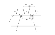
- a signal electrode S and a ground electrode G are formed on the substrate 1 as shown in a part of a cross section of the optical modulator in FIG.
- Reference numeral 2 denotes an optical waveguide formed on the substrate 1.
- the width of the signal electrode is gradually increased from the width (W1) of the portion closest to the substrate to the width (W2) of the portion farthest from the substrate.
- the interval between the signal electrode S and the ground electrode G is configured to gradually narrow from the interval (G1) closest to the substrate to the interval (G2) farthest from the substrate. .
- the modulation electrode having the shape as shown in FIG. 1 when the modulation electrode having the shape as shown in FIG. 1 is used, it is necessary to widen the gap G1 between the signal electrode and the ground electrode in order to widen the frequency response band. If it is increased, the drive voltage increases.
- Patent Document 1 also proposes a modulation electrode having a shape as shown in FIG.
- An electrode lower part (pedestal) 3 is formed on the substrate 1 and an electrode upper part is formed thereon, and the cross-sectional shape of the electrode is not continuous.
- the width (W2) of the upper part of the electrode is an electrode narrower than the width (W1) of the lower part of the electrode, and the distance (G1) between the signal electrode S and the ground electrode G in the lower part of the electrode is the distance (G2) of the upper part of the electrode. ) Is narrower than.
- a signal electrode and a ground electrode are formed.
- forming the electrode of FIG. 2 requires at least two electrode forming processes, which increases the time and cost required for electrode formation.
- the problem to be solved by the present invention is to provide an optical modulator capable of solving the above-described problems and capable of widening the frequency response characteristic while suppressing an increase in drive voltage, and further, manufacturing. It is an object to provide an optical modulator that suppresses an increase in time and cost.
- the invention according to claim 1 includes a substrate having an electro-optic effect, an optical waveguide formed on the substrate, and a modulation electrode for modulating a light wave propagating through the optical waveguide.
- the modulation electrode is a coplanar electrode composed of a signal electrode and a ground electrode arranged so as to sandwich the signal electrode, and a distance between the signal electrode and the ground electrode is determined from a portion closest to the substrate. It is configured to gradually widen in a direction away from the substrate, and at least the entire signal electrode is formed of a single material.
- the invention according to claim 2 is characterized in that, in the optical modulator according to claim 1, the distance between the signal electrode and the ground electrode is continuously changed.
- the invention according to claim 3 is the optical modulator according to claim 1 or 2, wherein the substrate is an X-cut substrate, and the thickness of the substrate is 20 ⁇ m or less.
- an optical modulator comprising a substrate having an electro-optic effect, an optical waveguide formed on the substrate, and a modulation electrode for modulating an optical wave propagating through the optical waveguide
- the modulation The electrode is a coplanar electrode composed of a signal electrode and a ground electrode arranged so as to sandwich the signal electrode, and the distance between the signal electrode and the ground electrode is in a direction away from the substrate from the portion closest to the substrate. Therefore, at least the entire signal electrode is made of a single material, so that an optical modulator capable of realizing a wide frequency response characteristic while suppressing an increase in driving voltage is provided. It becomes possible.
- the signal electrode can be formed by a single manufacturing process.
- the electrode manufacturing process becomes complicated as in the conventional optical modulator shown in FIG. And the increase in manufacturing time and manufacturing cost can be suppressed.
- the substrate is an X-cut substrate and the thickness of the substrate is 20 ⁇ m or less, the electric field formed by the modulation electrode can be efficiently applied to the optical waveguide, and the frequency response It becomes possible to further improve the characteristics.
- the present invention is an optical modulation having a substrate 1 having an electro-optic effect, an optical waveguide 2 formed on the substrate, and a modulation electrode for modulating an optical wave propagating through the optical waveguide.
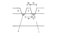
- the modulation electrode is a coplanar electrode composed of a signal electrode S and a ground electrode G disposed so as to sandwich the signal electrode S, and a distance (G1, G2) between the signal electrode and the ground electrode is determined by a substrate.
- the signal electrode (S) is configured to gradually widen from the portion closest to the substrate in a direction away from the substrate, and at least the entire signal electrode (S) is formed of a single material.
- any single crystal of LiNbO 3 , LiTaO 3 or PLZT (lead lanthanum zirconate titanate) can be suitably used.
- the optical waveguide formed on the substrate is formed, for example, by thermally diffusing a high refractive index material such as titanium (Ti) on a LiNbO 3 substrate (LN substrate).
- a rib-type optical waveguide in which grooves are formed on both sides of a portion that becomes an optical waveguide and a ridge-type waveguide in which the optical waveguide portion is convex can be used.
- the modulation electrode includes a signal electrode S and a ground electrode G, and can be formed by forming a Ti / Au electrode pattern on the surface of the substrate and using a gold plating method or the like. Furthermore, if necessary, a buffer layer such as dielectric SiO 2 can be provided on the substrate surface after the optical waveguide is formed. In the sense that “the entire signal electrode is composed of a single material” according to the present invention, as described above, in order to increase the bonding strength between the substrate and the material constituting the electrode, Providing a base such as an electrode pattern is not excluded.
- the distance between the signal electrode S and the ground electrode G constituting the modulation electrode is gradually increased from the portion closest to the substrate 1 toward the direction away from the substrate. Is to configure. Therefore, it is possible to form inclined side surfaces on both the signal electrode and the ground electrode as shown in FIG. 3, but as shown in FIG. Alternatively, as shown in FIG. 4B, it is also possible to provide an inclined side surface only on the ground electrode G.
- the modulation electrode can be formed by a single manufacturing process.
- reflection of the electric signal by the discontinuous portion and emission into the air are reduced, it is possible to suppress problems such as an increase in propagation loss and impedance mismatch due to reflection of the electric signal due to a sudden change in impedance.
- the “continuously changing” interval between the signal electrode and the ground electrode means that the interval changes smoothly in the height direction of the electrode.
- the impedance mismatch can be suppressed by smoothly changing the shape of the signal electrode along the propagation direction of the electric signal.
- the shape of the modulation electrode as in the present invention is basically such as a signal input pad portion along the signal electrode, and an action portion (a portion where the electric field formed by the modulation electrode acts on the optical waveguide) from the pad portion.
- an action portion a portion where the electric field formed by the modulation electrode acts on the optical waveguide
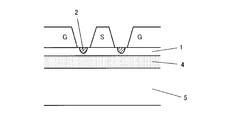
- FIG. 5 shows a configuration in which the thin substrate 1 is bonded to the reinforcing substrate 5 using an adhesive 4 or the like.
- the substrate used in the optical modulator of the present invention is an X-cut substrate, and the thickness of the substrate is more preferably 20 ⁇ m or less.
- the optical waveguide 2 is disposed between the signal electrode S and the ground electrode G, and therefore the distance between the signal electrode S and the ground electrode G closest to the substrate (G1) By narrowing, the electric field can be efficiently applied to the optical waveguide, and the drive voltage can be reduced.
- the confinement of the microwave that is the modulation signal is strengthened, an electric field can be efficiently applied to the optical waveguide, and speed matching between the microwave and the light wave can be achieved. It becomes possible.
- FIG. 6 shows a state in which pattern exposure is performed using the photomask 20 on the photoresist film 10 applied on the substrate 1.
- the light transmitted through the transmission part 21 of the photomask 20 exposes a predetermined pattern on the photoresist film 10.
- Reference numeral 22 denotes a non-transparent portion of the photomask
- reference numeral 11 denotes an exposed portion of the photoresist film
- reference numeral 12 denotes an unexposed portion of the photoresist film.
- a trapezoidal exposure pattern (11) can be formed by adjusting the temperature and time before and after the exposure, when the photoresist film is baked (cured). After this exposure, development is performed, the resist in the exposed portion 11 is removed, and a gold electrode can be formed on the portion 11 by plating.
- the exposure angle (trapezoidal exposure portion) as shown in FIG. 7 is obtained by changing the light irradiation angle as indicated by arrows a to c. 11) can be formed.
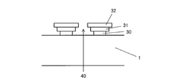
- resist patterns (30 to 32) having different shapes are stacked on the substrate 1 to form a space whose width gradually decreases from the substrate side to the top as indicated by reference numeral 40.
- the electrode material By filling this space with the electrode material, it is possible to form a signal electrode having a width (W2) narrower than the width (W1) on the substrate side.
- an optical modulator capable of widening the frequency response characteristic while suppressing an increase in driving voltage, and further, an increase in manufacturing time and cost. It is possible to provide an optical modulator that suppresses the above.
Landscapes
- Physics & Mathematics (AREA)
- Nonlinear Science (AREA)
- General Physics & Mathematics (AREA)
- Optics & Photonics (AREA)
- Chemical & Material Sciences (AREA)
- Engineering & Computer Science (AREA)
- Ceramic Engineering (AREA)
- Crystallography & Structural Chemistry (AREA)
- Optical Modulation, Optical Deflection, Nonlinear Optics, Optical Demodulation, Optical Logic Elements (AREA)
Abstract
駆動電圧の増加を抑制しながら周波数応答特性の広帯域化が可能な光変調器を提供することであり、さらには、製造に掛る時間やコストの増加を抑制した光変調器を提供することを目的とする。 電気光学効果を有する基板1と、該基板に形成された光導波路2と、該光導波路を伝搬する光波を変調するための変調電極とを有する光変調器において、該変調電極は、信号電極Sとそれを挟むように配置される接地電極Gとからなるコプレーナ型電極であり、該信号電極と該接地電極との間隔(G1,G2)は、基板に最も近い部分から基板からはなれる方向に向かって徐々に広くなるよう構成され、少なくとも該信号電極全体は、単一の材料から構成されることを特徴とする。
Description
本発明は、光変調器に関するものであり、特に、電気光学効果を有する基板に光導波路及び変調電極を形成した光変調器に関する。
光通信分野や光計測分野において、ニオブ酸リチウムなどの電気光学効果を有する基板に光導波路及び変調電極を形成した光変調器が多用されている。このような光変調器は、数十GHz以上の高速変調が可能であり、より一層の高速変調や周波数応答特性の改善が求められている。
光変調器の変調電極については、図1に光変調器の断面の一部を示すように、基板1上に信号電極S及び接地電極Gが形成されている。符号2は、基板1に形成された光導波路を示している。
図1のような形状の変調電極では、信号電極の幅が、基板に最も近い部分の幅(W1)から基板から最も離れた部分の幅(W2)へと徐々に幅が大きくなるように形成され、信号電極Sと接地電極Gとの間隔は、逆に、基板に最も近い部分の間隔(G1)から基板から最も離れた部分の間隔(G2)へと徐々に狭くなるよう構成されている。
しかしながら、図1のような形状の変調電極を利用する場合には、周波数応答帯域の広帯域化を図るためには、信号電極と接地電極との間隔G1を広くする必要があるが、間隔G1を大きくすると駆動電圧が上昇するという問題を生じる。
他方、特許文献1には、図2に示すような形状の変調電極も提案されている。基板1の上に電極下部(台座)3を形成し、その上に電極上部を形成し、電極の断面形状が連続的な形状とはなっていない。電極上部の幅(W2)は、電極下部の幅(W1)より幅の狭い電極であり、また、電極下部の信号電極Sと接地電極Gとの間隔(G1)は、電極上部の間隔(G2)よりも狭くなっている。信号電極や接地電極を形成している。
しかしながら、図2の電極を形成するには、少なくとも2回以上の電極形成プロセスが必要であり、電極形成に掛る時間やコストが増大する原因となる。
本発明が解決しようとする課題は、上述したような問題を解決し、駆動電圧の増加を抑制しながら周波数応答特性の広帯域化が可能な光変調器を提供することであり、さらには、製造に掛る時間やコストの増加を抑制した光変調器を提供することである。
上記課題を解決するため、請求項1に係る発明は、電気光学効果を有する基板と、該基板に形成された光導波路と、該光導波路を伝搬する光波を変調するための変調電極とを有する光変調器において、該変調電極は、信号電極とそれを挟むように配置される接地電極とからなるコプレーナ型電極であり、該信号電極と該接地電極との間隔は、基板に最も近い部分から基板からはなれる方向に向かって徐々に広くなるよう構成され、少なくとも該信号電極全体は、単一の材料から構成されることを特徴とする。
請求項2に係る発明は、請求項1に記載の光変調器において、該信号電極と該接地電極との間隔は連続的に変化するよう構成されていることを特徴とする。
請求項3に係る発明は、請求項1又は2に記載の光変調器において、該基板はXカット型の基板であり、該基板の厚みは、20μm以下であることを特徴とする。
請求項1に係る発明により、電気光学効果を有する基板と、該基板に形成された光導波路と、該光導波路を伝搬する光波を変調するための変調電極とを有する光変調器において、該変調電極は、信号電極とそれを挟むように配置される接地電極とからなるコプレーナ型電極であり、該信号電極と該接地電極との間隔は、基板に最も近い部分から基板からはなれる方向に向かって徐々に広くなるよう構成され、少なくとも該信号電極全体は、単一の材料から構成されるため、駆動電圧の増加を抑制しながら周波数応答特性の広帯域化を実現可能な光変調器を提供することが可能となる。しかも、少なくとも信号電極全体が単一の材料で構成されるため、1度の製造プロセスで信号電極を形成することも可能となる。
請求項2に係る発明により、信号電極と接地電極との間隔は連続的に変化するよう構成されているため、図2に示した従来の光変調器のように、電極の製造工程が複雑化することが抑制され、製造時間や製造コストの増加も抑えられる。
請求項3に係る発明により、基板はXカット型の基板であり、基板の厚みは、20μm以下であるため、変調電極が形成する電界を効率良く光導波路に印加することが可能となり、周波数応答特性をより改善することも可能となる。
以下、本発明の光変調器について、好適例を用いて詳細に説明する。
図3に示すように、本発明は、電気光学効果を有する基板1と、該基板に形成された光導波路2と、該光導波路を伝搬する光波を変調するための変調電極とを有する光変調器において、該変調電極は、信号電極Sとそれを挟むように配置される接地電極Gとからなるコプレーナ型電極であり、該信号電極と該接地電極との間隔(G1,G2)は、基板に最も近い部分から基板からはなれる方向に向かって徐々に広くなるよう構成され、少なくとも該信号電極(S)全体は、単一の材料から構成されることを特徴とする。
図3に示すように、本発明は、電気光学効果を有する基板1と、該基板に形成された光導波路2と、該光導波路を伝搬する光波を変調するための変調電極とを有する光変調器において、該変調電極は、信号電極Sとそれを挟むように配置される接地電極Gとからなるコプレーナ型電極であり、該信号電極と該接地電極との間隔(G1,G2)は、基板に最も近い部分から基板からはなれる方向に向かって徐々に広くなるよう構成され、少なくとも該信号電極(S)全体は、単一の材料から構成されることを特徴とする。
電気光学効果を有する基板1としては、特に、LiNbO3,LiTaO3又はPLZT(ジルコン酸チタン酸鉛ランタン)のいずれかの単結晶が好適に利用可能である。また、基板に形成する光導波路は、例えば、LiNbO3基板(LN基板)上にチタン(Ti)などの高屈折率物質を熱拡散することにより形成される。また、光導波路となる部分の両側に溝を形成したリブ型光導波路や光導波路部分を凸状としたリッジ型導波路も利用可能である。
変調電極は、信号電極Sや接地電極Gから構成され、基板表面に、Ti・Auの電極パターンを形成し、金メッキ方法などにより形成することが可能である。さらに、必要に応じて光導波路形成後の基板表面に誘電体SiO2等のバッファ層を設けることも可能である。なお、本発明に係る「信号電極全体は、単一の材料で構成される」との意味において、上述のように、基板と電極を構成する材料との接合強度を高めるため、Ti・Auの電極パターンのような下地を設けることは、排除していない。
本発明の光変調器の特徴の一つは、変調電極を構成する信号電極Sと接地電極Gとの間隔を、基板1に最も近い部分から基板からはなれる方向に向かって徐々に広くなるよう構成することである。このため、図3に示すように信号電極と接地電極の両方に傾斜した側面を形成することも可能であるが、図4(a)に示すように、信号電極Sのみに傾斜した側面を設けたり、図4(b)に示すように、接地電極Gのみに傾斜した側面を設けることも可能である。
少なくとも信号電極全体を単一の材料で構成することで、電極の製造工程が複雑化することが抑制される。しかも、信号電極の部分毎に異なる材料を使用する場合には、電気信号の伝搬にムラが発生し易くなり、信号の伝搬損失が増加したり、光導波路へ印加される電界にムラ、更にはインピーダンスの急激な変化による電気信号の反射によるインピーダンス不整合が生じるなどの不具合も発生する。
また、信号電極と接地電極との間隔は連続的に変化するよう構成することで、1度の製造プロセスで変調電極を形成することも可能となる。また、不連続部分よる電気信号の反射や空気中への放出が減少するため、伝搬損失の増大、インピーダンスの急激な変化による電気信号の反射によるインピーダンス不整合などの不具合が抑制できる。
ここで、信号電極と接地電極との間隔が「連続的に変化する」とは、電極の高さ方向に向かって該間隔が滑らかに変化することを意味している。なお、信号電極の電気信号の伝播方向に沿って形状が滑らかに変化することで、インピーダンス不整合を抑制できる。
また、本発明のような変調電極の形状は、信号電極に沿って、信号入力用パッド部、該パッド部から作用部(変調電極が形成する電界が光導波路に作用する部分)など、基本的には、信号電極の全てに渡って適用することが好ましいが、少なくとも作用部に適用するだけでも十分に周波数応答特性を改善することが可能となる。
図5は、薄板の基板1を、接着剤4などを用いて補強基板5に接合した構成を示している。図5に示すように、本発明の光変調器に使用される基板は、Xカット型の基板であり、基板の厚みは、20μm以下であることがより好ましい。Xカット型基板を用いた場合には、信号電極Sと接地電極Gとの間に光導波路2が配置されるため、信号電極Sと接地電極Gとの基板に最も近い部分の間隔(G1)を狭くすることで、電界を効率良く光導波路に印加でき、駆動電圧の低減を図ることが可能である。
また、20μm以下の厚みを有する薄板を利用することで、変調信号であるマイクロ波の閉じ込めが強くなり、光導波路に効率良く電界を印加できると共に、マイクロ波と光波との速度整合も図ることが可能となる。
図6乃至8は、電極の製造プロセスの一部を示す図である。
図6では、基板1上に塗布したフォトレジスト膜10にフォトマスク20を用いて、パターン露光を行う様子を示している。フォトマスク20の透過部21を透過した光は、フォトレジスト膜10に所定のパターンを露光する。符号22はフォトマスクの不透過部であり、符号11はフォトレジスト膜の露光部分、符号12は、フォトレジスト膜の非露光部分を各々示している。
図6では、基板1上に塗布したフォトレジスト膜10にフォトマスク20を用いて、パターン露光を行う様子を示している。フォトマスク20の透過部21を透過した光は、フォトレジスト膜10に所定のパターンを露光する。符号22はフォトマスクの不透過部であり、符号11はフォトレジスト膜の露光部分、符号12は、フォトレジスト膜の非露光部分を各々示している。
図6では、露光の前後において、フォトレジスト膜のベーク時(硬化時)に、温度や時間を調整することで、台形の露光パターン(11)を形成することが可能である。この露光終了後、現像を行い、露光部11のレジストを除去し、メッキにより金の電極を符号11の部分に形成することが可能である。
図7では、フォトマスク20を用いてフォトレジスト膜10を露光する際に、矢印a~cのように、光の照射角度を変化させることで、図7のような露光パターン(台形の露光部11)を形成することが可能となる。
図8では、基板1の上に、形状の異なるレジストパターン(30~32)を積み上げることで、符号40で示すような基板側から上に向かって徐々に幅が狭くなる空間を形成する。この空間に電極材料を充填することで、基板側の幅(W1)より上側の幅(W2)が狭い信号電極を形成することが可能となる。
本発明に係る光変調器として、図3の形状において、W1=30μm、W2=26μm、G1=20μm、G2=24μmとした場合の周波数応答特性をシュミレーションした結果を図9に示す。また、従来例として、図1の形状において、W1=30μm、W2=34μm、G1=20μm、G2=16μmとした場合についても同様に、図9に示す。
図9の結果から、本発明の光変調器の方が、周波数応答特性が格段に改善していることが容易に理解される。
以上説明したように、本発明によれば、駆動電圧の増加を抑制しながら周波数応答特性の広帯域化が可能な光変調器を提供することであり、さらには、製造に掛る時間やコストの増加を抑制した光変調器を提供することが可能となる。
1 基板
2 光導波路
3 電極下部
4 接着剤
5 補強基板
10 フォトレジスト膜
20 フォトマスク
2 光導波路
3 電極下部
4 接着剤
5 補強基板
10 フォトレジスト膜
20 フォトマスク
Claims (3)
- 電気光学効果を有する基板と、該基板に形成された光導波路と、該光導波路を伝搬する光波を変調するための変調電極とを有する光変調器において、
該変調電極は、信号電極とそれを挟むように配置される接地電極とからなるコプレーナ型電極であり、
該信号電極と該接地電極との間隔は、基板に最も近い部分から基板からはなれる方向に向かって徐々に広くなるよう構成され、
少なくとも該信号電極全体は、単一の材料から構成されることを特徴とする光変調器。 - 請求項1に記載の光変調器において、該信号電極と該接地電極との間隔は連続的に変化するよう構成されていることを特徴とする光変調器。
- 請求項1又は2に記載の光変調器において、該基板はXカット型の基板であり、該基板の厚みは、20μm以下であることを特徴とする光変調器。
Applications Claiming Priority (2)
| Application Number | Priority Date | Filing Date | Title |
|---|---|---|---|
| JP2010-082232 | 2010-03-31 | ||
| JP2010082232A JP2011215294A (ja) | 2010-03-31 | 2010-03-31 | 光変調器 |
Publications (1)
| Publication Number | Publication Date |
|---|---|
| WO2011125692A1 true WO2011125692A1 (ja) | 2011-10-13 |
Family
ID=44762636
Family Applications (1)
| Application Number | Title | Priority Date | Filing Date |
|---|---|---|---|
| PCT/JP2011/057939 Ceased WO2011125692A1 (ja) | 2010-03-31 | 2011-03-30 | 光変調器 |
Country Status (2)
| Country | Link |
|---|---|
| JP (1) | JP2011215294A (ja) |
| WO (1) | WO2011125692A1 (ja) |
Cited By (1)
| Publication number | Priority date | Publication date | Assignee | Title |
|---|---|---|---|---|
| CN116266018A (zh) * | 2022-07-17 | 2023-06-20 | 上海图灵智算量子科技有限公司 | 电光调制器及光计算网络 |
Families Citing this family (1)
| Publication number | Priority date | Publication date | Assignee | Title |
|---|---|---|---|---|
| JPWO2024069952A1 (ja) * | 2022-09-30 | 2024-04-04 |
Citations (1)
| Publication number | Priority date | Publication date | Assignee | Title |
|---|---|---|---|---|
| JP2009086336A (ja) * | 2007-09-28 | 2009-04-23 | Sumitomo Osaka Cement Co Ltd | 光導波路型デバイス |
-
2010
- 2010-03-31 JP JP2010082232A patent/JP2011215294A/ja active Pending
-
2011
- 2011-03-30 WO PCT/JP2011/057939 patent/WO2011125692A1/ja not_active Ceased
Patent Citations (1)
| Publication number | Priority date | Publication date | Assignee | Title |
|---|---|---|---|---|
| JP2009086336A (ja) * | 2007-09-28 | 2009-04-23 | Sumitomo Osaka Cement Co Ltd | 光導波路型デバイス |
Non-Patent Citations (1)
| Title |
|---|
| M. GOANO ET AL.: "A general conformal-mapping approach to the optimum electrode design of coplanar waveguide with arbitrary cross section", IEEE TRANSACTIONS ON MICROWAVE THEORY AND TECHNIQUES, vol. 49, no. 9, September 2001 (2001-09-01), pages 1573 - 1577, XP001096608, DOI: doi:10.1109/22.942569 * |
Cited By (1)
| Publication number | Priority date | Publication date | Assignee | Title |
|---|---|---|---|---|
| CN116266018A (zh) * | 2022-07-17 | 2023-06-20 | 上海图灵智算量子科技有限公司 | 电光调制器及光计算网络 |
Also Published As
| Publication number | Publication date |
|---|---|
| JP2011215294A (ja) | 2011-10-27 |
Similar Documents
| Publication | Publication Date | Title |
|---|---|---|
| JP5298849B2 (ja) | 光制御素子 | |
| JP4445977B2 (ja) | 光制御素子 | |
| JP4110182B2 (ja) | 光制御素子 | |
| US8923658B2 (en) | Optical waveguide device | |
| CN101416098B (zh) | 光调制器 | |
| CN216411633U (zh) | 光波导元件及使用光波导元件的光调制器件和光发送装置 | |
| US10185165B2 (en) | Optical waveguide device | |
| JP4187771B2 (ja) | 光制御素子 | |
| US8391651B2 (en) | Optical waveguide device | |
| JP2008250258A (ja) | 光制御素子 | |
| JP2009244812A (ja) | 光導波路素子 | |
| JP7259486B2 (ja) | 光変調器 | |
| JP2010072129A (ja) | 電子デバイス | |
| JP4958771B2 (ja) | 光制御素子 | |
| JP2013037243A (ja) | 光変調器 | |
| WO2007020924A1 (ja) | 光変調器 | |
| WO2011125692A1 (ja) | 光変調器 | |
| JP2010085789A (ja) | 光導波路素子 | |
| JP6398382B2 (ja) | 光デバイス | |
| JP7207086B2 (ja) | 光変調器 | |
| JP7052477B2 (ja) | 光導波路素子 | |
| WO2025069334A1 (ja) | 光導波路素子及びそれを用いた光変調器並びに光送信装置 | |
| JP2020060742A (ja) | 光導波路素子および光変調器 | |
| WO2004086126A1 (ja) | 導波路型光変調器 | |
| JP4354464B2 (ja) | 光導波路素子 |
Legal Events
| Date | Code | Title | Description |
|---|---|---|---|
| 121 | Ep: the epo has been informed by wipo that ep was designated in this application |
Ref document number: 11765592 Country of ref document: EP Kind code of ref document: A1 |
|
| NENP | Non-entry into the national phase |
Ref country code: DE |
|
| 122 | Ep: pct application non-entry in european phase |
Ref document number: 11765592 Country of ref document: EP Kind code of ref document: A1 |