WO2011122162A1 - Antenne composite, et dispositif de radiocommunications composite - Google Patents
Antenne composite, et dispositif de radiocommunications composite Download PDFInfo
- Publication number
- WO2011122162A1 WO2011122162A1 PCT/JP2011/053655 JP2011053655W WO2011122162A1 WO 2011122162 A1 WO2011122162 A1 WO 2011122162A1 JP 2011053655 W JP2011053655 W JP 2011053655W WO 2011122162 A1 WO2011122162 A1 WO 2011122162A1
- Authority
- WO
- WIPO (PCT)
- Prior art keywords
- antenna
- composite
- frequency band
- wireless communication
- main surface
- Prior art date
Links
Images


Classifications
-
- H—ELECTRICITY
- H01—ELECTRIC ELEMENTS
- H01Q—ANTENNAS, i.e. RADIO AERIALS
- H01Q7/00—Loop antennas with a substantially uniform current distribution around the loop and having a directional radiation pattern in a plane perpendicular to the plane of the loop
-
- H—ELECTRICITY
- H01—ELECTRIC ELEMENTS
- H01Q—ANTENNAS, i.e. RADIO AERIALS
- H01Q1/00—Details of, or arrangements associated with, antennas
- H01Q1/12—Supports; Mounting means
- H01Q1/22—Supports; Mounting means by structural association with other equipment or articles
- H01Q1/2208—Supports; Mounting means by structural association with other equipment or articles associated with components used in interrogation type services, i.e. in systems for information exchange between an interrogator/reader and a tag/transponder, e.g. in Radio Frequency Identification [RFID] systems
-
- H—ELECTRICITY
- H01—ELECTRIC ELEMENTS
- H01Q—ANTENNAS, i.e. RADIO AERIALS
- H01Q1/00—Details of, or arrangements associated with, antennas
- H01Q1/36—Structural form of radiating elements, e.g. cone, spiral, umbrella; Particular materials used therewith
- H01Q1/38—Structural form of radiating elements, e.g. cone, spiral, umbrella; Particular materials used therewith formed by a conductive layer on an insulating support
-
- H—ELECTRICITY
- H01—ELECTRIC ELEMENTS
- H01Q—ANTENNAS, i.e. RADIO AERIALS
- H01Q21/00—Antenna arrays or systems
- H01Q21/30—Combinations of separate antenna units operating in different wavebands and connected to a common feeder system
Definitions
- the present invention relates to a composite antenna and a composite wireless communication device, and more particularly to a composite antenna that resonates in two different frequency bands and a composite wireless communication device including the composite antenna.
- Patent Document 1 discloses a wireless card having a wire antenna in which a wire is wound in a coil shape and a pattern antenna formed smaller than the inner diameter of the wire antenna. Are listed. However, in this wireless card, the wire antenna and the pattern antenna are not associated with each other, and processing such as using one antenna for improving the gain of the other antenna is not considered.
- the two different frequency bands used as the antenna are, for example, one 13.56 MHz band used in an RFID (Radio Frequency Identification) system, and the other used as a crime detection target (also called a crime prevention tag).
- the band is 8.2 MHz.
- the security tag includes an antenna that can communicate at a relatively long distance using an electromagnetic field. Since an antenna used in a wireless communication device for RFID uses a magnetic field, communication is performed at a relatively short distance. Although it is preferable if the RFID antenna can function as a security tag, it is difficult because the communication distance is short at present. Therefore, at present, it is necessary to separately provide a wireless communication device for managing articles and a dedicated tag for crime prevention.
- an object of the present invention is to improve the gain of the second antenna by correlating two antennas that resonate in different frequency bands, and to use it as a single antenna even in the first frequency band. And providing a composite wireless communication device.
- a composite antenna includes an insulating substrate having a first main surface and a second main surface, a first antenna that resonates in a first frequency band, A second antenna that resonates in a second frequency band higher than the first frequency band, and the first antenna is formed in a state of facing the first main surface and the second main surface of the insulating substrate. It is comprised by a coil-shaped electrode, The 1st antenna and the 2nd antenna are electrically connected by the 1st or 2nd main surface of the said insulating base material, It is characterized by the above-mentioned.
- a composite wireless communication device includes the composite antenna and a wireless communication element that processes a high-frequency signal, and the wireless communication element is coupled to the second antenna. To do.
- the first antenna functions as an electromagnetic field antenna that resonates in a first frequency band (for example, 8.2 MHz band).
- the second antenna resonates in a second frequency band (for example, 13.56 MHz band) higher than the first frequency band, and functions as a magnetic field antenna.
- the first antenna is electrically connected to the second antenna on one surface of the insulating base material, and thus becomes a capacitive component and functions as a radiating element.
- the first antenna functions as a radiating element (boost antenna) of the second antenna, and the gain is improved.
- the second antenna is configured as a wireless communication device (wireless IC tag) that communicates with the reader / writer of the RFID system by coupling a wireless communication element. If the wireless communication element is omitted, it can be configured as a security tag using only the first antenna. That is, in the composite antenna, communication in the first frequency band and the second frequency band is possible by providing a wireless communication element, and communication in only the first frequency band is possible by omitting the wireless communication element. Is possible.
- two antennas that resonate in different frequency bands can be associated with each other to improve the gain of the second antenna, and can be used as a single antenna only in the first frequency band. is there.
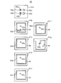
- the composite antenna which is 1st Example is shown, (A) is a front view, (B) is a back surface perspective view. It is a perspective view which shows the electric power feeding circuit board carrying a radio
- the composite antenna which is 2nd Example is shown, (A) is a front view, (B) is a back surface perspective view.
- the composite antenna which is 3rd Example is shown, (A) is a front view, (B) is a back surface perspective view.
- the composite antenna which is 4th Example is shown, (A) is a front view, (B) is a back surface perspective view.
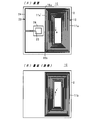
- the composite antenna 1A has an insulating substrate 2, a first antenna 10 that resonates in the first frequency band, and a second frequency band higher than the first frequency band. And a second antenna 20 that resonates.
- the insulating substrate 2 is made of, for example, paper or PET film.
- the first antenna 10 and the second antenna 20 have the same external shape.
- the first antenna 10 includes first and second coiled electrodes 11a and 11b that are formed on the first main surface (front surface) and the second main surface (back surface) of the insulating substrate 2 so as to face each other.
- the first and second coiled electrodes 11a and 11b have a coiled pattern on the front and back surfaces of the substrate 2 in the opposite directions from the center (the first coiled electrode 11a on the front surface is in the direction of arrow a and the second coiled surface on the back surface.
- the coiled electrode 11b is wound (in the direction of arrow a ′) and is capacitively coupled via the insulating substrate 2. Thereby, the direction of the electric current which flows into the 1st and 2nd coiled electrodes 11a and 11b becomes the same, and the magnetic field (synthetic magnetic field) which arises in each coiled electrode 11a and 11b can be strengthened.
- the second antenna 20 includes first and second coiled electrodes 21a and 21b formed on the front and back surfaces of the insulating base 2 so as to face each other, and is spirally wound around the center. 1 and 2nd coupling
- the first and second coiled electrodes 21a and 21b have a coiled pattern on the front and back surfaces of the base material 2 in opposite directions from the center (the first coiled electrode 21a on the front surface is in the direction of arrow b and the second coiled surface on the back surface).
- the coiled electrode 21 b is wound in the direction of the arrow b ′ and is capacitively coupled via the insulating base material 2.
- the winding directions of the first and second coupling portions 22 a and 22 b are also opposite to each other (see arrows c and c ′), and are capacitively coupled via the insulating substrate 2.
- the directions of the currents flowing through the first and second coiled electrodes 21a and 21b are the same, and the magnetic field (synthetic magnetic field) generated in each of the coiled electrodes 21a and 21b is strengthened. Can do.
- the first antenna 10 and the second antenna 20 are electrically connected on the surface of the base material 2.
- the connecting portion 15 is one place where the first coiled electrode 11a of the first antenna 10 and the first coiled electrode 21a of the second antenna 20 are adjacent to each other at the outer periphery.
- the first antenna 10 and the second antenna 20 are not electrically (DC) connected on the back surface of the substrate.
- a wireless communication element 30 shown in FIG. 2 is disposed on the first coupling portion 22a of the second antenna 20.
- the wireless communication element 30 includes a wireless IC chip 31 that processes a high-frequency signal and a power supply circuit board 35 having a power supply circuit.
- the wireless IC chip 31 includes a clock circuit, a logic circuit, a memory circuit, and the like, and necessary information is stored therein.
- An input terminal electrode, an output terminal electrode, and a mounting terminal (not shown) An electrode is provided.
- the power supply circuit board 35 is a laminated board including a power supply circuit including an inductor, and is mounted (adhered) on the first coupling portion 22 a.
- the wireless communication element 30 is one in which the wireless IC chip 31 and the power feeding circuit board 35 are separately formed, and the wireless IC and the power feeding circuit are integrally formed on one board. Also good.
- the wireless IC chip 31 is made to function as a single wireless communication element.
- the power supply circuit board 35 is formed by laminating a plurality of sheets 41a to 41g each having an electrode, and each of the sheets 41a to 41g is made of ceramic or resin.
- electrodes 42a to 42d and via-hole conductors 43a and 43b are formed.
- electrodes 44 and via-hole conductors 43c and 43d are formed.
- An electrode 44 is formed on the sheet 41g.
- the respective electrodes 44 are electrically connected via the via-hole conductors 43d to form inductors.
- One end of the inductor (one end 44a of the electrode 44 on the sheet 41b) is connected to the electrode 42b on the sheet 41a via the via-hole conductor 43b.
- the other end of the inductor (one end 44b of the electrode 44 on the sheet 41g) is connected to the electrode 42a on the sheet 41a via the via-hole conductors 43c and 43a.
- the inductor resonates at a predetermined resonance frequency with its own inductance and the capacitance between the electrodes 44.
- the electrodes 42a and 42b on the sheet 41a are connected to the input terminal electrode and the output terminal electrode of the wireless IC chip 31, respectively.
- the electrodes 42c and 42d on the sheet 41a are connected to the mounting terminal electrodes of the wireless IC chip 31.
- the inductor is magnetically coupled to the first and second coupling portions 22a and 22b.
- the first antenna 10 forms a resonance circuit with the inductance formed by the first and second coiled electrodes 11a and 11b and the capacitance formed by the electrodes 11a and 11b facing each other. It functions as an electromagnetic field antenna that resonates in a predetermined first frequency band (for example, 8.2 MHz band). Therefore, the high frequency of the 1st frequency band radiated
- a predetermined first frequency band for example, 8.2 MHz band
- the first antenna 10 can increase the inductance value, that is, the impedance, and expand the communication area by increasing the number of turns of the coiled electrodes 11a and 11b. And when the overlapping part of coiled electrode 11a, 11b increases, the capacitance between coiled electrode 11a, 11b will also become large, and articles
- the second antenna 20 forms a resonance circuit by the inductance formed by the first and second coiled electrodes 21a and 21b and the capacitance formed by the electrodes 21a and 21b facing each other, and the first frequency band. Resonance in a higher second frequency band (for example, 13.56 MHz band), and functions as a magnetic field antenna.
- the first and second coupling portions 22 a and 22 b are magnetically coupled to the power supply circuit board 35 constituting the wireless communication element 30.
- the high frequency signal for example, UHF frequency band and HF frequency band
- the high frequency signal for example, UHF frequency band and HF frequency band
- the power feeding circuit that is magnetically coupled to the first and second coupling portions 22 a and 22 b is resonated, and only a reception signal having a predetermined frequency is supplied to the wireless IC chip 31.
- the wireless IC chip 31 takes out predetermined energy from the received signal, reads out information stored using this energy as a drive source, matches it with a predetermined frequency in the power feeding circuit, and then the first and second coupling units 22a, It radiates
- the first antenna 10 is electrically connected to the second antenna 20 through the connection portion 15, and therefore a current in the second frequency band flows through the first antenna 10.
- the magnetic fluxes in the direction of the winding axis 20 are strengthened each other.
- the first antenna 10 that resonates in the first frequency band lower than the second frequency band does not resonate with the current in the second frequency band, and becomes a distributed constant type capacitance component, the current of the first antenna 10 Flows so as to form a magnetic field in the same direction as the second antenna 20.
- the radiation area of the magnetic field is expanded, and the first antenna 10 functions as a boost antenna when the second antenna 20 is operated.
- the gain in the second frequency band is improved.
- the communication distance at 13.56 MHz is 1.5 times that when the second antenna 20 is operated alone. More than that.
- the composite antenna 1A is configured as a wireless communication device (wireless IC tag) that communicates with the reader / writer of the RFID system by coupling the wireless communication element 30 to the second antenna 20. If the wireless communication element 30 is omitted, it can be configured as a security tag using only the first antenna 10. In other words, the wireless communication element 30 can be retrofitted, and a function as an RFID tag can be added as needed only by preparing the composite antenna 1A.
- wireless communication device wireless IC tag
- the second antenna 20 is an open type, and the coupling portions 22a and 22b also form an LC resonator. That is, a capacitance is formed between the coupling portions 22a and 22b arranged opposite to each other, and LC resonance is caused by the inductance formed by this capacitance and the spiral coupling portions 22a and 22b. Due to this LC resonance, the impedance becomes infinite, and energy is concentrated in the coupling portions 22a and 22b. As a result, energy transmission efficiency between the second antenna 20 and the wireless IC chip 31 mounted thereon is improved.
- the two coupling portions 22a and 22b facing each other are wound in opposite directions from the center portion in plan view, so that the current flows in the same direction and the directions of the magnetic fields coincide with each other. Will improve.
- the resonance frequency of the power feeding circuit substantially corresponds to the resonance frequency of the transmission / reception signal. That is, the resonance frequency of the wireless communication device is determined by the resonance frequency of the resonance circuit. Therefore, communication at the resonance frequency of the resonance circuit is possible regardless of the resonance frequency of the second antenna 20, and the power supply circuit board 35 having various resonance frequencies can be combined with one type of the second antenna 20. In addition, since the resonance frequency of the resonance circuit does not change due to the influence from others, the communication with the reader / writer is stable.
- the resonance frequency of the second antenna 20 is set higher than the resonance frequency of the resonance circuit included in the feeder circuit board 35.
- the resonance frequency of the second antenna 20 is set to 14 MHz.
- the power feeding circuit and the second antenna 20 are always magnetically coupled. If the second antenna 20 alone is viewed, the communication distance becomes longer when the resonance frequency is close to the resonance frequency of the resonance circuit.
- the resonance frequency of the second antenna 20 is preferably set on the high frequency side.
- first and second coupling portions 22a and 22b are disposed immediately below the magnetic field radiated from the power feeding circuit board 35, and the inductor in the power feeding circuit board 35 flows in the same direction as the coupling portions 22a and 22b. When formed in a spiral shape, energy can be transmitted more efficiently.
- the wireless IC chip 31 and the power supply circuit board 35 are electrically connected via a DC connection or an electromagnetic field. Further, the feeder circuit board 35 and the second antenna 20 are coupled via an electromagnetic field. Therefore, it is only necessary to join with an insulating adhesive.
- the direction of joining is also arbitrary, and since the area of the coupling parts 22a and 22b is larger than the area of the power feeding circuit board 35, alignment when the power feeding circuit board 35 is mounted on the coupling part 22a is extremely easy.
- the material of the insulating substrate 2 will be described.
- the thickness of the paper is preferably 50 ⁇ m or more in terms of strength. Since paper has higher heat resistance than organic materials such as PET film, it can withstand when it is attached to an article to be thermally sterilized. In addition, since printing does not generate waste liquid when the antennas 10 and 20 are formed by etching, environmental pollution does not occur. Furthermore, if the composite antenna is formed of paper and a conductive paste, the paste and paper can be easily separated using a solution during recycling and can be easily reused.
- the composite antenna 1B according to the second embodiment resonates in the insulating base 2, the first antenna 10 that resonates in the first frequency band, and the second frequency band that is higher than the first frequency band.
- the second antenna 20 is provided.
- the first antenna 10 is composed of first and second coiled electrodes 11a and 11b that are formed on the first main surface (front surface) and the second main surface (back surface) of the antistatic substrate 2 so as to face each other. It is configured.
- the first and second coiled electrodes 11a and 11b have a coiled pattern on the front and back surfaces of the substrate 2 in the opposite directions from the center (the first coiled electrode 11a on the front surface is in the direction of arrow a and the second coiled surface on the back surface.
- the coiled electrode 11b is wound in the direction of arrow a ′. Thereby, the direction of the electric current which flows into the 1st and 2nd coiled electrodes 11a and 11b becomes the same, and an electromagnetic field can be strengthened.
- the second antenna 20 is configured as a loop electrode 23 using a part of the first coiled electrode 11 a (one side 11 a ′ on the outer peripheral portion) on the surface of the insulating base 2. Both ends of the loop electrode 23 are electrically connected at two locations on the outer peripheral portion of the first coil electrode 11a (connection portions 15a and 15b), and the end portions are coupling portions (first and second) with the wireless IC chip 31. Second coupling portions 24a and 24b).
- the second antenna 20 is electrically connected to the input / output terminal electrodes of the wireless IC chip 31 directly at the coupling portions 24a and 24b.
- the power feeding circuit board 35 on which the wireless IC chip 31 is mounted may be coupled to the coupling portions 24a and 24b.
- the coupling portions 24a and 24b may be coupled to the feeder circuit board 35 as the spiral coupling portions 22a and 22b described in the first embodiment.
- the operations of the first antenna 10 and the second antenna 20 are basically the same as those of the composite antenna 1A.
- the first antenna 10 forms a resonant circuit with the inductances of the first and second coiled electrodes 11a and 11b and the capacitance formed by the electrodes 11a and 11b facing each other. It functions as an electromagnetic field antenna that resonates in the first frequency band (for example, 8.2 MHz band).
- the second antenna 20 mainly forms a resonance circuit with the inductance of the loop electrode 23, and is a second frequency band higher than the first frequency band (for example, a frequency band higher than the first frequency band such as the UHF band). It functions as a magnetic field antenna.
- the first antenna 10 is electrically connected to the second antenna 20 through the connection portions 15 a and 15 b, and therefore a current in the second frequency band flows through the first antenna 10.
- the first antenna 10 that resonates in the first frequency band lower than the second frequency band does not resonate with the current in the second frequency band.
- the first antenna 10 appears as a metal plate at the operating frequency of the second antenna, and functions as a boost antenna.
- the loop electrode 23 has a function of adjusting impedance with respect to the wireless IC chip 31. When the power supply circuit board 35 is used, the loop electrode 23 functions as a connection line.
- the first antenna 10 communicates with the security system
- the second antenna 20 communicates with the RFID system
- the first antenna 10 has a boost function when the second antenna 20 operates
- the wireless communication element 30 As described in the first embodiment, the security system or the RFID system can be used independently depending on the presence or absence.
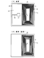
- the composite antenna 1C according to the third embodiment resonates in the insulating base 2, the first antenna 10 that resonates in the first frequency band, and the second frequency band that is higher than the first frequency band.
- the second antenna 20 is provided.
- the first antenna 10 is composed of first and second coiled electrodes 11a and 11b that are formed on the first main surface (front surface) and the second main surface (back surface) of the antistatic substrate 2 so as to face each other. It is configured.
- the first and second coiled electrodes 11a and 11b have a coiled pattern on the front and back surfaces of the substrate 2 in the opposite directions from the center (the first coiled electrode 11a on the front surface is in the direction of arrow a and the second coiled surface on the back surface.
- the coiled electrode 11b is wound in the direction of arrow a ′.
- the second antenna 20 is configured on the surface of the insulating substrate 2 as a loop electrode 24 using a part of the first coiled electrode 11a (one side 11a 'of the outer peripheral portion). Both ends of the loop electrode 24 are electrically connected at two locations on the outer periphery of the first coiled electrode 11a (connection portions 15a and 15b), and the end portion is a loop-shaped coupling portion 26 having a slit portion 25. Yes.
- the second antenna 20 resonates in a second frequency band (for example, 13.56 MHz band) higher than the first frequency band, and functions as a magnetic field antenna.
- the operations of the first antenna 10 and the second antenna 20 are the same as those of the composite antenna 1A.
- the first antenna 10 forms a resonant circuit with the inductances of the first and second coiled electrodes 11a and 11b and the capacitance formed by the electrodes 11a and 11b facing each other. It functions as an electromagnetic field antenna that resonates in the first frequency band (for example, 8.2 MHz band).
- the second antenna 20 resonates in a second frequency band (for example, 13.56 MHz band) higher than the first frequency band, and functions as a magnetic field antenna.
- the first antenna 10 serves as a capacitive component and functions as a boost antenna, as in the first embodiment.
- the second antenna 20 is coupled to the feeder circuit board 35 on which the wireless IC chip 31 is mounted by the loop coupling portion 26.
- the second antenna 20 has a relatively large loop-shaped electrode 24, and the communication distance with the reader / writer of the RFID system can be increased by rotating the magnetic field greatly.
- the composite antenna 1D according to the fourth embodiment is a solid electrode 24 ′ in which the inner part of the loop electrode 24 is filled with a conductive material in the composite antenna 1C according to the third embodiment.
- a slit 25 and an opening 27 are formed in the solid electrode 24 ′.
- the periphery of the opening 27 serves as a coupling portion with the feeder circuit board 35.
- a high-frequency current flows through the outer peripheral portion of the solid electrode 24 ′ and the edge portion of the slit portion 25, and functions as the second antenna 20.
- the operational effects of the fourth embodiment are the same as those of the third embodiment.
- the second antenna 20 can be formed with a simple configuration.
- composite antenna and the composite wireless communication device according to the present invention are not limited to the above-described embodiments, and can be variously modified within the scope of the gist thereof.
- the present invention is useful for a composite antenna and a composite wireless communication device, and is particularly advantageous in that the gain of the second antenna is improved and the antenna can be used as a single antenna only in the first frequency band. ing.
Abstract
La présente invention concerne une antenne composite, qui bénéficie d'un gain amélioré d'une seconde antenne en disposant de deux antennes qui résonnent dans des bandes de fréquences différentes entre elles, et qui peut s'utiliser comme antenne unique, même dans la première bande de fréquences. L'invention concerne également un dispositif de radiocommunications composite. L'antenne composite comporte une première antenne (10), qui résonne dans la première bande de fréquences, et une seconde antenne (20) qui résonne dans une seconde bande de fréquences supérieure à la première. La première antenne (10) et la seconde antenne (20) se présentent sous forme, la première, d'électrodes spirales (11a, 11b), et la seconde, d'électrodes spirales (21a, 21b), qui sont réalisées en regard l'une de l'autre sur la face antérieure et la face postérieure d'un matériau de base isolant (2). En outre, la première antenne (10) et la seconde antenne (20) sont électriquement reliées l'une à l'autre sur la face antérieure du matériau de base (2) au moyen d'une structure de connexion (15).
Priority Applications (1)
| Application Number | Priority Date | Filing Date | Title |
|---|---|---|---|
| JP2012508138A JPWO2011122162A1 (ja) | 2010-03-31 | 2011-02-21 | 複合アンテナ及び複合無線通信デバイス |
Applications Claiming Priority (2)
| Application Number | Priority Date | Filing Date | Title |
|---|---|---|---|
| JP2010084007 | 2010-03-31 | ||
| JP2010-084007 | 2010-03-31 |
Publications (1)
| Publication Number | Publication Date |
|---|---|
| WO2011122162A1 true WO2011122162A1 (fr) | 2011-10-06 |
Family
ID=44711895
Family Applications (1)
| Application Number | Title | Priority Date | Filing Date |
|---|---|---|---|
| PCT/JP2011/053655 WO2011122162A1 (fr) | 2010-03-31 | 2011-02-21 | Antenne composite, et dispositif de radiocommunications composite |
Country Status (2)
| Country | Link |
|---|---|
| JP (1) | JPWO2011122162A1 (fr) |
| WO (1) | WO2011122162A1 (fr) |
Cited By (7)
| Publication number | Priority date | Publication date | Assignee | Title |
|---|---|---|---|---|
| EP2648274A1 (fr) * | 2012-04-05 | 2013-10-09 | LG Electronics, Inc. | Antenne et terminal mobile utilisant l`antenne |
| JP2014022909A (ja) * | 2012-07-18 | 2014-02-03 | Nec Tokin Corp | アンテナ装置 |
| WO2014054747A1 (fr) * | 2012-10-05 | 2014-04-10 | 株式会社村田製作所 | Dispositif de terminal de communication |
| JP2016027764A (ja) * | 2015-10-29 | 2016-02-18 | 株式会社村田製作所 | アンテナ装置および無線通信装置 |
| CN106711617A (zh) * | 2017-02-24 | 2017-05-24 | 华南理工大学 | 一种利用磁环偶极子聚焦放大近磁场的平面透镜 |
| KR101991376B1 (ko) * | 2018-03-16 | 2019-06-20 | 주식회사 이엠따블유 | 안테나 장치 및 이를 구비하는 모바일 단말기 |
| JP2021531608A (ja) * | 2018-07-27 | 2021-11-18 | テックストレース アーゲー | デュアルバンドトランスポンダおよびデュアルバンドトランスポンダを備える織物製ラベル |
Citations (4)
| Publication number | Priority date | Publication date | Assignee | Title |
|---|---|---|---|---|
| WO2009081719A1 (fr) * | 2007-12-20 | 2009-07-02 | Murata Manufacturing Co., Ltd. | Dispositif ci radio |
| JP2010004411A (ja) * | 2008-06-20 | 2010-01-07 | Harada Ind Co Ltd | 車両ウィンドウ用アンテナ装置 |
| WO2010001837A1 (fr) * | 2008-07-02 | 2010-01-07 | 三菱電機株式会社 | Dispositif de radiocommunication |
| JP2010045467A (ja) * | 2008-08-11 | 2010-02-25 | Hitachi Ltd | Icタグ |
Family Cites Families (2)
| Publication number | Priority date | Publication date | Assignee | Title |
|---|---|---|---|---|
| JP4562892B2 (ja) * | 2000-10-02 | 2010-10-13 | 大日本印刷株式会社 | 非接触式データキャリア装置とブースターアンテナ部用配線部材 |
| JP2002183690A (ja) * | 2000-12-11 | 2002-06-28 | Hitachi Maxell Ltd | 非接触icタグ装置 |
-
2011
- 2011-02-21 WO PCT/JP2011/053655 patent/WO2011122162A1/fr active Application Filing
- 2011-02-21 JP JP2012508138A patent/JPWO2011122162A1/ja active Pending
Patent Citations (4)
| Publication number | Priority date | Publication date | Assignee | Title |
|---|---|---|---|---|
| WO2009081719A1 (fr) * | 2007-12-20 | 2009-07-02 | Murata Manufacturing Co., Ltd. | Dispositif ci radio |
| JP2010004411A (ja) * | 2008-06-20 | 2010-01-07 | Harada Ind Co Ltd | 車両ウィンドウ用アンテナ装置 |
| WO2010001837A1 (fr) * | 2008-07-02 | 2010-01-07 | 三菱電機株式会社 | Dispositif de radiocommunication |
| JP2010045467A (ja) * | 2008-08-11 | 2010-02-25 | Hitachi Ltd | Icタグ |
Cited By (14)
| Publication number | Priority date | Publication date | Assignee | Title |
|---|---|---|---|---|
| US8995910B2 (en) | 2012-04-05 | 2015-03-31 | Lg Electronics Inc. | Antenna and mobile terminal having the same |
| EP2648274A1 (fr) * | 2012-04-05 | 2013-10-09 | LG Electronics, Inc. | Antenne et terminal mobile utilisant l`antenne |
| JP2014022909A (ja) * | 2012-07-18 | 2014-02-03 | Nec Tokin Corp | アンテナ装置 |
| US9232034B2 (en) | 2012-10-05 | 2016-01-05 | Murata Manufacturing Co., Ltd. | Communication terminal device including a UHF-band RFID system |
| CN103999288A (zh) * | 2012-10-05 | 2014-08-20 | 株式会社村田制作所 | 通信终端装置 |
| CN103999288B (zh) * | 2012-10-05 | 2015-11-25 | 株式会社村田制作所 | 通信终端装置 |
| WO2014054747A1 (fr) * | 2012-10-05 | 2014-04-10 | 株式会社村田製作所 | Dispositif de terminal de communication |
| JP2016027764A (ja) * | 2015-10-29 | 2016-02-18 | 株式会社村田製作所 | アンテナ装置および無線通信装置 |
| CN106711617A (zh) * | 2017-02-24 | 2017-05-24 | 华南理工大学 | 一种利用磁环偶极子聚焦放大近磁场的平面透镜 |
| CN106711617B (zh) * | 2017-02-24 | 2023-08-22 | 华南理工大学 | 一种利用磁环偶极子聚焦放大近磁场的平面透镜 |
| KR101991376B1 (ko) * | 2018-03-16 | 2019-06-20 | 주식회사 이엠따블유 | 안테나 장치 및 이를 구비하는 모바일 단말기 |
| JP2021531608A (ja) * | 2018-07-27 | 2021-11-18 | テックストレース アーゲー | デュアルバンドトランスポンダおよびデュアルバンドトランスポンダを備える織物製ラベル |
| JP7181403B2 (ja) | 2018-07-27 | 2022-11-30 | テックストレース アーゲー | デュアルバンドトランスポンダおよびデュアルバンドトランスポンダを備える織物製ラベル |
| US11663438B2 (en) | 2018-07-27 | 2023-05-30 | Textrace Ag | Dual band transponder and textile label with dual band transponder |
Also Published As
| Publication number | Publication date |
|---|---|
| JPWO2011122162A1 (ja) | 2013-07-08 |
Similar Documents
| Publication | Publication Date | Title |
|---|---|---|
| US9104950B2 (en) | Antenna and wireless IC device | |
| JP4930658B2 (ja) | アンテナ装置及び移動体通信端末 | |
| US8360325B2 (en) | Wireless IC device, electronic apparatus, and method for adjusting resonant frequency of wireless IC device | |
| US8177138B2 (en) | Radio IC device | |
| WO2011122162A1 (fr) | Antenne composite, et dispositif de radiocommunications composite | |
| US8006910B2 (en) | Wireless IC device | |
| JP4666102B2 (ja) | 無線icデバイス | |
| WO2010047214A1 (fr) | Dispositif ci radio | |
| US10521712B2 (en) | Antenna, method of manufacturing the antenna, and wireless IC device | |
| JPWO2009011154A1 (ja) | 無線icデバイス及び電子機器 | |
| JP4666101B2 (ja) | 無線icデバイス | |
| JP2008086038A (ja) | 無線icデバイス | |
| JP5605251B2 (ja) | 無線icデバイス | |
| JP5630166B2 (ja) | 無線icタグ及びrfidシステム | |
| WO2020003568A1 (fr) | Étiquette rfid et matériau attaché à un rfid | |
| JP5708193B2 (ja) | アンテナ装置 | |
| JPWO2020003568A1 (ja) | Rfidタグ及びrfid付き物品 |
Legal Events
| Date | Code | Title | Description |
|---|---|---|---|
| 121 | Ep: the epo has been informed by wipo that ep was designated in this application |
Ref document number: 11762402 Country of ref document: EP Kind code of ref document: A1 |
|
| WWE | Wipo information: entry into national phase |
Ref document number: 2012508138 Country of ref document: JP |
|
| NENP | Non-entry into the national phase |
Ref country code: DE |
|
| 122 | Ep: pct application non-entry in european phase |
Ref document number: 11762402 Country of ref document: EP Kind code of ref document: A1 |