WO2011122075A1 - 液晶表示素子及びその製造方法、ならびに液晶表示装置 - Google Patents
液晶表示素子及びその製造方法、ならびに液晶表示装置 Download PDFInfo
- Publication number
- WO2011122075A1 WO2011122075A1 PCT/JP2011/051120 JP2011051120W WO2011122075A1 WO 2011122075 A1 WO2011122075 A1 WO 2011122075A1 JP 2011051120 W JP2011051120 W JP 2011051120W WO 2011122075 A1 WO2011122075 A1 WO 2011122075A1
- Authority
- WO
- WIPO (PCT)
- Prior art keywords
- liquid crystal
- substrates
- crystal display
- pair
- spacer
- Prior art date
- Legal status (The legal status is an assumption and is not a legal conclusion. Google has not performed a legal analysis and makes no representation as to the accuracy of the status listed.)
- Ceased
Links
Images


Classifications
-
- G—PHYSICS
- G02—OPTICS
- G02F—OPTICAL DEVICES OR ARRANGEMENTS FOR THE CONTROL OF LIGHT BY MODIFICATION OF THE OPTICAL PROPERTIES OF THE MEDIA OF THE ELEMENTS INVOLVED THEREIN; NON-LINEAR OPTICS; FREQUENCY-CHANGING OF LIGHT; OPTICAL LOGIC ELEMENTS; OPTICAL ANALOGUE/DIGITAL CONVERTERS
- G02F1/00—Devices or arrangements for the control of the intensity, colour, phase, polarisation or direction of light arriving from an independent light source, e.g. switching, gating or modulating; Non-linear optics
- G02F1/01—Devices or arrangements for the control of the intensity, colour, phase, polarisation or direction of light arriving from an independent light source, e.g. switching, gating or modulating; Non-linear optics for the control of the intensity, phase, polarisation or colour
- G02F1/13—Devices or arrangements for the control of the intensity, colour, phase, polarisation or direction of light arriving from an independent light source, e.g. switching, gating or modulating; Non-linear optics for the control of the intensity, phase, polarisation or colour based on liquid crystals, e.g. single liquid crystal display cells
- G02F1/133—Constructional arrangements; Operation of liquid crystal cells; Circuit arrangements
- G02F1/1333—Constructional arrangements; Manufacturing methods
- G02F1/1339—Gaskets; Spacers; Sealing of cells
-
- G—PHYSICS
- G02—OPTICS
- G02F—OPTICAL DEVICES OR ARRANGEMENTS FOR THE CONTROL OF LIGHT BY MODIFICATION OF THE OPTICAL PROPERTIES OF THE MEDIA OF THE ELEMENTS INVOLVED THEREIN; NON-LINEAR OPTICS; FREQUENCY-CHANGING OF LIGHT; OPTICAL LOGIC ELEMENTS; OPTICAL ANALOGUE/DIGITAL CONVERTERS
- G02F1/00—Devices or arrangements for the control of the intensity, colour, phase, polarisation or direction of light arriving from an independent light source, e.g. switching, gating or modulating; Non-linear optics
- G02F1/01—Devices or arrangements for the control of the intensity, colour, phase, polarisation or direction of light arriving from an independent light source, e.g. switching, gating or modulating; Non-linear optics for the control of the intensity, phase, polarisation or colour
- G02F1/13—Devices or arrangements for the control of the intensity, colour, phase, polarisation or direction of light arriving from an independent light source, e.g. switching, gating or modulating; Non-linear optics for the control of the intensity, phase, polarisation or colour based on liquid crystals, e.g. single liquid crystal display cells
- G02F1/133—Constructional arrangements; Operation of liquid crystal cells; Circuit arrangements
- G02F1/1333—Constructional arrangements; Manufacturing methods
- G02F1/1339—Gaskets; Spacers; Sealing of cells
- G02F1/13394—Gaskets; Spacers; Sealing of cells spacers regularly patterned on the cell subtrate, e.g. walls, pillars
-
- G—PHYSICS
- G02—OPTICS
- G02F—OPTICAL DEVICES OR ARRANGEMENTS FOR THE CONTROL OF LIGHT BY MODIFICATION OF THE OPTICAL PROPERTIES OF THE MEDIA OF THE ELEMENTS INVOLVED THEREIN; NON-LINEAR OPTICS; FREQUENCY-CHANGING OF LIGHT; OPTICAL LOGIC ELEMENTS; OPTICAL ANALOGUE/DIGITAL CONVERTERS
- G02F1/00—Devices or arrangements for the control of the intensity, colour, phase, polarisation or direction of light arriving from an independent light source, e.g. switching, gating or modulating; Non-linear optics
- G02F1/01—Devices or arrangements for the control of the intensity, colour, phase, polarisation or direction of light arriving from an independent light source, e.g. switching, gating or modulating; Non-linear optics for the control of the intensity, phase, polarisation or colour
- G02F1/13—Devices or arrangements for the control of the intensity, colour, phase, polarisation or direction of light arriving from an independent light source, e.g. switching, gating or modulating; Non-linear optics for the control of the intensity, phase, polarisation or colour based on liquid crystals, e.g. single liquid crystal display cells
- G02F1/133—Constructional arrangements; Operation of liquid crystal cells; Circuit arrangements
- G02F1/1333—Constructional arrangements; Manufacturing methods
- G02F1/1341—Filling or closing of cells
Definitions
- the present invention relates to a liquid crystal display element using a flexible substrate, a manufacturing method thereof, and a liquid crystal display device.
- a liquid crystal panel is a liquid crystal panel (LCD) between a back substrate including a thin film transistor (TFT), a pixel electrode, and an alignment film, and a front substrate including a color filter, an electrode, an alignment film, and the like. It is configured to enclose.
- TFT thin film transistor
- a pixel electrode a pixel electrode
- an alignment film a front substrate including a color filter, an electrode, an alignment film, and the like. It is configured to enclose.
- TFT thin film transistor
- a pixel electrode a pixel electrode
- an alignment film and the like. It is configured to enclose.
- a front substrate including a color filter, an electrode, an alignment film, and the like. It is configured to enclose.
- a roll-to-roll method has attracted attention from the viewpoint of improving manufacturing efficiency.
- a liquid crystal dropping method from the formation of a seal for encapsulating liquid crystal to the bonding of the back substrate and the front substrate to cure the seal is performed as a series of continuous processes. ODF method) is adopted.
- the amount of liquid crystal supplied by the ODF method is required to be an amount that matches the volume of the liquid crystal layer to be formed. If the amounts do not match, the cell gap may change due to excess liquid crystal, and predetermined performance may not be obtained. For example, in an LCD currently produced using a glass substrate, the volume of a columnar spacer for forming a gap between liquid crystal layers is measured in-line in order to more strictly determine the amount of liquid crystal to be supplied.
- Patent Document 2 discloses a technique for stably maintaining a cell gap even in an LCD using a flexible substrate. Specifically, the back substrate and the front substrate are uniformly bonded through the columnar spacers, thereby stably maintaining the cell gap.
- Japanese Patent Publication Japanese Patent Laid-Open No. 2001-075111” (published on March 23, 2001) Japanese Patent Publication “Japanese Patent Laid-Open No. 2006-338011 (Released on December 14, 2006)”
- the present invention has been made in view of the above problems, and an object of the present invention is to provide a liquid crystal display element capable of maintaining a good cell gap in-plane distribution even when a flexible substrate is used.
- a liquid crystal display element is disposed between a pair of substrates, at least one of which is flexible, a liquid crystal layer sealed between the pair of substrates, and the pair of substrates.
- a plurality of spacers for maintaining a gap between the pair of substrates, and the thickness of the liquid crystal layer is 93 to 98% of the height of the spacer in the thickness direction of the liquid crystal layer in an unloaded state.
- the distance between adjacent spacers is less than 400 ⁇ m.
- the height of the spacer defines the distance between the pair of substrates.
- the thickness of the liquid crystal layer is set to be slightly shorter (93 to 98%) than the height of the unloaded spacer, that is, the distance between the pair of substrates before the liquid crystal layer is sealed.
- the spacer receives a load from both sides by the pair of substrates together with the liquid crystal layer. Since the spacer is usually made of an elastic resin, the height of the spacer is slightly lower than the height before sealing in a no-load state. That is, the gap between the pair of substrates is slightly shortened.
- the thickness of the liquid crystal layer matches the gap between the pair of substrates, there is no excess amount of liquid crystal, and at least one flexible substrate is in contact with the liquid crystal. Stable with a slight inward deflection.
- the spacer pitch is large, so that the flexible substrate is bent more greatly, and the standard deviation of the in-plane distribution of the cell gap is deteriorated. Therefore, by setting the spacer installation interval to less than 400 ⁇ m, the spacer can suitably hold the gap between the pair of substrates.
- the in-plane distribution of the cell gap can be kept good by setting the thickness of the liquid crystal layer and the spacer installation interval as described above.
- the generation of vacuum bubbles in the liquid crystal layer can be suppressed by setting the thickness of the liquid crystal layer to 93% or more with respect to the height of the unloaded spacer.
- the liquid crystal display device includes any one of the above-described liquid crystal display elements.
- a method for manufacturing a liquid crystal display element includes a pair of substrates, at least one of which is flexible, a liquid crystal layer sealed between the pair of substrates, and the pair of substrates.
- a liquid crystal display device comprising a spacer disposed between and holding a gap between the pair of substrates, wherein the plurality of spacers is less than 400 ⁇ m with respect to any one of the pair of substrates. After the spacer forming step of forming the pitch and the spacer forming step, the thickness of the liquid crystal layer becomes 93 to 98% with respect to the height of the spacer in the thickness direction of the liquid crystal layer in an unloaded state. And a sealing step of sealing a quantity of liquid crystal between the pair of substrates.
- a plurality of substrates at least one of which has flexibility, a liquid crystal layer sealed between the pair of substrates, and a plurality of substrates disposed between the pair of substrates and holding a gap between the pair of substrates.
- the thickness of the liquid crystal layer is 93 to 98% with respect to the height of the spacer in the thickness direction of the liquid crystal layer, and the distance between adjacent spacers is less than 400 ⁇ m. is there. Thereby, it is possible to provide a liquid crystal display element in which the in-plane distribution of the cell gap is kept good.
- FIG. 1 is a cross-sectional view showing a liquid crystal display element 10 of the present embodiment
- FIG. 2 is a top view thereof
- 1 is a cross-sectional view taken along line AA of the liquid crystal display element 10 shown in FIG.
- FIG. 1 and FIG. 2 show only main components of the liquid crystal display element 10. Further, in FIG. 1, for the sake of explanation, an interval (cell gap) between a pair of substrates 1 and members between them are exaggerated.
- the liquid crystal display element 10 includes, as a basic configuration, a front substrate 1 a and a rear substrate 1 b constituting a pair of substrates 1 and a liquid crystal layer 3 sealed between the pair of substrates 1. And a seal 2 for sealing the liquid crystal layer 3 and a plurality of spacers 4 for holding a gap between the pair of substrates 1.
- At least one of the front substrate 1a and the rear substrate 1b constituting the pair of substrates 1 is a flexible substrate.
- the material of the front substrate 1a and the back substrate 1b is not particularly limited as long as it is substantially transparent, and glass, ceramics, plastics, and the like can be used.
- Plastic substrates include cellulose derivatives such as cellulose, triacetyl cellulose, and diacetyl cellulose, polycycloolefin derivatives, polyesters such as polyethylene terephthalate, and polyethylene naphthalate, polypropylene, and Polyolefins such as polyethylene, polycarbonate, polyvinyl alcohol, polyvinyl chloride, polyvinylidene chloride, polyamide, polyimide, polyimide amide, polystyrene, polyacrylate, polymethyl methacrylate, polyether sulfone, polyarylate, and glass Inorganic-organic composite materials such as fiber-epoxy resin and glass fiber-acrylic resin can be used.
- cellulose derivatives such as cellulose, triacetyl cellulose, and diacetyl cellulose
- polycycloolefin derivatives such as polyethylene terephthalate, and polyethylene naphthalate, polypropylene
- Polyolefins such as polyethylene, polycarbonate,
- a transparent electrode (ITO film) is formed on surfaces of the front substrate 1a and the rear substrate 1b constituting the pair of substrates 1 facing each other (hereinafter referred to as inner surfaces). For each region divided by the transparent electrode, a pixel as a minimum unit for image display is formed.
- conductive wiring, switching elements, insulating films, and the like may be appropriately formed on the inner surfaces of the pair of substrates 1 according to the driving method of the liquid crystal display element 10.
- this embodiment is not limited to the drive system of the liquid crystal display element 10, what employ
- an alignment film subjected to alignment treatment may be formed on the interface between the pair of substrates 1 and the liquid crystal layer 3 as necessary.
- the liquid crystal layer 3 is formed between a pair of substrates 1 and sealed from the outside by a seal 2.
- the liquid crystal layer 3 can be a known liquid crystal layer, and is not particularly limited.
- the seal 2 bonds the pair of substrates 1 and encloses the liquid crystal layer 3.
- the sealing material constituting the seal 2 is not particularly limited, and a curable resin composition obtained by adding a polymerization initiator to an epoxy-based or acrylic-based photocurable, thermosetting, or photothermal combination curable resin. Can be used. Moreover, in order to control moisture permeability, an elastic modulus, a viscosity, etc., you may add the fillers which consist of an inorganic substance or an organic substance with respect to the said resin composition.
- the shape of these fillers is not particularly limited, and examples thereof include a spherical shape, a fiber shape, and an amorphous shape. In order to control the cell gap well, a spherical or fibrous gap material having a monodispersed diameter may be mixed with the resin composition.
- a plurality of spacers 4 are disposed between the pair of substrates 1 to maintain a cell gap between the pair of substrates 1.
- the spacer 4 is comprised from the material which can be elastically deformed, and the shape is not specifically limited.
- a resin or the like may be used to form a columnar shape or a spherical shape.
- the thickness of the liquid crystal layer 3 is set to 93 to 98% of the height of the spacer 4 under no load, and the interval between the spacers 4 adjacent to each other is set to be less than 400 ⁇ m. Has been.
- the height of the spacer in a no-load state is a height in a state where a load due to the pair of substrates 1 being bonded is not received.
- the “spacer height” is a height in a direction substantially perpendicular to the surface of the one substrate on which the spacer 4 is formed.
- the spacer 4 receives a load from the pair of substrates 1 and is lower than the unloaded state, and the cell gap is deformed accordingly.
- the thickness of the liquid crystal layer 3 is set within the above range, the thickness of the liquid crystal layer 3 is adapted to the gap between the pair of substrates 1 and there is no excessive amount of liquid crystal.
- the pair of substrates 1 at least one of which is flexible is stable in a state where it is bent slightly inward so as to be in contact with the liquid crystal layer 3.
- the spacer installation interval is less than 400 ⁇ m, the flexible substrate 1 is prevented from being bent excessively, and thus the spacer 4 can suitably hold the gap between the pair of substrates 1.
- the in-plane distribution of the cell gap is kept good.
- the lower limit value of the spacer installation interval is not particularly limited as long as it is a value that can ensure the function of the liquid crystal display element 10.
- the cell gap of the liquid crystal display element 10 and the liquid crystal can be determined by comparing the sizes of the spacers 4 after disassembling the display element 10. This is because the height of the spacer 4 after disassembling the liquid crystal display element 10 is not different from the height of the spacer 4 in a no-load state. This is because (i) the spacer 4 is elastically deformed between a no-load state and a load state, and (ii) the flexible front substrate 1a and / or rear substrate 1b is a liquid crystal layer. This is because the deformation of the spacer 4 itself is not as great as the deformation of the cell gap.
- liquid crystal display element 10 If the liquid crystal display element 10 according to the present embodiment is used, a liquid crystal display device with excellent display quality can be configured.
- a color filter is provided on the inner surface of the front substrate 1a, and a polarizing plate or the like is one or both of the front substrate 1a and the rear substrate 1b. It is affixed on the outer surface (surface opposite to the inner surface). Further, an illuminating device or a reflector that illuminates the liquid crystal display element 10 is assembled to the liquid crystal display element 10. Since these structures are the same as those of the conventional liquid crystal display device, the description thereof is omitted.
- the manufacturing method of the liquid crystal display element 10 includes a spacer forming step of forming a plurality of spacers 4 with a pitch of less than 400 ⁇ m on one of the pair of substrates 1, and the spacer forming step. Thereafter, the liquid crystal layer 3 may include an encapsulating step of encapsulating the liquid crystal in an amount of 93 to 98% with respect to the height of the unloaded spacer 4 between the pair of substrates 1.
- an ODF method or a vacuum injection method may be used as a method for enclosing the liquid crystal.
- the vacuum injection method is not suitable for a process using a flexible substrate with little self-supporting property from the viewpoint of handling.
- the ODF method can easily control the amount of liquid crystal to be sealed. Therefore, in the following description, a case where the ODF method is used for the sealing step will be described, but the present invention is not limited to this.
- the encapsulating step specifically includes a seal forming step for forming a seal 2 on one of the pair of substrates 1 and a liquid crystal layer 3 on the substrate on which the seal 2 is formed.
- the liquid crystal supply process for supplying the liquid crystal in an amount of 93 to 98% with respect to the height of the spacer 4 with no load, and the liquid crystal supplied in the supply process by bonding the pair of substrates 1 together.
- a plurality of spacers 4 are formed with a spacer pitch of less than 400 ⁇ m on one substrate (here, the back substrate 1b).
- the spacers 4 are preferably formed by a method capable of controlling the arrangement and density thereof, and are generally formed by a technique by spraying. For example, it may be formed in a columnar shape by photolithography, or may be formed in a spherical shape by inkjet or the like.
- the interval between the spacers 4 adjacent to each other is less than 400 ⁇ m.
- the seal 2 is formed on the outer periphery of the region to be the liquid crystal sealing region on one substrate (here, the front substrate 1a).
- a liquid crystal sealing region is set.
- the seal 2 can be formed by a drawing method using a dispenser or a screen printing method.
- the liquid crystal is sealed on the front substrate 1a on which the seal 2 is formed in such an amount that the thickness of the liquid crystal layer 3 is 93 to 98% with respect to the height of the spacer 4 in the unloaded state. Supply to the area.
- the liquid crystal supply method an ODF method in which the amount of liquid crystal is easily controlled is used.
- the height of the spacer 4 in the no-load state means the height of the spacer 4 at the stage formed by the spacer forming process (the pre-stage of the liquid crystal sealing process described later).
- the amount of liquid crystal to be supplied can be determined as follows. First, the cell volume is determined by the product of the area of the liquid crystal sealing region on the front substrate 1a and the height of the spacer 4 formed on the rear substrate 1b. The amount of liquid crystal to be supplied is 93 to 98% of the determined cell volume. By supplying this amount of liquid crystal, the thickness of the liquid crystal layer 3 to be formed can be 93 to 98% with respect to the height of the spacer 4 in the no-load state.
- the cell volume is preferably determined strictly by measuring the volume of the spacer 4 in-line and subtracting this value from the product.
- the front substrate 1a and the rear substrate 1b are bonded together, and the liquid crystal layer 3 is sealed.
- the front substrate 1a and the back substrate 1b are adsorbed on a stage having a mechanism for adsorbing the substrate such as an electrostatic chuck, and the substrates 1a and 1b are aligned with the alignment film of the front substrate 1a and the back substrate. It is disposed at a position (distance) where the alignment film 1b faces and the seal 2 and the back substrate 1b do not contact each other. In this state, the system is depressurized. After completion of the decompression, the positions of the substrates 1a and 1b are adjusted (aligned) while confirming the bonding position between the front substrate 1a and the rear substrate 1b.
- the substrates 1a and 1b are brought close to a position where the seal 2 on the front substrate 1a and the back substrate 1b are in contact with each other.
- the system is filled with an inert gas, and the pressure is gradually returned to normal pressure while releasing the reduced pressure.
- the front substrate 1a and the back substrate 1b are bonded together by atmospheric pressure, and a cell gap is formed between the front substrate 1a and the back substrate 1b.
- the spacer 4 is elastically deformed by a load applied to the pair of substrates 1, and the gap between the pair of substrates 1 is slightly shortened. At this time, the thickness of the liquid crystal layer 3 matches the gap between the pair of substrates 1 and there is no excessive amount of liquid crystal. Further, since the flexible front substrate 1a and / or rear substrate 1b is in contact with the liquid crystal layer 3, it is stabilized in a state where it is bent slightly inward.
- the liquid crystal display element 10 is manufactured by irradiating the seal 2 with ultraviolet rays and curing the seal 2.
- the liquid crystal display element 10 with a small standard deviation of the cell gap in-plane distribution and high display quality can be manufactured.
- an active matrix element array, a color filter, a transparent electrode, an alignment film, and the like are formed on the front substrate 1a and the rear substrate 1b.
- the method for forming these is the same as in the manufacturing process of a conventional liquid crystal display element. Since it is the same as the method, description is abbreviate
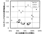
- liquid crystal display elements having spacer installation distances of 100 ⁇ m, 200 ⁇ m, and 400 ⁇ m, respectively, were prepared by changing the amount of liquid crystal supplied in the liquid crystal supply process step by step. The in-plane distribution of the cell gap in the display element was obtained.
- the cell size of the liquid crystal display element was 3.5 inches and the spacer size was 15 ⁇ .
- columnar spacers were formed using a photolithography method.
- FIG. 3 is a graph showing the relationship between the cell volume ratio of the amount of encapsulated liquid crystal (the amount of supplied liquid crystal) and the standard deviation serving as an index of the in-plane distribution of the cell gap.
- the cell volume ratio of the amount of encapsulated liquid crystal is the thickness of the liquid crystal layer in the liquid crystal display element. Corresponds to the ratio of the loaded spacer to the height.
- a vacuum bubble may be generated in the liquid crystal layer in a region where the cell volume ratio of the enclosed liquid crystal amount is 92% or less.
- the standard deviation of the in-plane distribution of the cell gap in the range of 98% or less was smaller than the value in the range of greater than 98%.
- the minimum value of the standard deviation of the in-plane distribution of the cell gap is shifted to the left side of the horizontal axis in FIG. 3 (the side where the cell volume ratio of the enclosed liquid crystal amount is lower).
- the liquid crystal display element having a spacer installation interval of 400 ⁇ m no vacuum bubbles were generated even in the region of 92% or less. This is considered to be due to the fact that the flexible substrate is bent more because the spacer installation interval is increased. Such a phenomenon is considered to be more remarkable in a liquid crystal display element having a larger spacer pitch.
- the standard deviation of the in-plane distribution of the cell gap is worse than that of the liquid crystal display element with the spacer installation interval of 100 or 200 ⁇ m. In all the measurements performed by changing the cell volume ratio, the value exceeds 0.1 ⁇ m.
- the standard deviation of the in-plane distribution of the cell gap of the liquid crystal display device fabricated in this example is about the thing exceeding 0.1 micrometer, when the display spot was confirmed visually, the clear spot was visually recognized.
- the spacer installation interval in the liquid crystal display element is less than 400 ⁇ m and the ratio of the thickness of the liquid crystal layer in the liquid crystal display element to the height of the unloaded spacer is 93 to 98%, the in-plane distribution of the cell gap It was revealed that can be kept good.
- the present invention can be widely used as a liquid crystal display element using a flexible substrate.
Landscapes
- Physics & Mathematics (AREA)
- Nonlinear Science (AREA)
- Mathematical Physics (AREA)
- Chemical & Material Sciences (AREA)
- Crystallography & Structural Chemistry (AREA)
- General Physics & Mathematics (AREA)
- Optics & Photonics (AREA)
- Liquid Crystal (AREA)
Abstract
Description
液晶表示素子10の概略的な構成について図1および図2を参照して以下に説明する。図1は、本実施形態の液晶表示素子10を示す断面図であり、図2は、その上面図である。なお、図1は、図2に示す液晶表示素子10のA‐A線矢視断面図である。
次に、本実施形態に係る液晶表示素子10の製造方法について説明する。
1a 前面基板
1b 背面基板
2 シール
3 液晶層
4 スペーサー
10 液晶表示素子
Claims (3)
- 少なくとも一方が可撓性を有する一対の基板と、
上記一対の基板間に封入された液晶層と、
上記一対の基板間に配置され、当該一対の基板間の間隙を保持する複数のスペーサーとを備え、
上記液晶層の厚みが、無荷重状態の上記スペーサーの、当該液晶層の厚み方向における高さに対して93~98%であり、
互いに隣接するスペーサーの間隔は400μm未満であることを特徴とする液晶表示素子。 - 請求項1に記載の液晶表示素子を備えることを特徴とする液晶表示装置。
- 少なくとも一方が可撓性を有する一対の基板と、上記一対の基板間に封入された液晶層と、上記一対の基板間に配置され、当該一対の基板間の間隙を保持するスペーサーとを備える液晶表示素子を製造する方法であって、
上記一対の基板のいずれか一方の基板に対して、複数のスペーサーを400μm未満のピッチで形成するスペーサー形成工程と、
上記スペーサー形成工程の後、上記液晶層の厚みが、無荷重状態の上記スペーサーの、当該液晶層の厚み方向における高さに対して93~98%になる量の液晶を、上記一対の基板間に封入する封入工程を含む液晶表示素子の製造方法。
Priority Applications (3)
| Application Number | Priority Date | Filing Date | Title |
|---|---|---|---|
| JP2012508113A JPWO2011122075A1 (ja) | 2010-03-31 | 2011-01-21 | 液晶表示素子及びその製造方法、ならびに液晶表示装置 |
| KR1020127028195A KR20120134147A (ko) | 2010-03-31 | 2011-01-21 | 액정 표시 소자 및 그 제조 방법, 및 액정 표시 장치 |
| US13/637,713 US20130021572A1 (en) | 2010-03-31 | 2011-01-21 | Liquid crystal display device element, method for manufacturing same, and liquid crystal display device |
Applications Claiming Priority (2)
| Application Number | Priority Date | Filing Date | Title |
|---|---|---|---|
| JP2010-083710 | 2010-03-31 | ||
| JP2010083710 | 2010-03-31 |
Publications (1)
| Publication Number | Publication Date |
|---|---|
| WO2011122075A1 true WO2011122075A1 (ja) | 2011-10-06 |
Family
ID=44711828
Family Applications (1)
| Application Number | Title | Priority Date | Filing Date |
|---|---|---|---|
| PCT/JP2011/051120 Ceased WO2011122075A1 (ja) | 2010-03-31 | 2011-01-21 | 液晶表示素子及びその製造方法、ならびに液晶表示装置 |
Country Status (4)
| Country | Link |
|---|---|
| US (1) | US20130021572A1 (ja) |
| JP (1) | JPWO2011122075A1 (ja) |
| KR (1) | KR20120134147A (ja) |
| WO (1) | WO2011122075A1 (ja) |
Cited By (1)
| Publication number | Priority date | Publication date | Assignee | Title |
|---|---|---|---|---|
| CN102692765A (zh) * | 2012-04-02 | 2012-09-26 | 友达光电股份有限公司 | 显示装置 |
Families Citing this family (1)
| Publication number | Priority date | Publication date | Assignee | Title |
|---|---|---|---|---|
| KR20150030105A (ko) | 2013-09-11 | 2015-03-19 | 삼성디스플레이 주식회사 | 액정 표시 장치 및 그 제조 방법 |
Citations (4)
| Publication number | Priority date | Publication date | Assignee | Title |
|---|---|---|---|---|
| JPH10325959A (ja) * | 1997-05-26 | 1998-12-08 | Semiconductor Energy Lab Co Ltd | 表示装置 |
| JPH11109372A (ja) * | 1997-09-30 | 1999-04-23 | Toshiba Electronic Engineering Corp | 液晶表示素子用基板の製造方法、液晶表示素子の製造方法、液晶表示素子用基板及び液晶表示素子 |
| JP2000147527A (ja) * | 1998-11-11 | 2000-05-26 | Minolta Co Ltd | 液晶光変調素子の製造方法 |
| JP2002357835A (ja) * | 2001-03-28 | 2002-12-13 | Toshiba Corp | 液晶表示モジュール |
Family Cites Families (3)
| Publication number | Priority date | Publication date | Assignee | Title |
|---|---|---|---|---|
| JP2003017259A (ja) * | 2001-06-29 | 2003-01-17 | Sanyo Electric Co Ltd | エレクトロルミネッセンス表示パネルの製造方法 |
| JP2004302297A (ja) * | 2003-03-31 | 2004-10-28 | Fujitsu Display Technologies Corp | 液晶表示パネル |
| EP2031438B1 (en) * | 2003-10-16 | 2010-10-06 | Sharp Kabushiki Kaisha | Substrate with spacer, panel, and method for producing panel |
-
2011
- 2011-01-21 WO PCT/JP2011/051120 patent/WO2011122075A1/ja not_active Ceased
- 2011-01-21 KR KR1020127028195A patent/KR20120134147A/ko not_active Ceased
- 2011-01-21 US US13/637,713 patent/US20130021572A1/en not_active Abandoned
- 2011-01-21 JP JP2012508113A patent/JPWO2011122075A1/ja active Pending
Patent Citations (4)
| Publication number | Priority date | Publication date | Assignee | Title |
|---|---|---|---|---|
| JPH10325959A (ja) * | 1997-05-26 | 1998-12-08 | Semiconductor Energy Lab Co Ltd | 表示装置 |
| JPH11109372A (ja) * | 1997-09-30 | 1999-04-23 | Toshiba Electronic Engineering Corp | 液晶表示素子用基板の製造方法、液晶表示素子の製造方法、液晶表示素子用基板及び液晶表示素子 |
| JP2000147527A (ja) * | 1998-11-11 | 2000-05-26 | Minolta Co Ltd | 液晶光変調素子の製造方法 |
| JP2002357835A (ja) * | 2001-03-28 | 2002-12-13 | Toshiba Corp | 液晶表示モジュール |
Cited By (1)
| Publication number | Priority date | Publication date | Assignee | Title |
|---|---|---|---|---|
| CN102692765A (zh) * | 2012-04-02 | 2012-09-26 | 友达光电股份有限公司 | 显示装置 |
Also Published As
| Publication number | Publication date |
|---|---|
| JPWO2011122075A1 (ja) | 2013-07-08 |
| KR20120134147A (ko) | 2012-12-11 |
| US20130021572A1 (en) | 2013-01-24 |
Similar Documents
| Publication | Publication Date | Title |
|---|---|---|
| KR101972881B1 (ko) | 액정표시장치 및 그 제조방법 | |
| JP5252337B2 (ja) | 表示デバイス装置、液晶表示装置及びその製造方法並びに製造装置 | |
| US20130016308A1 (en) | Liquid crystal display element, method for manufacturing same, and liquid crystal display device comprising the liquid crystal display element | |
| TWI480650B (zh) | 軟性顯示器及其製作方法 | |
| US9645455B2 (en) | Liquid crystal display panel, driving method and fabrication method thereof, and display device | |
| WO2010024006A1 (ja) | 有機エレクトロルミネセンスパネル、有機エレクトロルミネセンスディスプレイ、有機エレクトロルミネセンス照明、及び、それらの製造方法 | |
| TW200903120A (en) | Liquid crystal display device | |
| CN101644844B (zh) | 液晶显示面板 | |
| CN113015934A (zh) | 偏光片、显示面板及显示装置 | |
| WO2016074351A1 (zh) | 柔性液晶面板制作方法及柔性液晶面板 | |
| JP5281711B2 (ja) | 液晶表示素子及びその製造方法、ならびに液晶表示装置 | |
| EP3680708A1 (en) | Polarizer, display screen, terminal, and method for manufacturing polarizer | |
| WO2016163281A1 (ja) | 液晶表示装置及び液晶表示装置の製造方法 | |
| CN108519701B (zh) | 一种液晶移相器及其制作方法 | |
| WO2011122075A1 (ja) | 液晶表示素子及びその製造方法、ならびに液晶表示装置 | |
| US20070268446A1 (en) | Liquid crystal device and method for forming the same | |
| US20140024280A1 (en) | Method for making liquid crystal display module | |
| WO2022170744A1 (zh) | 一种偏光板、显示面板及其制备方法 | |
| CN113589414A (zh) | 光学膜片及其制备方法、背光模组及显示装置 | |
| JP5328176B2 (ja) | 液晶表示装置 | |
| TWM510466U (zh) | 具有光分配結構之偏振模組以及其液晶顯示器 | |
| KR101349784B1 (ko) | 기능성 패널 합착용 지지부재, 이를 구비한 표시소자 및 표시소자 제조방법 | |
| CN209992786U (zh) | 电致变色器件、壳体和电子设备 | |
| US9250467B2 (en) | Manufacturing mold and manufacturing method for color filter | |
| KR20110039892A (ko) | 백라이트 유닛의 제조방법 |
Legal Events
| Date | Code | Title | Description |
|---|---|---|---|
| 121 | Ep: the epo has been informed by wipo that ep was designated in this application |
Ref document number: 11762316 Country of ref document: EP Kind code of ref document: A1 |
|
| WWE | Wipo information: entry into national phase |
Ref document number: 2012508113 Country of ref document: JP |
|
| WWE | Wipo information: entry into national phase |
Ref document number: 13637713 Country of ref document: US |
|
| NENP | Non-entry into the national phase |
Ref country code: DE |
|
| ENP | Entry into the national phase |
Ref document number: 20127028195 Country of ref document: KR Kind code of ref document: A |
|
| 122 | Ep: pct application non-entry in european phase |
Ref document number: 11762316 Country of ref document: EP Kind code of ref document: A1 |