WO2011121845A1 - 照明装置、および植物栽培装置 - Google Patents
照明装置、および植物栽培装置 Download PDFInfo
- Publication number
- WO2011121845A1 WO2011121845A1 PCT/JP2010/071276 JP2010071276W WO2011121845A1 WO 2011121845 A1 WO2011121845 A1 WO 2011121845A1 JP 2010071276 W JP2010071276 W JP 2010071276W WO 2011121845 A1 WO2011121845 A1 WO 2011121845A1
- Authority
- WO
- WIPO (PCT)
- Prior art keywords
- light
- lens
- fixing plate
- plant
- led
- Prior art date
- Legal status (The legal status is an assumption and is not a legal conclusion. Google has not performed a legal analysis and makes no representation as to the accuracy of the status listed.)
- Ceased
Links
Images




Classifications
-
- F—MECHANICAL ENGINEERING; LIGHTING; HEATING; WEAPONS; BLASTING
- F21—LIGHTING
- F21V—FUNCTIONAL FEATURES OR DETAILS OF LIGHTING DEVICES OR SYSTEMS THEREOF; STRUCTURAL COMBINATIONS OF LIGHTING DEVICES WITH OTHER ARTICLES, NOT OTHERWISE PROVIDED FOR
- F21V5/00—Refractors for light sources
- F21V5/007—Array of lenses or refractors for a cluster of light sources, e.g. for arrangement of multiple light sources in one plane
-
- A—HUMAN NECESSITIES
- A01—AGRICULTURE; FORESTRY; ANIMAL HUSBANDRY; HUNTING; TRAPPING; FISHING
- A01G—HORTICULTURE; CULTIVATION OF VEGETABLES, FLOWERS, RICE, FRUIT, VINES, HOPS OR SEAWEED; FORESTRY; WATERING
- A01G7/00—Botany in general
- A01G7/04—Electric or magnetic or acoustic treatment of plants for promoting growth
- A01G7/045—Electric or magnetic or acoustic treatment of plants for promoting growth with electric lighting
-
- A—HUMAN NECESSITIES
- A01—AGRICULTURE; FORESTRY; ANIMAL HUSBANDRY; HUNTING; TRAPPING; FISHING
- A01G—HORTICULTURE; CULTIVATION OF VEGETABLES, FLOWERS, RICE, FRUIT, VINES, HOPS OR SEAWEED; FORESTRY; WATERING
- A01G9/00—Cultivation in receptacles, forcing-frames or greenhouses; Edging for beds, lawn or the like
- A01G9/24—Devices or systems for heating, ventilating, regulating temperature, illuminating, or watering, in greenhouses, forcing-frames, or the like
- A01G9/249—Lighting means
-
- F—MECHANICAL ENGINEERING; LIGHTING; HEATING; WEAPONS; BLASTING
- F21—LIGHTING
- F21V—FUNCTIONAL FEATURES OR DETAILS OF LIGHTING DEVICES OR SYSTEMS THEREOF; STRUCTURAL COMBINATIONS OF LIGHTING DEVICES WITH OTHER ARTICLES, NOT OTHERWISE PROVIDED FOR
- F21V17/00—Fastening of component parts of lighting devices, e.g. shades, globes, refractors, reflectors, filters, screens, grids or protective cages
- F21V17/002—Fastening of component parts of lighting devices, e.g. shades, globes, refractors, reflectors, filters, screens, grids or protective cages with provision for interchangeability, i.e. component parts being especially adapted to be replaced by another part with the same or a different function
-
- F—MECHANICAL ENGINEERING; LIGHTING; HEATING; WEAPONS; BLASTING
- F21—LIGHTING
- F21V—FUNCTIONAL FEATURES OR DETAILS OF LIGHTING DEVICES OR SYSTEMS THEREOF; STRUCTURAL COMBINATIONS OF LIGHTING DEVICES WITH OTHER ARTICLES, NOT OTHERWISE PROVIDED FOR
- F21V17/00—Fastening of component parts of lighting devices, e.g. shades, globes, refractors, reflectors, filters, screens, grids or protective cages
- F21V17/10—Fastening of component parts of lighting devices, e.g. shades, globes, refractors, reflectors, filters, screens, grids or protective cages characterised by specific fastening means or way of fastening
- F21V17/12—Fastening of component parts of lighting devices, e.g. shades, globes, refractors, reflectors, filters, screens, grids or protective cages characterised by specific fastening means or way of fastening by screwing
-
- F—MECHANICAL ENGINEERING; LIGHTING; HEATING; WEAPONS; BLASTING
- F21—LIGHTING
- F21Y—INDEXING SCHEME ASSOCIATED WITH SUBCLASSES F21K, F21L, F21S and F21V, RELATING TO THE FORM OR THE KIND OF THE LIGHT SOURCES OR OF THE COLOUR OF THE LIGHT EMITTED
- F21Y2105/00—Planar light sources
- F21Y2105/10—Planar light sources comprising a two-dimensional [2D] array of point-like light-generating elements
-
- F—MECHANICAL ENGINEERING; LIGHTING; HEATING; WEAPONS; BLASTING
- F21—LIGHTING
- F21Y—INDEXING SCHEME ASSOCIATED WITH SUBCLASSES F21K, F21L, F21S and F21V, RELATING TO THE FORM OR THE KIND OF THE LIGHT SOURCES OR OF THE COLOUR OF THE LIGHT EMITTED
- F21Y2115/00—Light-generating elements of semiconductor light sources
- F21Y2115/10—Light-emitting diodes [LED]
-
- Y—GENERAL TAGGING OF NEW TECHNOLOGICAL DEVELOPMENTS; GENERAL TAGGING OF CROSS-SECTIONAL TECHNOLOGIES SPANNING OVER SEVERAL SECTIONS OF THE IPC; TECHNICAL SUBJECTS COVERED BY FORMER USPC CROSS-REFERENCE ART COLLECTIONS [XRACs] AND DIGESTS
- Y02—TECHNOLOGIES OR APPLICATIONS FOR MITIGATION OR ADAPTATION AGAINST CLIMATE CHANGE
- Y02A—TECHNOLOGIES FOR ADAPTATION TO CLIMATE CHANGE
- Y02A40/00—Adaptation technologies in agriculture, forestry, livestock or agroalimentary production
- Y02A40/10—Adaptation technologies in agriculture, forestry, livestock or agroalimentary production in agriculture
- Y02A40/25—Greenhouse technology, e.g. cooling systems therefor
-
- Y—GENERAL TAGGING OF NEW TECHNOLOGICAL DEVELOPMENTS; GENERAL TAGGING OF CROSS-SECTIONAL TECHNOLOGIES SPANNING OVER SEVERAL SECTIONS OF THE IPC; TECHNICAL SUBJECTS COVERED BY FORMER USPC CROSS-REFERENCE ART COLLECTIONS [XRACs] AND DIGESTS
- Y02—TECHNOLOGIES OR APPLICATIONS FOR MITIGATION OR ADAPTATION AGAINST CLIMATE CHANGE
- Y02P—CLIMATE CHANGE MITIGATION TECHNOLOGIES IN THE PRODUCTION OR PROCESSING OF GOODS
- Y02P60/00—Technologies relating to agriculture, livestock or agroalimentary industries
- Y02P60/14—Measures for saving energy, e.g. in green houses
Definitions
- the present invention relates to a lighting device for plant cultivation and a plant cultivation device equipped with the same.
- Lighting devices using light emitting diodes (LEDs) as light sources have recently been used in various fields. As an example, it has been proposed to use an LED lighting device as an artificial light source for a plant factory or a plant cultivation apparatus for cultivating plants such as vegetables indoors.
- LEDs light emitting diodes
- the LED is not only efficient as an illumination light source for plants in that only light having a wavelength necessary for plants can be freely selected, but also conventional lamps such as incandescent lamps, fluorescent lamps, metal halide lamps, and high-pressure sodium lamps. It is very advantageous as a light source for plant cultivation because it does not contain infrared rays and heat rays contained in a large amount in the light source. In other words, in the conventional light source, direct illumination from the vicinity of the cultivated plant is impossible in order to avoid troubles such as leaf burning by heat rays (that is, an expensive and large space heat removal device is required), and the light utilization efficiency Was disadvantageous.
- Patent Documents 1 to 3 propose a technique of using an illumination device using LEDs as a light source for plant cultivation.
- the LED light source does not generate heat rays unlike the conventional light source, but a part of the input electric power is not converted into light, leading to a temperature rise (that is, heat generation) of the LED element itself. .
- Such heat generation of the LED may reach about 40 ° C. to 80 ° C. at the surface temperature of the LED package, which is not preferable for plant cultivation.
- the temperature rise of the LED element is not preferable because it leads to deterioration of performance for the LED element itself. Therefore, it is desired to take some measures to dissipate heat from the LED element and the LED substrate.
- Patent Document 1 proposes a plant cultivation apparatus that includes a panel-shaped LED light source and a cooling device for cooling the LED.
- power consumption can be suppressed by using the LED as a light source, and a temperature rise of the LED itself is suppressed by providing a cooling device.
- Japanese Patent Publication “JP 9-98665 A (published on April 15, 1997)” Japanese Patent Publication “JP 2005-185823 (July 14, 2005)” Japanese Patent Publication “Japanese Patent Laid-Open No. 2008-142030 (published on June 26, 2008)”
- a conventional lighting device using an LED as a light source does not have a configuration in which the intensity distribution in each direction of light emitted from the LED (these are referred to as “light distribution” of the LED) can be adjusted.
- the present invention has been made in view of the above problems, and an object of the present invention is to provide an illuminating device for plant cultivation that has been improved from the viewpoints of heat generation control of LED and light distribution adjustment of LED.
- an illumination device that irradiates light to a plant, and includes a light-emitting diode as a light source, a substrate on which the light-emitting diodes are arranged, and the substrate. And an optical member that changes the optical path of the irradiation light from the light-emitting diode, and the optical member is attached to the apparatus in a state where it can be attached and detached. It is characterized by being.
- an optical member that can change the optical path of light from the light emitting diode is attached to the device in a detachable state.
- “changing the optical path” means changing the irradiation range and irradiation direction of light from the state emitted from the light source.
- the expression “changing the light path of the light emitting diode” can be rephrased as “adjusting the light distribution of the light emitting diode”.
- the irradiation range and irradiation direction of the light irradiated from the light emitting diode can be changed by replacing optical members having different characteristics according to the purpose. Therefore, according to the illuminating device of the present invention, it is possible to perform efficient light irradiation according to the type of plant to be irradiated and the growth state.
- an optical member is provided between the plant and the substrate on which the light emitting diodes are arranged.
- it can be set as the structure where the heat which generate
- the optical member absorbs heat generated from the surface of the light emitting diode and the substrate, and can be efficiently radiated. Therefore, the cooling effect of the light emitting diode can be further enhanced as compared with the conventional configuration in which only the cooling plate is provided on the back surface of the substrate.
- the optical member is provided between the plant and the light emitting diode installation substrate, the area in contact with the outside air on the substrate on which the light emitting diode is mounted is reduced. For this reason, even if a temperature difference occurs between the space where the plant is placed and the light emitting diode, and the condensation occurs, the substrate is not easily cooled by the outside air, and the light emitting diode is less likely to cause the condensation. it can. Therefore, the light emitting diode is not damaged by condensation, and the reliability of the light emitting diode can be improved and the life of the light emitting diode can be extended.
- the plant cultivation apparatus according to the present invention includes any one of the above-described lighting apparatuses.
- the plant cultivation apparatus of the present invention can change the irradiation range and irradiation direction of the light emitted from the light emitting diode according to the purpose. Moreover, in the plant cultivation apparatus of this invention, it can be set as the structure where the heat
- the optical member is provided between the plant and the light emitting diode installation substrate, so that a temperature difference occurs between the space where the plant is disposed and the light emitting diode, thereby causing dew condensation. Even when this occurs, the light-emitting diode can have a structure in which condensation does not easily occur. Therefore, the light emitting diode is not damaged by condensation, and the reliability of the light emitting diode can be improved and the life of the light emitting diode can be extended.
- the light distribution adjustment of the light emitting diode can be easily performed by replacing the optical member according to the application. Further, by providing an optical member between the light emitting die auto and the plant, it is possible to realize a structure in which the plant is not easily affected by the heat generated by the light emitting diode and a structure in which condensation is unlikely to occur in the light emitting diode.
- FIG. (A)-(d) is sectional drawing which shows the specific example of the structure of the lens with which the illuminating device concerning one embodiment of this invention was equipped.
- FIG. 11B is a plan view of a lens fixing plate and a heat conductive sheet provided in the lighting device shown in FIG. 10.
- C is sectional drawing which expands and shows a part of illuminating device shown to (a) further.
- FIGS. 1 to 9 An embodiment of the present invention will be described with reference to FIGS. 1 to 9 as follows. However, the dimensions, materials, shapes, relative arrangements, and the like of the components described in this embodiment are not intended to limit the scope of the present invention only to those unless otherwise specified. This is just an example.
- the plant cultivation device 10 is configured by a rectangular parallelepiped case 11, and an illumination device 12 is provided on the upper surface of the case 11.
- the plant 31 is placed on the bottom surface of the case 11, and light is irradiated from the lighting device 12 provided on the top surface.
- the shape of the case 11 is not limited to a rectangular parallelepiped shape as shown in FIG. Examples of other shapes include a shape like a shelf composed of a plurality of stages, a cylindrical shelf, a doll bed, and the like.
- the arrangement position of the lighting device 12 is not necessarily limited to the upper surface, and it is only necessary that the plant placed in the case 11 can be irradiated with light.
- FIG. 1 the perspective view of the illuminating device 12 is shown.
- the illuminating device 12 is shown in a state that is upside down from the state provided in the plant cultivation device 10.
- FIG. 3 the respective constituent members constituting the lighting device 12 are disassembled and shown.
- FIG. 4 one lens part of the illuminating device 12 is expanded and shown.
- an LED substrate 22 (substrate) and a lens fixing plate 24 (fixing plate, optical member) are sequentially stacked on a cooling plate 21.
- the cooling plate 21 is provided on the back side of the LED substrate 22 (the side opposite to the side on which the plant is placed), and can absorb the heat generated from the LED chip 23 (light emitting diode) during light irradiation.
- the structure similar to the cooling plate used for the conventional illuminating device for plant cultivation is employable.
- any heat can be used as long as heat from the LED is transmitted to the cooling plate through the substrate and heat can be dissipated by heat transfer by heat conduction.
- the cooling plate include an aluminum plate and a copper plate. Further, not only a plate but also an air cooling device, a water cooling device, or the like formed of a plate made of aluminum, copper or the like can be used instead of the cooling plate.
- the LED substrate 22 has a configuration in which a plurality of LED chips 23 (LED packages) are arranged on a substrate 22a (for example, an insulating substrate).
- the LED chip 23 can employ the same configuration as the LED chip used in a conventional lighting device for plant cultivation. That is, the LED chip 23 can use a general-purpose product. Note that some normal LED chips (LED packages) have a lens. However, in the present invention, since a lens is separately attached as described later, a package without a lens is used. It is preferable to use it.
- each LED chip may emit light of the same color, or may be composed of a plurality of types of LED chips that emit light of different wavelengths.
- FIG. 5 shows an example of a method for arranging a plurality of LED chips 23 on the LED substrate 22.
- two LEDs of the same type constitute one unit 23d, and this unit is repeatedly arranged vertically and horizontally.
- the lens fixing plate 24 is provided with holes 24 a in accordance with the LED chips 23 arranged on the LED substrate 22. Thereby, as shown in FIG. 4, when the lens fixing plate 24 and the LED substrate 22 are overlapped, each LED chip 23 is disposed in each hole 24a.
- a metal having high thermal conductivity and reflectivity is used as the material for the lens fixing plate 24. More specifically, aluminum, copper, or the like can be used.
- a lens 25 optical path changing unit, optical member for adjusting the optical path of the irradiation light from the LED is fitted.
- the lens 25 is for adjusting the traveling direction and irradiation range (that is, LED light distribution) of the light emitted from the LED chip 23.
- the light distribution of this LED can be adjusted by appropriately changing the shape of the lens 25 in accordance with Snell's law. Specifically, by changing the curvature of the curved surface of the projection of the lens 25 having a convex shape, the light path of the light emitted from the LED chip 23 is changed to the light of the LED substrate 22 as shown by the arrow A in FIG. It can be bent in a direction perpendicular to the exit surface.
- the above-mentioned “adjust by changing the shape of the lens 25 according to Snell's law” means that, for example, in the case of a convex lens, the light that meets the total reflection condition of light on the convex surface is gathered inward. On the other hand, in the case of a concave lens, this means that light that meets the conditions for total reflection of light on the concave surface is emitted in a direction that spreads outward.
- the light distribution of the LED can be adjusted by utilizing such characteristics of the lens.
- Examples of the material of the lens 25 include transparent resins such as (meth) acrylic resin, COP (cycloolefin polymer), COC (cycloolefin copolymer), and polycarbonate.
- Specific examples of the (meth) acrylic resin include PMMA (methyl methacrylate resin).
- Specific examples of COP (cycloolefin polymer) include “ZEONOR” (registered trademark, manufactured by Nippon Zeon Co., Ltd.).
- the plant to be irradiated with light with respect to the illumination device 12 having such a configuration is placed on the LED substrate 22 on the side where the lens fixing plate 24 is disposed. That is, the lens fixing plate 24 is provided on the light emitting surface side of the LED substrate 22, and the cooling plate 21 is provided on the back surface side of the light emitting surface.
- the lens fixing plate 24 formed of a material having high thermal conductivity is the LED substrate 22.
- the plant 31 to be irradiated with light is absorbed by the lens fixing plate 24 and can be efficiently radiated. Therefore, the cooling effect of the LED chip can be further enhanced as compared with the configuration of only the cooling plate 21.
- the lens 25 and the lens fixing plate 24 are separate constituent members, and each lens 25 is attached to and detached from the hole 24a formed in the lens fixing plate 24. Is configured to be fitted in a possible state. Thereby, it becomes possible to replace
- a separate lens 25 can be attached to each individual LED chip 23. In the case of such a configuration, the light distribution of each LED chip 23 can be individually controlled.
- a lens fixing plate 24 and a lens 25 are provided between the LED chip 23 and the plant 31.
- the LED chip 23 is covered with the lens 25 and the lens fixing plate 24, and is not contacting the space where the plant 31 is arrange
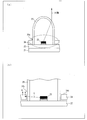
- FIG. 6A shows a cross-sectional configuration of one lens 25 portion of the illuminating device 12, and FIG. 6B further shows an enlarged portion surrounded by a broken line in FIG.
- a metal having a high reflectance is used as the material of the lens fixing plate 24. Therefore, the surface of the lens fixing plate 24 functions as a reflecting plate, and as shown in FIG. 6B, the light emitted from the LED chip 23 in the lateral direction (direction along the light irradiation surface of the illumination device 12) is The light is reflected at the side surface 24b of the hole 24a formed in the lens fixing plate 24 (see arrow B in FIG. 6B). Thereby, the light leak of the LED chip 23 to the said horizontal direction can be reduced, and the light from an LED chip can be irradiated to a plant more efficiently.
- a reflection sheet having a higher reflectance may be attached to the side surface 24b of the hole 24a formed in the lens fixing plate 24 (that is, the contact surface 24b with the lens 25). it can.
- the light leakage of the LED chip 23 in the lateral direction can be reduced, the light emission from each LED chip 23 becomes independent. Therefore, if a lighting method that partially controls the amount of light emission, such as local dimming that is used in backlights of liquid crystal display devices, is applied to the lighting device of the present invention, different characteristics (light quantity, wavelength) Etc.) can be selectively irradiated.
- the cooling plate 21 is abbreviate
- the lens fixing plate 24 and the LED substrate 22 are arranged very close to each other (substantially in contact), but in the structure shown in FIG. 7, the lens fixing plate 24 and the LED substrate are arranged. 22 are arranged at a predetermined distance from each other.
- FIG. 7A is an example of a configuration in which one lens 25a is provided for one LED chip 23.
- the lens 25a shown in this figure has a peripheral diameter of its bottom surface portion (contact portion with the LED substrate 22) larger than other portions.
- each LED chip 23 on the LED substrate 22 is covered with the lens 25a, and then the lens fixing plate 24 is covered, and the lens 25a is fixed by pressing the bottom surface of each lens 25a.
- FIG. 7B is a single member in which a plurality of lens protrusions 26 are connected. Also in this configuration, substantially like FIG. 7A, after placing each LED chip 23 on the LED substrate 22 so as to cover each protrusion 26 of the lens 25b, the lens fixing plate 24 is covered, The lens 25b is fixed by pressing the connecting portion between the protrusions 26.
- the peripheral diameter of the bottom surface portion (portion inserted into the hole 24a) is smaller than other portions.
- the lens 25c is individually fixed by inserting the bottom surface portion of the lens 25c into the hole 24a of the lens fixing plate 24.
- the lens 25d shown in (d) of FIG. 7 is a single member formed by connecting a plurality of lens protrusions 26, similarly to the lens 25b shown in (b) of FIG.
- this lens 25d as shown in FIG. 7D, after the lens fixing plate 24 is placed on the LED substrate 22, the bottom surface portion of each protrusion 26 of the lens 25d is fitted into each hole 24a. Then, screws 27 are inserted so as to penetrate the lens 25 d and the lens fixing plate 24, and the lens 25 d is fixed to the LED substrate 22.
- the lens 25 can be exchanged with respect to the LED substrate 22, and can be changed to a lens 25 having a different shape depending on the use of the plant cultivation apparatus 10.
- one lens (optical member) formed by connecting a plurality of lens protrusions 26 is provided on the entire surface of one LED substrate 22.
- the structure which is provided may be sufficient and one LED board 22 may be provided with two or more structures. In a configuration in which one lens is provided for one LED substrate 22, the lenses on the entire substrate can be exchanged at one time.
- the lens fixing plate is also divided according to each lens.
- the light irradiation surface of the illuminating device can be divided into a plurality of regions to which different lenses are attached, and the lenses can be individually exchanged for each region.
- FIG. 8A and 8B show an example in which the lens 25 is exchanged according to the growth of the plant 31.
- FIG. FIG. 8A shows an example of the illumination device 12 when the plant 31 is just germinated in the plant cultivation device 10.
- FIG.8 (b) an example of the illuminating device 12 after the plant 31 shown to (a) of FIG. 8 grew is shown.
- the cooling plate 21 is omitted.
- the lens 25e has a deeper bottom than the lens 25f.
- the light L1 from the LED light source irradiated through the deep lens 25e has a relatively narrow irradiation range and a relatively high light intensity. That is, light with high intensity is emitted toward the direction directly below the LED chip 23. Thereby, light can be efficiently irradiated to the small plant 31 that has just germinated.
- the lens 25f attached to the illumination device 12 after the plant has grown has a shallower shape than the lens 25e.
- the light L2 from the LED light source irradiated through the shallow lens 25f at the bottom is irradiated over a wider range than the light L2. Thereby, it is possible to irradiate light uniformly to the plant 31 that has grown greatly.
- the shape of the lens 25 can be changed according to the growth state of the plant.
- the light environment more suitable for the growth degree of the plant 31 can be created.
- the lens 25e is used when cultivating the plant 31 that has just germinated, although it is preferable to use the lens 25f at the time of cultivation of the plant 31 after growing, the present invention is not limited to this. That is, the lens used in the plant cultivation apparatus of the present invention may be selected from lenses that can create an optimal light environment according to the type and growth state of the plant.
- the structure that one lens 25g is provided with respect to several LED chip 23 is also possible.
- a lens 25g is used, for example, as shown in FIG. 8C, the irradiation light L3 from the three LED chips 23 can be condensed near the center thereof. Therefore, it is possible to concentrate and irradiate light on the place where the plant 31 is growing.
- the lens fixing plate 24 also needs to be replaced according to the shape of the lens.
- lens fixing plate 24 provided in the illumination device 12 described above is formed of a metal material
- the present invention is not limited to this.
- the material of the lens fixing plate for example, the same material as that of the light guide plate used for the backlight of the liquid crystal display panel can be used.
- FIG. 9A shows a cross-sectional configuration of one lens 25 portion of the illuminating device 12 when the lens fixing plate 34 is formed of a light guide plate, and FIG. The portion surrounded by the broken line is further enlarged and shown.
- the material for the lens fixing plate 34 in this case include transparent resins such as (meth) acrylic resin, COP (cycloolefin polymer), COC (cycloolefin copolymer), and polycarbonate. These transparent resins are the same as the materials suitable for the lens 25 described above. However, the present invention is not limited to this, and any material that can transmit light while propagating may be used.
- the light guide plate When the light guide plate is used as the material of the lens fixing plate 34 as described above, the light is emitted from the LED chip 23 in the lateral direction (the direction along the light irradiation surface of the illumination device 12) as shown in FIG.
- the emitted light propagates through the lens fixing plate 34 (see arrow C in FIG. 9B) and is emitted from the surface 34b (light irradiation surface) of the lens fixing plate 34 (see FIG. 9B).
- Arrow D Thereby, since light can be emitted also from a region where the LED chip 23 is not arranged, unevenness in light and darkness of the entire illumination device 12 can be reduced. Moreover, even if the number of LED chips 23 is reduced, relatively uniform light can be irradiated, so that the cost can be reduced.
- the LED chip 23 is covered with the lens 25 and the lens fixing plate 34, and thus is in contact with the space in which the plant 31 is disposed. Absent. Therefore, as in the case where the lens fixing plate is made of metal, the LED chip 23 is not damaged by condensation, and the reliability of the LED chip 23 can be improved and the life of the LED chip 23 can be increased. Can be extended. However, since the light guide plate has a lower thermal conductivity than a metal, the cooling effect is less than that of the lens fixing plate 24 formed of a metal material.
- the material for the lens fixing plate may be a high thermal conductive resin.
- the high thermal conductive resin a commercially available “high thermal conductive resin” can be used.
- Specific examples of the high thermal conductive resin include high thermal conductive PPS (polyphenylene sulfide resin).
- a sheet obtained by blending and designing a polymer such as acrylic or silicon and a heat conductive filler can be used as a lens fixing plate made of a high heat conductive resin.
- the lens fixing plate 24 absorbs heat generated from the LED chip and can efficiently dissipate heat. Therefore, the cooling effect of the LED chip can be enhanced.
- the LED chip in the horizontal direction can be obtained by attaching a reflective sheet having a higher reflectance to the side surface of the hole 34a formed in the lens fixing plate 34 (that is, the contact surface with the lens 25). 23 light leakage can be reduced, and the light from the LED chip can be irradiated to the plant more efficiently.
- the reflection sheet may be provided on a surface of the lens fixing plate 34 opposite to the light irradiation surface 34b. Thereby, light can be more efficiently emitted to the light irradiation surface 34b side.
- a configuration in which a reflection portion having a predetermined shape (for example, dot shape) is partially printed on the surface can be employed. .
- the external appearance of the plant cultivation apparatus 10 according to the present embodiment is as shown in FIG.
- the plant cultivation apparatus 10 is provided with the illumination device 42 according to the present embodiment.
- FIG. 10 the perspective view of the illuminating device 42 is shown.
- the illuminating device 42 is shown in a state that is upside down from the state provided in the plant cultivation device 10.
- FIG. 11 each structural member which comprises the illuminating device 42 is decomposed
- FIG. 12A one lens portion of the illumination device 42 is shown enlarged.
- the LED substrate 52 (substrate), the heat conductive sheet 56, and the lens fixing plate 54 (fixing plate, optical member) are arranged in this order on the cooling plate 51. It is piled up.
- the cooling plate 51 is provided on the back side of the LED substrate 52 and can absorb the heat generated from the LED chip 53 during light irradiation.
- the LED substrate 52 has a configuration in which a plurality of LED chips 53 (LED packages) are arranged on a substrate 52a (for example, an insulating substrate).
- the LED chip 53 (light emitting diode) can adopt the same configuration as the LED chip 23 of the first embodiment.
- each LED chip may emit light in the same color, or may be composed of a plurality of types of LED chips that emit light of different wavelengths.
- the lens fixing plate 54 has holes 54 a formed in accordance with the LED chips 53 arranged on the LED substrate 52. Accordingly, as shown in FIG. 12A, when the lens fixing plate 54 and the LED substrate 52 are overlapped, the LED chips 53 are arranged in the portions of the holes 54a.
- the lens fixing plate 54 is formed of a resin having a light guide property (light propagation property). That is, like the lens fixing plate 34 shown in FIG. 9, it is formed of a light guide plate. More specifically, the lens fixing plate 54 can be formed of a transparent resin such as (meth) acrylic resin, COP (cycloolefin polymer), COC (cycloolefin copolymer), or polycarbonate.
- a heat conductive sheet 56 is provided between the LED substrate 52 and the lens fixing plate 54 in addition to the above-described plates.
- holes 56 a are formed in the heat conductive sheet 56 according to the LED chips 53 arranged on the LED substrate 52.
- each LED chip 53 will be arrange
- the material of the heat conductive sheet 56 include a heat conductive olefin compound. Specific examples include thermal conductive sheets manufactured by Furukawa Electric Co., Ltd. or Electrochemical Industry Co., Ltd., but are not limited thereto.
- FIG. 12B shows the planar configuration of a part of the lens fixing plate 54 and the heat conductive sheet 56, respectively, and the cross-sectional configuration of the XX ′ line portion shown in FIG. This is shown in FIG.
- the lens 55 in each hole 54a and 56a formed in the lens fixing plate 54 and the heat conductive sheet 56, the lens 55 (in order to adjust the optical path of the irradiation light from LED) An optical path changing unit and an optical member) are fitted. That is, the lens 55 is disposed on the LED substrate 52 through the lens fixing plate 54 and the heat conductive sheet 56. The lens 55 is for adjusting the intensity distribution in each direction of the light emitted from the LED chip 53 (that is, the light distribution of the LED).
- the light distribution of this LED can be adjusted by appropriately changing the shape of the lens 55 in accordance with Snell's law. Specifically, the curvature of the curved surface of the projection of the lens 55 having a convex shape is changed, and the optical path of light emitted from the LED chip 53 is changed to an LED as indicated by an arrow A in FIG.
- the substrate 52 can be bent in a direction perpendicular to the light exit surface.
- the same material as the lens 25 of the first embodiment can be applied.
- FIG. 12 is a cross-sectional view showing a part of the illumination device shown in (a) of FIG. Note that a part of the lighting device illustrated in FIG. 12C is a portion surrounded by a broken line in FIG. This portion corresponds to the cross section of the X-X ′ line portion in the lens fixing plate 54 and the heat conductive sheet 56 shown in FIG.
- the illumination device 42 of the present embodiment is provided with a lens fixing plate 54 formed of a material having light propagation performance on the outermost surface of a laminated structure composed of a plurality of plates. It has been. Therefore, the light emitted from the LED chip 53 in the lateral direction (the direction along the light irradiation surface of the illumination device 42) propagates through the lens fixing plate 54 (see arrow B in FIG. 12C), and the lens. The light is emitted from the surface 54b of the fixed plate 54 (arrow C in FIG. 12C). Thereby, since light can be emitted also from the region where the LED chip 53 is not disposed, the brightness unevenness of the entire illumination device 42 can be reduced. Further, even if the number of LED chips 53 is reduced, relatively uniform light can be irradiated, so that the cost can be reduced.
- the heat conductive sheet 56 formed of a material having high heat conductivity includes the LED substrate 52 and the light. It arrange
- the lens 55 and the lens fixing plate 54 are separate constituent members, and each lens 55 is attached to and detached from a hole 54a formed in the lens fixing plate 54. It is configured to be fitted in a possible state. Thereby, it becomes possible to replace
- a lens fixing plate 54 and a lens 55 are provided between the LED chip 53 and the plant 31.
- the LED chip 53 is covered with the lens 55 and the lens fixing plate 54, and is not contacting the space where the plant 31 is arrange
- an illumination device that irradiates light to a plant, and includes a light-emitting diode as a light source, a substrate on which the light-emitting diodes are arranged, and the substrate. And an optical member that changes the optical path of the irradiation light from the light-emitting diode, and the optical member is attached to the apparatus in a state where it can be attached and detached. It is characterized by being.
- an optical member that can change the optical path of light from the light emitting diode is attached to the device in a detachable state.
- “changing the optical path” means changing the irradiation range and irradiation direction of light from the state emitted from the light source.
- the expression “changing the light path of the light emitting diode” can be rephrased as “adjusting the light distribution of the light emitting diode”.
- the irradiation range and irradiation direction of the light irradiated from the light emitting diode can be changed by replacing optical members having different characteristics according to the purpose. Therefore, according to the illuminating device of the present invention, it is possible to perform efficient light irradiation according to the type of plant to be irradiated and the growth state.
- an optical member is provided between the plant and the substrate on which the light emitting diodes are arranged.
- it can be set as the structure where the heat which generate
- the optical member absorbs heat generated from the surface of the light emitting diode and the substrate, and can be efficiently radiated. Therefore, the cooling effect of the light emitting diode can be further enhanced as compared with the conventional configuration in which only the cooling plate is provided on the back surface of the substrate.
- the optical member is provided between the plant and the light emitting diode installation substrate, the area in contact with the outside air on the substrate on which the light emitting diode is mounted is reduced. For this reason, even if a temperature difference occurs between the space where the plant is placed and the light emitting diode, and the condensation occurs, the substrate is less likely to be cooled by the outside air and the light emitting diode is less likely to cause the condensation. it can. Therefore, the light emitting diode is not damaged by condensation, and the reliability of the light emitting diode can be improved and the life of the light emitting diode can be extended.
- the optical member includes an optical path changing unit and a fixing plate for fixing the optical path changing unit, and the fixing plate is disposed on the substrate. And the optical path changing portion may be attached to the hole.
- the optical path changing unit it is possible to change only the optical path changing unit to a different type with the fixed plate attached to the apparatus. Therefore, it is possible to easily adjust the irradiation light from the light emitting diode to a desired light distribution state according to the growth state of the plant, the kind of the plant, and the like.
- the light-emitting diode provided on the substrate is cut off from the space where the plant is arranged by fitting the optical path changing unit such as a lens into the hole formed in the fixed plate. Will be. For this reason, even if condensation occurs due to a temperature difference between the space where the plant is placed and the light emitting diode, the surface of the fixed plate and the optical path changing unit (the boundary with the space where the plant is placed) In the light emitting diode, no condensation occurs. Therefore, the light emitting diode is not damaged by condensation, and the reliability of the light emitting diode can be improved and the life of the light emitting diode can be extended.
- one or a plurality of light emitting diodes may be used as one unit, and one optical path changing unit may be provided for each unit.
- the optical path changing unit can be changed for each unit composed of one or a plurality of light emitting diodes. Therefore, the optical path of the irradiation light from a light emitting diode can be varied according to the position where the light emitting diode is provided. Within the same lighting device, the characteristics of irradiation light (irradiation range, irradiation direction, etc.) can be adjusted for each region in accordance with the state of the plant to be irradiated.
- the optical member is composed of a plurality of members, and may be attached to the device in a state in which attachment and removal are possible for each constituent member.
- the light irradiation surface of the lighting device can be divided into a plurality of regions to which different components are attached, and the optical member can be individually replaced for each region.
- the fixing plate may be formed of a metal material.
- the fixing plate provided between the plant and the substrate on which the light emitting diode is installed is formed of the metal material having high thermal conductivity, so that the heat generated from the light emitting diode is heated.
- the conductive sheet absorbs and can efficiently dissipate heat. Therefore, the cooling effect of the light emitting diode can be further enhanced.
- the fixing plate may be formed of a resin having a light guide property.
- the light emitted from the light emitting diode can be efficiently emitted to the side on which the plant is placed while propagating through the resin having a light guide property.
- light having a relatively high intensity can be emitted from a region on the substrate where the light emitting diodes are not arranged. Therefore, even when the number of light emitting diodes is reduced, light having a uniform or wide irradiation range can be obtained.
- An illumination device that can irradiate can be realized.
- the fixing plate may have a configuration in which a reflective sheet is further attached to the light-guiding resin.
- the light emitted from the light emitting diode is propagated through the resin having light guide property, and the light is efficiently emitted to the side on which the plant is placed by the reflection action of the reflection sheet. Can be made. Thereby, even when the number of light emitting diodes is reduced, it is possible to realize an illumination device that can irradiate light with a uniform or wide irradiation range.
- a heat conductive sheet may be further provided between the substrate and the fixed plate.
- the heat conductive sheet absorbs the heat generated from the light emitting diode, and can be efficiently dissipated. Therefore, the cooling effect of the light emitting diode can be further enhanced.
- the fixing plate may be formed of a high thermal conductive resin.
- the fixing plate formed of the high thermal conductive resin emitted from the light emitting diode can absorb and efficiently dissipate heat. Therefore, the cooling effect of the light emitting diode can be further enhanced.
- the optical path changing unit may be a lens.
- the characteristics (irradiation range, irradiation direction, etc.) of light irradiated from the light emitting diode can be easily changed by using lenses having different shapes.
- a cooling plate may be further provided on the back surface of the substrate.
- the plant cultivation apparatus according to the present invention includes any one of the above-described lighting apparatuses.
- the plant cultivation apparatus of the present invention can change the irradiation range and irradiation direction of the light emitted from the light emitting diode according to the purpose. Moreover, in the plant cultivation apparatus of this invention, it can be set as the structure where the heat
- the optical member is provided between the plant and the light emitting diode installation substrate, so that a temperature difference occurs between the space where the plant is disposed and the light emitting diode, thereby causing dew condensation. Even when this occurs, the light-emitting diode can have a structure in which condensation does not easily occur. Therefore, the light emitting diode is not damaged by condensation, and the reliability of the light emitting diode can be improved and the life of the light emitting diode can be extended.
- the present invention can be applied to an artificial light source of a plant factory or a plant cultivation apparatus for cultivating plants such as vegetables indoors.
- Cooling plate 22 LED board (board
Landscapes
- Life Sciences & Earth Sciences (AREA)
- Engineering & Computer Science (AREA)
- General Engineering & Computer Science (AREA)
- Environmental Sciences (AREA)
- Biodiversity & Conservation Biology (AREA)
- Botany (AREA)
- Ecology (AREA)
- Forests & Forestry (AREA)
- Cultivation Of Plants (AREA)
- Planar Illumination Modules (AREA)
Abstract
本発明の照明装置(12)は、植物に対して光を照射する照明装置である。照明装置(12)は、光源としての発光ダイオード(23)と、発光ダイオード(23)を並べて配置したLED基板(22)と、LED基板(22)と照射対象の植物との間に設けられ、発光ダイオード(23)からの照射光の光路を変更するレンズ(25)(光学部材)と、レンズ(25)を固定するためのレンズ固定板(24)(光学部材)とを備えている。レンズ(25)は、取り付けおよび取り外しが可能な状態で装置に取り付けられている。これにより、LEDの発熱制御およびLEDの配光調整の観点から改良を施した植物栽培用の照明装置を提供する。
Description
本発明は、植物栽培用の照明装置、および、これを備えた植物栽培装置に関するものである。
発光ダイオード(LED)を光源とする照明装置は、近時各種の分野で使用されている。その一例として、野菜などの植物を屋内で栽培する植物工場や植物栽培装置の人工光源としてLED照明装置を使用することが提案されている。
LEDは、植物に必要な波長の光だけを自由に選択できる点で植物用の照明光源として効率的であるばかりでなく、白熱灯、蛍光灯、メタルハライドランプ、高圧ナトリウムランプなどのような従来の光源に多量に含まれる赤外線、熱線を全く含まない点で植物栽培用光源として非常に有利である。すなわち、従来の光源では、熱線による葉焼け等の障害を避けるため栽培植物近傍からの直接照明は不可能(すなわち、高価で大きなスペースをとる熱線除去装置が必要)であり、光の利用効率としては不利であった。これに対して、LEDを光源として用いることにより赤外線、熱線を全く含まない光線を照射することができるとともに、投入した電力の多くを発光用のエネルギーに変換することができる。そのため、植物のごく近傍からの近接照射が可能となるとともに消費電力を抑えることができ、非常に効率の良い植物栽培用の照明装置を実現することが可能となる。例えば、特許文献1~3には、LEDを光源として使用した照明装置を植物の栽培に利用する技術が提案されている。
但し、LED光源は、従来の光源のように熱線を発生することはないが、投入した電力の一部は光に変換されず、LED素子自身の温度上昇(すなわち、発熱)を招くことになる。このようなLEDの発熱は、LEDパッケージの表面温度で40℃程度から80℃に達することもあり、植物の栽培上好ましくない。また、LED素子の温度上昇は、LED素子自身にとっても性能の劣化につながるため好ましくない。そのため、LED素子およびLED基板を放熱させるための何らかの対策を取ることが望まれている。
例えば特許文献1には、パネル状のLED光源に、LEDを冷却するための冷却装置を備えた植物栽培装置が提案されている。この植物栽培装置においては、LEDを光源として使用することで消費電力を抑えることができるとともに、冷却装置を設けることでLED自身の温度上昇を抑えている。
しかしながら、上記の特許文献1に記載の植物栽培装置では、LEDが配置されている面の背面において冷媒を用いて冷却しており、LEDの光が照射される側において、LEDと植物との間でLEDの発熱の影響を小さくする構成にはなっていない。
また、LEDの発熱に伴ってLEDが配置されている基板周辺と植物が載置されている場所との間に温度差が生じると、LEDに結露が発生してしまうという問題も発生する。このような結露は、LEDにダメージを与え、その寿命を短くしてしまう可能性があるため望ましくない。しかしながら、特許文献1に記載の植物栽培装置においては、結露の対策は取られていない。
さらに、従来のLEDを光源とする照明装置では、LEDから照射される光の各方向への強度分布(これらをLEDの「配光」という)を調整できるような構成にはなっていない。
本発明は、上記の問題点に鑑みてなされたものであり、LEDの発熱制御およびLEDの配光調整の観点から改良を施した植物栽培用の照明装置を提供することを目的とする。
本発明にかかる照明装置は、上記の課題を解決するために、植物に対して光を照射する照明装置であって、光源としての発光ダイオードと、上記発光ダイオードを並べて配置した基板と、上記基板と照射対象の植物との間に設けられ、上記発光ダイオードからの照射光の光路を変更する光学部材とを備えており、上記光学部材は、取り付けおよび取り外しが可能な状態で装置に取り付けられていることを特徴とする。
本発明の照明装置においては、発光ダイオードからの光の光路を変更することのできる光学部材が、着脱可能な状態で装置に取り付けられている。ここで、「光路を変更する」とは、光の照射範囲および照射方向を、光源から出射された状態から変化させることを意味する。また、「発光ダイオードの光路を変更する」という表現は、「発光ダイオードの配光を調整する」と言い換えることもできる。
上記の構成によれば、特性の異なる光学部材を目的に応じて取り換えることで、発光ダイオードから照射される光の照射範囲および照射方向を変更することができる。したがって、本発明の照明装置によれば、照射対象の植物の種類や生育状態などに応じて効率的な光の照射を行うことができる。
また、本発明の植物栽培装置においては、植物と発光ダイオードが配置されている基板との間に光学部材が設けられている。これにより、発光ダイオードから発生した熱が植物に伝わりにくい構造とすることができる。また、光学部材の材料に熱伝導性の高い材料を使用した場合には、発光ダイオードおよび基板の表面から発せられた熱を光学部材が吸収し、効率的に放熱することができる。したがって、基板の裏面に冷却板を設けたのみの従来の構成と比較して発光ダイオードの冷却効果をより高めることができる。
さらに、上記の構成によれば、植物と発光ダイオード設置基板との間に光学部材が設けられていることで、発光ダイオードを搭載する基板において外気と接触する面積が減少する。そのため、植物が配置されている空間と発光ダイオードとの間で温度差が生じて結露が発生した場合であっても、基板が外気により冷却されにくくなり発光ダイオードにおいて結露を発生しにくくすることができる。したがって、結露によって発光ダイオードが損傷を受けることがなくなり、発光ダイオードの信頼性を向上させることができるとともに、発光ダイオードの寿命を延ばすことができる。
本発明にかかる植物栽培装置は、上記の何れかの照明装置を備えているものである。
したがって、本発明の植物栽培装置は、発光ダイオードから照射される光の照射範囲および照射方向を目的に応じて変更することができる。また、本発明の植物栽培装置においては、植物と発光ダイオード設置基板との間に光学部材が設けられていることで、発光ダイオードから発生した熱が植物に伝わりにくい構造とすることができる。
さらに、本発明の植物栽培装置は、植物と発光ダイオード設置基板との間に光学部材が設けられていることで、植物が配置されている空間と発光ダイオードとの間で温度差が生じて結露が発生した場合であっても、発光ダイオードにおいては結露が発生しにくい構造とすることができる。したがって、結露によって発光ダイオードが損傷を受けることがなくなり、発光ダイオードの信頼性を向上させることができるとともに、発光ダイオードの寿命を延ばすことができる。
本発明の照明装置および植物栽培装置によれば、用途に応じて光学部材を取り換えることで、発光ダイオードの配光調整を容易に行うことができる。また、発光ダイオートと植物との間に光学部材を設けることで、発光ダイオードの発熱の影響を植物が受けにくい構造、および、発光ダイオードにおいて結露が発生しにくい構造を実現することができる。
〔実施の形態1〕
本発明の一実施形態について図1~図9に基づいて説明すると以下の通りである。但し、この実施の形態に記載されている構成部品の寸法、材質、形状、その相対配置などは、特に特定的な記載がない限り、この発明の範囲をそれのみに限定する趣旨ではなく、単なる説明例に過ぎない。
本発明の一実施形態について図1~図9に基づいて説明すると以下の通りである。但し、この実施の形態に記載されている構成部品の寸法、材質、形状、その相対配置などは、特に特定的な記載がない限り、この発明の範囲をそれのみに限定する趣旨ではなく、単なる説明例に過ぎない。
(植物栽培装置の概略構成について)
図2には、本実施の形態にかかる植物栽培装置10の外観を示す。図2に示すように、植物栽培装置10は、直方体形状のケース11で構成されており、ケース11の上面に照明装置12が設けられている。植物栽培装置10では、ケース11の底面に植物31が載置され、上面に設けられた照明装置12から光が照射される。なお、ケース11の形状は、図2に示すような直方体形状に限定はされない。他の形状の例としては、複数段からなる棚のような形状、円柱棚、ひな壇などを挙げることができる。また、照明装置12の配置位置についても、上面には必ずしも限定されず、ケース11内に載置された植物に対して光を照射することができればよい。
図2には、本実施の形態にかかる植物栽培装置10の外観を示す。図2に示すように、植物栽培装置10は、直方体形状のケース11で構成されており、ケース11の上面に照明装置12が設けられている。植物栽培装置10では、ケース11の底面に植物31が載置され、上面に設けられた照明装置12から光が照射される。なお、ケース11の形状は、図2に示すような直方体形状に限定はされない。他の形状の例としては、複数段からなる棚のような形状、円柱棚、ひな壇などを挙げることができる。また、照明装置12の配置位置についても、上面には必ずしも限定されず、ケース11内に載置された植物に対して光を照射することができればよい。
(照明装置の構成について)
次に、植物栽培装置10に設けられた照明装置12の具体的な構成について説明する。図1には、照明装置12の斜視図を示す。この図では、植物栽培装置10に設けられている状態とは上下を逆にした状態の照明装置12を示している。また、図3には、照明装置12を構成する各構成部材を分解して示す。さらに、図4では、照明装置12の一つのレンズ部分を拡大して示す。
次に、植物栽培装置10に設けられた照明装置12の具体的な構成について説明する。図1には、照明装置12の斜視図を示す。この図では、植物栽培装置10に設けられている状態とは上下を逆にした状態の照明装置12を示している。また、図3には、照明装置12を構成する各構成部材を分解して示す。さらに、図4では、照明装置12の一つのレンズ部分を拡大して示す。
図1および図3に示すように、照明装置12においては、冷却板21上に、LED基板22(基板)およびレンズ固定板24(固定板、光学部材)が順に重ねられている。
冷却板21は、LED基板22の裏側(植物が載置される側とは反対側)に設けられており、光照射時にLEDチップ23(発光ダイオード)から発せられる熱を吸収することができる。この冷却板21については、植物栽培用の従来の照明装置に使用される冷却板と同様の構成を採用することができる。冷却板の基本的な構成としては、LEDからの熱が基板を介して冷却板に伝わり、熱伝導による熱の移動で放熱を行うことができるものであればよい。
冷却板の具体例としては、アルミ板、銅板などが挙げられる。また、単に板で構成するだけではなく、アルミ、銅などを材料とする板で形成された空冷装置、水冷装置などを冷却板の代わりに使用することもできる。
LED基板22は、基板22a(例えば、絶縁基板)上に複数個のLEDチップ23(LEDパッケージ)が配列した構成を有している。LEDチップ23は、植物栽培用の従来の照明装置に使用されるLEDチップと同様の構成を採用することができる。つまり、LEDチップ23は、通常の汎用品を使用することができる。なお、通常のLEDチップ(LEDパッケージ)の中には、レンズ付きのものもあるが、本発明においては、後述するようにレンズを別途取り付ける構成となっているため、レンズが付いていないパッケージを使用することが好ましい。
なお、LEDチップは、それぞれが同一の色に発光するものであってもよいし、異なる波長の光を発する複数種類のLEDチップで構成されていてもよい。
図5には、LED基板22上における複数のLEDチップ23の配列方法の一例を示す。図5に示す基板22a上には、赤色LEDチップで構成された赤色LED群23a、赤外LEDチップで構成された赤外LED群23b、および青色LEDチップで構成された青色LED群23cという3種類のLED群が、図中左から右へ順に配列されている。図5に示す例では、同じ種類の2個のLEDが一つの単位23dを構成しており、この単位が縦横に繰り返し配列された構成となっている。
レンズ固定板24は、LED基板22上に配列されたLEDチップ23に合わせて穴24aが開けられている。これにより、図4に示すように、レンズ固定板24とLED基板22とを重ねると、各穴24aの部分に各LEDチップ23が配置される。本実施の形態では、レンズ固定板24の材料として、熱伝導性および反射率の高い金属を用いている。より具体的には、アルミ、銅などを使用することができる。
そして、レンズ固定板24に形成された各穴24aには、LEDからの照射光の光路を調整するためのレンズ25(光路変更部、光学部材)が嵌め込まれる。レンズ25は、LEDチップ23から発せられた光の進行方向および照射範囲(すなわち、LEDの配光)を調整するためのものである。
このLEDの配光は、スネルの法則に従ってレンズ25の形状を適宜変化させて調整することができる。具体的には、凸形状を有するレンズ25の突起部の曲面の曲率を変化させて、LEDチップ23から照射される光の光路を、図4の矢印Aに示すように、LED基板22の光出射面に対して垂直な方向に曲げることができる。
上記の「スネルの法則に従ってレンズ25の形状を適宜変化させて調整する」とは、例えば、凸レンズの場合には、凸形状の面において光の全反射条件にあてはまる光は、内側へ集まるように出射される一方、凹レンズの場合には、凹形状の面において光の全反射条件にあてはまる光は、外側へ広がる向きに出射されるということを意味する。このようなレンズの特性を利用して、LEDの配光を調整することができる。
レンズ25の材料としては、例えば、(メタ)アクリル系樹脂、COP(シクロオレフィンポリマー)、COC(シクロオレフィンコポリマー)、ポリカーボネート等の透明樹脂を挙げることができる。(メタ)アクリル系樹脂の具体例としては、PMMA(メタクリル酸メチル樹脂)等が挙げられる。COP(シクロオレフィンポリマー)の具体例としては、「ゼオノア」(登録商標、日本ゼオン株式会社製)等が挙げられる。
このような構成の照明装置12に対して光照射対象となる植物は、LED基板22に対してレンズ固定板24が配置された側に載置される。つまり、LED基板22の光出射面側にレンズ固定板24が設けられており、該光出射面の裏面側に冷却板21が設けられている。
以上のように、本実施の形態の照明装置12においては、LED基板22の裏面に設けられた冷却板21に加えて、熱伝導性の高い素材で形成されたレンズ固定板24がLED基板22と光照射対象の植物31との間に配置されている。これにより、LED基板22の表面から発せられた熱をレンズ固定板24が吸収し、効率的に放熱することができる。したがって、冷却板21のみの構成と比較してLEDチップの冷却効果をより高めることができる。
また、本実施の形態の照明装置12においては、レンズ25とレンズ固定板24とが別々の構成部材となっており、レンズ固定板24に形成された穴24aに、各レンズ25が取り付けおよび取り外しが可能な状態で嵌め込まれる構成となっている。これにより、用途に応じて形状の異なるレンズに交換することが可能となり、LEDチップ23からの照射光の進行方向および照射範囲を調整することができる。また、本実施の形態のように、個々のLEDチップ23ごとに別々のレンズ25を取り付けることもできる。このような構成の場合には、各LEDチップ23の配光を個別に制御することができる。
さらに、本実施の形態の照明装置12においては、LEDチップ23と植物31との間にレンズ固定板24およびレンズ25が設けられている構成となっている。このように、本実施の形態では、LEDチップ23は、レンズ25およびレンズ固定板24によって覆われており、植物31が配置されている空間に接触していない。そのため、植物31が配置されている空間とLEDチップ23が設けられている領域との間に温度差が生じて結露が発生した場合でも、レンズ25の表面(植物31が配置されている空間との境界面)において結露することになり、LEDチップ23においては結露が生じない。したがって、結露によってLEDチップ23が損傷を受けることがなくなり、LEDチップ23の信頼性を向上することができるとともに、LEDチップ23の寿命を延ばすことができる。
ここで、LEDチップからの光をより効率的に植物へ照射するための構成について、図6を参照しながら説明する。図6の(a)には、照明装置12の一つのレンズ25部分の断面構成を示し、図6の(b)には、(a)の破線で囲んだ部分をさらに拡大して示す。
上記したように、本実施の形態では、レンズ固定板24の材料として反射率の高い金属を使用している。そのため、レンズ固定板24の表面は反射板として機能し、図6の(b)に示すように、LEDチップ23から横方向(照明装置12の光照射面に沿った方向)に出射した光は、レンズ固定板24に形成された穴24aの側面24bにおいて反射される(図6の(b)の矢印B参照)。これにより、上記横方向へのLEDチップ23の光漏れを低減させることができ、LEDチップからの光をより効率的に植物へ照射することができる。なお、上記以外の構成として、レンズ固定板24に形成された穴24aの側面24b(すなわち、レンズ25との接触面24b)に、反射率のより高い反射シートを貼り付けた構成とすることもできる。
また、上記横方向へのLEDチップ23の光漏れを低減させることができれば、各LEDチップ23からの発光は、個々に独立することになる。そのため、液晶表示装置のバックライトにおいて採用されているようなローカルディミングのように部分的に発光量をコントロールする発光方式を本発明の照明装置に応用すれば、各植物に異なる特性(光量、波長など)の光を選択的に照射することができる。
(レンズの構造の具体例)
続いて、本実施の形態の照明装置12におけるレンズの構造の他の具体例について、図7を参照しながら説明する。なお、図7に示す各図では、冷却板21は省略している。また、図4に示す構造では、レンズ固定板24とLED基板22とが非常に近接して(ほぼ接触して)配置されているが、図7に示す構造では、レンズ固定板24とLED基板22とが所定の距離だけ離れて配置されている。
続いて、本実施の形態の照明装置12におけるレンズの構造の他の具体例について、図7を参照しながら説明する。なお、図7に示す各図では、冷却板21は省略している。また、図4に示す構造では、レンズ固定板24とLED基板22とが非常に近接して(ほぼ接触して)配置されているが、図7に示す構造では、レンズ固定板24とLED基板22とが所定の距離だけ離れて配置されている。
図7の(a)に示すレンズ25aは、一つのLEDチップ23に対して一つのレンズ25aが設けられている構成の例である。この図に示すレンズ25aは、その底面部(LED基板22との接触部)の周囲径が、他の部分よりも大きくなっている。この構成では、LED基板22上の各LEDチップ23にレンズ25aをそれぞれ被せた後、レンズ固定板24を被せて、各レンズ25aの底面部を押さえ込むことによって、レンズ25aを固定している。
図7の(b)に示すレンズ25bは、複数のレンズ突起部26が連結されて一つの部材となっている。この構成においても、図7の(a)とほぼ同様に、LED基板22上の各LEDチップ23にレンズ25bの各突起部26を被せるように載置した後、レンズ固定板24を被せて、突起部26同士の連結部分を押さえ込むことによって、レンズ25bを固定している。
一方、図7の(c)に示すレンズ25cは、その底面部(穴24aへ差し込まれる部分)の周囲径が他の部分よりも小さくなっている。そして、レンズ25cの上記底面部をレンズ固定板24の穴24aに差し込むことによって、レンズ25cを個々に固定している。
また、図7の(d)に示すレンズ25dは、図7の(b)に示すレンズ25bと同様に、複数のレンズ突起部26が連結されて一つの部材となっている。このレンズ25dでは、図7の(d)に示すように、LED基板22上にレンズ固定板24を載置した後に、各穴24aにレンズ25dの各突起部26の底面部を嵌め込む。そして、レンズ25dおよびレンズ固定板24を貫通するようにネジ27を差込み、LED基板22にレンズ25dを固定する。
以上の構成では、何れもLED基板22に対してレンズ25を交換することが可能であり、植物栽培装置10の用途に応じて異なる形状のレンズ25に付け変えることができる。
また、図7の(b)および(d)に示す構成では、複数のレンズ突起部26が連結されて形成されたレンズ(光学部材)が、1つのLED基板22の全面に対して1つ設けられる構成であってもよいし、1つのLED基板22に対して複数設けられる構成であってもよい。1つのLED基板22に対して1枚のレンズが設けられる構成では、一度に基板全体のレンズを交換することができる。
一方、1つのLED基板22に対して複数のレンズが設けられる構成では、レンズ固定板も各レンズに合わせて分割されていることが好ましい。これによれば、照明装置の光照射面を異なるレンズを取り付けた複数の領域に分けることができ、各領域に対して個別にレンズを交換することができる。
図8の(a)および(b)には、植物31の成長に応じてレンズ25を交換する例を示す。図8の(a)では、植物栽培装置10において、植物31が発芽したばかりの状態のときの照明装置12の一例を示す。また、図8の(b)では、図8の(a)に示す植物31が成長した後の照明装置12の一例を示す。なお、図8に示す各図では、冷却板21を省略している。
図8の(a)と(b)とを比較すればわかるように、レンズ25eはレンズ25fよりも底の深い形状となっている。この底の深いレンズ25eを通して照射されるLED光源からの光L1は、照射範囲が比較的狭く、また、光の強度は比較的強い。つまり、強度の高い光が、LEDチップ23の真下の方向に向かって照射される。これにより、発芽したばかりの小さな植物31に対して、効率良く光を照射することができる。
これに対して、植物が成長した後の照明装置12に取り付けられたレンズ25fは、レンズ25eよりも底の浅い形状となっている。この底の浅いレンズ25fを通して照射されるLED光源からの光L2は、光L2と比較して広い範囲に照射される。これにより、大きく成長した植物31に対して満遍なく光を照射することができる。
このように、本実施の形態の植物栽培装置10では、植物の成長状態に応じてレンズ25の形状を変えることができる。これにより、植物栽培装置10によれば、植物31の成長度合いにより適した光環境を作り出すことができる。
なお、成長に応じて増大する葉の表面積に対して、均一に光を照射することが望ましい植物の場合には、上述したように、発芽したばかりの植物31の栽培時にはレンズ25eを使用し、成長した後の植物31の栽培時にはレンズ25fを使用することが好ましいが、本発明はこれに限定はされない。すなわち、本発明の植物栽培装置に用いられるレンズは、植物の種類および成長状態などに応じて最適な光環境を作り出せるものを選択すればよい。
また、本実施の形態の植物栽培装置10においては、図8の(c)に示すように、複数個のLEDチップ23に対して1つのレンズ25gが設けられるような構成も可能である。このようなレンズ25gを使用すると、例えば、図8の(c)に示すように、3つのLEDチップ23からの照射光L3をその中央付近に集光することができる。したがって、植物31の生育している箇所に集中して光を照射することができる。但し、図8の(a)に示すレンズ25eから図8の(c)に示すレンズ25gに取り換える場合には、レンズ固定板24もレンズの形状に応じて交換する必要がある。
(レンズ固定板の他の構成例)
なお、上述した照明装置12に備えられたレンズ固定板24は、金属材料で形成されているが、本発明はこれに限定されない。レンズ固定板の材料としては、例えば、液晶表示パネルのバックライトに使用される導光板と同じ材料を用いることができる。
なお、上述した照明装置12に備えられたレンズ固定板24は、金属材料で形成されているが、本発明はこれに限定されない。レンズ固定板の材料としては、例えば、液晶表示パネルのバックライトに使用される導光板と同じ材料を用いることができる。
図9の(a)には、レンズ固定板34が導光板で形成されている場合の照明装置12の一つのレンズ25部分の断面構成を示し、図9の(b)には、(a)の破線で囲んだ部分をさらに拡大して示す。この場合のレンズ固定板34の材料として具体的には、例えば、(メタ)アクリル系樹脂、COP(シクロオレフィンポリマー)、COC(シクロオレフィンコポリマー)、ポリカーボネート等の透明樹脂を挙げることができる。なお、これらの透明樹脂は、上述したレンズ25に好適な材料と同じものである。しかし、これには限定されず、光を伝搬させながら透過することのできる素材であればよい。
上記のようにレンズ固定板34の材料として導光板を使用した場合、図9の(b)に示すように、LEDチップ23から横方向(照明装置12の光照射面に沿った方向)に出射した光は、レンズ固定板34内を伝搬しながら(図9の(b)の矢印C参照)、レンズ固定板34の表面34b(光照射面)から出射される(図9の(b)の矢印D)。これにより、LEDチップ23が配置されていない領域からも光を出射することができるため、照明装置12全体の明暗ムラを軽減させることができる。また、LEDチップ23の個数を減らしても、比較的一様な光を照射することができるため、コストを削減することもできる。
また、レンズ固定板34が導光板で構成されている場合にも、LEDチップ23は、レンズ25およびレンズ固定板34によって覆われることになるため、植物31が配置されている空間に接触していない。そのため、レンズ固定板が金属で形成されている場合と同様に、結露によってLEDチップ23が損傷を受けることがなくなり、LEDチップ23の信頼性を向上させることができるとともに、LEDチップ23の寿命を延ばすことができる。但し、導光板は金属と比較して熱伝導性が低いため、冷却効果に関しては、金属材料で形成されたレンズ固定板24よりも少ない。
さらに、レンズ固定板の材料は、高熱伝導性樹脂であってもよい。高熱伝導性樹脂は、「高熱伝導性樹脂」として一般に市販されているものを使用することができる。高熱伝導性樹脂の具体例としては、高熱伝導性PPS(ポリフェニレンサルファイド樹脂)などが挙げられる。また、アクリル系、シリコン系などのポリマーと熱伝導フィラーとを配合設計したシートを高熱伝導性樹脂からなるレンズ固定板として使用することもできる。
このような高熱伝導性樹脂をレンズ固定板の材料として使用すれば、LEDチップからの発熱をレンズ固定板24が吸収し、効率的に放熱することができる。したがって、LEDチップの冷却効果を高めることができる。
なお、この場合には、レンズ固定板34に形成された穴34aの側面(すなわち、レンズ25との接触面)に、反射率のより高い反射シートを貼り付けることにより、横方向へのLEDチップ23の光漏れを低減させることができ、LEDチップからの光をより効率的に植物へ照射することができる。
また、上記反射シートは、レンズ固定板34における光照射面34bとは反対側の面にも設けられていてもよい。これにより、光照射面34b側へより効率的に光を出射させることができる。なお、上記光照射面34bとは反対側の面全体に反射シートを設ける構成の他に、面上に部分的に所定形状(例えば、ドット状)の反射部を印刷する構成も採用可能である。
〔実施の形態2〕
続いて、本発明の第2の実施形態について以下に説明する。本実施の形態にかかる植物栽培装置10においては、照明装置の構成が実施の形態1とは異なっている。そこで、本実施の形態では、実施の形態1と異なる構成のみについて説明する。ここで特に説明しない構成については、実施の形態1の構成が適用できる。
続いて、本発明の第2の実施形態について以下に説明する。本実施の形態にかかる植物栽培装置10においては、照明装置の構成が実施の形態1とは異なっている。そこで、本実施の形態では、実施の形態1と異なる構成のみについて説明する。ここで特に説明しない構成については、実施の形態1の構成が適用できる。
本実施の形態にかかる植物栽培装置10の外観は、図2に示す通りである。植物栽培装置10には、本実施の形態にかかる照明装置42が備えられている。
(照明装置の構成について)
次に、本実施の形態にかかる照明装置42の具体的な構成について説明する。図10には、照明装置42の斜視図を示す。この図では、植物栽培装置10に設けられている状態とは上下を逆にした状態の照明装置42を示している。また、図11には、照明装置42を構成する各構成部材を分解して示す。さらに、図12の(a)では、照明装置42の一つのレンズ部分を拡大して示す。
次に、本実施の形態にかかる照明装置42の具体的な構成について説明する。図10には、照明装置42の斜視図を示す。この図では、植物栽培装置10に設けられている状態とは上下を逆にした状態の照明装置42を示している。また、図11には、照明装置42を構成する各構成部材を分解して示す。さらに、図12の(a)では、照明装置42の一つのレンズ部分を拡大して示す。
図10および図11に示すように、照明装置42においては、冷却板51上に、LED基板52(基板)、熱伝導性シート56、およびレンズ固定板54(固定板、光学部材)がこの順に重ねられている。
冷却板51は、LED基板52の裏側に設けられており、光照射時にLEDチップ53から発せられる熱を吸収することができる。
LED基板52は、基板52a(例えば、絶縁基板)上に複数個のLEDチップ53(LEDパッケージ)が配列した構成を有している。LEDチップ53(発光ダイオード)は、実施の形態1のLEDチップ23と同様の構成を採用することができる。なお、LEDチップは、それぞれが同一の色に発光するものであってもよいし、異なる波長の光を発する複数種類のLEDチップで構成されていてもよい。
レンズ固定板54には、図11に示すように、LED基板52上に配列されたLEDチップ53に合わせて穴54aが開けられている。これにより、図12の(a)に示すように、レンズ固定板54とLED基板52とを重ねると、各穴54aの部分に各LEDチップ53が配置される。なお、本実施の形態では、レンズ固定板54は、導光性(光伝搬性)を有する樹脂で形成されている。すなわち、図9に示すレンズ固定板34と同様に、導光板で形成されている。より具体的には、レンズ固定板54は、(メタ)アクリル系樹脂、COP(シクロオレフィンポリマー)、COC(シクロオレフィンコポリマー)、ポリカーボネート等の透明樹脂で形成することができる。
さらに本実施の形態の照明装置42には、上記の各板に加えて、LED基板52とレンズ固定板54との間に、熱伝導性シート56が設けられている。図11に示すように、熱伝導性シート56には、LED基板52上に配列されたLEDチップ53に合わせて穴56aが開けられている。これにより、図12の(a)に示すように、熱伝導性シート56とLED基板52とを重ねると、各穴56aの部分に各LEDチップ53が配置される。熱伝導性シート56の材料としては、熱伝導性オレフィン系化合物などを挙げることができる。具体的には、古河電気工業株式会社製または電気化学工業株式会社製の熱伝導性シートを挙げることができるが、これに限定はされない。
なお、図12の(b)には、レンズ固定板54および熱伝導性シート56の一部分の平面構成をそれぞれ示しており、図12の(b)に示すX-X’線部分の断面構成を図12の(a)に示している。
そして、図12の(a)に示すように、レンズ固定板54および熱伝導性シート56に形成された各穴54aおよび56aには、LEDからの照射光の光路を調整するためのレンズ55(光路変更部、光学部材)が嵌め込まれる。すなわち、レンズ55は、レンズ固定板54および熱伝導性シート56を貫通して、LED基板52上に配置されている。レンズ55は、LEDチップ53から発せられた光の各方向への強度分布(すなわち、LEDの配光)を調整するためのものである。
このLEDの配光は、スネルの法則に従ってレンズ55の形状を適宜変化させて調整することができる。具体的には、凸形状を有するレンズ55の突起部の曲面の曲率を変化させて、LEDチップ53から照射される光の光路を、図12の(a)の矢印Aに示すように、LED基板52の光出射面に対して垂直な方向に曲げることができる。
レンズ55の材料としては、実施の形態1のレンズ25と同じものが適用できる。
図12の(c)は、図12の(a)に示す照明装置の一部分をさらに拡大して示す断面図である。なお、図12の(c)に示す照明装置の一部分は、図12の(a)の破線で囲んだ部分である。またこの部分は、図12の(b)に示すレンズ固定板54および熱伝導性シート56において、X-X’線部分の断面に相当する。
図12の(c)に示すように、本実施の形態の照明装置42には、複数の板からなる積層構造の最表面に、光伝搬性能を有する素材で形成されたレンズ固定板54が設けられている。そのため、LEDチップ53から横方向(照明装置42の光照射面に沿った方向)に出射した光は、レンズ固定板54内を伝搬しながら(図12の(c)の矢印B参照)、レンズ固定板54の表面54bから出射される(図12の(c)の矢印C)。これにより、LEDチップ53が配置されていない領域からも光を出射することができるため、照明装置42全体の明暗ムラを軽減させることができる。また、LEDチップ53の個数を減らしても、比較的一様な光を照射することができるため、コストを削減することもできる。
また、本実施の形態の照明装置42においては、LED基板52の裏面に設けられた冷却板51に加えて、熱伝導性の高い素材で形成された熱伝導性シート56がLED基板52と光照射対象の植物31との間に配置されている。これにより、LED基板52の表面から発せられた熱を熱伝導性シート56が吸収し、効率的に放熱することができる。したがって、冷却板51のみの構成と比較してLEDチップの冷却効果をより高めることができる。
また、本実施の形態の照明装置42においては、レンズ55とレンズ固定板54とが別々の構成部材となっており、レンズ固定板54に形成された穴54aに、各レンズ55が取り付けおよび取り外し可能な状態で嵌め込まれる構成となっている。これにより、用途に応じて形状の異なるレンズに交換することが可能となり、LEDチップ53からの照射光の進行方向および照射範囲を調整することができる。
さらに、本実施の形態の照明装置42においては、LEDチップ53と植物31との間にレンズ固定板54およびレンズ55が設けられている構成となっている。このように、本実施の形態では、LEDチップ53は、レンズ55およびレンズ固定板54によって覆われており、植物31が配置されている空間に接触していない。そのため、植物31が配置されている空間において結露が発生した場合でも、レンズ55の表面(植物31が配置されている空間との境界面)において結露することになり、LEDチップ53においては結露が生じない。したがって、結露によってLEDチップ53が損傷を受けることがなくなり、LEDチップ53の信頼性を向上することができるとともに、LEDチップ53の寿命を延ばすことができる。
本発明は上述した実施形態に限定されるものではなく、請求項に示した範囲で種々の変更が可能であり、異なる実施形態にそれぞれ開示された技術的手段を適宜組み合わせて得られる実施形態についても本発明の技術的範囲に含まれる。
本発明にかかる照明装置は、上記の課題を解決するために、植物に対して光を照射する照明装置であって、光源としての発光ダイオードと、上記発光ダイオードを並べて配置した基板と、上記基板と照射対象の植物との間に設けられ、上記発光ダイオードからの照射光の光路を変更する光学部材とを備えており、上記光学部材は、取り付けおよび取り外しが可能な状態で装置に取り付けられていることを特徴とする。
本発明の照明装置においては、発光ダイオードからの光の光路を変更することのできる光学部材が、着脱可能な状態で装置に取り付けられている。ここで、「光路を変更する」とは、光の照射範囲および照射方向を、光源から出射された状態から変化させることを意味する。また、「発光ダイオードの光路を変更する」という表現は、「発光ダイオードの配光を調整する」と言い換えることもできる。
上記の構成によれば、特性の異なる光学部材を目的に応じて取り換えることで、発光ダイオードから照射される光の照射範囲および照射方向を変更することができる。したがって、本発明の照明装置によれば、照射対象の植物の種類や生育状態などに応じて効率的な光の照射を行うことができる。
また、本発明の植物栽培装置においては、植物と発光ダイオードが配置されている基板との間に光学部材が設けられている。これにより、発光ダイオードから発生した熱が植物に伝わりにくい構造とすることができる。また、光学部材の材料に熱伝導性の高い材料を使用した場合には、発光ダイオードおよび基板の表面から発せられた熱を光学部材が吸収し、効率的に放熱することができる。したがって、基板の裏面に冷却板を設けたのみの従来の構成と比較して発光ダイオードの冷却効果をより高めることができる。
さらに、上記の構成によれば、植物と発光ダイオード設置基板との間に光学部材が設けられていることで、発光ダイオードを搭載する基板において外気と接触する面積が減少する。そのため、植物が配置されている空間と発光ダイオードとの間で温度差が生じて結露が発生した場合であっても、基板が外気により冷却されにくくなり発光ダイオードにおいて結露を発生しにくくすることができる。したがって、結露によって発光ダイオードが損傷を受けることがなくなり、発光ダイオードの信頼性を向上させることができるとともに、発光ダイオードの寿命を延ばすことができる。
本発明の照明装置において、上記光学部材は、光路変更部と、該光路変更部を固定するための固定板とを含んでおり、上記固定板は、上記基板上に配置されている上記発光ダイオードに対応して形成された穴を有しており、該穴に上記光路変更部が取り付けられていてもよい。
上記の構成によれば、固定板を装置に取り付けた状態のままで、光路変更部のみを異なる種類のものに付け変えることができる。したがって、植物の生育状態、植物の種類などに応じて、発光ダイオードからの照射光が所望の配光状態となるように容易に調整することができる。
また、上記の構成によれば、固定板に形成された穴に、レンズなどの光路変更部を嵌め込むことで、基板上に設けられた発光ダイオードは、植物が配置されている空間から遮断されることになる。そのため、植物が配置されている空間と発光ダイオードとの間で温度差が生じて結露が発生した場合であっても、固定板および光路変更部の表面(植物が配置されている空間との境界面)において結露することになり、発光ダイオードにおいては結露が生じない。したがって、結露によって発光ダイオードが損傷を受けることがなくなり、発光ダイオードの信頼性を向上することができるとともに、発光ダイオードの寿命を延ばすことができる。
本発明の照明装置では、1個または複数の発光ダイオードを一単位とし、該一単位に対して一つの上記光路変更部が設けられていてもよい。
上記の構成によれば、1個または複数個の発光ダイオードからなる一単位ごとに光路変更部を付け変えることができる。したがって、発光ダイオードが設けられている位置に応じて、発光ダイオードからの照射光の光路を異ならせることができる。同じ照明装置内において、照射対象の植物の状態に応じて領域ごとに照射光の特性(照射範囲、照射方向など)を調整することができる。
本発明の照明装置では、上記光学部材は、複数個の部材で構成されており、一つの構成部材ごとに取り付けおよび取り外しが可能な状態で装置に取り付けられていてもよい。
上記の構成によれば、照明装置の光照射面を異なる構成部材を取り付けた複数の領域に分けることができ、各領域に対して個別に光学部材を交換することができる。
本発明の照明装置において、上記固定板は、金属材料で形成されていてもよい。
上記の構成によれば、植物と発光ダイオードが設置された基板との間に設けられた固定板が熱伝導率の高い金属材料で形成されていることによって、発光ダイオードから発せられた熱を熱伝導性シートが吸収し、効率的に放熱することができる。したがって、発光ダイオードの冷却効果をより高めることができる。
本発明の照明装置において、上記固定板は、導光性を有する樹脂で形成されていてもよい。
上記の構成によれば、発光ダイオードから照射された光を、導光性を有する樹脂内を伝搬させつつ植物が載置されている側に効率的に光を出射させることができる。これにより、発光ダイオードが配置されていない基板上の領域からも比較的強度の高い光を出射することができるため、発光ダイオードの個数を減らした場合にも均一な、あるいは照射範囲の広い光を照射することのできる照明装置を実現することができる。
本発明の照明装置において、上記固定板は、上記導光性を有する樹脂にさらに反射シートが貼り付けられた構成を有していてもよい。
上記の構成によれば、発光ダイオードから照射された光を、導光性を有する樹脂内を伝搬させつつ、反射シートの反射作用によって、植物が載置されている側により効率的に光を出射させることができる。これにより、発光ダイオードの個数を減らした場合にも均一な、あるいは照射範囲の広い光を照射することのできる照明装置を実現することができる。
本発明の照明装置では、上記基板と上記固定板との間に、熱伝導性シートがさらに設けられていてもよい。
上記の構成によれば、発光ダイオードから発せられた熱を熱伝導性シートが吸収し、効率的に放熱することができる。したがって、発光ダイオードの冷却効果をより高めることができる。
本発明の照明装置において、上記固定板は、高熱伝導性樹脂で形成されていてもよい。
上記の構成によれば、発光ダイオードから発せられた高熱伝導性樹脂で形成された固定板が吸収し、効率的に放熱することができる。したがって、発光ダイオードの冷却効果をより高めることができる。
本発明の照明装置において、上記光路変更部は、レンズであってもよい。
上記の構成によれば、形状の異なるレンズを用いることによって、発光ダイオードから照射される光の特性(照射範囲、照射方向など)を容易に変化させることができる。
本発明の照明装置では、上記基板の裏面に冷却板がさらに設けられていてもよい。
上記の構成によれば、冷却板が設けられていることによって、発光ダイオードの発熱に伴う基板の温度上昇をより効率的に抑えることができる。
本発明にかかる植物栽培装置は、上記の何れかの照明装置を備えているものである。
したがって、本発明の植物栽培装置は、発光ダイオードから照射される光の照射範囲および照射方向を目的に応じて変更することができる。また、本発明の植物栽培装置においては、植物と発光ダイオード設置基板との間に光学部材が設けられていることで、発光ダイオードから発生した熱が植物に伝わりにくい構造とすることができる。
さらに、本発明の植物栽培装置は、植物と発光ダイオード設置基板との間に光学部材が設けられていることで、植物が配置されている空間と発光ダイオードとの間で温度差が生じて結露が発生した場合であっても、発光ダイオードにおいては結露が発生しにくい構造とすることができる。したがって、結露によって発光ダイオードが損傷を受けることがなくなり、発光ダイオードの信頼性を向上させることができるとともに、発光ダイオードの寿命を延ばすことができる。
発明の詳細な説明の項においてなされた具体的な実施形態または実施例は、あくまでも、本発明の技術内容を明らかにするものであって、そのような具体例にのみ限定して狭義に解釈されるべきものではなく、本発明の精神と次に記載する請求の範囲内において、いろいろと変更して実施することができるものである。
本発明は、野菜などの植物を屋内で栽培する植物工場や植物栽培装置の人工光源に適用できる。
10 植物栽培装置
11 ケース
12 照明装置
21 冷却板
22 LED基板(基板)
23 LEDチップ(発光ダイオード)
24 レンズ固定板(固定板、光学部材)
24a (レンズ固定板の)穴
25 レンズ(光路変更部、光学部材)
25a~25g レンズ(光路変更部、光学部材)
34 レンズ固定板(固定板、光学部材)
42 照明装置
51 冷却板
52 LED基板(基板)
53 LEDチップ(発光ダイオード)
54 レンズ固定板(固定板、光学部材)
54a (レンズ固定板の)穴
55 レンズ(光路変更部、光学部材)
56 熱伝導性シート
11 ケース
12 照明装置
21 冷却板
22 LED基板(基板)
23 LEDチップ(発光ダイオード)
24 レンズ固定板(固定板、光学部材)
24a (レンズ固定板の)穴
25 レンズ(光路変更部、光学部材)
25a~25g レンズ(光路変更部、光学部材)
34 レンズ固定板(固定板、光学部材)
42 照明装置
51 冷却板
52 LED基板(基板)
53 LEDチップ(発光ダイオード)
54 レンズ固定板(固定板、光学部材)
54a (レンズ固定板の)穴
55 レンズ(光路変更部、光学部材)
56 熱伝導性シート
Claims (12)
- 植物に対して光を照射する照明装置であって、
光源としての発光ダイオードと、
上記発光ダイオードを並べて配置した基板と、
上記基板と照射対象の植物との間に設けられ、上記発光ダイオードからの照射光の光路を変更する光学部材とを備えており、
上記光学部材は、取り付けおよび取り外しが可能な状態で装置に取り付けられていることを特徴とする照明装置。 - 上記光学部材は、光路変更部と、該光路変更部を固定するための固定板とを含んでおり、
上記固定板は、上記基板上に配置されている上記発光ダイオードに対応して形成された穴を有しており、該穴に上記光路変更部が取り付けられていることを特徴とする請求項1に記載の照明装置。 - 1個または複数の発光ダイオードを一単位とし、該一単位に対して一つの上記光路変更部が設けられていることを特徴とする請求項2に記載の照明装置。
- 上記光学部材は、複数個の部材で構成されており、一つの構成部材ごとに取り付けおよび取り外しが可能な状態で装置に取り付けられていることを特徴とする請求項1から3の何れか1項に記載の照明装置。
- 上記固定板は、金属材料で形成されていることを特徴とする請求項2または3に記載の照明装置。
- 上記固定板は、導光性を有する樹脂で形成されていることを特徴とする請求項2または3に記載の照明装置。
- 上記固定板は、上記導光性を有する樹脂にさらに反射シートが貼り付けられた構成を有していることを特徴とする請求項6に記載の照明装置。
- 上記基板と上記固定板との間に、熱伝導性シートがさらに設けられていることを特徴とする請求項6または7に記載の照明装置。
- 上記固定板は、高熱伝導性樹脂で形成されていることを特徴とする請求項2または3に記載の照明装置。
- 上記光路変更部は、レンズであることを特徴とする請求項2、3、および5から9の何れか1項に記載の照明装置。
- 上記基板の裏面に冷却板がさらに設けられていることを特徴とする請求項1から10の何れか1項に記載の照明装置。
- 請求項1から11の何れか1項に記載の照明装置を備えている植物栽培装置。
Priority Applications (1)
| Application Number | Priority Date | Filing Date | Title |
|---|---|---|---|
| US13/637,906 US20130021797A1 (en) | 2010-03-31 | 2010-11-29 | Illumination apparatus and plant cultivation apparatus |
Applications Claiming Priority (2)
| Application Number | Priority Date | Filing Date | Title |
|---|---|---|---|
| JP2010-083350 | 2010-03-31 | ||
| JP2010083350 | 2010-03-31 |
Publications (1)
| Publication Number | Publication Date |
|---|---|
| WO2011121845A1 true WO2011121845A1 (ja) | 2011-10-06 |
Family
ID=44711618
Family Applications (1)
| Application Number | Title | Priority Date | Filing Date |
|---|---|---|---|
| PCT/JP2010/071276 Ceased WO2011121845A1 (ja) | 2010-03-31 | 2010-11-29 | 照明装置、および植物栽培装置 |
Country Status (2)
| Country | Link |
|---|---|
| US (1) | US20130021797A1 (ja) |
| WO (1) | WO2011121845A1 (ja) |
Cited By (3)
| Publication number | Priority date | Publication date | Assignee | Title |
|---|---|---|---|---|
| JP2013158317A (ja) * | 2012-02-07 | 2013-08-19 | Kyoto Univ | 完全制御型植物工場における植物栽培装置及び植物栽培方法 |
| BE1020512A3 (fr) * | 2012-03-02 | 2013-12-03 | Colasse S A | Systeme d'eclairage led. |
| JP2019193616A (ja) * | 2018-04-30 | 2019-11-07 | モンディ・プロダクツ・リミテッドMondi Products Ltd. | 光を用いた植物栽培器 |
Families Citing this family (27)
| Publication number | Priority date | Publication date | Assignee | Title |
|---|---|---|---|---|
| US8666247B2 (en) * | 2010-08-25 | 2014-03-04 | Ciena Corporation | Bandwidth defragmentation systems and methods in optical networks |
| US8714774B2 (en) * | 2011-09-08 | 2014-05-06 | GE Lighting Solutions, LLC | Light emitting diode (LED) light fixture for a greenhouse and a greenhouse incorporating a LED light fixture |
| JP6032775B2 (ja) * | 2012-07-11 | 2016-11-30 | フィリップス ライティング ホールディング ビー ヴィ | 植物育成光を提供可能な照明装置及び植物育成照明方法 |
| US9976710B2 (en) | 2013-10-30 | 2018-05-22 | Lilibrand Llc | Flexible strip lighting apparatus and methods |
| JP5732157B1 (ja) * | 2014-03-07 | 2015-06-10 | 株式会社環境フォトニクス | 光照射装置 |
| US20170080117A1 (en) * | 2014-07-16 | 2017-03-23 | LiteProducts LLC | System and method for inactivating pathogens using visible light and/or uv light |
| EP3175170B8 (en) * | 2014-07-30 | 2018-07-04 | Philips Lighting Holding B.V. | Methods and apparatus for optic holder design |
| US20160157439A1 (en) * | 2014-12-09 | 2016-06-09 | The Plastics Group, Inc. | Plant and garden growing system |
| TW201625128A (zh) * | 2015-01-05 | 2016-07-16 | 金寶生物科技股份有限公司 | 植物光照設備 |
| USD767806S1 (en) | 2015-05-27 | 2016-09-27 | Marcelo L. Colacilli | LED cinema light |
| US20200232623A1 (en) * | 2015-09-29 | 2020-07-23 | Osram Sylvania Inc. | Formed cellular lighting elements and lighting devices including the same |
| DE102016103370A1 (de) * | 2016-02-25 | 2017-08-31 | Trilux Gmbh & Co. Kg | Invertierte LED-Leiterkarte |
| US10132476B2 (en) | 2016-03-08 | 2018-11-20 | Lilibrand Llc | Lighting system with lens assembly |
| WO2018039920A1 (zh) * | 2016-08-30 | 2018-03-08 | 广东森维绿联科技有限公司 | 一种智能种植装置用led互动点阵结构 |
| US12388056B1 (en) | 2017-01-27 | 2025-08-12 | Korrus, Inc. | Linear lighting systems and processes |
| CN110998880A (zh) | 2017-01-27 | 2020-04-10 | 莉莉布兰德有限责任公司 | 具有高显色指数和均匀平面照明的照明系统 |
| US20180328552A1 (en) | 2017-03-09 | 2018-11-15 | Lilibrand Llc | Fixtures and lighting accessories for lighting devices |
| US10314243B2 (en) * | 2017-09-21 | 2019-06-11 | Osram Sylvania Inc. | Horticultural light module assembly |
| US10749395B2 (en) | 2018-04-19 | 2020-08-18 | Siemens Energy, Inc. | Assembly and method for preventing axial migration of springs in generator rotors |
| US11041609B2 (en) * | 2018-05-01 | 2021-06-22 | Ecosense Lighting Inc. | Lighting systems and devices with central silicone module |
| IT201800010622A1 (it) * | 2018-11-27 | 2020-05-27 | Lux Ledlighting S R L | Dispositivo di illuminazione a led per una superficie coltivata |
| CN114364913B (zh) | 2018-12-17 | 2025-10-28 | 克鲁斯有限公司 | 符合ac驱动功率的条带照明系统 |
| JP2022519745A (ja) * | 2019-02-08 | 2022-03-24 | ダブリュ.エル.ゴア アンド アソシエイツ,インコーポレイティド | 農業環境のための光拡散反射性カーテン |
| CA3150287A1 (en) * | 2019-08-20 | 2021-02-25 | GrowOp World Ltd. | Compact closed-space system for illumination, climate control and air purification |
| FR3121308B1 (fr) | 2021-03-23 | 2023-12-22 | Appleton Grp Llc | Moteur de lumière à LED classé ZONE IEC 1 utilisant une optique pré-moulée |
| KR102789319B1 (ko) * | 2022-03-22 | 2025-04-03 | (주)이그린글로벌 | 감자 조직배양용 배양장치 |
| FR3135511B1 (fr) * | 2022-05-16 | 2024-07-19 | Appleton Grp Llc | Moteur de lumière à DEL certifié IEC ZONE utilisant une couche d’encapsulation pré-moulée et une feuille de métal |
Citations (3)
| Publication number | Priority date | Publication date | Assignee | Title |
|---|---|---|---|---|
| JP2005318821A (ja) * | 2004-05-07 | 2005-11-17 | Palcom Corp | 照光装置 |
| JP2006331817A (ja) * | 2005-05-25 | 2006-12-07 | Matsushita Electric Works Ltd | 発光装置及びそれを用いた照明器具 |
| JP2007115424A (ja) * | 2005-10-18 | 2007-05-10 | Enplas Corp | 照明装置及び照明ユニット |
Family Cites Families (2)
| Publication number | Priority date | Publication date | Assignee | Title |
|---|---|---|---|---|
| US5632551A (en) * | 1994-07-18 | 1997-05-27 | Grote Industries, Inc. | LED vehicle lamp assembly |
| US6819303B1 (en) * | 1998-08-17 | 2004-11-16 | Daktronics, Inc. | Control system for an electronic sign (video display system) |
-
2010
- 2010-11-29 US US13/637,906 patent/US20130021797A1/en not_active Abandoned
- 2010-11-29 WO PCT/JP2010/071276 patent/WO2011121845A1/ja not_active Ceased
Patent Citations (3)
| Publication number | Priority date | Publication date | Assignee | Title |
|---|---|---|---|---|
| JP2005318821A (ja) * | 2004-05-07 | 2005-11-17 | Palcom Corp | 照光装置 |
| JP2006331817A (ja) * | 2005-05-25 | 2006-12-07 | Matsushita Electric Works Ltd | 発光装置及びそれを用いた照明器具 |
| JP2007115424A (ja) * | 2005-10-18 | 2007-05-10 | Enplas Corp | 照明装置及び照明ユニット |
Cited By (5)
| Publication number | Priority date | Publication date | Assignee | Title |
|---|---|---|---|---|
| JP2013158317A (ja) * | 2012-02-07 | 2013-08-19 | Kyoto Univ | 完全制御型植物工場における植物栽培装置及び植物栽培方法 |
| BE1020512A3 (fr) * | 2012-03-02 | 2013-12-03 | Colasse S A | Systeme d'eclairage led. |
| JP2019193616A (ja) * | 2018-04-30 | 2019-11-07 | モンディ・プロダクツ・リミテッドMondi Products Ltd. | 光を用いた植物栽培器 |
| US11166417B2 (en) | 2018-04-30 | 2021-11-09 | Mondi Products Ltd. | Plant cultivator with light |
| US11910766B2 (en) | 2018-04-30 | 2024-02-27 | Mondi Products Ltd. | Plant cultivator with light |
Also Published As
| Publication number | Publication date |
|---|---|
| US20130021797A1 (en) | 2013-01-24 |
Similar Documents
| Publication | Publication Date | Title |
|---|---|---|
| WO2011121845A1 (ja) | 照明装置、および植物栽培装置 | |
| US20100002444A1 (en) | Bulb-shaped led lamp and compact led lamp | |
| US20120127756A1 (en) | Lighting module | |
| JP2006286638A (ja) | 複数の隣り合って重なり合う導光板を有する発光装置 | |
| JP2006286639A (ja) | 光を放射するための凹部を形成する複数の重なり合うパネルを有する発光装置 | |
| CN101135810A (zh) | 背光单元以及使用其的液晶显示设备 | |
| JP2011014535A (ja) | 照明装置 | |
| US9395063B2 (en) | LED lighting engine adopting an icicle type diffusion unit | |
| TW201105898A (en) | Luminous module and lighting apparatus | |
| CN103165590B (zh) | 发光二极管与直下式背光源 | |
| WO2012063917A1 (ja) | 照明装置およびこれを備えた液晶表示装置 | |
| US11125931B2 (en) | Display apparatus | |
| US8511885B2 (en) | Light emitting device assembly, backlight unit and display device having the same | |
| JP5133439B2 (ja) | 照明装置、及びそれを備えた照明機器 | |
| WO2012144393A1 (ja) | 照明装置、及びそれを備えた照明機器 | |
| WO2012144310A1 (ja) | 光源装置、およびそれを備えた電子機器 | |
| KR20120009558A (ko) | 백라이트 유닛 및 이를 포함하는 표시장치 | |
| US20130215600A1 (en) | Light source package and backlight unit including the light source package | |
| WO2012035898A1 (ja) | 照明装置およびこれを備えた液晶表示装置 | |
| KR101700791B1 (ko) | 표시장치 | |
| JP2012226965A (ja) | 照明装置、及びそれを備えた照明機器 | |
| CN101725901A (zh) | 光源模组 | |
| TW200847460A (en) | A structure of LED lighting device | |
| KR20060128551A (ko) | 직하형 백라이트 유닛 | |
| JP2012226967A (ja) | 照明装置、及びそれを備えた照明機器 |
Legal Events
| Date | Code | Title | Description |
|---|---|---|---|
| 121 | Ep: the epo has been informed by wipo that ep was designated in this application |
Ref document number: 10849016 Country of ref document: EP Kind code of ref document: A1 |
|
| WWE | Wipo information: entry into national phase |
Ref document number: 13637906 Country of ref document: US |
|
| NENP | Non-entry into the national phase |
Ref country code: DE |
|
| 122 | Ep: pct application non-entry in european phase |
Ref document number: 10849016 Country of ref document: EP Kind code of ref document: A1 |
|
| NENP | Non-entry into the national phase |
Ref country code: JP |