WO2011114708A1 - 有機光電変換素子および撮像素子 - Google Patents
有機光電変換素子および撮像素子 Download PDFInfo
- Publication number
- WO2011114708A1 WO2011114708A1 PCT/JP2011/001500 JP2011001500W WO2011114708A1 WO 2011114708 A1 WO2011114708 A1 WO 2011114708A1 JP 2011001500 W JP2011001500 W JP 2011001500W WO 2011114708 A1 WO2011114708 A1 WO 2011114708A1
- Authority
- WO
- WIPO (PCT)
- Prior art keywords
- electrode
- charge separation
- photoelectric conversion
- organic photoelectric
- layer
- Prior art date
- Legal status (The legal status is an assumption and is not a legal conclusion. Google has not performed a legal analysis and makes no representation as to the accuracy of the status listed.)
- Ceased
Links
Images









Classifications
-
- H—ELECTRICITY
- H10—SEMICONDUCTOR DEVICES; ELECTRIC SOLID-STATE DEVICES NOT OTHERWISE PROVIDED FOR
- H10K—ORGANIC ELECTRIC SOLID-STATE DEVICES
- H10K30/00—Organic devices sensitive to infrared radiation, light, electromagnetic radiation of shorter wavelength or corpuscular radiation
- H10K30/354—Organic devices sensitive to infrared radiation, light, electromagnetic radiation of shorter wavelength or corpuscular radiation comprising a metal-insulator-semiconductor [m-i-s] structure
-
- H—ELECTRICITY
- H10—SEMICONDUCTOR DEVICES; ELECTRIC SOLID-STATE DEVICES NOT OTHERWISE PROVIDED FOR
- H10K—ORGANIC ELECTRIC SOLID-STATE DEVICES
- H10K39/00—Integrated devices, or assemblies of multiple devices, comprising at least one organic radiation-sensitive element covered by group H10K30/00
- H10K39/30—Devices controlled by radiation
- H10K39/32—Organic image sensors
-
- Y—GENERAL TAGGING OF NEW TECHNOLOGICAL DEVELOPMENTS; GENERAL TAGGING OF CROSS-SECTIONAL TECHNOLOGIES SPANNING OVER SEVERAL SECTIONS OF THE IPC; TECHNICAL SUBJECTS COVERED BY FORMER USPC CROSS-REFERENCE ART COLLECTIONS [XRACs] AND DIGESTS
- Y02—TECHNOLOGIES OR APPLICATIONS FOR MITIGATION OR ADAPTATION AGAINST CLIMATE CHANGE
- Y02E—REDUCTION OF GREENHOUSE GAS [GHG] EMISSIONS, RELATED TO ENERGY GENERATION, TRANSMISSION OR DISTRIBUTION
- Y02E10/00—Energy generation through renewable energy sources
- Y02E10/50—Photovoltaic [PV] energy
- Y02E10/549—Organic PV cells
-
- Y—GENERAL TAGGING OF NEW TECHNOLOGICAL DEVELOPMENTS; GENERAL TAGGING OF CROSS-SECTIONAL TECHNOLOGIES SPANNING OVER SEVERAL SECTIONS OF THE IPC; TECHNICAL SUBJECTS COVERED BY FORMER USPC CROSS-REFERENCE ART COLLECTIONS [XRACs] AND DIGESTS
- Y02—TECHNOLOGIES OR APPLICATIONS FOR MITIGATION OR ADAPTATION AGAINST CLIMATE CHANGE
- Y02P—CLIMATE CHANGE MITIGATION TECHNOLOGIES IN THE PRODUCTION OR PROCESSING OF GOODS
- Y02P70/00—Climate change mitigation technologies in the production process for final industrial or consumer products
- Y02P70/50—Manufacturing or production processes characterised by the final manufactured product
Definitions
- the present invention relates to an organic photoelectric conversion element that includes an organic layer between a pair of electrodes (a first electrode and a second electrode) and generates a current by receiving light.
- a type in which a negative bias voltage is applied to a pn junction or a Schottky junction of an inorganic semiconductor is known, and the photodetector is an optical communication or an image sensor.
- photons absorbed in the inorganic semiconductor layer are converted into current through charge separation.
- interest in organic photodetectors is rapidly increasing due to ease of fabrication, economy, structural flexibility, and strong light absorption ability. This principle of operation basically replaces inorganic semiconductors with organic substances and increases the efficiency of current generation.
- Patent Documents 1 and 2 are inserted between a metal electrode and a photoactive layer including a pn junction (donor-acceptor junction) (for example, Patent Documents 1 and 2 and Non-Patent Document 1, 2).
- infrared pyroelectric detectors are widely used for fire alarms, intruder detection, image sensors, etc. This operation consists of two processes: light-phonon conversion and phonon-current conversion.
- the detector has a structure in which a photopyroelectric element thin film made of an inorganic material is sandwiched between electrodes, and is arranged so that the polarization direction of the pyroelectric material is perpendicular to the electrode surface.
- the temperature of the photopyroelectric element rises, and this causes a change in the polarizability of the element, resulting in a pulse current, which is amplified by a preamplifier and extracted as a signal (current).
- Patent Documents 3 and 4 and Non-Patent Documents 3 and 4 Non-Patent Documents 3 and 4
- an organic photoelectric conversion element provided with an organic layer between a pair of electrodes
- a technique relating to an image pickup element containing a fullerene or a fullerene derivative in a photoelectric conversion film (organic layer) is disclosed (for example, see Patent Document 5).
- a technique relating to an organic photoelectric conversion element in which an alignment molecule such as a quinacridone dye is used for a part or all of a layer (organic layer) containing a photoconductive organic compound is disclosed (for example, Patent Document 6). reference).
- a photoelectric device provided with a blocking layer made of a metal oxide in order to prevent charge from being injected from the electrode toward the organic photoelectric conversion layer between the electrode and the organic photoelectric conversion layer (organic layer).
- a technique related to a conversion element is disclosed (see, for example, Patent Document 7).
- a photodetector using a silicon diode has a problem that the system is complicated and cannot be manufactured at low cost.
- inorganic semiconductors generally have high conductivity, there is a problem that noise due to dark current is large.
- the present invention has been made in view of such points, and can be manufactured at low cost, generation of dark current can be suppressed as much as possible, and transient current having large and high-speed response can be generated by receiving light.
- An object is to provide an organic photoelectric conversion element and an imaging element.
- the invention according to claim 1, which has been made in order to solve the above-described problem, includes a pair of electrodes including a first electrode and a second electrode, and an organic layer provided between the pair of electrodes.
- the organic photoelectric conversion element that receives current and generates current
- the first electrode and the second electrode make a difference in work function
- the organic layer receives light (electrons and holes) upon receiving light. It is characterized by having a structure in which a charge separation layer to be separated and an insulating polarization layer that insulates and polarizes one of the electrodes and the charge separation layer are adjacent to each other.
- the insulating polarization layer is interposed between one electrode (for example, the first electrode) and the charge separation layer, and the other electrode (for example, the second electrode) is in contact with the charge separation layer. Since the insulating polarization layer is interposed between the one electrode and the charge separation layer, even if a pinhole is generated in the manufacturing process of the organic photoelectric conversion element, generation of dark current is suppressed as much as possible. This is because even if the charges separated in the charge separation layer try to move to one electrode, the charge separation layer inhibits the movement of both holes and electrons. Further, the polarization generated in the insulating polarization layer promotes charge separation in the charge separation layer, and promotes absorption of charges into the electrode after charge separation.
- the charge absorbed by the electrode in contact with the charge separation layer immediately moves to the other electrode due to the work function difference between the two electrodes.
- the insulating polarization layer helps charge separation and charge absorption into the electrode, so that a transient current is output after the charge separation layer receives light. Responsiveness (high light-current conversion efficiency and short light-current conversion time) can be improved as compared with the conventional case.
- the “work function” is used to extract one electron from the surface of a substance (metal or semiconductor crystal, etc.) to the outside as described in the 5th edition of the RIKEN Dictionary (Iwanami Shoten, 1998). Means the minimum energy required.
- the “charge separation layer” may be formed of any substance as long as it is a compound that receives light and separates charges, regardless of whether it is a semiconductor (including p-type and n-type types). In other words, any material can be used as long as electrons or holes move to the electrode in contact with the charge separation layer when the light is separated by receiving light.
- the configuration may be such that light is directly received, or in the case where one or both of the electrode and the insulating polarization layer are formed of a transparent material, the light may be received indirectly.
- the electrodes and the insulating polarization layer are formed of an opaque material, they may be formed with a thickness that allows light to reach the charge separation layer.
- the “insulating polarization layer” is a layer corresponding to a dielectric or an insulator, and has an effect of separating charges in the charge separation layer and facilitating absorption of the separated charges by the other electrode.
- first electrode and second electrode can be used as an anode (positive electrode) and the other as a cathode (negative electrode) as in a DC power supply, and both are polar as in an AC power supply. It can also be used as an electrode that converts.
- adjacent means a form in which holes and electrons can move by surface contact or surface bonding.
- the organic layer includes two charge separation layers and one insulating polarization layer, and the two charge separation layers include one of the charge separation layers.
- One electrode is interposed between the insulating polarization layer and the other charge separation layer is interposed between the second electrode and the insulating polarization layer.
- the second aspect differs from the first aspect in that a charge separation layer is interposed between the electrode and the insulating polarization layer.
- the insulating polarization layer is disposed at the center, the two charge separation layers are disposed on both sides (opposing surfaces) of the insulating polarization layer, and the first electrode and the second electrode are disposed on the outermost side. It becomes the structure where each is arranged. That is, electrons and holes can be extracted from a pair of electrodes, and a larger transient current can be output.
- the first electrode and the second electrode are formed of different materials so that a work function is different, or a bias voltage is applied to one or both electrodes. It is characterized by. According to this configuration, the first electrode and the second electrode may be configured so that the work functions are different. Therefore, it is possible to manufacture an organic photoelectric conversion element suitable for the material cost and circuit configuration.
- the invention described in claim 4 is characterized in that a difference in work function between the first electrode and the second electrode is in a range from 0.1 [eV] to 3 [eV].
- the work function difference is less than 0.1 [eV] or more than 3 [eV]
- the charge from the active layer that is, the charge separation layer
- the first electrode and the second electrode are configured so that the work function difference is in the range of 0.1 [eV] to 3 [eV], so the charges separated by the charge separation layer are It becomes easy to move to the electrode adjacent to the charge separation layer. Therefore, a rapid and large current can be generated.
- the invention according to claim 5 is characterized in that the insulating polarization layer is formed thicker than the charge separation layer. According to this configuration, since the charges separated by the charge separation layer are inhibited from moving with respect to both holes and electrons by the thick insulating polarization layer, generation of dark current can be more reliably suppressed.
- the invention according to claim 6 is characterized in that the charge separation layer is formed with a thickness of 1 [nm] to 50 [nm]. Preferably, it is formed with a thickness of 1 [nm] to 20 [nm]. In order to separate charges by receiving light, it is desirable that the thickness of the charge separation layer is thin. However, if the thickness is too thin, the separable charge is reduced and the output current is reduced. Further, it is desirable to form with a thickness of 10 [nm] to 30 [nm]. When the thickness of the charge separation layer is increased, the amount of current and the quantum efficiency once increase, but when it exceeds 30 [nm], the quantum efficiency deteriorates.
- the invention according to claim 7 is characterized in that the insulating polarization layer is formed with a thickness of 100 [nm] to 1000 [nm]. Preferably, it is desirable to form with a thickness of 100 [nm] to 300 [nm]. In order to facilitate polarization, it is desirable to increase the thickness of the insulating polarization layer. On the other hand, if it is too thick, the electric capacity decreases and the polarization decreases and the transient current decreases. According to this configuration, by forming the insulating polarization layer with an appropriate thickness, it is possible to inhibit the movement of both holes and electrons and reliably suppress the generation of dark current.
- the invention according to claim 8 is characterized in that the substance forming the charge separation layer is made different according to the wavelength range of the received light.
- the amount of charge that can be separated varies depending on the wavelength range of light. According to this configuration, since the charge separation layer is formed of a material suitable for the wavelength region of light such as visible light, ultraviolet light, and infrared light, more charges can be separated in each wavelength region. .
- the charge separation layer in the case where the charge separation layer receives light in a specific wavelength range, the charge separation layer has a donor (electron donor) or acceptor (acceptor) having an absorption band in the specific wavelength range, It is formed by either a charge transfer complex composed of a compound of a donor and an acceptor having a charge transfer absorption band in a specific wavelength region, or a mixture of the donor and the acceptor. That is, the charge separation layer includes ( ⁇ ) a donor having an absorption band in a specific wavelength range, ( ⁇ ) an acceptor having an absorption band in a specific wavelength range, and ( ⁇ ) a donor having a charge transfer absorption band in a specific wavelength range.
- the charge separation layer can separate more charges by forming the charge separation layer with a substance having an absorption band in a specific wavelength region.
- the specific wavelength region is one or more of a visible light wavelength region, an ultraviolet light wavelength region, and an infrared light wavelength region (preferably a near infrared light wavelength region). It is characterized by being in the wavelength range.
- the charge separation layer that has received one or more lights of visible light, ultraviolet light, and infrared light can separate more charges.
- the invention according to claim 11 is an imaging device having a semiconductor substrate, and is formed on a surface side of the semiconductor substrate, and the one or more organic photoelectric conversion elements according to any one of claims 1 to 10,
- a CMOS-type or CCD-type signal output unit that is formed on a semiconductor substrate and reads a current corresponding to a charge generated in the one or more organic photoelectric conversion elements and outputs a signal to the outside.
- the signal output unit that reads the current outputs a signal to the outside. Therefore, the image pick-up element which has the characteristic of the organic photoelectric conversion element as described in Claims 1-9 can be provided.
- the invention according to claim 12 is characterized in that the semiconductor substrate has a charge storage portion that receives light and stores the charges separated by the charge separation layer of the organic photoelectric conversion element.
- the charge accumulation unit accumulates the charges separated by the charge separation layer, so that the accumulated charges can be output thereafter.
- the charge storage unit is a part that has a power storage function or a charging function. If the charge storage portion is formed large, a large capacity current can be generated after the storage.
- an organic photoelectric conversion element and an imaging element that can suppress the generation of dark current as much as possible, and can generate a transient current having a large and high-speed response upon receiving light.
- FIG. 10 is a chart summarizing the results of Examples 10 to 14 and Comparative Examples 1 to 3 corresponding to Embodiment 2. It is a graph which shows the change of the absorption spectrum (Absorption spectrum) with respect to the wavelength (Wavelength) of light, and a photocurrent (Photocurrent). It is a graph which shows the change of the rise time (Rise
- FIG. 6 is a graph showing a change with time of current density (Current / density) with respect to the presence / absence of light (On / Off) when different materials are used for the insulating polarization layer. It is a circuit diagram for measuring the output characteristic of an organic photoelectric conversion element. It is a graph which shows the output characteristic by the circuit diagram of FIG. It is a circuit diagram for measuring the bias characteristic of an organic photoelectric conversion element. It is a graph which shows the bias characteristic by the circuit diagram of FIG. It is a circuit diagram for measuring the output characteristic of an organic photoelectric conversion element. It is a graph which shows the output characteristic by the circuit diagram of FIG. It is a circuit diagram for investigating the film thickness dependence of a charge separation layer.
- connection means electrical connection
- Embodiment 1 is an organic photoelectric conversion element having an asymmetric structure, and will be described with reference to FIGS.
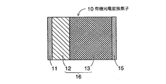
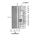
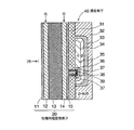
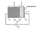
- FIG. 1 is a cross-sectional view showing a first configuration example of an organic photoelectric conversion element according to the present invention.
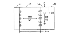
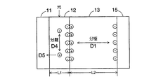
- FIG. 2 is a schematic diagram showing the operating principle of the first configuration example shown in FIG.
- the organic photoelectric conversion element 10 shown in FIG. 1 has a structure including an organic layer 16 between a first electrode 11 and a second electrode 15. 1A and 1B are different in the configuration of the organic layer 16. 1A is an example of a structure in which the charge separation layer 14 is in contact with the second electrode 15, and FIG. 1B is an example of a structure in which the charge separation layer 14 is in contact with the first electrode 11.
- the first electrode 11 and the second electrode 15 correspond to “a pair of electrodes” and are configured to have a difference in work function. Specifically, the electrodes are formed of different materials, or when they are formed of the same material, a bias voltage is applied to one or both electrodes. It is assumed that the work function of the first electrode 11 is larger than the work function of the second electrode 15. Examples of substances applicable to the configurations of the first electrode 11 and the second electrode 15 are shown in the following Table 1 together with the work function.
- the substances forming the first electrode 11 and the second electrode 15 are set so that the work function difference is in the range from 0.1 [eV] to 3 [eV] including the substances shown in Table 1 above. It is desirable to do. This is because when the work function difference is less than 0.1 [eV] or more than 3 [eV], the charges separated by the charge separation layer 14 are difficult to move to the second electrode 15.
- the organic layer 16 is composed of the adjacent insulating polarization layer 13 and the charge separation layer 14 in FIG. 2A, and is composed of the adjacent insulation polarization layer 13 and the charge separation layer 12 in FIG. 2B. Since the insulating polarization layer 13 and the charge separation layer 14 are organic layers as a whole, they may be integrally formed, or may be joined after the insulation polarization layer 13 and the charge separation layer 14 are formed separately. The same is true for the relationship between the insulating polarization layer 13 and the charge separation layer 12 with respect to the integral formation and bonding.
- the insulating polarization layer 13 has a function of insulating and polarizing the electrode (the first electrode 11 or the second electrode 15) and the charge separation layer.
- the film thickness L2 of the insulating polarization layer 13 shown in FIG. 2A is formed thicker than the film thickness L3 of the charge separation layer 14 (ie, L2> L3).
- the thickness L2 of the insulating polarization layer 13 shown in FIG. 2B is formed thicker than the thickness L1 of the charge separation layer 12 (ie, L2> L1). Specifically, it is formed with a thickness of 100 [nm] to 1000 [nm], but preferably with a thickness of 100 [nm] to 300 [nm].
- the thickness of the insulating polarization layer 13 In order to facilitate polarization, it is desirable to increase the thickness of the insulating polarization layer 13 while facilitating polarization. On the other hand, if it is too thick, the electric capacity decreases and the polarization decreases and the transient current decreases. It is because it ends up.
- the insulating polarization layer 13 can be formed of any material.
- PVDF polyvinylidene difluoride
- PTFE polytetrafluoroethylene
- ETFE tetrafluoroethylene / ethylene copolymer
- FEP tetrafluoroethylene -Hexafluoropropylene copolymer
- PFA polychloro-trifluoroethylene
- PCTFE chlorotrifluoroethylene-ethylene copolymer
- ECTFE chlorotrifluoroethylene-ethylene copolymer
- the charge separation layer 14 has a function of separating charges (electrons and holes) by receiving light.
- the charge separation layer 14 is formed with a thickness of 1 [nm] to 50 [nm] (preferably 1 [nm] to 20 [nm], or 10 [nm] to 30 [nm]). Is desirable. This is because the range from 1 [nm] to 20 [nm] is better as the thickness is reduced in order to maintain the internal quantum efficiency high and allow the electrode to absorb the separated charges efficiently. On the other hand, if the thickness is too thin, the separable charge is reduced and the generated transient current is reduced.
- the range from 10 [nm] to 30 [nm] is suitable for securing both a large amount of current and high quantum efficiency. That is, when the thickness of the charge separation layer 14 is increased, the amount of current and the quantum efficiency once increase, but when it exceeds 30 [nm], the quantum efficiency deteriorates.
- the charge separation layer 14 is formed of an appropriate substance (whether or not it is a semiconductor) in accordance with the wavelength of light received when the charge is separated. In other words, any material can be used as long as electrons or holes move to the electrode in contact with the charge separation layer when the light is separated by receiving light. It does not matter whether the mobility of electrons or holes is high or low.
- a donor or acceptor having an absorption band in the specific wavelength range a charge transfer complex having a charge transfer absorption band in a specific wavelength range (an intermolecular compound of a donor and an acceptor) Or a mixture of its donor and acceptor.
- charge separation occurs, and it may be formed using a donor or acceptor that excites an absorption band including a charge transfer absorption band.
- a donor or acceptor that excites an absorption band including a charge transfer absorption band.
- the specific wavelength region is a visible light wavelength region, it is formed of a charge transfer complex having a charge transfer absorption band in the visible light wavelength region, or a mixture of its donor and acceptor.
- the specific wavelength region is an ultraviolet light wavelength region, it is formed of a donor or an acceptor having an absorption band in the ultraviolet light wavelength region, or a mixture of the donor and the acceptor.
- phthalocyanine represented by the chemical formula (Chemical Formula 2) and a fullerene compound are applicable.
- H 2 , TiO, VO, Mn, Fe, Co, Zn, Sn, Pb, Li, or the like can be applied to M coordinated at the center of phthalocyanine.
- fullerene compounds include fullerene C 70 , fullerene C 76 , fullerene C 78 , fullerene C 80 , fullerene C 82 , fullerene C 84 , fullerene C 90 , fullerene C 96 , fullerene C 240 , fullerene C 540 , mixed fullerene, fullerene nanotubes and the like are applicable.
- the fullerene compound described above may include a fullerene derivative to which a substituent is added. Any group can be applied as the substituent. For example, halogen atom, alkyl group, alkenyl group, alkynyl group, aryl group, heterocyclic group, cyano group, hydroxyl group, nitro group, carboxyl group, alkoxy group, aryloxy group, silyloxy group, heterocyclic oxy group, acyloxy group , Carbamoyloxy group, alkoxycarbonyloxy group, aryloxycarbonyloxy group, amino group, ammonio group, acylamino group, aminocarbonylamino group, alkoxycarbonylamino group, aryloxycarbonylamino group, sulfamoylamino group, alkyl and aryl Sulfonylamino group, mercapto group, alkylthio group, arylthio group, heterocyclic thio group, s
- the single component substance include cyclic thiazyl radical (BDTDA) represented by the chemical formula (Chemical Formula 4), N-ethylphenazyl, and the like.
- the specific wavelength region is a wavelength region of infrared light (preferably near infrared light)
- a charge transfer complex having a charge transfer absorption band in infrared light (or near infrared light) or a donor thereof And a mixture of acceptors.
- Any combination of donor and acceptor can be used as long as the above conditions are satisfied.
- a combination of tetrathiafulvalene (TTF) on the donor side shown in (A) of the chemical formula (Chemical Formula 5) and chloranil (CA) on the acceptor side shown in (B) is applicable.
- FIG. 2A corresponds to the structure of FIG. 1A
- FIG. 2B corresponds to the structure of FIG. 2A and 2B are merely reversed in the left-right direction in the drawing, and therefore the structure of FIG. 2A will be described as an example.
- the insulating polarization layer 13 has a thickness of 100 [nm] to 1000 [nm], a hole indicated by plus (+) and an electron indicated by minus ( ⁇ ) are largely polarized as indicated by an arrow D1.
- charge separation layer 14 receives light, charge separation is performed by energy excitation, and holes and electrons are separated as indicated by an arrow D2. Even if the separated holes try to move to the first electrode 11 beyond the insulating polarization layer 13, they cannot move because of the large thickness. On the other hand, the separated electrons are easily moved and absorbed by the adjacent second electrode 15 as indicated by the arrow D3. Since charge separation proceeds in a short time, many electrons flow from the second electrode 15 in a short time, resulting in a transient current. The above operation is the same even if pinholes exist in the charge separation layer 14.
- the charge separation layer 14 directly receives light
- the charge separation layer 12 directly receives light, but may receive light indirectly. That is, in the case where light is received from the left and right sides in FIG. 2, the second electrode 15 or the first electrode 11 and the insulating polarization layer 13 may be formed of a transparent material in FIG. In FIG. 2B, the first electrode 11 or the insulating polarization layer 13 and the second electrode 15 may be formed of a transparent material. Furthermore, when the electrodes and the insulating polarization layer are formed of an opaque material, they may be formed with a thickness that allows light to reach the charge separation layer 14. These materials and thicknesses can be similarly applied to FIGS. 3 and 4 described later.
- the first electrode 11 and the second electrode 15 are formed of materials having different work functions, respectively, and the charge separation layer (the charge separation layer 14 in FIG. 1A and the charge separation layer 14 in FIG. 1B) is formed.
- the charge separation layer 12) and the insulating polarization layer 13 are adjacent to each other (see FIG. 1). According to this configuration, since the insulating polarization layer 13 is interposed between the one electrode and the charge separation layer, even if a pinhole is generated in the manufacturing process of the organic photoelectric conversion element 10, generation of dark current is minimized. It can be suppressed. In addition, polarization of the insulating polarization layer 13 promotes charge separation in the charge separation layer.
- the charge absorbed by the electrode immediately moves to the other electrode due to the difference in work function between the electrodes, so that the responsiveness that current is output after the charge separation layer receives light is improved compared to the conventional case. be able to. Since charge separation proceeds in a short time, a transient current with high efficiency, high speed, and high SN ratio can be obtained. Further, as will be described later, an AC signal can be obtained by irradiating the charge separation layer 14 with chopped light (that is, intermittent pulse waves) (see FIG. 9).
- the first electrode 11 and the second electrode 15 are formed of different materials (see Table 1) so that the work function is different (see Table 1), or one or both electrodes are bias voltage. Was applied. According to this configuration, it is possible to manufacture an organic photoelectric conversion element suitable for the material cost, circuit configuration, and the like.
- the first electrode 11 and the second electrode 15 have a work function difference in a range from 0.1 [eV] to 3 [eV]. According to this configuration, since the charges separated by the charge separation layer are easily absorbed by the adjacent electrodes, a large transient current can be generated quickly.
- the insulating polarization layer 13 was formed thicker than the charge separation layers 12 and 14 (see FIGS. 1 and 2). According to this configuration, since the movement of both holes and electrons is inhibited by the insulating polarization layer 13, the generation of dark current can be more reliably suppressed.
- the charge separation layer 14 shown in FIG. 1A or the charge separation layer 12 shown in FIG. 1B both has a wavelength of 1 [nm] to 50 [nm] (preferably 1 [nm] ] To 20 [nm], or 10 [nm] to 30 [nm].
- a wavelength of 1 [nm] to 50 [nm] preferably 1 [nm] ] To 20 [nm], or 10 [nm] to 30 [nm].
- the insulating polarization layer 13 was formed with a thickness from 100 [nm] to 1000 [nm] (preferably from 100 [nm] to 300 [nm]). According to this configuration, by forming the insulating polarization layer 13 with an appropriate thickness, it is possible to inhibit the movement of both holes and electric charges and reliably suppress the generation of dark current.
- the substance forming the charge separation layers 12 and 14 is made different depending on the wavelength range of the received light.
- the light absorption wavelength can be controlled by appropriately selecting a substance to be formed, and light-current conversion can be realized in a wide range of visible, ultraviolet, and infrared. Even in such a wide wavelength range of light, more charges can be separated.
- the charge separation layers 12 and 14 when receiving light in a specific wavelength range have a donor or acceptor having an absorption band in the specific wavelength range, and a charge transfer absorption band in the specific wavelength range
- the structure is formed of either a charge transfer complex composed of an intermolecular compound of a donor and an acceptor or a mixture of a donor and an acceptor. According to this configuration, more charges can be separated by receiving light in a specific wavelength range.
- the charge separation layers 12 and 14 are such that the specific wavelength range is one or more of the visible wavelength range, the ultraviolet wavelength range, and the infrared wavelength range. It was set as the structure formed by. According to this configuration, the charge separation layers 12 and 14 that have received one or more of visible light, ultraviolet light, and infrared light can separate more charges.
- the second embodiment is an organic photoelectric conversion element having a symmetric structure, and will be described with reference to FIGS.
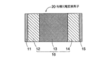
- FIG. 3 is a sectional view showing a second configuration example of the organic photoelectric conversion element according to the present invention.
- FIG. 4 is a schematic diagram showing the operation principle of the second configuration example shown in FIG.
- the second embodiment will be described with respect to differences from the first embodiment. Therefore, the same elements as those used in Embodiment 1 are denoted by the same reference numerals, and description thereof is omitted.
- the organic layer 16 in FIG. 1 is a combination of one charge separation layer (12 or 14) and one insulating polarization layer 13, whereas the organic layer 16 in FIG. 14 and one insulating polarization layer 13 are different.
- the insulating polarization layer 13 is disposed at the center, the charge separation layers 12 and 14 are disposed on both sides of the insulation polarization layer 13, and the first electrode 11 and the second electrode 15 are disposed on the outermost side.
- the operation principle of the organic photoelectric conversion element 20 configured as described above will be described with reference to FIG. Since the insulating polarization layer 13 has a thickness of 100 [nm] to 1000 [nm] as described above, a hole indicated by plus (+) and an electron indicated by minus ( ⁇ ) are large as indicated by an arrow D1. Polarize.
- the “symmetric structure” means the symmetry of the element to the last, and includes the case where the charge separation layer 12 and the charge separation layer 14 have different thicknesses (that is, L1 ⁇ L3).
- the organic layer 16 has a structure having two charge separation layers 12 and 14 and one insulating polarization layer 13 (see FIG. 3). According to this configuration, since electric charge flows from both the first electrode 11 and the second electrode 15, a large transient current can be generated as compared with the organic photoelectric conversion element 10. Since the others are the same as those in the first embodiment, the same operational effects as those in the first embodiment can be obtained.
- the third embodiment is an image pickup device partially including the organic photoelectric conversion device 10 shown in FIG. 1 and will be described with reference to FIG.
- FIG. 5 is a cross-sectional view illustrating a configuration example of the imaging element.
- the third embodiment will be described with respect to differences from the first embodiment. Therefore, the same elements as those used in Embodiment 1 are denoted by the same reference numerals, and description thereof is omitted.
- an image or video is simply referred to as “image or the like”.
- the image pickup device 30 shown in FIG. 5 partially includes the organic photoelectric conversion device 10 shown in FIG. 1 and receives signals (particularly visible light) such as an image for one pixel (a so-called image signal). ) Can be output. That is, the image pickup device 30 is based on the p-type silicon substrate 32, the organic photoelectric conversion device 10, the insulating films 31 and 37, the n-type impurity regions 33 and 35, the p-type impurity regions 34 and 36, the n + -type impurity region 38, and the connection. The structure has a portion 39 and the like. Among these, the n + -type impurity region 38 is a region where the impurity concentration is higher than that of other semiconductor regions.
- the imaging element 30 is joined to the second electrode 15 side of the organic photoelectric conversion element 10 with a transparent insulating film 31 interposed therebetween and a p-type silicon substrate 32 bonded thereto.
- the p-type silicon substrate 32 includes an n + type impurity region 38, a p-type impurity region 36, an n-type impurity region 35, a p-type impurity region 34, and an n-type impurity region 33 in order from the insulating film 31 side to the right side of the drawing. Is formed.
- a connection part 39 connected to the second electrode 15 and an insulating film 37 surrounding the connection part 39 and in contact with the peripheral wall of the insulating film 31 are formed. Yes.
- the connection portion 39 connects the second electrode 15 and the n + -type impurity region 38 so as to be conductive.
- the boundary surface between the n-type impurity region 35 and the p-type impurity region 34 is a pn junction surface.
- the pn junction surface is defined as a distance from a boundary surface between the insulating film 31 and the n-type impurity region 35 (hereinafter simply referred to as “reference surface”) as light in a first target wavelength region (for example, blue of visible light). Is a length that absorbs (for example, about 0.2 [ ⁇ m]).
- the n-type impurity region 35 and the p-type impurity region 34 serve as a first photodiode that absorbs light in the first target wavelength region and accumulates charges corresponding thereto. The charge generated in the first photodiode is accumulated in the n-type impurity region 35.
- the boundary surface between the n-type impurity region 33 and the p-type silicon substrate 32 is also a pn junction surface.
- the pn junction surface has a distance (for example, about 2 [ ⁇ m]) that absorbs light in the second target wavelength region (for example, red of visible light) from the reference surface.
- the n-type impurity region 33 and the p-type silicon substrate 32 become a second photodiode that absorbs light in the second target wavelength region and accumulates charges corresponding thereto. The charge generated in the second photodiode is accumulated in the n-type impurity region 33.
- the n + type impurity region 38 is connected to the second electrode 15 through the connection portion 39. Therefore, the charge that is received by the light and absorbed by the second electrode 15 from the charge separation layer 14 is accumulated in the n + -type impurity region 38 through the connection portion 39.
- the n + -type impurity region 38 corresponds to a “charge storage portion” in that charges are stored.
- the charge separation layer 14 may have a structure that directly receives light as shown in the figure. When the first electrode 11 and the insulating polarization layer 13 are formed of a transparent material, the charge separation layer 14 starts from the first electrode 11 side (the left side in the drawing). A structure that receives light indirectly may be used.
- the charge accumulated in the n-type impurity region 33 is converted into a signal corresponding to the amount of charge by a MOS circuit formed of an n-channel MOS transistor formed in the p-type silicon substrate 32 and output.
- the charge accumulated in n-type impurity region 35 is converted into a signal corresponding to the amount of charge by a MOS circuit formed of an n-channel MOS transistor formed in p-type impurity region 34 and output.
- the charge accumulated in the n + type impurity region 38 is converted into a signal corresponding to the amount of charge by a MOS circuit formed of an n channel MOS transistor formed in the p type impurity region 36 and output.
- each of the above MOS circuits is general, the illustration is omitted, and a signal can be output to the outside by a wiring (not shown). It is desirable to provide an extraction electrode in the n-type impurity region 33 and the n-type impurity region 35. When a predetermined reset potential is applied to the extraction electrode, each region is depleted, so that the capacitance of each pn junction becomes an extremely small value. Therefore, the capacity generated at each joint surface can be extremely reduced.
- One or more of the second electrode 15, the n + -type impurity region 38, the n-type impurity region 35, and the n-type impurity region 33 are connected to a signal output circuit (not shown), and a signal corresponding to the absorbed or accumulated charge Is read.
- the signal output circuit is formed of a CMOS type or a CCD type, but the CMOS type is preferable from the viewpoint of power consumption, reading speed, and the like. It is desirable that the external bias voltage applied to the charge separation layer 14 is also equal to or lower than the drive voltage in order to reduce power consumption in accordance with the drive voltage of the signal output circuit (for example, about 3 [V]).
- the image pickup device 30 is formed on the organic photoelectric conversion device 10 and the semiconductor substrate, reads a current corresponding to the electric charge generated in the one or more organic photoelectric conversion devices 10, and outputs a signal to the outside.
- a CMOS or CCD type signal output unit see FIG. 5.
- the semiconductor substrate has an n + -type impurity region 38 (charge storage portion) that receives light and stores the charges separated by the charge separation layers 12 and 14 of the organic photoelectric conversion element 10 ( (See FIG. 5).
- the charge storage unit is a part that has a power storage function or a charging function. If the charge storage portion is formed large, a large capacity current can be generated after the storage.
- Embodiment 4 is an image pickup device that partially includes the organic photoelectric conversion device 20 shown in FIG. 3, and will be described with reference to FIG.
- FIG. 6 is a cross-sectional view illustrating a configuration example of the imaging element.
- the fourth embodiment will be described with respect to differences from the third embodiment. Therefore, the same elements as those used in the third embodiment are denoted by the same reference numerals and description thereof is omitted.
- the imaging device 40 shown in FIG. 6 includes the organic photoelectric conversion device 20 shown in FIG. 3 in part, and is configured to receive visible light and output it as a signal for one pixel (one pixel).
- the imaging element 40 is based on the p-type silicon substrate 32, and includes the organic photoelectric conversion element 20, the insulating films 31 and 37, the n-type impurity regions 33 and 35, the p-type impurity regions 34 and 36, the n + -type impurity region 38, and the connection.
- the structure has a portion 39 and the like. That is, compared with Embodiment 3, the point which used the organic photoelectric conversion element 20 instead of the organic photoelectric conversion element 10 differs, and the other point is the same. Therefore, except for the function and effect inherent to the organic photoelectric conversion element 20, the same function and effect as those of the third and second embodiments can be obtained.
- the imaging element 40 shown in FIG. 6 includes one organic photoelectric conversion element 20 and receives light (particularly visible light) and outputs a signal such as an image for one pixel.
- a signal such as an image for one pixel.
- an imaging device 40 having other configurations 1 to 4 as described below can be manufactured. Note that a color filter, a prism, or the like is used for color selection from the three primary colors of light.
- one organic photoelectric conversion element 20 and two photodiodes are formed on the p-type silicon substrate 32.
- the charge separation layer 12 (or charge separation layer 14) of one organic photoelectric conversion element 20 receives light in a wavelength region of one of the three primary colors of light and separates the charges.
- the two photodiodes receive light in a wavelength region of a color corresponding to each photodiode for the remaining two colors among the three primary colors of light and separate charges.
- Two organic photoelectric conversion elements 20 and one photodiode are formed on the p-type silicon substrate 32.
- the charge separation layer 12 (or the charge separation layer 14) of the two organic photoelectric conversion elements 20 receives light in a wavelength region of a color corresponding to two of the three primary colors of light and separates the charges.
- One photodiode receives light in the wavelength region of the remaining one color among the three primary colors of light and separates charges.
- Three organic photoelectric conversion elements 20 are formed on the surface side of the p-type silicon substrate 32.
- the three organic photoelectric conversion elements 20 receive the light in the wavelength range of the color corresponding to each of the three primary colors of light and separate the charges.
- the charge separation layers 12 and 14 of the organic photoelectric conversion element 20 are formed of a material in which one or both layers receive light in a wavelength region of ultraviolet or infrared (preferably near infrared) and separate charges.
- a charge separation layer 12 is formed in a vacuum of about 4 ⁇ 10 ⁇ 4 [Pa]. Formed.
- the charge separation layer 12 is a region where organic donors and acceptors are mixed, and includes Zn-phthalocyanine (hereinafter simply expressed as “ZnPc”) represented by the following chemical formula (Formula 6), and a chemical formula (Formula 3).
- ZnPc Zn-phthalocyanine
- the top surface of the charge separation layer 12 was spin-coated with an 8% by weight solution of polyvinylidene difluoride (hereinafter simply referred to as “PVDF”) in dimethylformamide. It was confirmed that the thickness of the insulating polarization layer 13 was 200 [nm]. Further, a second electrode 15 made of aluminum (hereinafter simply referred to as “Al”) was deposited on the upper surface of the insulating polarization layer 13 so as to have a thickness of 60 [nm]. The effective area of the second electrode 15 was 0.02 [cm 2 ] (the same applies to Examples 2 to 14 below).
- Example 2 The first electrode 11 made of ITO was heated to about 100 ° C., and an 8% weight solution of PVDF in dimethylformamide was spin coated as the insulating polarization layer 13. The spin coating was adjusted so that the thickness of the insulating polarization layer 13 was 200 [nm].
- the charge separation layer 14 formed on the upper surface of the insulating polarization layer 13 is a coexisting layer of a donor and an acceptor, and in a vacuum of about 4 ⁇ 10 ⁇ 4 [Pa], ZnPc represented by the above chemical formula (Chemical Formula 6) and a chemical formula ( A co-deposited film having a fullerene C 60 ratio of 1: 1 shown in Chemical Formula 3) was deposited at a rate of 1 [ ⁇ / sec] to a thickness of 50 [nm]. Further, an Al second electrode 15 was deposited on the upper surface of the charge separation layer 14 so as to have a thickness of 60 [nm].
- Example 3 A charge separation layer 12 was formed on the top surface of the first electrode 11 made of ITO in a vacuum of about 4 ⁇ 10 ⁇ 4 [Pa].
- the charge separation layer 12 is a donor, and a deposited film of ZnPc represented by the above chemical formula (Chemical Formula 6) was deposited at a rate of 1 [ ⁇ / sec] to a thickness of 50 [nm].
- the upper surface of the charge separation layer 12 was spin-coated with a 8% by weight PVDF dimethylformamide solution. The spin coating was adjusted so that the thickness of the insulating polarization layer 13 was 200 [nm]. Further, an Al second electrode 15 was deposited on the upper surface of the insulating polarization layer 13 so as to have a thickness of 50 [nm].
- Example 4 The first electrode 11 made of ITO was heated to about 100 ° C., and an 8% weight solution of PVDF in dimethylformamide was spin coated as the insulating polarization layer 13. The spin coating was adjusted so that the thickness of the insulating polarization layer 13 was 200 [nm].
- the charge separation layer 14 formed on the upper surface of the insulating polarization layer 13 is a donor.
- a deposited film made of ZnPc represented by the above chemical formula (Chemical formula 6) is 1 [ ⁇ /
- the film was deposited at a rate of sec] to a thickness of 50 [nm].
- an Al second electrode 15 was deposited on the upper surface of the charge separation layer 14 so as to have a thickness of 60 [nm].
- Example 5 A charge separation layer 12 was formed on the top surface of the first electrode 11 made of ITO in a vacuum of about 4 ⁇ 10 ⁇ 4 [Pa].
- the charge separation layer 12 is an acceptor, and a C60 vapor deposition film represented by the above chemical formula (Chemical Formula 6) was deposited at a rate of 1 [ ⁇ / sec] to a thickness of 50 [nm].
- the upper surface of the charge separation layer 12 was spin-coated with a 8% by weight PVDF dimethylformamide solution. The spin coating was adjusted so that the thickness of the insulating polarization layer 13 was 200 [nm]. Further, an Al second electrode 15 was deposited on the upper surface of the insulating polarization layer 13 so as to have a thickness of 50 [nm].
- Example 6 The first electrode 11 made of ITO was heated to about 100 ° C., and an 8% weight solution of PVDF in dimethylformamide was spin coated as the insulating polarization layer 13. The spin coating was adjusted so that the thickness of the insulating polarization layer 13 was 200 [nm].
- the charge separation layer 14 formed on the upper surface of the insulating polarization layer 13 is an acceptor, and in a vacuum of about 4 ⁇ 10 ⁇ 4 [Pa], a deposited film made of C60 represented by the above chemical formula (Chemical Formula 6) is 1 [ ⁇ / The film was deposited at a rate of sec] to a thickness of 50 [nm]. Further, an Al second electrode 15 was deposited on the upper surface of the charge separation layer 14 so as to have a thickness of 60 [nm].
- Example 7 The first electrode 11 made of ITO was heated to about 100 ° C., and an 8% weight solution of PVDF in dimethylformamide was spin coated as the insulating polarization layer 13. The spin coating was adjusted so that the thickness of the insulating polarization layer 13 was 200 [nm].
- the charge separation layer 14 formed on the upper surface of the insulating polarization layer 13 is a layer in which a donor and an acceptor are mixed.
- ZnPc represented by the above chemical formula (Formula 6) and a chemical formula A co-evaporated film having a fullerene C 60 ratio of 1: 1 shown in (Chemical Formula 3) was deposited at a rate of 1 [ ⁇ / sec] to a thickness of 50 [nm]. Further, a second electrode 15 made of silver (Ag) was deposited on the upper surface of the charge separation layer 14 so as to have a thickness of 60 [nm].
- Example 8 The first electrode 11 made of ITO was heated to about 100 ° C., and an 8% weight solution of PVDF in dimethylformamide was spin coated as the insulating polarization layer 13. The spin coating was adjusted so that the thickness of the insulating polarization layer 13 was 200 [nm].
- the charge separation layer 14 formed on the upper surface of the insulating polarization layer 13 is a layer in which a donor and an acceptor are mixed.
- ZnPc represented by the above chemical formula (Formula 6) and a chemical formula A co-evaporated film having a fullerene C 60 ratio of 1: 1 shown in (Chemical Formula 3) was deposited at a rate of 1 [ ⁇ / sec] to a thickness of 50 [nm]. Further, a second electrode 15 made of copper (Cu) was deposited on the upper surface of the charge separation layer 14 so as to have a thickness of 60 [nm].
- Example 9 The first electrode 11 made of ITO was heated to about 100 ° C., and an 8% weight solution of PVDF in dimethylformamide was spin coated as the insulating polarization layer 13. The spin coating was adjusted so that the thickness of the insulating polarization layer 13 was 200 [nm].
- the charge separation layer 14 formed on the upper surface of the insulating polarization layer 13 is a layer in which a donor and an acceptor are mixed.
- a bis (4 A vapor-deposited film made of -dimethylaminodithiobenzyl) nickel (II) was deposited at a rate of 0.5 [ ⁇ / sec] to a thickness of 50 [nm].
- a second electrode 15 made of silver (Ag) was deposited on the upper surface of the charge separation layer 14 so as to have a thickness of 50 [nm].
- the bis (4-dimethylaminodithiobenzyl) nickel (II) is indicated as “BDN” in the column of Example 9 in FIG. 7A described later.
- Example 10 A charge separation layer 12 was formed on the top surface of the first electrode 11 made of ITO in a vacuum of about 4 ⁇ 10 ⁇ 4 [Pa].
- the charge separation layer 12 is a layer in which a donor and an acceptor are mixed, and is a co-deposited film in which ZnPc represented by the chemical formula (Chemical Formula 6) and fullerene C 60 represented by the chemical formula (Chemical Formula 3) are 1: 1.
- the film was deposited at a rate of 1 [ ⁇ / sec] to a thickness of 50 [nm].
- the upper surface of the charge separation layer 12 was spin-coated with a 8% by weight PVDF dimethylformamide solution. The spin coating was adjusted so that the thickness of the insulating polarization layer 13 was 200 [nm].
- the charge separation layer 14 formed on the upper surface of the insulating polarization layer 13 was deposited in the same manner as the charge separation layer 12 to a thickness of 50 [nm]. Further, an Al second electrode 15 was deposited on the upper surface of the charge separation layer 14 so as to have a thickness of 60 [nm].
- Example 11 A charge separation layer 12 was formed on the top surface of the first electrode 11 made of ITO in a vacuum of about 4 ⁇ 10 ⁇ 4 [Pa].
- the charge separation layer 12 is a layer in which a donor and an acceptor are mixed, and is a co-deposited film in which ZnPc represented by the chemical formula (Chemical Formula 6) and fullerene C 60 represented by the chemical formula (Chemical Formula 3) are 1: 1.
- the film was deposited at a rate of 1 [ ⁇ / sec] to a thickness of 100 [nm].
- the upper surface of the charge separation layer 12 was spin-coated with a 8% by weight PVDF dimethylformamide solution. The spin coating was adjusted so that the thickness of the insulating polarization layer 13 was 200 [nm].
- the charge separation layer 14 formed on the upper surface of the insulating polarization layer 13 was deposited in the same manner as the charge separation layer 12 to a thickness of 100 [nm]. Further, an Al second electrode 15 was deposited on the upper surface of the charge separation layer 14 so as to have a thickness of 60 [nm].
- Example 12 A charge separation layer 12 was formed on the top surface of the first electrode 11 made of ITO in a vacuum of about 4 ⁇ 10 ⁇ 4 [Pa].
- the charge separation layer 12 is a layer in which a donor and an acceptor are mixed, and is a co-deposited film in which ZnPc represented by the chemical formula (Chemical Formula 6) and fullerene C 60 represented by the chemical formula (Chemical Formula 3) are 1: 1.
- the film was deposited at a rate of 1 [ ⁇ / sec] to a thickness of 25 [nm].
- the upper surface of the charge separation layer 12 was spin-coated with a 8% by weight PVDF dimethylformamide solution. The spin coating was adjusted so that the thickness of the insulating polarization layer 13 was 200 [nm].
- the charge separation layer 14 formed on the upper surface of the insulating polarization layer 13 was deposited in the same manner as the charge separation layer 12 to a thickness of 25 [nm]. Further, an Al second electrode 15 was deposited on the upper surface of the charge separation layer 14 so as to have a thickness of 60 [nm].
- Example 13 A charge separation layer 12 was formed on the top surface of the first electrode 11 made of ITO in a vacuum of about 4 ⁇ 10 ⁇ 4 [Pa].
- the charge separation layer 12 is a layer in which a donor and an acceptor are mixed, and is a co-deposited film in which ZnPc represented by the chemical formula (Chemical Formula 6) and fullerene C 60 represented by the chemical formula (Chemical Formula 3) are 1: 1.
- the film was deposited at a rate of 1 [ ⁇ / sec] to a thickness of 50 [nm].
- the upper surface of the charge separation layer 12 was spin-coated with a 8% by weight PVDF dimethylformamide solution. The spin coating was adjusted so that the thickness of the insulating polarization layer 13 was 100 [nm].
- the charge separation layer 14 formed on the upper surface of the insulating polarization layer 13 was deposited in the same manner as the charge separation layer 12 to a thickness of 50 [nm]. Further, an Al second electrode 15 was deposited on the upper surface of the charge separation layer 14 so as to have a thickness of 60 [nm].
- Example 14 A charge separation layer 12 was formed on the top surface of the first electrode 11 made of ITO in a vacuum of about 4 ⁇ 10 ⁇ 4 [Pa].
- the charge separation layer 12 is a layer in which a donor and an acceptor are mixed, and is a co-deposited film in which ZnPc represented by the chemical formula (Chemical Formula 6) and fullerene C 60 represented by the chemical formula (Chemical Formula 3) are 1: 1.
- the film was deposited at a rate of 1 [ ⁇ / sec] to a thickness of 50 [nm].
- the upper surface of the charge separation layer 12 was spin-coated with a 8% by weight PVDF dimethylformamide solution. The spin coating was adjusted so that the thickness of the insulating polarization layer 13 was 400 [nm].
- the charge separation layer 14 formed on the upper surface of the insulating polarization layer 13 was deposited in the same manner as the charge separation layer 12 to a thickness of 50 [nm]. Further, an Al second electrode 15 was deposited on the upper surface of the charge separation layer 14 so as to have a thickness of 60 [nm].
- Example 15 When a bias circuit is configured using the organic photoelectric conversion elements 10 shown in Examples 1 to 9, the result is as shown in FIG.
- the first electrode 11 is formed of ITO
- the insulating polarization layer 13 is formed of PVDF
- the charge separation layer 14 is formed of Li-phthalocyanine represented by the following chemical formula (Formula 8) (hereinafter simply referred to as “LiPc”).
- the second electrode 15 is formed of Al.
- a CW laser having a wavelength of 532 [nm] and an intensity of 4 [mW / cm 2 ] is used as the light applied to the charge separation layers 12 and 14.
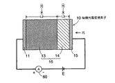
- an ammeter 60 and a battery E are connected between the first electrode 11 and the second electrode 15.
- the ammeter 60 is a measuring instrument for measuring bias characteristics.
- the battery E is a power source for applying a bias to the organic photoelectric conversion element 10.
- the positive terminal of the battery E is connected to the first electrode 11 side, and the negative terminal is connected to the second electrode 15 side.
- Each characteristic when the voltage of the battery E is ⁇ 5 [V], 0 [V], +5 [V] is shown in FIG.
- the bias characteristics of FIG. 14 it can be seen that the photocurrent increases as the bias voltage increases in the positive direction.
- a charge separation layer 12 was formed on the top surface of the first electrode 11 made of ITO in a vacuum of about 4 ⁇ 10 ⁇ 4 [Pa].
- the charge separation layer 12 is a layer in which a donor and an acceptor are mixed, and is a co-deposited film in which ZnPc represented by the chemical formula (Chemical Formula 6) and fullerene C 60 represented by the chemical formula (Chemical Formula 3) are 1: 1.
- the film was deposited at a rate of 1 [ ⁇ / sec] to a thickness of 0.2 [nm].
- the upper surface of the charge separation layer 12 was spin-coated with a 8% by weight PVDF dimethylformamide solution.
- the spin coating was adjusted so that the thickness of the insulating polarization layer 13 was 200 [nm].
- the charge separation layer 14 formed on the upper surface of the insulating polarization layer 13 was deposited in the same manner as the charge separation layer 12 to a thickness of 0.2 [nm]. Further, an Al second electrode 15 was deposited on the upper surface of the charge separation layer 14 so as to have a thickness of 60 [nm].
- a charge separation layer 12 was formed on the top surface of the first electrode 11 made of ITO in a vacuum of about 4 ⁇ 10 ⁇ 4 [Pa].
- the charge separation layer 12 is a layer in which a donor and an acceptor are mixed, and is a co-deposited film in which ZnPc represented by the chemical formula (Chemical Formula 6) and fullerene C 60 represented by the chemical formula (Chemical Formula 3) are 1: 1.
- the film was deposited at a rate of 1 [ ⁇ / sec] to a thickness of 50 [nm].
- the upper surface of the charge separation layer 12 was spin-coated with a 8% by weight PVDF dimethylformamide solution.
- the spin coating was adjusted so that the thickness of the insulating polarization layer 13 was 1 [nm].
- the charge separation layer 14 formed on the upper surface of the insulating polarization layer 13 was deposited in the same manner as the charge separation layer 12 to a thickness of 50 [nm]. Further, an Al second electrode 15 was deposited on the upper surface of the charge separation layer 14 so as to have a thickness of 60 [nm].
- a charge separation layer 12 was formed on the top surface of the first electrode 11 made of ITO in a vacuum of about 4 ⁇ 10 ⁇ 4 [Pa].
- the charge separation layer 12 is a layer in which a donor and an acceptor are mixed, and is a co-deposited film in which ZnPc represented by the chemical formula (Chemical Formula 6) and fullerene C 60 represented by the chemical formula (Chemical Formula 3) are 1: 1.
- the film was deposited at a rate of 1 [ ⁇ / sec] to a thickness of 50 [nm].
- the upper surface of the charge separation layer 12 was spin-coated with a 8% by weight PVDF dimethylformamide solution.
- the spin coating was adjusted so that the thickness of the insulating polarization layer 13 was 2000 [nm].
- the charge separation layer 14 formed on the upper surface of the insulating polarization layer 13 was deposited in the same manner as the charge separation layer 12 to a thickness of 50 [nm]. Further, an Al second electrode 15 was deposited on the upper surface of the charge separation layer 14 so as to have a thickness of 60 [nm].
- the first electrode 11 and the second electrode 15 are directly connected by a conducting wire to be in a state under a zero bias voltage. Further, a CW laser having a wavelength of 532 [nm], a frequency of 1000 [Hz], and an intensity of 31.8 [mW / cm 2 ] is used as the light applied to the charge separation layers 12 and 14.
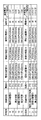
- FIG. 7 shows a transient current value (peak value) generated when the charge separation layers 12 and 14 are irradiated with the CW laser.
- the table in FIG. 7A shows the results of Examples 1 to 9 corresponding to Embodiment 1 (organic photoelectric conversion element 10 having an asymmetric structure).
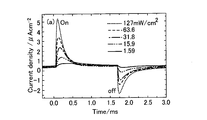
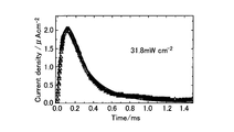
- FIG. 8 shows the change when the intensity is changed without changing the wavelength and frequency of the CW laser.
- FIG. 8 is a graph showing a change with time of current density (Current / density) with respect to presence / absence of laser light (On / Off).
- Current / density current density
- the current density of the transient current increases as the intensity of the CW laser increases. Further, the current density changes in the positive direction when irradiation with the CW laser is started, but the current density changes in the negative direction when irradiation with the CW laser is stopped.
- the transient current (current density) changes as shown in FIG.
- the transient current changes with irradiation / non-irradiation, and the peak value is kept substantially constant.
- FIG. 10 shows changes in the transient current when the frequency and intensity of the CW laser are constant and the wavelength is changed.
- FIG. 10 shows an example of the organic photoelectric conversion elements 10 and 20 using the co-deposited film of ZnPc and fullerene C 60 for the charge separation layers 12 and 14.
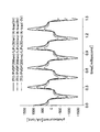
- FIG. 10 is a graph showing changes in absorption spectrum and photocurrent corresponding to a transient current with respect to the wavelength of light. As is clear from FIG. 10, the absorption spectrum becomes maximum near 400 [nm], while the photocurrent becomes maximum near 620 [nm].
- the organic photoelectric conversion elements 10 and 20 using ZnPc for the charge separation layers 12 and 14 exhibit different characteristics. That is, the characteristics change depending on what kind of material is used for the charge separation layers 12 and 14.
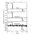
- FIG. 12 shows a change in the transient current when the material for forming the insulating polarization layer 13 is changed with the condition of the irradiated light being constant.
- FIG. 12 is a graph showing the change over time in the current density (Current / density) corresponding to the transient current with respect to the presence or absence of light (On / Off).
- an example formed with PVDF is shown in FIG. 12A
- an example formed with polystyrene is shown in FIG. 12B
- an example formed in a vacuum space is shown in FIG. 12C.
- FIG. 15 shows a circuit diagram for measuring the output characteristics of the organic photoelectric conversion element.
- FIG. 16 is a graph showing the output characteristics of the circuit diagram of FIG.
- a resistor R is connected between the first electrode 11 and the second electrode 15, and a voltmeter 50 is connected to both ends of the resistor R.
- the irradiation direction of the CW laser having a wavelength as near infrared light of 1064 [nm] and a frequency of 1000 [Hz] is indicated by an arrow. What is measured by the voltmeter 50 is a photovoltage corresponding to a transient current.
- FIG. 17 shows a circuit diagram for examining the film thickness dependence of the charge separation layer.
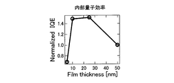
- FIG. 18 is a graph showing the film thickness dependence according to the circuit diagram of FIG. Specifically, FIG. 18A shows a change with time in current density (Current density), and FIG. 18B shows a change in external quantum efficiency (EQE) with respect to the thickness of the charge separation layer.
- FIG. 18C shows the change in internal quantum efficiency (IQE) with respect to the layer thickness.
- IQE internal quantum efficiency
- the organic photoelectric conversion element 10 illustrated in FIG. 1A is applied as an example, and an ammeter 60 is connected between the first electrode 11 and the second electrode 15.
- the organic photoelectric conversion element 10 is configured in the same manner as in the above-described embodiment. That is, the first electrode 11 is formed of ITO, the insulating polarization layer 13 is formed of PVDF, the charge separation layer 14 is formed of a co-deposited film of ZnPc and fullerene C 60, and the second electrode 15 is formed of Al. .
- the thickness L2 of the insulating polarization layer 13 is 200 [nm]. Under this condition, when the film thickness L3 of the charge separation layer 14 is changed by 5, 10, 25, 50 [nm], the characteristics shown in FIG. 18 are obtained.
- the current density (that is, the amount of current) increases as the thickness L3 of the charge separation layer 14 increases.
- the external quantum efficiency increases as the film thickness L3 increases.
- the internal quantum efficiency once increases as the film thickness L3 increases, but 10 to 30 [nm] is maximized. The internal quantum efficiency is low. From this, when the film thickness L3 is increased, the amount of current and the quantum efficiency once increase, but when the thickness exceeds the predetermined thickness, the quantum efficiency deteriorates. Therefore, in order to ensure both a large amount of current and high quantum efficiency, it is desirable to form the film thickness L3 of the charge separation layer 14 at 10 to 30 [nm].
- the organic photoelectric conversion element 10 illustrated in FIG. 1A has been described.
- the organic photoelectric conversion element 10 illustrated in FIG. 1B is applied, the organic photoelectric conversion element illustrated in FIG. Even when 20 is applied, the same characteristics as in FIG. 18 can be obtained.
- the insulating polarization layer 13 is formed with a thickness other than 200 [nm] in the range of 100 [nm] to 1000 [nm], the same characteristics as in FIG. 18 can be obtained.
- Examples 1 to 14 described above ITO was used as the first electrode 11 and Al, Ag, and Cu were used as the second electrode 15.
- Other materials may be used for the first electrode 11 and the second electrode 15 so that the work function varies within a range from 0.1 [eV] to 3 [eV].
- the other substances are not limited to the substances shown in Table 1, for example, and metals other than those in Table 1, metal oxides, compounds of metals and organic substances, and the like are applicable. Even when such other materials are used as electrodes, a transient current equivalent to that of the above-described Examples 1 to 14 occurs.
- the semiconductor substrate includes one organic photoelectric conversion element and two photodiodes,
- the charge separation layer of one of the organic photoelectric conversion elements receives light in a wavelength region of one color among the three primary colors of light, and separates charges.
- the two photodiodes are configured to receive charges in a wavelength region of a color corresponding to each of the photodiodes for the remaining two colors among the three primary colors of light, and to separate charges. Or the imaging device of 12.
- the semiconductor substrate includes two organic photoelectric conversion elements and one photodiode.
- the charge separation layer of the two organic photoelectric conversion elements receives light in a wavelength region of a color corresponding to each semiconductor for two colors among the three primary colors of light, and separates charges.
- 13 The image pickup device according to claim 11, wherein one of the photodiodes is configured to receive charges in a wavelength region of the remaining one color among the three primary colors of the light and separate charges.
- One of the three primary colors of light is received by the photodiode and converted into current, and the two colors are received by the organic photoelectric conversion element 20 and converted into current.
- the generation of dark current is further suppressed as compared with an element configured to convert all three colors into a transient current using a photodiode, so that the color tone can be further improved.
- Aspect 3 Three organic photoelectric conversion elements are formed on the surface side of the semiconductor substrate, The three organic photoelectric conversion elements are configured to receive light in a wavelength region of a color corresponding to each semiconductor for each of the three primary colors of light and to separate charges. Image sensor.
- the organic photoelectric conversion element 20 receives all the three primary colors of light and converts them into current. Compared with an element configured to convert a transient current into three colors using a photodiode, generation of dark current is greatly suppressed, and thus the color tone can be further improved.
- the organic photoelectric conversion element 20 receives ultraviolet light or infrared light and converts it into current. Since dark current is greatly suppressed, detection performance can be improved.
- the organic photoelectric conversion device of the present invention has a function of receiving light and generating a current. According to this function, it can be applied as a light-current conversion element, an alternating current solar cell, a light sensor (including a photodiode), a light intensity sensor, a photoresistor, a phototransistor, a pyroelectric detector, and the like.
- the light-current conversion element converts an infrared pulse in an optical fiber into a current at an extremely high speed.
- the AC solar cell uses a required number of the organic photoelectric conversion elements of the present invention, and outputs an AC current (AC power) by sunlight chopped using natural energy such as hydraulic power or wind power.
- the optical sensor detects light and outputs a current (signal).
- the light intensity sensor detects the intensity of light.
- the electrical resistance of the photoresistor changes depending on the intensity of light.
- the phototransistor has a built-in mechanism for amplifying a current output by receiving light from the organic photoelectric conversion element of the present invention.
- the pyroelectric detector effectively functions as a thermometer in response to heat generated by receiving light.
- First electrode (a pair of electrodes) 12, 14 Charge separation layer 13 Insulating polarization layer 15 Second electrode (a pair of electrodes) 16 Organic layer 30, 40 Image sensor 31, 37 Insulating film 32 p-type silicon substrate (semiconductor substrate) 33, 35 n-type impurity region 34, 36 p-type impurity region 38 n + -type impurity region 39 connection portion
Landscapes
- Physics & Mathematics (AREA)
- Electromagnetism (AREA)
- Light Receiving Elements (AREA)
Abstract
【課題】安価に作製でき、暗電流の発生が極力抑えられ、光を受けて大きくかつ高速の応答性をもつ過渡電流を発生させることができる有機光電変換素子および撮像素子を提供することを目的とする。 【解決手段】第1電極11と第2電極15とからなる一対の電極と、一対の電極間に備えられる有機層16とを有し、光を受けて電流を発生させる有機光電変換素子10において、第1電極11と第2電極15とは仕事関数に差をつけ、有機層16は、光を受けて電荷(電子と正孔)を分離する電荷分離層12,14と、一方の電極と電荷分離層12,14とを絶縁して分極する絶縁分極層13とを隣接させる構造とした。
Description
本発明は、一対の電極(第1電極および第2電極)間に有機層を備え、光を受けて電流を発生させる有機光電変換素子に関する。
従来、実用化されている光検出器としては、無機半導体のpn接合やショットキー接合に負のバイアス電圧を印加して作動させるタイプが知られており、光検出器が光通信やイメージセンサーなどとして広く用いられている。ここでは、無機半導体層に吸収された光子は、電荷分離を経て電流に変換される。このような無機半導体素子に対して、作製の容易さや経済性、構造柔軟性や強い光吸収能のため、有機の光検出器に関する関心が急速に高まりつつある。この作動原理は、基本的には無機半導体を有機物に置き換えて、電流の発生効率を高める。具体的には、ホールおよび電子輸送層を金属電極とpn接合(ドナー-アクセプター接合)を含む光活性層の間に挿入する構造である(以上は例えば特許文献1,2および非特許文献1,2を参照)。
また、赤外光焦電検出器の用途は広く、火災報知機や侵入者探知、イメージセンサーなどに広く利用されている。この作動は、光-フォノン変換とフォノン-電流変換の二つのプロセスからなる。検知器は、無機材料の光焦電素子薄膜が電極に挟まれた構造を持ち、焦電材料の分極方向が電極面に垂直になるように配置されている。光吸収が起こると光焦電素子の温度が上がり、これによって素子の分極率が時間変化することによってパルス電流が生じ、これをプリアンプで増幅してシグナル(電流)として取り出す構造である(以上は例えば特許文献3,4および非特許文献3,4を参照)。
一方、一対の電極間に有機層を備えた有機光電変換素子としては、光電変換膜(有機層)にフラーレン又はフラーレン誘導体を含有する撮像素子に関する技術が開示されている(例えば特許文献5を参照)。また、光導電性有機化合物を含有する層(有機層)の一部または全部に、キナクリドン系色素のような配向分子を用いた有機光電変換素子に関する技術が開示されている(例えば特許文献6を参照)。さらに、電極と有機光電変換層(有機層)との間に、電極から有機光電変換層に向かって電荷が注入されるのを抑制するために金属酸化体で構成されるブロッキング層を備えた光電変換素子に関する技術が開示されている(例えば特許文献7を参照)。
Taichiro Morimune, HirotakeKajii, and Yutaka Ohmori, Photoresponse Properties of a High-Speed OrganicPhotodetector Based on Copper Phthalocyanine Under Red Light Illumination, IEEEPhotonics Technology Letters, 18, 2662-2664 (2006).
P. Peumans, V. Bulovic, and S. R.Forrest, Efficient, high-bandwidth organic multilayer photodetectors, AppliedPhysics Letters, 76, 3855-3857 (2000).
Kazuhiko Hashimoto, TomohiroTsuruta, Koji Nishimura, Katsuya Morinaka, Mariko Kawaguri and NobuyukiYoshiike, Characteristics of Pyroelectric Infrared Array Detector Made ofPbTi03 Ceramics, Jpn. J. Appl. Phys., 36, 3553-3557 (1997).
Andrzej Odon, Voltage Response ofPyroelectric PVDF Detector to Pulse Source of Optical Radiation, MeasurementScience Review, 5, 55-58 (2005).
しかし、シリコンダイオードを用いた光検出器では、システムが複雑で安価に作製することができないという問題点がある。また、無機半導体は一般に高伝導度であるため、暗電流によるノイズが大きいという問題点がある。
また、有機物中の電気伝導は主にホッピング伝導によって生じるため、電子やホールの移動度が小さいという問題点がある。このように移動度が小さければ、電極から20[nm]程度の深さにある有機層における電荷分離しか光伝導に寄与できない。バイアス電圧を加え、有機層の厚さを増すなどして応答度や光電流を高めようとすると、内部量子効率を減少させてしまい、さらには有機物自体が化学的に不安定になり易いという問題点がある。
上記問題点を解消するために、薄膜検出素子を積層する方法も考えられる。ところが、蒸着やスピンコートなどの製法で作製すると半導体にピンホールが発生し易く、ピンホールの存在によって暗電流(あるいは漏れ電流)が発生し易くなるという問題点がある。
本発明はこのような点に鑑みてなしたものであり、安価に作製でき、暗電流の発生が極力抑えられ、光を受けて大きくかつ高速の応答性をもつ過渡電流を発生させることができる有機光電変換素子および撮像素子を提供することを目的とする。
上記課題を解決するためになされた請求項1に記載の発明は、第1電極と第2電極とからなる一対の電極と、前記一対の電極間に備えられる有機層とを有し、光を受けて電流を発生させる有機光電変換素子において、前記第1電極と前記第2電極とは仕事関数に差をつけ、前記有機層は、光を受けて電荷(電子と正孔(ホール))を分離する電荷分離層と、一方の前記電極と前記電荷分離層とを絶縁して分極する絶縁分極層と、を隣接させる構造とすることを特徴とする。
この構成によれば、一方の電極(例えば第1電極)と電荷分離層との間には絶縁分極層が介在され、他方の電極(例えば第2電極)は電荷分離層と接する。一方の電極と電荷分離層との間に絶縁分極層が介在するので、有機光電変換素子の製造過程で仮にピンホールが発生したとしても、暗電流の発生が極力抑えられる。これは、電荷分離層で分離された電荷が一方の電極に移動しようとしても、電荷分離層がホール(正孔)および電子の双方について移動を阻害するからである。また、絶縁分極層に生じる分極は、電荷分離層中の電荷分離を促進し、また電荷分離後、電荷の電極への吸収を促進する。第一電極と第二電極が外部回路によって短絡されている場合は、電荷分離層に接した電極に吸収された電荷は、ふたつの電極間の仕事関数の差によって即座に他方の電極に移動する。薄い電荷分離層を使うことによって有機物の低移動度が問題にならないこと、絶縁分極層が電荷分離と電荷の電極への吸収を助けることにより、電荷分離層が光を受けてから過渡電流が出力される応答性(高い光-電流変換効率および短い光-電流変換時間)を従来よりも高めることができる。
ここで、「仕事関数」は理化学辞典第5版(岩波書店,1998年)にも記載されているように、物質(金属や半導体の結晶等)表面からその外側へ1個の電子を取り出すのに必要な最小のエネルギーを意味する。「電荷分離層」は光を受けて電荷を分離する化合物であれば任意の物質で形成してよく、半導体(p型やn型等の型式を含めて)か否かを問わない。すなわち、光を受けて電荷を分離するにあたって、電子あるいはホールが、電荷分離層が接している電極まで移動する物質であればよい。光を直接的に受ける構成としてもよく、電極および絶縁分極層のうちで一方または双方を透明材料で形成する場合には光を間接的に受ける構成としてもよい。一方、電極および絶縁分極層を不透明材料で形成する場合には、光が電荷分離層に到達可能な厚みで形成すればよい。「絶縁分極層」は誘電体や絶縁体に相当する層であり、電荷分離層における電荷の分離や、分離した電荷が他方の電極に吸収し易くする作用を奏する。一対の電極(第1電極および第2電極)は、直流電源のようにどちらか一方を陽極(プラス極)とし他方を陰極(マイナス極)として用いることもでき、交流電源のように双方ともに極性が変換する電極として用いることもできる。層が「隣接する」とは、面接触や面接合等によってホールや電子が移動可能な形態を意味する。
請求項2に記載の発明は、前記有機層は、二つの前記電荷分離層と、一つの前記絶縁分極層とを有し、前記二つの電荷分離層は、一方の前記電荷分離層を前記第1電極と前記絶縁分極層との間に介在させ、他方の前記電荷分離層を前記第2電極と前記絶縁分極層との間に介在させる構造としたことを特徴とする。請求項2は、電極と絶縁分極層との間にそれぞれ電荷分離層を介在させた点で請求項1と相違する。この構成によれば、中央部に絶縁分極層が配置され、当該絶縁分極層の両側(対向面)に二つの電荷分離層がそれぞれ配置され、一番外側に第1電極と第2電極とがそれぞれ配置される構造となる。すなわち一対の電極から、電子とホールを取り出すことができ、より大きな過渡電流を出力できる。
請求項3に記載の発明は、前記第1電極と前記第2電極とは、仕事関数に差がつくように、異なる物質で形成するか、あるいは一方または双方の電極にバイアス電圧を印加することを特徴とする。この構成によれば、仕事関数に差がつくように第1電極および第2電極を構成すればよい。したがって、物質のコストや回路構成等に見合う適切な有機光電変換素子を製造することができる。
請求項4に記載の発明は、前記第1電極と前記第2電極とは、仕事関数の差が0.1[eV]から3[eV]までの範囲とすることを特徴とする。仕事関数の差が0.1[eV]未満の場合や、3[eV]を超える場合には、活性層(すなわち電荷分離層)からの電荷が電極に移動するのが妨げられ易くなる。この構成によれば、仕事関数の差が0.1[eV]から3[eV]までの範囲となるように第1電極および第2電極を構成するので、電荷分離層で分離された電荷は、当該電荷分離層に隣接する電極に移動し易くなる。したがって、迅速かつ大きな電流を発生させることができる。
請求項5に記載の発明は、前記絶縁分極層は、前記電荷分離層よりも厚く形成することを特徴とする。この構成によれば、電荷分離層で分離された電荷は、厚く形成された絶縁分極層によってホールおよび電子の双方について移動が阻害されるので、暗電流の発生をより確実に抑えることができる。
請求項6に記載の発明は、前記電荷分離層は、1[nm]から50[nm]までの厚さで形成することを特徴とする。好ましくは、1[nm]から20[nm]までの厚さで形成するのが望ましい。光を受けて電荷を分離するには電荷分離層の厚さが薄いのが望ましい反面、薄くなり過ぎると分離可能な電荷が少なくなって出力する電流が小さくなってしまう。また好ましくは、10[nm]から30[nm]までの厚さで形成するのが望ましい。電荷分離層の厚さを増してゆくと、一旦は電流量や量子効率が増えるものの、30[nm]を超えると量子効率が悪化する。大きな電流量および高い量子効率の双方を確保できるのは、10[nm]から30[nm]の範囲である。この構成によれば、適切な厚さで電荷分離層を形成することで、光を受けて電荷を分離し易く、かつ可能な限り大きな電流を発生させることができる。
請求項7に記載の発明は、前記絶縁分極層は、100[nm]から1000[nm]までの厚さで形成することを特徴とする。好ましくは、100[nm]から300[nm]までの厚さで形成するのが望ましい。分極し易くするには絶縁分極層の厚さを厚くするのが望ましい反面、厚くなり過ぎると電気容量が減少し、分極が減少して過渡電流が小さくなってしまう。この構成によれば、適切な厚さで絶縁分極層を形成することで、ホールおよび電子の双方について移動を阻害して、暗電流の発生を確実に抑えることができる。
請求項8に記載の発明は、受ける光の波長域に応じて前記電荷分離層を形成する物質を異ならせることを特徴とする。電荷分離層を形成する物質は、光の波長域に応じて分離できる電荷の量が変化する。この構成によれば、可視光・紫外光・赤外光等のように光の波長域に適した物質で電荷分離層を形成するので、各波長域でより多くの電荷を分離することができる。
請求項9に記載の発明は、特定の波長域にかかる光を受ける場合の前記電荷分離層は、前記特定の波長域に吸収帯をもつドナー(電子供与体)またはアクセプター(受容体)、前記特定の波長域に電荷移動吸収帯をもつドナーとアクセプターとの化合物からなる電荷移動錯体、あるいは前記ドナーと前記アクセプターとの混合物のいずれかで形成することを特徴とする。すなわち電荷分離層は、(α)特定の波長域に吸収帯をもつドナー、(β)特定の波長域に吸収帯をもつアクセプター、(γ)特定の波長域に電荷移動吸収帯をもつドナーとアクセプターとの化合物からなる電荷移動錯体、(δ)上記(α)から(γ)に示すドナーとアクセプターとの混合物、のいずれかで形成する。この構成によれば、特定の波長域に吸収帯をもつ物質で電荷分離層を形成することで、電荷分離層はより多くの電荷を分離することができる。
請求項10に記載の発明は、前記特定の波長域は、可視光の波長域、紫外光の波長域、赤外光の波長域(望ましくは近赤外光の波長域)のうちで一以上の波長域とすることを特徴とする。この構成によれば、可視光、紫外光、赤外光のうちで一以上の光を受けた電荷分離層はより多くの電荷を分離することができる。
請求項11に記載の発明は、半導体基板を有する撮像素子において、前記半導体基板の表面側に形成され、請求項1から10のいずれか一項に記載の一以上の有機光電変換素子と、前記半導体基板に形成され、前記一以上の有機光電変換素子で発生した電荷に応じた電流を読み出して外部に信号を出力するCMOS型又はCCD型の信号出力部と、を有することを特徴とする。この構成によれば、有機光電変換素子(具体的には電荷分離層)で発生した電荷に応じた電流が出力されると、当該電流を読み出した信号出力部が外部に信号を出力する。したがって、請求項1から9に記載した有機光電変換素子の特性を有する撮像素子を提供することができる。
請求項12に記載の発明は、前記半導体基板は、光を受けて前記有機光電変換素子の前記電荷分離層が分離した電荷を蓄積する電荷蓄積部を有することを特徴とする。この構成によれば、電荷蓄積部は電荷分離層が分離した電荷を蓄積するので、その後に蓄積した電荷を出力することができる。言い換えれば、電荷蓄積部は蓄電機能または充電機能を奏する部位である。電荷蓄積部を大きく形成すれば、蓄積後に大容量の電流を発生させることが可能になる。
本発明によれば、暗電流の発生が極力抑えられ、光を受けて大きくかつ高速の応答性をもつ過渡電流を発生させることができる有機光電変換素子および撮像素子を提供することができる。
以下、本発明を実施するための形態について、図面に基づいて説明する。なお、「接続」は電気的に接続することを意味する。
〔実施の形態1〕
実施の形態1は、非対称構造の有機光電変換素子であって、図1と図2を参照しながら説明する。図1には本発明にかかる有機光電変換素子の第1構成例を断面図で示す。図2には図1に示す第1構成例の作動原理を模式図で示す。
実施の形態1は、非対称構造の有機光電変換素子であって、図1と図2を参照しながら説明する。図1には本発明にかかる有機光電変換素子の第1構成例を断面図で示す。図2には図1に示す第1構成例の作動原理を模式図で示す。
図1に示す有機光電変換素子10は、第1電極11と第2電極15との間に有機層16を備える構造である。図1(A)と図1(B)とでは、有機層16の構成が相違する。すなわち、図1(A)は電荷分離層14が第2電極15に接する構造の例であり、図1(B)は電荷分離層14が第1電極11に接する構造の例である。
第1電極11および第2電極15は「一対の電極」に相当し、仕事関数に差がつくように構成する。具体的には、電極を異なる物質で形成するか、あるいは同じ物質で形成する場合には一方または双方の電極にバイアス電圧を印加する。第1電極11の仕事関数は、第2電極15の仕事関数よりも大きいとする。第1電極11および第2電極15の構成にそれぞれ適用可能な物質の一例を、仕事関数とともに次の表1に示す。

第1電極11と第2電極15とを形成する物質は、上記表1に示す物質を含め、仕事関数の差が0.1[eV]から3[eV]までの範囲となるようにそれぞれ設定するのが望ましい。仕事関数の差が0.1[eV]未満の場合や、3[eV]を超える場合には、電荷分離層14で分離された電荷が第2電極15に移動しにくくなるためである。
有機層16は、図2(A)では隣接する絶縁分極層13と電荷分離層14とからなり、図2(B)では隣接する絶縁分極層13と電荷分離層12とからなる。絶縁分極層13と電荷分離層14とは全体として有機層であるので一体に形成してもよく、絶縁分極層13と電荷分離層14とを別体に形成した後に接合してもよい。一体形成や接合については、絶縁分極層13と電荷分離層12との関係についても同様である。
絶縁分極層13は、電極(第1電極11または第2電極15)と、電荷分離層14とを絶縁して分極する機能を担う。図2(A)に示す絶縁分極層13の膜厚L2は、電荷分離層14の膜厚L3よりも厚く形成する(すなわちL2>L3)。同様に図2(B)に示す絶縁分極層13の膜厚L2は、電荷分離層12の膜厚L1よりも厚く形成する(すなわちL2>L1)。具体的には、100[nm]から1000[nm]までの厚さで形成するが、好ましくは100[nm]から300[nm]までの厚さで形成する。このような範囲となるのは、分極し易くするには絶縁分極層13の厚さを厚くするのが望ましい反面、厚くなり過ぎると電気容量が減少し、分極が減少して過渡電流が小さくなってしまうためである。
また、上記機能を奏する限りにおいて、絶縁分極層13は任意の物質で形成することが可能である。例えば、化学式(化1)に示すポリビニリデンジフルオライド(PVDF)のほか、ポリビニルフルオライド(PVF)、ポリテトラフルオロエチレン(PTFE)、テトラフルオロエチレン・エチレン共重合体(ETFE)、テトラフルオロエチレン・ヘキサフルオロプロピレン共重合体(FEP)、テトラフルオロエチレン・パーフルオロアルキル・ビニルエーテル共重合体(PFA)、ポリクロロ・トリフルオロエチレン(PCTFE)、クロロトリフルオロエチレン・エチレン共重合体(ECTFE)などのようなフッ素系プラスチック(フッ素樹脂)などが該当する。なお物質に限らず、電荷の移動が極めて困難な空間(すなわち真空や準真空の空間)を形成してもよい。

電荷分離層14は、光を受けて電荷(電子,ホール)を分離する機能を担う。この電荷分離層14は、1[nm]から50[nm]まで(好ましくは1[nm]から20[nm]まで、あるいは10[nm]から30[nm]まで)の厚さで形成するのが望ましい。1[nm]から20[nm]の範囲は、内部量子効率を高く維持し、光を受けて分離した電荷を効率よく電極に吸収させるには厚さを薄くするほど良いためである。その反面、あまり薄くなり過ぎると分離可能な電荷が却って少なくなり、発生する過渡電流が小さくなってしまうためである。10[nm]から30[nm]までの範囲は、大きな電流量および高い量子効率の双方を確保するのに適する。すなわち、電荷分離層14の厚さを増してゆくと、一旦は電流量や量子効率が増えるものの、30[nm]を超えると量子効率が悪化するためである。
また、電荷分離層14は、電荷を分離する際に受ける光の波長に応じた適切な物質(半導体であるか否かを問わない)で形成する。すなわち、光を受けて電荷を分離するにあたって、電子あるいはホールが、電荷分離層が接している電極まで移動する物質であればよい。電子あるいはホールの移動度は、高くても低くても問題としない。
特定の波長域にかかる光を受ける場合には、当該特定の波長域に吸収帯をもつドナーまたはアクセプター、特定の波長域に電荷移動吸収帯をもつ電荷移動錯体(ドナーとアクセプターとの分子間化合物)、あるいはそのドナーとアクセプターとの混合物で形成する。すなわち電荷分離さえ起こればよく、電荷移動吸収帯を含めた吸収帯を励起するドナーやアクセプターを用いて形成すればよい。
例えば特定の波長域が可視光の波長域である場合には、可視光の波長域に電荷移動吸収帯をもつ電荷移動錯体、あるいはそのドナーとアクセプターの混合物で形成する。同様に特定の波長域が紫外光の波長域である場合には、紫外光の波長域に吸収帯をもつドナーまたはアクセプター、あるいはそのドナーとアクセプターとの混合物で形成する。
特定の波長域にかかる光を受ける場合には、当該特定の波長域に吸収帯をもつドナーまたはアクセプター、特定の波長域に電荷移動吸収帯をもつ電荷移動錯体(ドナーとアクセプターとの分子間化合物)、あるいはそのドナーとアクセプターとの混合物で形成する。すなわち電荷分離さえ起こればよく、電荷移動吸収帯を含めた吸収帯を励起するドナーやアクセプターを用いて形成すればよい。
例えば特定の波長域が可視光の波長域である場合には、可視光の波長域に電荷移動吸収帯をもつ電荷移動錯体、あるいはそのドナーとアクセプターの混合物で形成する。同様に特定の波長域が紫外光の波長域である場合には、紫外光の波長域に吸収帯をもつドナーまたはアクセプター、あるいはそのドナーとアクセプターとの混合物で形成する。
ドナーとアクセプターの組み合わせは、上記条件を満たせば任意の物質を適用することができる。例えば、化学式(化2)に示すフタロシアニン(M-Pc)と、フラーレン化合物とが該当する。フタロシアニンの中央部に配位されるMには、H2,TiO,VO,Mn,Fe,Co,Zn,Sn,Pb,Liなどを適用できる。フラーレン化合物は、化学式(化3)に示すフラーレンC60のほか、フラーレンC70、フラーレンC76、フラーレンC78、フラーレンC80、フラーレンC82、フラーレンC84、フラーレンC90、フラーレンC96、フラーレンC240、フラーレンC540、ミックスドフラーレン、フラーレンナノチューブなどが該当する。
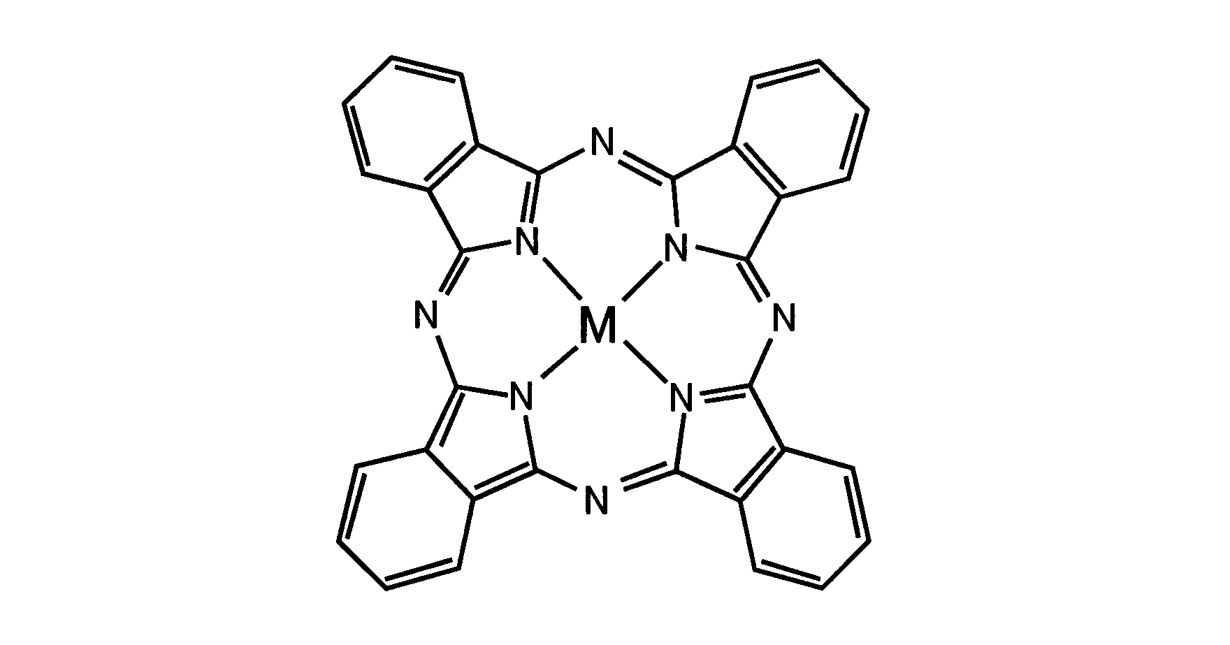

上述したフラーレン化合物には、置換基が付加されたフラーレン誘導体を含めてよい。当該置換基としては任意の基を適用できる。例えば、ハロゲン原子、アルキル基、アルケニル基、アルキニル基、アリール基、複素環基、シアノ基、ヒドロキシル基、ニトロ基、カルボキシル基、アルコキシ基、アリールオキシ基、シリルオキシ基、ヘテロ環オキシ基、アシルオキシ基、カルバモイルオキシ基、アルコキシカルボニルオキシ基、アリールオキシカルボニルオキシ基、アミノ基、アンモニオ基、アシルアミノ基、アミノカルボニルアミノ基、アルコキシカルボニルアミノ基、アリールオキシカルボニルアミノ基、スルファモイルアミノ基、アルキル及びアリールスルホニルアミノ基、メルカプト基、アルキルチオ基、アリールチオ基、ヘテロ環チオ基、スルファモイル基、スルホ基、アルキル及びアリールスルフィニル基、アルキル及びアリールスルホニル基、アシル基、アリールオキシカルボニル基、アルコキシカルボニル基、カルバモイル基、アリール及びヘテロ環アゾ基、イミド基、ホスフィノ基、ホスフィニル基、ホスフィニルオキシ基、ホスフィニルアミノ基、ホスホノ基、シリル基、ヒドラジノ基、ウレイド基、ボロン酸基、ホスファト基、スルファト基などが該当する。
上述したドナーとアクセプターの混合物以外では、単成分物質で形成してもよい。単成分物質は、例えば化学式(化4)に示す環状チアジルラジカル(BDTDA)のほか、N-エチルフェナジルなどが該当する。
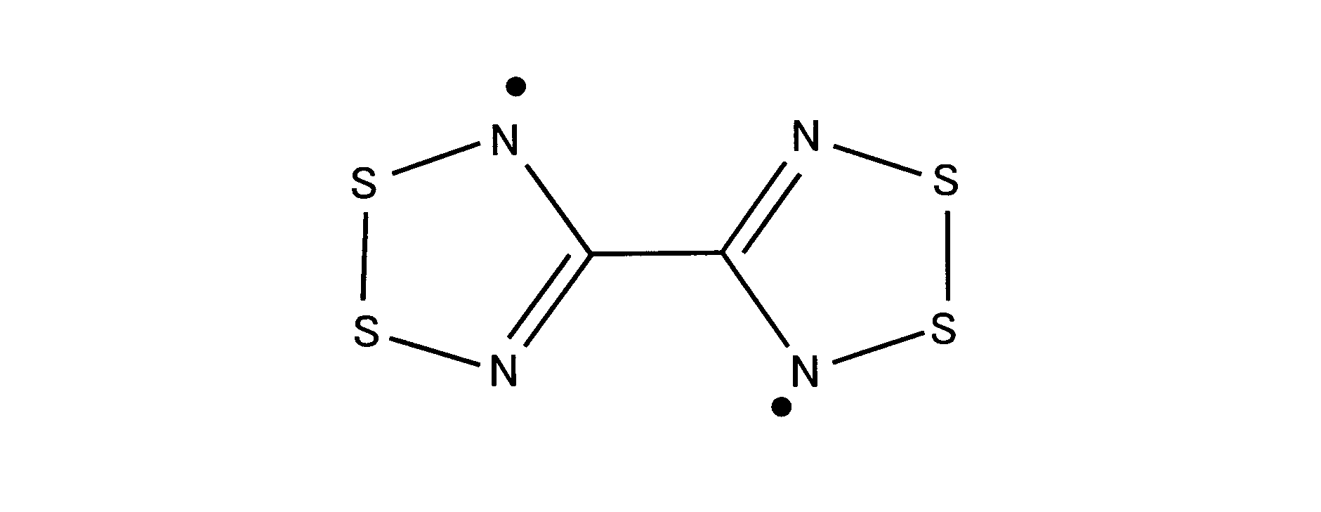
上記特定の波長域が赤外光(望ましくは近赤外光)の波長域である場合には、赤外光(もしくは近赤外光)に電荷移動吸収帯をもつ電荷移動錯体、あるいはそのドナーとアクセプターの混合物で形成する。ドナーとアクセプターの組み合わせは、上記条件を満たせば任意の物質を適用することができる。例えば、化学式(化5)の(A)に示すドナー側のテトラチアフルバレン(TTF)と、(B)に示すアクセプター側のクロラニル(CA)との組み合わせが該当する。同様に、化学式(化5)の(C)に示すドナー側の環状ジチアゾール化合物(NT)と、(D)に示すアクセプター側のテトラシアノキノジメタン(TCNQ)との組み合わせが該当する。
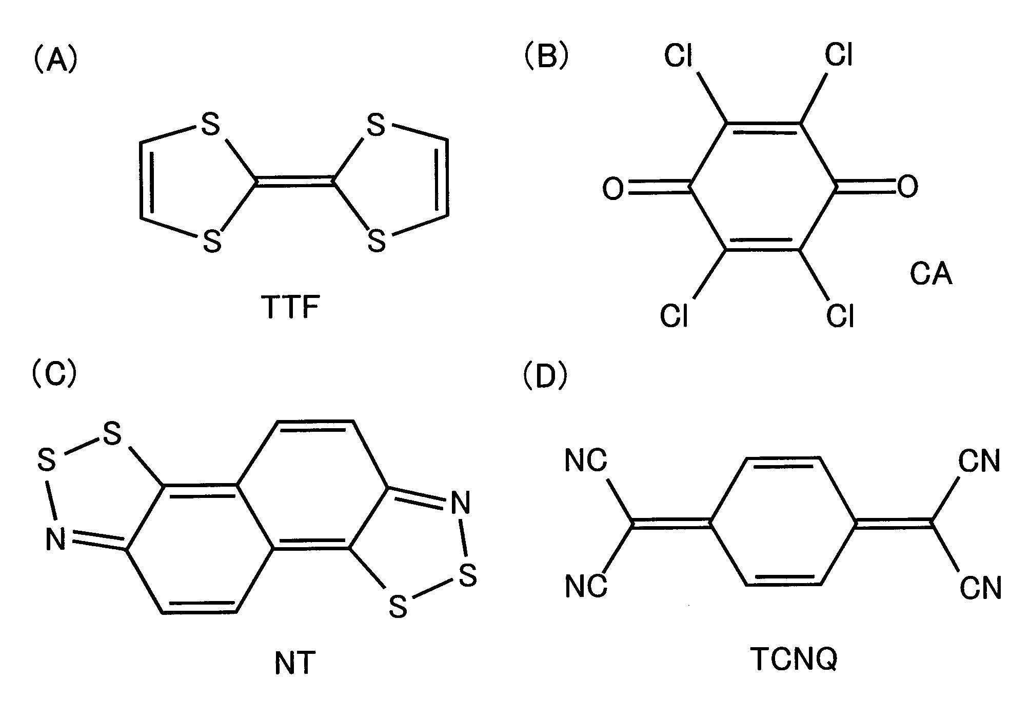
上述のように構成された有機光電変換素子10の作動原理について、図2を参照しながら説明する。なお、図2(A)は図1(A)の構造に対応し、図2(B)は図1(B)の構造に対応する。図2(A)と図2(B)とは構造が図面左右方向で逆になっているだけであるので、図2(A)の構造を例に説明する。
絶縁分極層13は100[nm]から1000[nm]の厚みがあるため、プラス(+)で図示するホールと、マイナス(-)で図示する電子とが矢印D1のように大きく分極する。電荷分離層14が光を受けると、エネルギー励起によって電荷分離が行われ、ホールと電子とが矢印D2のように分離する。分離したホールが絶縁分極層13を超えて第1電極11に移動しようとしても、厚みが大きいために移動できない。一方、分離した電子は隣接する第2電極15に矢印D3のように簡単に移動して吸収される。電荷分離は短時間で進行するので、第2電極15から短時間に多くの電子が流れ、結果として過渡電流が生じる。上記の作動は、仮に電荷分離層14にピンホールが存在しても同様である。
なお、図2(A)では電荷分離層14が光を直接的に受け、図2(B)では電荷分離層12が光を直接的に受けるが、光を間接的に受けてもよい。すなわち図2の左右側から光を受ける場合には、図2(A)では第2電極15、または、第1電極11および絶縁分極層13を透明材料で形成すればよい。図2(B)では第1電極11、または、絶縁分極層13および第2電極15を透明材料で形成すればよい。さらに、電極および絶縁分極層を不透明材料で形成する場合には、光が電荷分離層14に到達可能な厚みで形成すればよい。これらの材料や厚みは、後述する図3および図4にも同様に適用可能である。
上述した実施の形態1によれば、以下に示す各効果を得ることができる。まず請求項1に対応し、第1電極11と第2電極15とをそれぞれ仕事関数が異なる物質で形成し、電荷分離層(図1(A)では電荷分離層14、図1(B)では電荷分離層12)と絶縁分極層13とを隣接させる構造とした(図1を参照)。この構成によれば、一方の電極と電荷分離層との間に絶縁分極層13が介在するので、有機光電変換素子10の製造過程で仮にピンホールが発生したとしても、暗電流の発生が極力抑えられる。また、絶縁分極層13が分極することによって、電荷分離層中の電荷分離が促進される。分離後、電極に吸収された電荷は、電極間の仕事関数の差によって即座に他方の電極に移動するので、電荷分離層が光を受けてから電流が出力される応答性を従来よりも高めることができる。電荷分離は短時間で進行することから、高効率、高速、高SN比の過渡電流が得られる。また、後述するようにチョップ光(すなわち断続的なパルス波)を電荷分離層14に照射することによって交流信号を得ることもできる(図9を参照)。
請求項3に対応し、第1電極11と第2電極15とは、仕事関数に差がつくように、異なる物質で形成するか(表1を参照)、あるいは一方または双方の電極にバイアス電圧を印加する構成とした。この構成によれば、物質のコストや回路構成等に見合う適切な有機光電変換素子を製造することができる。
請求項4に対応し、第1電極11と第2電極15とは、仕事関数の差が0.1[eV]から3[eV]までの範囲とした。この構成によれば、電荷分離層で分離された電荷は隣接する電極に吸収され易くなるので、迅速かつ大きな過渡電流を発生させることができる。
請求項5に対応し、絶縁分極層13は、電荷分離層12,14よりも厚く形成した(図1,図2を参照)。この構成によれば、絶縁分極層13によってホールおよび電子の双方について移動が阻害されるので、暗電流の発生をより確実に抑えることができる。
請求項6に対応し、図1(A)に示す電荷分離層14または図1(B)に示す電荷分離層12は、いずれも1[nm]から50[nm]まで(好ましくは1[nm]から20[nm]まで、あるいは10[nm]から30[nm]まで)の厚さで形成した。この構成によれば、1[nm]から20[nm]までの厚さで形成することで、光を受けて電荷を分離し易くなり、かつ可能な限り大きな過渡電流を発生させることができる。また10[nm]から30[nm]までの厚さで形成することで、大きな電流量および高い量子効率の双方を確保することができる。
請求項7に対応し、絶縁分極層13は100[nm]から1000[nm]まで(好ましくは、100[nm]から300[nm]まで)の厚さで形成した。この構成によれば、適切な厚さで絶縁分極層13を形成することで、ホールおよび電荷の双方について移動を阻害して、暗電流の発生を確実に抑えることができる。
請求項8に対応し、受ける光の波長域に応じて電荷分離層12,14を形成する物質を異ならせる構成とした。この構成によれば、形成する物質を適切に選択することによって光吸収波長を制御することができ、可視・紫外・赤外の広い範囲で光-電流変換を実現することができる。このような広範囲の光の波長域であっても、より多くの電荷を分離することができる。
請求項9に対応し、特定の波長域にかかる光を受ける場合の電荷分離層12,14は、特定の波長域に吸収帯をもつドナーまたはアクセプター、特定の波長域に電荷移動吸収帯をもつドナーとアクセプターとの分子間化合物からなる電荷移動錯体、あるいはドナーとアクセプターとの混合物のいずれかで形成する構成とした。この構成によれば、特定の波長域の光を受けて、より多くの電荷を分離することができる。
請求項10に対応し、電荷分離層12,14は、特定の波長域は、可視光の波長域、紫外光の波長域、赤外光の波長域のうちで一以上の波長域とする物質で形成する構成とした。この構成によれば、可視光、紫外光、赤外光のうちで一以上の光を受けた電荷分離層12,14はより多くの電荷を分離することができる。
〔実施の形態2〕
実施の形態2は、対称構造の有機光電変換素子であって、図3と図4を参照しながら説明する。図3には本発明にかかる有機光電変換素子の第2構成例を断面図で示す。図4には図3に示す第2構成例の作動原理を模式図で示す。なお、図示および説明を簡単にするため、実施の形態2では実施の形態1と異なる点を説明する。よって実施の形態1で用いた要素と同一の要素には同一の符号を付して説明を省略する。
実施の形態2は、対称構造の有機光電変換素子であって、図3と図4を参照しながら説明する。図3には本発明にかかる有機光電変換素子の第2構成例を断面図で示す。図4には図3に示す第2構成例の作動原理を模式図で示す。なお、図示および説明を簡単にするため、実施の形態2では実施の形態1と異なる点を説明する。よって実施の形態1で用いた要素と同一の要素には同一の符号を付して説明を省略する。
図3に示す有機光電変換素子20の構造は、図1に示す有機光電変換素子10と比べて、有機層16の構成が相違する。すなわち、図1の有機層16は1つの電荷分離層(12または14)と1つの絶縁分極層13との組み合わせであるのに対して、図3の有機層16は2つの電荷分離層12,14と1つの絶縁分極層13との組み合わせである点が相違する。この構成では、絶縁分極層13が中央部に配置され、当該絶縁分極層13の両側に電荷分離層12,14が配置され、一番外側に第1電極11と第2電極15とが配置される。
上述のように構成された有機光電変換素子20の作動原理について、図4を参照しながら説明する。絶縁分極層13は上述したように100[nm]から1000[nm]の厚みがあるため、プラス(+)で図示するホールと、マイナス(-)で図示する電子とが矢印D1のように大きく分極する。なお「対称構造」はあくまで要素の対称性を意味し、電荷分離層12と電荷分離層14とで厚みを異ならせる場合(すなわちL1≠L3)を含む。
電荷分離層12,14でそれぞれ光を受けると、エネルギー励起によって電荷分離が行われ、ホールと電子とが矢印D2,D4のように分離する。電荷分離層12,14でそれぞれ分離した電荷が絶縁分極層13を超えて反対側の電極に移動しようとしても、厚みが大きいために移動できない。一方、電荷分離層12で分離したホールは隣接する第1電極11に矢印D5のように簡単に移動して吸収され、電荷分離層14で分離した電子は隣接する第2電極15に矢印D3のように簡単に移動して吸収される。電荷分離は短時間で進行するので、第2電極15から短時間に多くの電子が流れ、結果として過渡電流が生じる。上記の作動は、仮に電荷分離層12,14にピンホールが存在しても同様である。このように第1電極11および第2電極15の双方からホールや電子が流れるので、有機光電変換素子10に比べて大きな過渡電流が生じる。
上述した実施の形態2によれば、請求項2に対応し、有機層16は二つの電荷分離層12,14と、一つの絶縁分極層13とを有する構造とした(図3を参照)。この構成によれば、第1電極11および第2電極15の双方から電荷が流れるので、有機光電変換素子10に比べて大きな過渡電流が生じさせることができる。その他については実施の形態1と同様であるので、実施の形態1と同様の作用効果を得ることができる。
〔実施の形態3〕
実施の形態3は、図1に示す有機光電変換素子10を部分的に有する撮像素子であって、図5を参照しながら説明する。図5には撮像素子の構成例を断面図で示す。なお、図示および説明を簡単にするため、実施の形態3では実施の形態1と異なる点を説明する。よって実施の形態1で用いた要素と同一の要素には同一の符号を付して説明を省略する。また、画像または映像を単に「画像等」と表記する。
実施の形態3は、図1に示す有機光電変換素子10を部分的に有する撮像素子であって、図5を参照しながら説明する。図5には撮像素子の構成例を断面図で示す。なお、図示および説明を簡単にするため、実施の形態3では実施の形態1と異なる点を説明する。よって実施の形態1で用いた要素と同一の要素には同一の符号を付して説明を省略する。また、画像または映像を単に「画像等」と表記する。
図5に示す撮像素子30は、図1に示す有機光電変換素子10を部分的に備えるほか、光(特に可視光)を受けて1画素(1ピクセル)分の画像等の信号(いわゆる画像信号)として出力可能に構成されている。すなわち撮像素子30は、p型シリコン基板32をベースとし、有機光電変換素子10、絶縁膜31,37、n型不純物領域33,35、p型不純物領域34,36、n+型不純物領域38、接続部39などを有する構造となっている。これらのうちでn+型不純物領域38は、他の半導体領域に比べて不純物が高濃度となる領域である。
撮像素子30は、有機光電変換素子10の第2電極15側に、透明な絶縁膜31を介在させたうえでp型シリコン基板32を接合する。p型シリコン基板32は、絶縁膜31側から図面右側に向かって順番に、n+型不純物領域38、p型不純物領域36、n型不純物領域35、p型不純物領域34、n型不純物領域33が形成されている。絶縁膜31に貫通して形成された孔部には、第2電極15と接続される接続部39と、当該接続部39を囲んで絶縁膜31の周壁に接する絶縁膜37とが形成されている。接続部39は、第2電極15とn+型不純物領域38とを導通可能に接続する。
n型不純物領域35とp型不純物領域34との境界面はpn接合面となる。このpn接合面は、絶縁膜31とn型不純物領域35との境界面(以下では単に「基準面」と呼ぶ。)からの距離を、第1目的波長域(例えば可視光の青色)の光を吸収する長さ(例えば約0.2[μm])とする。n型不純物領域35とp型不純物領域34とは、第1目的波長域の光を吸収してそれに応じた電荷を蓄積する第1フォトダイオードとなる。当該第1フォトダイオードで発生した電荷は、n型不純物領域35に蓄積される。
n型不純物領域33とp型シリコン基板32との境界面もまたpn接合面となる。このpn接合面は、基準面からの距離を、第2目的波長域(例えば可視光の赤色)の光を吸収する長さ(例えば約2[μm])とする。n型不純物領域33とp型シリコン基板32とは、第2目的波長域の光を吸収してそれに応じた電荷を蓄積する第2フォトダイオードとなる。当該第2フォトダイオードで発生した電荷は、n型不純物領域33に蓄積される。
n+型不純物領域38は、接続部39を通じて第2電極15に接続されている。そのため、光を受けて電荷分離層14から第2電極15に吸収された電荷は、接続部39を通じてn+型不純物領域38に蓄積される。こうしてn+型不純物領域38は電荷を蓄積する点で「電荷蓄積部」に相当する。なお電荷分離層14は、図示するように直接的に光を受ける構造としてもよく、第1電極11および絶縁分極層13を透明物質で形成する場合には第1電極11側(図面左側)から間接的に光を受ける構造としてもよい。
n型不純物領域33に蓄積された電荷は、p型シリコン基板32内に形成されたnチャネルMOSトランジスタからなるMOS回路によってその電荷量に応じた信号に変換して出力される。n型不純物領域35に蓄積された電荷は、p型不純物領域34内に形成されたnチャネルMOSトランジスタからなるMOS回路によってその電荷量に応じた信号に変換して出力される。n+型不純物領域38に蓄積されている電荷は、p型不純物領域36内に形成されたnチャネルMOSトランジスタからなるMOS回路によってその電荷量に応じた信号に変換して出力される。上記の各MOS回路は一般的であるので図示を省略し、図示しない配線によって外部に信号を出力可能に構成される。なお、n型不純物領域33およびn型不純物領域35に引き出し電極を設けるのが望ましい。この引き出し電極に対して所定のリセット電位をかけると、各領域が空乏化するので、各pn接合部の容量は限りなく小さい値になる。したがって、各接合面に生じる容量を極めて小さくできる。
第2電極15,n+型不純物領域38,n型不純物領域35,n型不純物領域33のうちで一以上を信号出力回路(図示せず)に接続し、吸収または蓄積された電荷に応じた信号を読み出す。当該信号出力回路は、CMOS型またはCCD型で形成されるが、消費電力や読み出し速度等の観点ではCMOS型の方が好ましい。信号出力回路の駆動電圧(例えば約3[V]程度)に合わせて、消費電力を抑えるために電荷分離層14に印加する外部バイアス電圧も上記駆動電圧以下とするのが望ましい。
上述した実施の形態3によれば、以下に示す各効果を得ることができる。まず請求項11に対応し、撮像素子30は、有機光電変換素子10と、半導体基板に形成され、一以上の有機光電変換素子10で発生した電荷に応じた電流を読み出して外部に信号を出力するCMOS型又はCCD型の信号出力部とを有する構成とした(図5を参照)。この構成によれば、有機光電変換素子10(具体的には電荷分離層12,14)で発生した電荷に応じた電流が出力されると、当該電流を読み出した信号出力部が外部に信号を出力する。したがって、有機光電変換素子10の特性を有する撮像素子30を提供できる。
請求項12に対応し、半導体基板は、光を受けて有機光電変換素子10の電荷分離層12,14が分離した電荷を蓄積するn+型不純物領域38(電荷蓄積部)を有する構成とした(図5を参照)。この構成によれば、n+型不純物領域38は電荷分離層12,14が分離した電荷を蓄積するので、その後に蓄積した電荷を出力することができる。言い換えれば、電荷蓄積部は蓄電機能または充電機能を奏する部位である。電荷蓄積部を大きく形成すれば、蓄積後に大容量の電流を発生させることが可能になる。
その他の点については実施の形態1と同様であるので、実施の形態1と同様の作用効果を得ることができる。
〔実施の形態4〕
実施の形態4は、図3に示す有機光電変換素子20を部分的に有する撮像素子であって、図6を参照しながら説明する。図6には撮像素子の構成例を断面図で示す。なお、図示および説明を簡単にするため、実施の形態4では実施の形態3と異なる点を説明する。よって実施の形態3で用いた要素と同一の要素には同一の符号を付して説明を省略する。
実施の形態4は、図3に示す有機光電変換素子20を部分的に有する撮像素子であって、図6を参照しながら説明する。図6には撮像素子の構成例を断面図で示す。なお、図示および説明を簡単にするため、実施の形態4では実施の形態3と異なる点を説明する。よって実施の形態3で用いた要素と同一の要素には同一の符号を付して説明を省略する。
図6に示す撮像素子40は、図3に示す有機光電変換素子20を部分的に備えるほか、可視光を受けて1画素(1ピクセル)分の画像等の信号として出力可能に構成されている。すなわち撮像素子40は、p型シリコン基板32をベースとし、有機光電変換素子20、絶縁膜31,37、n型不純物領域33,35、p型不純物領域34,36、n+型不純物領域38、接続部39などを有する構造となっている。すなわち実施の形態3と比べると、有機光電変換素子10の代わりに有機光電変換素子20を用いた点が相違し、その他の点は同一である。したがって、有機光電変換素子20による固有の作用効果を除けば、実施の形態3および実施の形態2と同様の作用効果を得ることができる。
図6に示す撮像素子40は、1つの有機光電変換素子20を備えて、光(特に可視光)を受けて1画素分の画像等の信号として出力する構成とした。この構成に代えて、図示を省略するが、下記のような他の構成1~4の撮像素子40を製造することもできる。なお、光の三原色からの色選択はカラーフィルタやプリズム等を用いる。
(他の構成1)
p型シリコン基板32上には、1つの有機光電変換素子20と、2つのフォトダイオードとを形成する。1つの有機光電変換素子20の電荷分離層12(または電荷分離層14)は、光の三原色のうちで一色の波長域の光を受けて電荷を分離する。2つのフォトダイオードは、光の三原色のうちで残りの二色についてフォトダイオードごとに対応する色の波長域の光を受けて電荷を分離する。
p型シリコン基板32上には、1つの有機光電変換素子20と、2つのフォトダイオードとを形成する。1つの有機光電変換素子20の電荷分離層12(または電荷分離層14)は、光の三原色のうちで一色の波長域の光を受けて電荷を分離する。2つのフォトダイオードは、光の三原色のうちで残りの二色についてフォトダイオードごとに対応する色の波長域の光を受けて電荷を分離する。
(他の構成2)
p型シリコン基板32上には、2つの有機光電変換素子20と、1つのフォトダイオードとを形成する。2つの有機光電変換素子20の電荷分離層12(または電荷分離層14)は、光の三原色のうちで二色について対応する色の波長域の光を受けて電荷を分離する。1つのフォトダイオードは、光の三原色のうちで残りの一色の波長域の光を受けて電荷を分離する。
p型シリコン基板32上には、2つの有機光電変換素子20と、1つのフォトダイオードとを形成する。2つの有機光電変換素子20の電荷分離層12(または電荷分離層14)は、光の三原色のうちで二色について対応する色の波長域の光を受けて電荷を分離する。1つのフォトダイオードは、光の三原色のうちで残りの一色の波長域の光を受けて電荷を分離する。
(他の構成3)
p型シリコン基板32の表面側には、3つの有機光電変換素子20を形成する。3つの有機光電変換素子20は、光の三原色の各色ごとに対応する色の波長域の光を受けて電荷を分離する。
p型シリコン基板32の表面側には、3つの有機光電変換素子20を形成する。3つの有機光電変換素子20は、光の三原色の各色ごとに対応する色の波長域の光を受けて電荷を分離する。
(他の構成4)
有機光電変換素子20の電荷分離層12,14は、一方または双方の層が紫外または赤外(望ましくは近赤外)の波長域の光を受けて電荷を分離する物質で形成する。
有機光電変換素子20の電荷分離層12,14は、一方または双方の層が紫外または赤外(望ましくは近赤外)の波長域の光を受けて電荷を分離する物質で形成する。
上述した実施の形態1~4に対応する実施例を以下に示し、本発明をさらに具体的に説明する。各実施例を構造的に分類すると、実施例1~9は実施の形態1に対応し、実施例10~14は実施の形態2に対応する。さらに、実施例10~14に対する比較例1~3とを併せて示す。なお、本発明は各実施例には何ら限定されず、特許請求の範囲に記載された事項を満たす種々の変更を行うことが可能である。種々の変更を行った場合でも、上述した実施の形態1~4と同様の作用効果を得ることができる。
〔実施例1〕
透明導電膜として酸化インジウムスズ(以下では単に「ITO」と表記する。)からなる基板状の第1電極11の上面には、4×10⁻⁴[Pa]程度の真空中において電荷分離層12を形成した。この電荷分離層12は、有機ドナーとアクセプターが混在する領域であり、次の化学式(化6)に示すZn-フタロシアニン(以下では単に「ZnPc」と表記する。)と、化学式(化3)に示したフラーレンC60とが1:1となる共蒸着膜を1[Å/sec]の速度で堆積させて、厚さを50[nm]とした。電荷分離層12の上面には、ポリビニリデンジフルオライド(以下では単に「PVDF」と表記する。)のジメチルホルムアミド8%重量溶液をスピンコートした。絶縁分極層13の厚みが200[nm]であることを確認した。さらに絶縁分極層13の上面には、アルミニウム(以下では単に「Al」と表記する。)からなる第2電極15を厚さが60[nm]となるように蒸着した。第2電極15の有効面積は0.02[cm2]であった(以下の実施例2~14でも同様である)。
透明導電膜として酸化インジウムスズ(以下では単に「ITO」と表記する。)からなる基板状の第1電極11の上面には、4×10⁻⁴[Pa]程度の真空中において電荷分離層12を形成した。この電荷分離層12は、有機ドナーとアクセプターが混在する領域であり、次の化学式(化6)に示すZn-フタロシアニン(以下では単に「ZnPc」と表記する。)と、化学式(化3)に示したフラーレンC60とが1:1となる共蒸着膜を1[Å/sec]の速度で堆積させて、厚さを50[nm]とした。電荷分離層12の上面には、ポリビニリデンジフルオライド(以下では単に「PVDF」と表記する。)のジメチルホルムアミド8%重量溶液をスピンコートした。絶縁分極層13の厚みが200[nm]であることを確認した。さらに絶縁分極層13の上面には、アルミニウム(以下では単に「Al」と表記する。)からなる第2電極15を厚さが60[nm]となるように蒸着した。第2電極15の有効面積は0.02[cm2]であった(以下の実施例2~14でも同様である)。

〔実施例2〕
ITOの第1電極11を約100℃に熱しておき、絶縁分極層13としてPVDFのジメチルホルムアミド8%重量溶液をスピンコートした。絶縁分極層13の厚みが200[nm]となるようにスピンコートを調整した。絶縁分極層13上面に形成する電荷分離層14は、ドナーとアクセプターの共存層であり、4×10⁻⁴[Pa]程度の真空中において、上記化学式(化6)に示すZnPcと、化学式(化3)に示したフラーレンC60とが1:1となる共蒸着膜を1[Å/sec]の速度で堆積させて、厚さを50[nm]とした。さらに電荷分離層14の上面には、Alの第2電極15を厚さが60[nm]となるように蒸着した。
ITOの第1電極11を約100℃に熱しておき、絶縁分極層13としてPVDFのジメチルホルムアミド8%重量溶液をスピンコートした。絶縁分極層13の厚みが200[nm]となるようにスピンコートを調整した。絶縁分極層13上面に形成する電荷分離層14は、ドナーとアクセプターの共存層であり、4×10⁻⁴[Pa]程度の真空中において、上記化学式(化6)に示すZnPcと、化学式(化3)に示したフラーレンC60とが1:1となる共蒸着膜を1[Å/sec]の速度で堆積させて、厚さを50[nm]とした。さらに電荷分離層14の上面には、Alの第2電極15を厚さが60[nm]となるように蒸着した。
〔実施例3〕
ITOの第1電極11上面には、4×10⁻⁴[Pa]程度の真空中において電荷分離層12を形成した。この電荷分離層12は、ドナーであり、上記化学式(化6)に示すZnPcの蒸着膜を1[Å/sec]の速度で堆積させて、厚さを50[nm]とした。電荷分離層12の上面には、PVDFのジメチルホルムアミド8%重量溶液をスピンコートした。絶縁分極層13の厚みが200[nm]となるようにスピンコートを調整した。さらに絶縁分極層13の上面には、Alの第2電極15を厚さが50[nm]となるように蒸着した。
ITOの第1電極11上面には、4×10⁻⁴[Pa]程度の真空中において電荷分離層12を形成した。この電荷分離層12は、ドナーであり、上記化学式(化6)に示すZnPcの蒸着膜を1[Å/sec]の速度で堆積させて、厚さを50[nm]とした。電荷分離層12の上面には、PVDFのジメチルホルムアミド8%重量溶液をスピンコートした。絶縁分極層13の厚みが200[nm]となるようにスピンコートを調整した。さらに絶縁分極層13の上面には、Alの第2電極15を厚さが50[nm]となるように蒸着した。
〔実施例4〕
ITOの第1電極11を約100℃に熱しておき、絶縁分極層13としてPVDFのジメチルホルムアミド8%重量溶液をスピンコートした。絶縁分極層13の厚みが200[nm]となるようにスピンコートを調整した。絶縁分極層13上面に形成する電荷分離層14は、ドナーであり、4×10⁻⁴[Pa]程度の真空中において、上記化学式(化6)に示すZnPcからなる蒸着膜を1[Å/sec]の速度で堆積させて、厚さを50[nm]とした。さらに電荷分離層14の上面には、Alの第2電極15を厚さが60[nm]となるように蒸着した。
ITOの第1電極11を約100℃に熱しておき、絶縁分極層13としてPVDFのジメチルホルムアミド8%重量溶液をスピンコートした。絶縁分極層13の厚みが200[nm]となるようにスピンコートを調整した。絶縁分極層13上面に形成する電荷分離層14は、ドナーであり、4×10⁻⁴[Pa]程度の真空中において、上記化学式(化6)に示すZnPcからなる蒸着膜を1[Å/sec]の速度で堆積させて、厚さを50[nm]とした。さらに電荷分離層14の上面には、Alの第2電極15を厚さが60[nm]となるように蒸着した。
〔実施例5〕
ITOの第1電極11上面には、4×10⁻⁴[Pa]程度の真空中において電荷分離層12を形成した。この電荷分離層12は、アクセプターであり、上記化学式(化6)に示すC60の蒸着膜を1[Å/sec]の速度で堆積させて、厚さを50[nm]とした。電荷分離層12の上面には、PVDFのジメチルホルムアミド8%重量溶液をスピンコートした。絶縁分極層13の厚みが200[nm]となるようにスピンコートを調整した。さらに絶縁分極層13の上面には、Alの第2電極15を厚さが50[nm]となるように蒸着した。
ITOの第1電極11上面には、4×10⁻⁴[Pa]程度の真空中において電荷分離層12を形成した。この電荷分離層12は、アクセプターであり、上記化学式(化6)に示すC60の蒸着膜を1[Å/sec]の速度で堆積させて、厚さを50[nm]とした。電荷分離層12の上面には、PVDFのジメチルホルムアミド8%重量溶液をスピンコートした。絶縁分極層13の厚みが200[nm]となるようにスピンコートを調整した。さらに絶縁分極層13の上面には、Alの第2電極15を厚さが50[nm]となるように蒸着した。
〔実施例6〕
ITOの第1電極11を約100℃に熱しておき、絶縁分極層13としてPVDFのジメチルホルムアミド8%重量溶液をスピンコートした。絶縁分極層13の厚みが200[nm]となるようにスピンコートを調整した。絶縁分極層13上面に形成する電荷分離層14は、アクセプターであり、4×10⁻⁴[Pa]程度の真空中において、上記化学式(化6)に示すC60からなる蒸着膜を1[Å/sec]の速度で堆積させて、厚さを50[nm]とした。さらに電荷分離層14の上面には、Alの第2電極15を厚さが60[nm]となるように蒸着した。
ITOの第1電極11を約100℃に熱しておき、絶縁分極層13としてPVDFのジメチルホルムアミド8%重量溶液をスピンコートした。絶縁分極層13の厚みが200[nm]となるようにスピンコートを調整した。絶縁分極層13上面に形成する電荷分離層14は、アクセプターであり、4×10⁻⁴[Pa]程度の真空中において、上記化学式(化6)に示すC60からなる蒸着膜を1[Å/sec]の速度で堆積させて、厚さを50[nm]とした。さらに電荷分離層14の上面には、Alの第2電極15を厚さが60[nm]となるように蒸着した。
〔実施例7〕
ITOの第1電極11を約100℃に熱しておき、絶縁分極層13としてPVDFのジメチルホルムアミド8%重量溶液をスピンコートした。絶縁分極層13の厚みが200[nm]となるようにスピンコートを調整した。絶縁分極層13上面に形成する電荷分離層14は、ドナーとアクセプターが混在する層であり、4×10⁻⁴[Pa]程度の真空中において、上記化学式(化6)に示すZnPcと、化学式(化3)に示したフラーレンC60とが1:1となる共蒸着膜を1[Å/sec]の速度で堆積させて、厚さを50[nm]とした。さらに電荷分離層14の上面には、銀(Ag)からなる第2電極15を厚さが60[nm]となるように蒸着した。
ITOの第1電極11を約100℃に熱しておき、絶縁分極層13としてPVDFのジメチルホルムアミド8%重量溶液をスピンコートした。絶縁分極層13の厚みが200[nm]となるようにスピンコートを調整した。絶縁分極層13上面に形成する電荷分離層14は、ドナーとアクセプターが混在する層であり、4×10⁻⁴[Pa]程度の真空中において、上記化学式(化6)に示すZnPcと、化学式(化3)に示したフラーレンC60とが1:1となる共蒸着膜を1[Å/sec]の速度で堆積させて、厚さを50[nm]とした。さらに電荷分離層14の上面には、銀(Ag)からなる第2電極15を厚さが60[nm]となるように蒸着した。
〔実施例8〕
ITOの第1電極11を約100℃に熱しておき、絶縁分極層13としてPVDFのジメチルホルムアミド8%重量溶液をスピンコートした。絶縁分極層13の厚みが200[nm]となるようにスピンコートを調整した。絶縁分極層13上面に形成する電荷分離層14は、ドナーとアクセプターが混在する層であり、4×10⁻⁴[Pa]程度の真空中において、上記化学式(化6)に示すZnPcと、化学式(化3)に示したフラーレンC60とが1:1となる共蒸着膜を1[Å/sec]の速度で堆積させて、厚さを50[nm]とした。さらに電荷分離層14の上面には、銅(Cu)からなる第2電極15を厚さが60[nm]となるように蒸着した。
ITOの第1電極11を約100℃に熱しておき、絶縁分極層13としてPVDFのジメチルホルムアミド8%重量溶液をスピンコートした。絶縁分極層13の厚みが200[nm]となるようにスピンコートを調整した。絶縁分極層13上面に形成する電荷分離層14は、ドナーとアクセプターが混在する層であり、4×10⁻⁴[Pa]程度の真空中において、上記化学式(化6)に示すZnPcと、化学式(化3)に示したフラーレンC60とが1:1となる共蒸着膜を1[Å/sec]の速度で堆積させて、厚さを50[nm]とした。さらに電荷分離層14の上面には、銅(Cu)からなる第2電極15を厚さが60[nm]となるように蒸着した。
〔実施例9〕
ITOの第1電極11を約100℃に熱しておき、絶縁分極層13としてPVDFのジメチルホルムアミド8%重量溶液をスピンコートした。絶縁分極層13の厚みが200[nm]となるようにスピンコートを調整した。絶縁分極層13上面に形成する電荷分離層14は、ドナーとアクセプターが混在する層であり、1×10⁻³[Pa]程度の真空中において、次の化学式(化7)に示すビス(4-ジメチルアミノジチオベンジル)ニッケル(II)からなる蒸着膜を0.5[Å/sec]の速度で堆積させて、厚さを50[nm]とした。さらに電荷分離層14の上面には、銀(Ag)からなる第2電極15を厚さが50[nm]となるように蒸着した。なお、上記ビス(4-ジメチルアミノジチオベンジル)ニッケル(II)は、後述する図7(A)における実施例9の欄では「BDN」と示す。
ITOの第1電極11を約100℃に熱しておき、絶縁分極層13としてPVDFのジメチルホルムアミド8%重量溶液をスピンコートした。絶縁分極層13の厚みが200[nm]となるようにスピンコートを調整した。絶縁分極層13上面に形成する電荷分離層14は、ドナーとアクセプターが混在する層であり、1×10⁻³[Pa]程度の真空中において、次の化学式(化7)に示すビス(4-ジメチルアミノジチオベンジル)ニッケル(II)からなる蒸着膜を0.5[Å/sec]の速度で堆積させて、厚さを50[nm]とした。さらに電荷分離層14の上面には、銀(Ag)からなる第2電極15を厚さが50[nm]となるように蒸着した。なお、上記ビス(4-ジメチルアミノジチオベンジル)ニッケル(II)は、後述する図7(A)における実施例9の欄では「BDN」と示す。
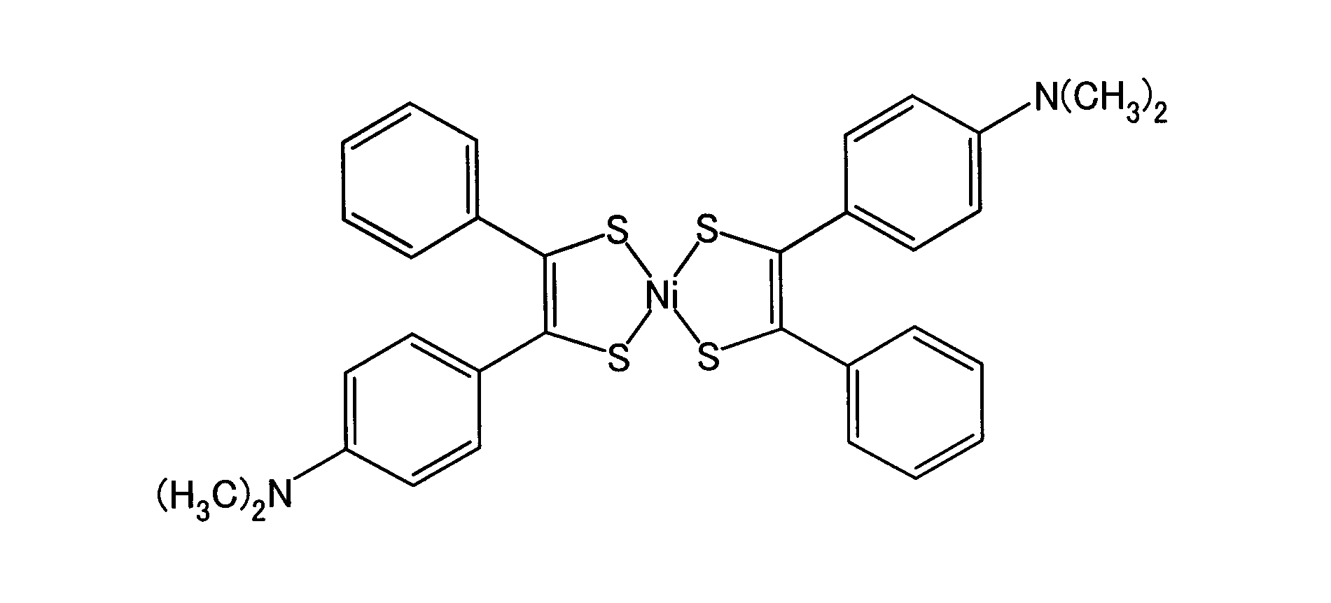
〔実施例10〕
ITOの第1電極11上面には、4×10⁻⁴[Pa]程度の真空中において電荷分離層12を形成した。この電荷分離層12は、ドナーとアクセプターが混在する層であり、上記化学式(化6)に示すZnPcと、化学式(化3)に示したフラーレンC60とが1:1となる共蒸着膜を1[Å/sec]の速度で堆積させて、厚さを50[nm]とした。電荷分離層12の上面には、PVDFのジメチルホルムアミド8%重量溶液をスピンコートした。絶縁分極層13の厚みが200[nm]となるようにスピンコートを調整した。絶縁分極層13の上面に形成する電荷分離層14は、電荷分離層12の場合と同様に堆積させて、厚さを50[nm]とした。さらに電荷分離層14の上面には、Alの第2電極15を厚さが60[nm]となるように蒸着した。
ITOの第1電極11上面には、4×10⁻⁴[Pa]程度の真空中において電荷分離層12を形成した。この電荷分離層12は、ドナーとアクセプターが混在する層であり、上記化学式(化6)に示すZnPcと、化学式(化3)に示したフラーレンC60とが1:1となる共蒸着膜を1[Å/sec]の速度で堆積させて、厚さを50[nm]とした。電荷分離層12の上面には、PVDFのジメチルホルムアミド8%重量溶液をスピンコートした。絶縁分極層13の厚みが200[nm]となるようにスピンコートを調整した。絶縁分極層13の上面に形成する電荷分離層14は、電荷分離層12の場合と同様に堆積させて、厚さを50[nm]とした。さらに電荷分離層14の上面には、Alの第2電極15を厚さが60[nm]となるように蒸着した。
〔実施例11〕
ITOの第1電極11上面には、4×10⁻⁴[Pa]程度の真空中において電荷分離層12を形成した。この電荷分離層12は、ドナーとアクセプターが混在する層であり、上記化学式(化6)に示すZnPcと、化学式(化3)に示したフラーレンC60とが1:1となる共蒸着膜を1[Å/sec]の速度で堆積させて、厚さを100[nm]とした。電荷分離層12の上面には、PVDFのジメチルホルムアミド8%重量溶液をスピンコートした。絶縁分極層13の厚みが200[nm]となるようにスピンコートを調整した。絶縁分極層13の上面に形成する電荷分離層14は、電荷分離層12の場合と同様に堆積させて、厚さを100[nm]とした。さらに電荷分離層14の上面には、Alの第2電極15を厚さが60[nm]となるように蒸着した。
ITOの第1電極11上面には、4×10⁻⁴[Pa]程度の真空中において電荷分離層12を形成した。この電荷分離層12は、ドナーとアクセプターが混在する層であり、上記化学式(化6)に示すZnPcと、化学式(化3)に示したフラーレンC60とが1:1となる共蒸着膜を1[Å/sec]の速度で堆積させて、厚さを100[nm]とした。電荷分離層12の上面には、PVDFのジメチルホルムアミド8%重量溶液をスピンコートした。絶縁分極層13の厚みが200[nm]となるようにスピンコートを調整した。絶縁分極層13の上面に形成する電荷分離層14は、電荷分離層12の場合と同様に堆積させて、厚さを100[nm]とした。さらに電荷分離層14の上面には、Alの第2電極15を厚さが60[nm]となるように蒸着した。
〔実施例12〕
ITOの第1電極11上面には、4×10⁻⁴[Pa]程度の真空中において電荷分離層12を形成した。この電荷分離層12は、ドナーとアクセプターが混在する層であり、上記化学式(化6)に示すZnPcと、化学式(化3)に示したフラーレンC60とが1:1となる共蒸着膜を1[Å/sec]の速度で堆積させて、厚さを25[nm]とした。電荷分離層12の上面には、PVDFのジメチルホルムアミド8%重量溶液をスピンコートした。絶縁分極層13の厚みが200[nm]となるようにスピンコートを調整した。絶縁分極層13の上面に形成する電荷分離層14は、電荷分離層12の場合と同様に堆積させて、厚さを25[nm]とした。さらに電荷分離層14の上面には、Alの第2電極15を厚さが60[nm]となるように蒸着した。
ITOの第1電極11上面には、4×10⁻⁴[Pa]程度の真空中において電荷分離層12を形成した。この電荷分離層12は、ドナーとアクセプターが混在する層であり、上記化学式(化6)に示すZnPcと、化学式(化3)に示したフラーレンC60とが1:1となる共蒸着膜を1[Å/sec]の速度で堆積させて、厚さを25[nm]とした。電荷分離層12の上面には、PVDFのジメチルホルムアミド8%重量溶液をスピンコートした。絶縁分極層13の厚みが200[nm]となるようにスピンコートを調整した。絶縁分極層13の上面に形成する電荷分離層14は、電荷分離層12の場合と同様に堆積させて、厚さを25[nm]とした。さらに電荷分離層14の上面には、Alの第2電極15を厚さが60[nm]となるように蒸着した。
〔実施例13〕
ITOの第1電極11上面には、4×10⁻⁴[Pa]程度の真空中において電荷分離層12を形成した。この電荷分離層12は、ドナーとアクセプターが混在する層であり、上記化学式(化6)に示すZnPcと、化学式(化3)に示したフラーレンC60とが1:1となる共蒸着膜を1[Å/sec]の速度で堆積させて、厚さを50[nm]とした。電荷分離層12の上面には、PVDFのジメチルホルムアミド8%重量溶液をスピンコートした。絶縁分極層13の厚みが100[nm]となるようにスピンコートを調整した。絶縁分極層13の上面に形成する電荷分離層14は、電荷分離層12の場合と同様に堆積させて、厚さを50[nm]とした。さらに電荷分離層14の上面には、Alの第2電極15を厚さが60[nm]となるように蒸着した。
ITOの第1電極11上面には、4×10⁻⁴[Pa]程度の真空中において電荷分離層12を形成した。この電荷分離層12は、ドナーとアクセプターが混在する層であり、上記化学式(化6)に示すZnPcと、化学式(化3)に示したフラーレンC60とが1:1となる共蒸着膜を1[Å/sec]の速度で堆積させて、厚さを50[nm]とした。電荷分離層12の上面には、PVDFのジメチルホルムアミド8%重量溶液をスピンコートした。絶縁分極層13の厚みが100[nm]となるようにスピンコートを調整した。絶縁分極層13の上面に形成する電荷分離層14は、電荷分離層12の場合と同様に堆積させて、厚さを50[nm]とした。さらに電荷分離層14の上面には、Alの第2電極15を厚さが60[nm]となるように蒸着した。
〔実施例14〕
ITOの第1電極11上面には、4×10⁻⁴[Pa]程度の真空中において電荷分離層12を形成した。この電荷分離層12は、ドナーとアクセプターが混在する層であり、上記化学式(化6)に示すZnPcと、化学式(化3)に示したフラーレンC60とが1:1となる共蒸着膜を1[Å/sec]の速度で堆積させて、厚さを50[nm]とした。電荷分離層12の上面には、PVDFのジメチルホルムアミド8%重量溶液をスピンコートした。絶縁分極層13の厚みが400[nm]となるようにスピンコートを調整した。絶縁分極層13の上面に形成する電荷分離層14は、電荷分離層12の場合と同様に堆積させて、厚さを50[nm]とした。さらに電荷分離層14の上面には、Alの第2電極15を厚さが60[nm]となるように蒸着した。
ITOの第1電極11上面には、4×10⁻⁴[Pa]程度の真空中において電荷分離層12を形成した。この電荷分離層12は、ドナーとアクセプターが混在する層であり、上記化学式(化6)に示すZnPcと、化学式(化3)に示したフラーレンC60とが1:1となる共蒸着膜を1[Å/sec]の速度で堆積させて、厚さを50[nm]とした。電荷分離層12の上面には、PVDFのジメチルホルムアミド8%重量溶液をスピンコートした。絶縁分極層13の厚みが400[nm]となるようにスピンコートを調整した。絶縁分極層13の上面に形成する電荷分離層14は、電荷分離層12の場合と同様に堆積させて、厚さを50[nm]とした。さらに電荷分離層14の上面には、Alの第2電極15を厚さが60[nm]となるように蒸着した。
〔実施例15〕
実施例1~9に示す有機光電変換素子10を用いてバイアス回路を構成すると、図13のようになる。有機光電変換素子10は、第1電極11をITOで形成し、絶縁分極層13をPVDFで形成し、電荷分離層14を次の化学式(化8)に示すLi-フタロシアニン(以下では単に「LiPc」と表記する。)からなる蒸着膜で形成し、第2電極15をAlで形成する。電荷分離層12,14に照射する光には、波長が532[nm],強度が4[mW/cm2]からなるCWレーザーを用いる。
実施例1~9に示す有機光電変換素子10を用いてバイアス回路を構成すると、図13のようになる。有機光電変換素子10は、第1電極11をITOで形成し、絶縁分極層13をPVDFで形成し、電荷分離層14を次の化学式(化8)に示すLi-フタロシアニン(以下では単に「LiPc」と表記する。)からなる蒸着膜で形成し、第2電極15をAlで形成する。電荷分離層12,14に照射する光には、波長が532[nm],強度が4[mW/cm2]からなるCWレーザーを用いる。

図13に示す回路図では、第1電極11と第2電極15との間に電流計60およびバッテリEを接続する。電流計60はバイアス特性を測定するための測定器である。バッテリEは、有機光電変換素子10に対してバイアスをかけるための電力源である。バッテリEのプラス端子を第1電極11側に接続し、マイナス端子を第2電極15側に接続する。バッテリEの電圧を-5[V],0[V],+5[V]としたときの各特性を図14に示す。図14のバイアス特性から明らかなように、バイアス電圧がプラス方向に高くなるにつれて、光電流(Photocurrent)も大きくなることが分かる。なお図示しないが、LiPc以外であって電荷分離層14に適用可能な材料で電荷分離層14を形成した有機光電変換素子10や、実施例10~14に示す有機光電変換素子20を用いて、図13と同様のバイアス回路を構成する場合も同様のバイアス特性が得られる。
〔比較例1〕
ITOの第1電極11上面には、4×10⁻⁴[Pa]程度の真空中において電荷分離層12を形成した。この電荷分離層12は、ドナーとアクセプターが混在する層であり、上記化学式(化6)に示すZnPcと、化学式(化3)に示したフラーレンC60とが1:1となる共蒸着膜を1[Å/sec]の速度で堆積させて、厚さを0.2[nm]とした。電荷分離層12の上面には、PVDFのジメチルホルムアミド8%重量溶液をスピンコートした。絶縁分極層13の厚みが200[nm]となるようにスピンコートを調整した。絶縁分極層13の上面に形成する電荷分離層14は、電荷分離層12の場合と同様に堆積させて、厚さを0.2[nm]とした。さらに電荷分離層14の上面には、Alの第2電極15を厚さが60[nm]となるように蒸着した。
ITOの第1電極11上面には、4×10⁻⁴[Pa]程度の真空中において電荷分離層12を形成した。この電荷分離層12は、ドナーとアクセプターが混在する層であり、上記化学式(化6)に示すZnPcと、化学式(化3)に示したフラーレンC60とが1:1となる共蒸着膜を1[Å/sec]の速度で堆積させて、厚さを0.2[nm]とした。電荷分離層12の上面には、PVDFのジメチルホルムアミド8%重量溶液をスピンコートした。絶縁分極層13の厚みが200[nm]となるようにスピンコートを調整した。絶縁分極層13の上面に形成する電荷分離層14は、電荷分離層12の場合と同様に堆積させて、厚さを0.2[nm]とした。さらに電荷分離層14の上面には、Alの第2電極15を厚さが60[nm]となるように蒸着した。
〔比較例2〕
ITOの第1電極11上面には、4×10⁻⁴[Pa]程度の真空中において電荷分離層12を形成した。この電荷分離層12は、ドナーとアクセプターが混在する層であり、上記化学式(化6)に示すZnPcと、化学式(化3)に示したフラーレンC60とが1:1となる共蒸着膜を1[Å/sec]の速度で堆積させて、厚さを50[nm]とした。電荷分離層12の上面には、PVDFのジメチルホルムアミド8%重量溶液をスピンコートした。絶縁分極層13の厚みが1[nm]となるようにスピンコートを調整した。絶縁分極層13の上面に形成する電荷分離層14は、電荷分離層12の場合と同様に堆積させて、厚さを50[nm]とした。さらに電荷分離層14の上面には、Alの第2電極15を厚さが60[nm]となるように蒸着した。
ITOの第1電極11上面には、4×10⁻⁴[Pa]程度の真空中において電荷分離層12を形成した。この電荷分離層12は、ドナーとアクセプターが混在する層であり、上記化学式(化6)に示すZnPcと、化学式(化3)に示したフラーレンC60とが1:1となる共蒸着膜を1[Å/sec]の速度で堆積させて、厚さを50[nm]とした。電荷分離層12の上面には、PVDFのジメチルホルムアミド8%重量溶液をスピンコートした。絶縁分極層13の厚みが1[nm]となるようにスピンコートを調整した。絶縁分極層13の上面に形成する電荷分離層14は、電荷分離層12の場合と同様に堆積させて、厚さを50[nm]とした。さらに電荷分離層14の上面には、Alの第2電極15を厚さが60[nm]となるように蒸着した。
〔比較例3〕
ITOの第1電極11上面には、4×10⁻⁴[Pa]程度の真空中において電荷分離層12を形成した。この電荷分離層12は、ドナーとアクセプターが混在する層であり、上記化学式(化6)に示すZnPcと、化学式(化3)に示したフラーレンC60とが1:1となる共蒸着膜を1[Å/sec]の速度で堆積させて、厚さを50[nm]とした。電荷分離層12の上面には、PVDFのジメチルホルムアミド8%重量溶液をスピンコートした。絶縁分極層13の厚みが2000[nm]となるようにスピンコートを調整した。絶縁分極層13の上面に形成する電荷分離層14は、電荷分離層12の場合と同様に堆積させて、厚さを50[nm]とした。さらに電荷分離層14の上面には、Alの第2電極15を厚さが60[nm]となるように蒸着した。
ITOの第1電極11上面には、4×10⁻⁴[Pa]程度の真空中において電荷分離層12を形成した。この電荷分離層12は、ドナーとアクセプターが混在する層であり、上記化学式(化6)に示すZnPcと、化学式(化3)に示したフラーレンC60とが1:1となる共蒸着膜を1[Å/sec]の速度で堆積させて、厚さを50[nm]とした。電荷分離層12の上面には、PVDFのジメチルホルムアミド8%重量溶液をスピンコートした。絶縁分極層13の厚みが2000[nm]となるようにスピンコートを調整した。絶縁分極層13の上面に形成する電荷分離層14は、電荷分離層12の場合と同様に堆積させて、厚さを50[nm]とした。さらに電荷分離層14の上面には、Alの第2電極15を厚さが60[nm]となるように蒸着した。
上述した実施例1~14および比較例1~3において、第1電極11と第2電極15とを導線で直結し、ゼロバイアス電圧下状態とする。また、電荷分離層12,14に照射する光には、波長が532[nm],周波数が1000[Hz],強度が31.8[mW/cm2]からなるCWレーザーを用いる。このCWレーザーを電荷分離層12,14に照射したときに生じる過渡電流値(ピーク値)を図7に示す。図7(A)の表には、実施の形態1(非対称構造の有機光電変換素子10)に対応する実施例1~9の結果を示す。図7(B)の表には、実施の形態2(対称構造の有機光電変換素子20)に対応する実施例10~14および比較例1~3の結果を示す。強度が31.8[mW/cm2]のときに生じる過渡電流は、系の抵抗とキャパシタンスによって変わるものの、ピーク値に達するまでの立ち上がり速度は7[ns]以下であり、定常値までに戻る回復時間は1[μs]であった。これはバンド幅が160[kHz]に相当することを意味する。また、暗電流は10-12[A]以下であり、ピーク時における内部量子効率は70%以上であり、交流のRMS値は35%以上であった。なお、過渡電流値(ピーク値)として示す「0.01[nA]以下」は計測機器による検出限界以下であることを意味する。
上記CWレーザーの波長と周波数は変えずに、強度を変えた場合の変化を図8に示す。図8にはレーザー光の有無(On/Off)に対する電流密度(Current density)の経時的変化をグラフで示す。この変化から明らかなように、CWレーザーの強度が強まるにつれて、過渡電流の電流密度もまた高まっている。また、CWレーザーを照射し始めると電流密度がプラス方向に変化するが、CWレーザーの照射を止めると電流密度がマイナス方向に変化する。これは、CWレーザーが照射されている間は一方の電極(例えば第2電極15)に吸収された電荷が導線を移動して第1電極11に蓄積されるが、CWレーザーの照射が止むと蓄積された第1電極11の電荷が導線を移動して第2電極15に戻ることを示している。このように、第1電極11と第2電極15とを接続(直接/間接を問わない)すると、1回の光照射で1つの交流波形が発生することを意味する。
チョップ光(すなわち断続的なパルス波)のようにCWレーザーの照射(On)と非照射(Off)とを繰り返し行うと、過渡電流(電流密度)は図9に示すように変化する。図9から明らかなように、過渡電流が照射/非照射に伴って変化しており、しかもピーク値がほぼ一定に保たれていることが分かる。
CWレーザーの周波数および強度を一定とし、波長を変化させた場合における過渡電流の変化を図10に示す。図10は電荷分離層12,14にZnPcとフラーレンC60との共蒸着膜を用いた有機光電変換素子10,20の例を示す。この図10は、光の波長(Wavelength)に対し、吸収スペクトル(Absorption spectrum)と、過渡電流に相当する光電流(Photocurrent)の変化をグラフで示す。図10から明らかなように、吸収スペクトルは400[nm]付近で最大になる反面、光電流は620[nm]付近で最大になる。なお、電荷分離層12,14にZnPcを用いた有機光電変換素子10,20は別の特性を示す。すなわち、電荷分離層12,14としてどのような物質を用いるかによって特性が変化する。
CWレーザーの光強度(Light intensity)を一定とし、電流密度(Current density)を変化させた場合における過渡電流にかかる立ち上がり時間(Rise
time)の変化を図11に示す。図11には、立ち上がり時間と電流密度との関係を「△」でプロットして示す。図11から明らかなように、電流密度が高まるにつれて、立ち上がり時間が短くなっている。したがって、応答速度を高めるには電流密度をより高めることが望ましい。すなわち、より強い光を照射することが望ましい。
time)の変化を図11に示す。図11には、立ち上がり時間と電流密度との関係を「△」でプロットして示す。図11から明らかなように、電流密度が高まるにつれて、立ち上がり時間が短くなっている。したがって、応答速度を高めるには電流密度をより高めることが望ましい。すなわち、より強い光を照射することが望ましい。
照射する光の条件を一定として、絶縁分極層13を形成する物質を異ならせた場合における過渡電流の変化を図12に示す。図12には、光の有無(On/Off)に対し、過渡電流に相当する電流密度(Current density)の経時的変化をグラフで示す。具体的には、PVDFで形成した例を図12(A)に示し、ポリスチレンで形成した例を図12(B)に示し、真空の空間で形成した例を図12(C)に示す。図12から明らかなように、絶縁分極層13を形成する物質が変わっても、ノイズレベルと比較して、オン/オフ時の判断は容易に行える。ただ、過渡電流のピーク値が物質に応じて大きく変化する。このことから、有機光電変換素子10,20の使用目的やコスト等を考慮して、電荷分離層12,14を形成する適切な物質を選択する必要がある。
CWレーザーの波長域を近赤外光として照射する場合における過渡電流の変化ついて、図15と図16を参照しながら説明する。図15には、有機光電変換素子の出力特性を測定するための回路図を示す。図16には、図15の回路図による出力特性をグラフ図で示す。図15に示す回路図では、第1電極11と第2電極15との間に抵抗器Rを接続し、当該抵抗器Rの両端に電圧計50を接続する。近赤外光としての波長を1064[nm]とし、周波数を1000[Hz]とするCWレーザーの照射方向を矢印で示す。電圧計50によって計測されるのは、過渡電流に相当する光電圧(Photovoltage)である。この光電圧は、図16に示すような経時的変化をする。抵抗器Rの抵抗値は1[MΩ]であるので、過渡電流のピーク値は3.70[nA]ほどになる。このことから、近赤外光として照射する場合でも確実に過渡電流を発生させることができる。
電荷分離層12,14の膜厚依存性について、図17と図18を参照しながら説明する。図17には、電荷分離層の膜厚依存性を調べるための回路図を示す。図18には、図17の回路図による膜厚依存性をグラフ図で示す。具体的には、電流密度(Current density)の経時的変化を図18(A)に示し、電荷分離層の膜厚に対する外部量子効率(EQE)の変化を図18(B)に示し、電荷分離層の膜厚に対する内部量子効率(IQE)の変化を図18(C)に示す。なお図18(A)では、膜厚ごとの電流密度の変化が分かるように、CWレーザーの照射時期(onとoffのタイミング)をずらしている。図18(B)と図18(C)とに示す量子化効率は、所定膜厚(本例では50[nm])で規格化(Normalized)した値でプロットしている。
図17に示す回路図は、一例として図1(A)に示す有機光電変換素子10を適用し、第1電極11と第2電極15との間に電流計60を接続する。有機光電変換素子10は、上述した実施例と同様にして構成する。すなわち、第1電極11をITOで形成し、絶縁分極層13をPVDFで形成し、電荷分離層14をZnPcとフラーレンC60との共蒸着膜で形成し、第2電極15をAlで形成する。絶縁分極層13の膜厚L2は200[nm]である。この条件下において、電荷分離層14の膜厚L3を5,10,25,50[nm]で変化させると、図18に示すような特性が得られる。
図18(A)に示す変化によれば、電荷分離層14の膜厚L3が厚くなるにつれて、電流密度(すなわち電流量)が増加する。図18(B)に示す変化によれば、膜厚L3が厚くなるにつれて、外部量子効率が高まる。これに対して図18(C)に示す変化によれば、膜厚L3が厚くなるにつれて、内部量子効率は一旦高くなるが、10~30[nm]が最大になり、これを超えると逆に内部量子効率は低くなる。このことから、膜厚L3を増加させてゆくと、一旦は電流量や量子効率が増加するものの、所定厚さを超えると量子効率が悪化する。したがって、大きな電流量および高い量子効率の双方を確保するには、電荷分離層14の膜厚L3を10~30[nm]で形成するのが望ましい。本例では図1(A)に示す有機光電変換素子10を適用する場合を説明したが、図1(B)に示す有機光電変換素子10を適用する場合や、図3に示す有機光電変換素子20を適用する場合でも、図18と同様の特性が得られる。また、絶縁分極層13を100[nm]から1000[nm]の範囲であって、200[nm]以外の厚みで形成する場合でも、図18と同様の特性が得られる。
なお上述した実施例1~14では、第1電極11としてITOを用い、第2電極15としてAl,Ag,Cuを用いた。仕事関数に0.1[eV]から3[eV]までの範囲で差がつくように、第1電極11や第2電極15に他の物質を用いてもよい。他の物質は、例えば表1に示す物質に限らず、表1以外の金属や、金属酸化物、金属と有機物との化合物等が該当する。こうした他の物質を電極として用いた場合であっても、上述した実施例1~14と同等の過渡電流が生じる。
〔他の発明の態様〕
以上では本発明を実施するための形態について説明したが、この形態には特許請求の範囲に記載した発明の態様以外の発明の態様を有するものである。この発明の態様を以下に列挙するとともに、必要に応じて関連説明を行う。
以上では本発明を実施するための形態について説明したが、この形態には特許請求の範囲に記載した発明の態様以外の発明の態様を有するものである。この発明の態様を以下に列挙するとともに、必要に応じて関連説明を行う。
〔態様1〕前記半導体基板は、1つの前記有機光電変換素子と、2つのフォトダイオードとが形成され、
1つの前記有機光電変換素子の前記電荷分離層は、光の三原色のうちで一色の波長域の光を受けて電荷を分離し、
2つの前記フォトダイオードは、前記光の三原色のうちで残りの二色について前記フォトダイオードごとに対応する色の波長域の光を受けて電荷を分離する構成としたことを特徴とする請求項11または12に記載の撮像素子。
〔態様1の関連説明〕光の三原色のうちで二色をフォトダイオードが受けて電流に変換し、一色を有機光電変換素子20が受けて電流に変換する。三色ともフォトダイオードを用いて過渡電流に変換するように構成された素子と比べると、暗電流の発生が抑制されるので、色合いを向上させることができる。
1つの前記有機光電変換素子の前記電荷分離層は、光の三原色のうちで一色の波長域の光を受けて電荷を分離し、
2つの前記フォトダイオードは、前記光の三原色のうちで残りの二色について前記フォトダイオードごとに対応する色の波長域の光を受けて電荷を分離する構成としたことを特徴とする請求項11または12に記載の撮像素子。
〔態様1の関連説明〕光の三原色のうちで二色をフォトダイオードが受けて電流に変換し、一色を有機光電変換素子20が受けて電流に変換する。三色ともフォトダイオードを用いて過渡電流に変換するように構成された素子と比べると、暗電流の発生が抑制されるので、色合いを向上させることができる。
〔態様2〕前記半導体基板は、2つの前記有機光電変換素子と、1つのフォトダイオードとが形成され、
2つの前記有機光電変換素子の前記電荷分離層は、光の三原色のうちで二色について前記半導体ごとに対応する色の波長域の光を受けて電荷を分離し、
1つの前記フォトダイオードは、前記光の三原色のうちで残りの一色の波長域の光を受けて電荷を分離する構成としたことを特徴とする請求項11または12に記載の撮像素子。
〔態様2の関連説明〕光の三原色のうちで一色をフォトダイオードが受けて電流に変換し、二色を有機光電変換素子20が受けて電流に変換する。三色ともフォトダイオードを用いて過渡電流に変換するように構成された素子と比べると、暗電流の発生がさらに抑制されるので、色合いをより向上させることができる。
2つの前記有機光電変換素子の前記電荷分離層は、光の三原色のうちで二色について前記半導体ごとに対応する色の波長域の光を受けて電荷を分離し、
1つの前記フォトダイオードは、前記光の三原色のうちで残りの一色の波長域の光を受けて電荷を分離する構成としたことを特徴とする請求項11または12に記載の撮像素子。
〔態様2の関連説明〕光の三原色のうちで一色をフォトダイオードが受けて電流に変換し、二色を有機光電変換素子20が受けて電流に変換する。三色ともフォトダイオードを用いて過渡電流に変換するように構成された素子と比べると、暗電流の発生がさらに抑制されるので、色合いをより向上させることができる。
〔態様3〕前記半導体基板の表面側には、3つの前記有機光電変換素子が形成され、
3つの前記有機光電変換素子は、光の三原色の各色について前記半導体ごとに対応する色の波長域の光を受けて電荷を分離する構成としたことを特徴とする請求項11または12に記載の撮像素子。
〔態様3の関連説明〕光の三原色の全てを有機光電変換素子20が受けて電流に変換する。三色ともフォトダイオードを用いて過渡電流に変換するように構成された素子と比べると、暗電流の発生が大幅に抑制されるので、色合いをさらに向上させることができる。
3つの前記有機光電変換素子は、光の三原色の各色について前記半導体ごとに対応する色の波長域の光を受けて電荷を分離する構成としたことを特徴とする請求項11または12に記載の撮像素子。
〔態様3の関連説明〕光の三原色の全てを有機光電変換素子20が受けて電流に変換する。三色ともフォトダイオードを用いて過渡電流に変換するように構成された素子と比べると、暗電流の発生が大幅に抑制されるので、色合いをさらに向上させることができる。
〔態様4〕前記有機光電変換素子の前記電荷分離層は、紫外または赤外の波長域の光を受けて電荷を分離する構成としたことを特徴とする請求項11または12に記載の撮像素子。
〔態様4の関連説明〕紫外光や赤外光を有機光電変換素子20が受けて電流に変換する。暗電流が大幅に抑制されるので、検知性能を向上させることができる。
〔態様4の関連説明〕紫外光や赤外光を有機光電変換素子20が受けて電流に変換する。暗電流が大幅に抑制されるので、検知性能を向上させることができる。
本発明の有機光電変換素子は、光を受けて電流を発生させる機能を有する。この機能によれば、光-電流変換素子、交流太陽電池、光センサ(フォトダイオードを含む)、光度センサ、フォトレジスタ、フォトトランジスタ、焦電検出器などとして適用可能である。光-電流変換素子は、光ファイバー中の赤外線パルスを超高速で電流に変換する。交流太陽電池は、本発明の有機光電変換素子を所要数用い、水力や風力などの自然エネルギーを用いてチョップされた太陽光によって交流電流(交流電力)を出力する。光センサは、光を検出して電流(信号)を出力する。光度センサは、光の強さを検出する。フォトレジスタは、光の強度によって電気抵抗が変化する。フォトトランジスタは、本発明の有機光電変換素子が光を受けて出力する電流を増幅する機構を内蔵する。焦電検出器は、光を受けて発生する熱に反応して事実上温度計として機能する。
10,20 有機光電変換素子
11 第1電極(一対の電極)
12,14 電荷分離層
13 絶縁分極層
15 第2電極(一対の電極)
16 有機層
30,40 撮像素子
31,37 絶縁膜
32 p型シリコン基板(半導体基板)
33,35 n型不純物領域
34,36 p型不純物領域
38 n+型不純物領域
39 接続部
11 第1電極(一対の電極)
12,14 電荷分離層
13 絶縁分極層
15 第2電極(一対の電極)
16 有機層
30,40 撮像素子
31,37 絶縁膜
32 p型シリコン基板(半導体基板)
33,35 n型不純物領域
34,36 p型不純物領域
38 n+型不純物領域
39 接続部
Claims (12)
- 第1電極と第2電極とからなる一対の電極と、前記一対の電極間に備えられる有機層とを有し、光を受けて電流を発生させる有機光電変換素子において、
前記第1電極と前記第2電極とは仕事関数に差をつけ、
前記有機層は、
光を受けて電荷を分離する電荷分離層と、
一方の前記電極と前記電荷分離層とを絶縁して分極する絶縁分極層と、
を隣接させる構造とすることを特徴とする有機光電変換素子。 - 前記有機層は、二つの前記電荷分離層と、一つの前記絶縁分極層とを有し、
前記二つの電荷分離層は、一方の前記電荷分離層を前記第1電極と前記絶縁分極層との間に介在させ、他方の前記電荷分離層を前記第2電極と前記絶縁分極層との間に介在させる構造としたことを特徴とする請求項1に記載の有機光電変換素子。 - 前記第1電極と前記第2電極とは、仕事関数に差がつくように、異なる物質で形成するか、あるいは一方または双方の電極にバイアス電圧を印加することを特徴とする請求項1または2に記載の有機光電変換素子。
- 前記第1電極と前記第2電極とは、仕事関数に差が0.1eVから3eVまでの範囲とすることを特徴とする請求項1から3のいずれか一項に記載の有機光電変換素子。
- 前記絶縁分極層は、前記電荷分離層よりも厚く形成することを特徴とする請求項1から4のいずれか一項に記載の有機光電変換素子。
- 前記電荷分離層は、1nmから50nmまでの厚さで形成することを特徴とする請求項1から5のいずれか一項に記載の有機光電変換素子。
- 前記絶縁分極層は、100nmから1000nmまでの厚さで形成することを特徴とする請求項1から6のいずれか一項に記載の有機光電変換素子。
- 受ける光の波長域に応じて前記電荷分離層を形成する物質を異ならせることを特徴とする請求項1から7のいずれか一項に記載の有機光電変換素子。
- 特定の波長域にかかる光を受ける場合の前記電荷分離層は、前記特定の波長域に吸収帯をもつドナーまたはアクセプター、前記特定の波長域に電荷移動吸収帯をもつドナーとアクセプターとの分子間化合物からなる電荷移動錯体、あるいは前記ドナーと前記アクセプターとの混合物のいずれかで形成することを特徴とする請求項8に記載の有機光電変換素子。
- 前記特定の波長域は、可視光の波長域、紫外光の波長域、赤外光の波長域のうちで一以上の波長域とすることを特徴とする請求項9に記載の有機光電変換素子。
- 半導体基板を有する撮像素子において、
前記半導体基板の表面側に形成され、請求項1から10のいずれか一項に記載の一以上の有機光電変換素子と、
前記半導体基板に形成され、前記一以上の有機光電変換素子で発生した電荷に応じた電流を読み出して外部に信号を出力するCMOS型又はCCD型の信号出力部と、
を有することを特徴とする撮像素子。 - 前記半導体基板は、光を受けて前記有機光電変換素子の前記電荷分離層が分離した電荷を蓄積する電荷蓄積部を有することを特徴とする請求項11に記載の撮像素子。
Applications Claiming Priority (2)
| Application Number | Priority Date | Filing Date | Title |
|---|---|---|---|
| JP2010-057342 | 2010-03-15 | ||
| JP2010057342 | 2010-03-15 |
Publications (1)
| Publication Number | Publication Date |
|---|---|
| WO2011114708A1 true WO2011114708A1 (ja) | 2011-09-22 |
Family
ID=44648820
Family Applications (1)
| Application Number | Title | Priority Date | Filing Date |
|---|---|---|---|
| PCT/JP2011/001500 Ceased WO2011114708A1 (ja) | 2010-03-15 | 2011-03-15 | 有機光電変換素子および撮像素子 |
Country Status (1)
| Country | Link |
|---|---|
| WO (1) | WO2011114708A1 (ja) |
Cited By (5)
| Publication number | Priority date | Publication date | Assignee | Title |
|---|---|---|---|---|
| JP2017092402A (ja) * | 2015-11-17 | 2017-05-25 | 国立大学法人名古屋大学 | 光電変換装置 |
| FR3047113A1 (fr) * | 2016-01-22 | 2017-07-28 | Commissariat Energie Atomique | Dispositif electronique comprenant une couche d'interface entre une couche semiconductrice organique et une electrode |
| CN110828667A (zh) * | 2019-10-21 | 2020-02-21 | 南通大学 | 一种金属酞菁/碳60复合薄膜及其制备方法 |
| US20230095829A1 (en) * | 2021-09-03 | 2023-03-30 | Seoul National University R&Db Foundation | Organic photoelectric conversion device and image sensor including the same |
| CN117098404A (zh) * | 2022-12-16 | 2023-11-21 | 中国科学院青岛生物能源与过程研究所 | 一种利用pvdf铁电材料调控的平面异质结有机光电探测器 |
Citations (6)
| Publication number | Priority date | Publication date | Assignee | Title |
|---|---|---|---|---|
| JPH0590557A (ja) * | 1991-09-27 | 1993-04-09 | Canon Inc | 光電変換装置及び情報処理装置 |
| JPH0794690A (ja) * | 1993-09-21 | 1995-04-07 | Toshiba Corp | イメージセンサー |
| JP2002334986A (ja) * | 2001-03-08 | 2002-11-22 | Sanyo Electric Co Ltd | 光透過型画像認識素子および画像認識センサ |
| JP2009302523A (ja) * | 2008-05-14 | 2009-12-24 | Fujifilm Corp | 有機半導体、光電変換素子、及び撮像素子 |
| JP2010040783A (ja) * | 2008-08-05 | 2010-02-18 | Sony Corp | 光電変換装置及び光電変換素子 |
| WO2011052781A1 (ja) * | 2009-11-02 | 2011-05-05 | 株式会社村田製作所 | 光電変換素子および光電変換装置 |
-
2011
- 2011-03-15 WO PCT/JP2011/001500 patent/WO2011114708A1/ja not_active Ceased
Patent Citations (6)
| Publication number | Priority date | Publication date | Assignee | Title |
|---|---|---|---|---|
| JPH0590557A (ja) * | 1991-09-27 | 1993-04-09 | Canon Inc | 光電変換装置及び情報処理装置 |
| JPH0794690A (ja) * | 1993-09-21 | 1995-04-07 | Toshiba Corp | イメージセンサー |
| JP2002334986A (ja) * | 2001-03-08 | 2002-11-22 | Sanyo Electric Co Ltd | 光透過型画像認識素子および画像認識センサ |
| JP2009302523A (ja) * | 2008-05-14 | 2009-12-24 | Fujifilm Corp | 有機半導体、光電変換素子、及び撮像素子 |
| JP2010040783A (ja) * | 2008-08-05 | 2010-02-18 | Sony Corp | 光電変換装置及び光電変換素子 |
| WO2011052781A1 (ja) * | 2009-11-02 | 2011-05-05 | 株式会社村田製作所 | 光電変換素子および光電変換装置 |
Non-Patent Citations (3)
| Title |
|---|
| A. IWASAKI ET AL.: "Interactive Radical Dimers in Photoconductive Organic Thin Films", ANGEWANDTE CHEMIE INTERNATIONAL EDITION, vol. 48, no. 22, 25 April 2009 (2009-04-25), pages 4022 - 4024 * |
| AKIHITO IWASAKI ET AL.: "Thin-Film fabrication and optical properties of cyclic thiazyl radical BDTDA", 89TH ANNUAL MEETING OF CHEMICAL SOCIETY OF JAPAN IN SPRING KOEN YOKOSHU, March 2009 (2009-03-01), pages 287 * |
| YUKIKO NODA ET AL.: "Yuki Tasomaku o Riyo shita Ko Koritsu Kosoku Hikari Denryu Henkan", DAI 71 KAI EXTENDED ABSTRACTS; THE JAPAN SOCIETY OF APPLIED PHYSICS, vol. 71, 30 August 2010 (2010-08-30), pages 16P-R-3 * |
Cited By (10)
| Publication number | Priority date | Publication date | Assignee | Title |
|---|---|---|---|---|
| JP2017092402A (ja) * | 2015-11-17 | 2017-05-25 | 国立大学法人名古屋大学 | 光電変換装置 |
| WO2017085929A1 (ja) * | 2015-11-17 | 2017-05-26 | 国立大学法人名古屋大学 | 光電変換装置 |
| CN108352257A (zh) * | 2015-11-17 | 2018-07-31 | 国立大学法人名古屋大学 | 光电转换装置 |
| US20180315553A1 (en) * | 2015-11-17 | 2018-11-01 | National University Corporation Nagoya University | Photoelectric conversion apparatus |
| EP3379551A4 (en) * | 2015-11-17 | 2019-07-17 | National University Corporation Nagoya University | DEVICE FOR PHOTOELECTRIC CONVERSION |
| FR3047113A1 (fr) * | 2016-01-22 | 2017-07-28 | Commissariat Energie Atomique | Dispositif electronique comprenant une couche d'interface entre une couche semiconductrice organique et une electrode |
| CN110828667A (zh) * | 2019-10-21 | 2020-02-21 | 南通大学 | 一种金属酞菁/碳60复合薄膜及其制备方法 |
| CN110828667B (zh) * | 2019-10-21 | 2023-04-07 | 南通大学 | 一种金属酞菁/碳60复合薄膜及其制备方法 |
| US20230095829A1 (en) * | 2021-09-03 | 2023-03-30 | Seoul National University R&Db Foundation | Organic photoelectric conversion device and image sensor including the same |
| CN117098404A (zh) * | 2022-12-16 | 2023-11-21 | 中国科学院青岛生物能源与过程研究所 | 一种利用pvdf铁电材料调控的平面异质结有机光电探测器 |
Similar Documents
| Publication | Publication Date | Title |
|---|---|---|
| CN102334209B (zh) | 利用电子/空穴阻挡激子阻挡层增强有机光伏电池开路电压 | |
| Sutherland et al. | Sensitive, fast, and stable perovskite photodetectors exploiting interface engineering | |
| KR101387254B1 (ko) | 서브프탈로시아닌 화합물을 사용한 유기 감광성 소자 | |
| Aihara et al. | Wavelength selectivities of organic photoconductive films: Dye-doped polysilanes and zinc phthalocyanine/tris-8-hydroxyquinoline aluminum double layer | |
| CN1181569C (zh) | 有机半导体图像传感器 | |
| JP5114541B2 (ja) | 光センサの製造方法 | |
| CN1237626C (zh) | 有机光敏光电器件 | |
| JP6176583B1 (ja) | 光検出装置 | |
| Seo et al. | Color sensors with three vertically stacked organic photodetectors | |
| JP5580976B2 (ja) | 有機薄膜太陽電池 | |
| JP2018113489A (ja) | 光センサ | |
| Wang et al. | High speed responsive near infrared photodetector focusing on 808 nm radiation using hexadecafluoro–copper–phthalocyanine as the acceptor | |
| Martínez‐Goyeneche et al. | Narrowband monolithic perovskite–perovskite tandem photodetectors | |
| JP2018082194A (ja) | 赤外線(ir)光電池を薄膜光電池上に集積する方法及び装置 | |
| CN1812154A (zh) | 有机光敏光电器件 | |
| JP2008522413A (ja) | フェナントロリン励起子阻止層を有する有機感光性オプトエレクトロニックデバイス | |
| US20190043925A1 (en) | Light emitting phototransistor | |
| WO2017115646A1 (ja) | 光電変換素子および撮像装置 | |
| WO2011114708A1 (ja) | 有機光電変換素子および撮像素子 | |
| Hu et al. | Infrared-light visualization by organic upconversion devices | |
| JP2011204802A (ja) | 有機光電変換素子、撮像素子、撮像装置 | |
| Zhang et al. | Quasi-Tandem Photodetector with Tunable Narrowband Response and Submicrosecond Response Time: Charge-Selected Transmitting Narrowing | |
| JP2019016701A (ja) | 光電変換素子及び固体撮像素子 | |
| JP5352495B2 (ja) | 光電変換素子、光センサ、及び撮像素子の作製方法 | |
| WO2013035305A1 (ja) | 有機太陽電池 |
Legal Events
| Date | Code | Title | Description |
|---|---|---|---|
| 121 | Ep: the epo has been informed by wipo that ep was designated in this application |
Ref document number: 11755899 Country of ref document: EP Kind code of ref document: A1 |
|
| DPE1 | Request for preliminary examination filed after expiration of 19th month from priority date (pct application filed from 20040101) | ||
| NENP | Non-entry into the national phase |
Ref country code: DE |
|
| 122 | Ep: pct application non-entry in european phase |
Ref document number: 11755899 Country of ref document: EP Kind code of ref document: A1 |
|
| NENP | Non-entry into the national phase |
Ref country code: JP |