WO2011111697A1 - 陽極酸化層の形成方法、型の製造方法および反射防止膜の製造方法 - Google Patents
陽極酸化層の形成方法、型の製造方法および反射防止膜の製造方法 Download PDFInfo
- Publication number
- WO2011111697A1 WO2011111697A1 PCT/JP2011/055364 JP2011055364W WO2011111697A1 WO 2011111697 A1 WO2011111697 A1 WO 2011111697A1 JP 2011055364 W JP2011055364 W JP 2011055364W WO 2011111697 A1 WO2011111697 A1 WO 2011111697A1
- Authority
- WO
- WIPO (PCT)
- Prior art keywords
- layer
- forming
- porous alumina
- mold
- aluminum
- Prior art date
- Legal status (The legal status is an assumption and is not a legal conclusion. Google has not performed a legal analysis and makes no representation as to the accuracy of the status listed.)
- Ceased
Links
Images




Classifications
-
- G—PHYSICS
- G02—OPTICS
- G02B—OPTICAL ELEMENTS, SYSTEMS OR APPARATUS
- G02B1/00—Optical elements characterised by the material of which they are made; Optical coatings for optical elements
- G02B1/10—Optical coatings produced by application to, or surface treatment of, optical elements
- G02B1/11—Anti-reflection coatings
- G02B1/118—Anti-reflection coatings having sub-optical wavelength surface structures designed to provide an enhanced transmittance, e.g. moth-eye structures
-
- B—PERFORMING OPERATIONS; TRANSPORTING
- B29—WORKING OF PLASTICS; WORKING OF SUBSTANCES IN A PLASTIC STATE IN GENERAL
- B29C—SHAPING OR JOINING OF PLASTICS; SHAPING OF MATERIAL IN A PLASTIC STATE, NOT OTHERWISE PROVIDED FOR; AFTER-TREATMENT OF THE SHAPED PRODUCTS, e.g. REPAIRING
- B29C33/00—Moulds or cores; Details thereof or accessories therefor
- B29C33/56—Coatings, e.g. enameled or galvanised; Releasing, lubricating or separating agents
- B29C33/565—Consisting of shell-like structures supported by backing material
-
- B—PERFORMING OPERATIONS; TRANSPORTING
- B29—WORKING OF PLASTICS; WORKING OF SUBSTANCES IN A PLASTIC STATE IN GENERAL
- B29C—SHAPING OR JOINING OF PLASTICS; SHAPING OF MATERIAL IN A PLASTIC STATE, NOT OTHERWISE PROVIDED FOR; AFTER-TREATMENT OF THE SHAPED PRODUCTS, e.g. REPAIRING
- B29C45/00—Injection moulding, i.e. forcing the required volume of moulding material through a nozzle into a closed mould; Apparatus therefor
- B29C45/17—Component parts, details or accessories; Auxiliary operations
- B29C45/26—Moulds
-
- B—PERFORMING OPERATIONS; TRANSPORTING
- B29—WORKING OF PLASTICS; WORKING OF SUBSTANCES IN A PLASTIC STATE IN GENERAL
- B29C—SHAPING OR JOINING OF PLASTICS; SHAPING OF MATERIAL IN A PLASTIC STATE, NOT OTHERWISE PROVIDED FOR; AFTER-TREATMENT OF THE SHAPED PRODUCTS, e.g. REPAIRING
- B29C45/00—Injection moulding, i.e. forcing the required volume of moulding material through a nozzle into a closed mould; Apparatus therefor
- B29C45/17—Component parts, details or accessories; Auxiliary operations
- B29C45/26—Moulds
- B29C45/37—Mould cavity walls, i.e. the inner surface forming the mould cavity, e.g. linings
- B29C45/372—Mould cavity walls, i.e. the inner surface forming the mould cavity, e.g. linings provided with means for marking or patterning, e.g. numbering articles
-
- C—CHEMISTRY; METALLURGY
- C25—ELECTROLYTIC OR ELECTROPHORETIC PROCESSES; APPARATUS THEREFOR
- C25D—PROCESSES FOR THE ELECTROLYTIC OR ELECTROPHORETIC PRODUCTION OF COATINGS; ELECTROFORMING; APPARATUS THEREFOR
- C25D11/00—Electrolytic coating by surface reaction, i.e. forming conversion layers
- C25D11/02—Anodisation
- C25D11/04—Anodisation of aluminium or alloys based thereon
-
- C—CHEMISTRY; METALLURGY
- C25—ELECTROLYTIC OR ELECTROPHORETIC PROCESSES; APPARATUS THEREFOR
- C25D—PROCESSES FOR THE ELECTROLYTIC OR ELECTROPHORETIC PRODUCTION OF COATINGS; ELECTROFORMING; APPARATUS THEREFOR
- C25D11/00—Electrolytic coating by surface reaction, i.e. forming conversion layers
- C25D11/02—Anodisation
- C25D11/04—Anodisation of aluminium or alloys based thereon
- C25D11/045—Anodisation of aluminium or alloys based thereon for forming AAO templates
-
- C—CHEMISTRY; METALLURGY
- C25—ELECTROLYTIC OR ELECTROPHORETIC PROCESSES; APPARATUS THEREFOR
- C25D—PROCESSES FOR THE ELECTROLYTIC OR ELECTROPHORETIC PRODUCTION OF COATINGS; ELECTROFORMING; APPARATUS THEREFOR
- C25D11/00—Electrolytic coating by surface reaction, i.e. forming conversion layers
- C25D11/02—Anodisation
- C25D11/04—Anodisation of aluminium or alloys based thereon
- C25D11/12—Anodising more than once, e.g. in different baths
-
- C—CHEMISTRY; METALLURGY
- C25—ELECTROLYTIC OR ELECTROPHORETIC PROCESSES; APPARATUS THEREFOR
- C25D—PROCESSES FOR THE ELECTROLYTIC OR ELECTROPHORETIC PRODUCTION OF COATINGS; ELECTROFORMING; APPARATUS THEREFOR
- C25D11/00—Electrolytic coating by surface reaction, i.e. forming conversion layers
- C25D11/02—Anodisation
- C25D11/04—Anodisation of aluminium or alloys based thereon
- C25D11/16—Pretreatment, e.g. desmutting
-
- C—CHEMISTRY; METALLURGY
- C25—ELECTROLYTIC OR ELECTROPHORETIC PROCESSES; APPARATUS THEREFOR
- C25D—PROCESSES FOR THE ELECTROLYTIC OR ELECTROPHORETIC PRODUCTION OF COATINGS; ELECTROFORMING; APPARATUS THEREFOR
- C25D11/00—Electrolytic coating by surface reaction, i.e. forming conversion layers
- C25D11/02—Anodisation
- C25D11/04—Anodisation of aluminium or alloys based thereon
- C25D11/18—After-treatment, e.g. pore-sealing
-
- B—PERFORMING OPERATIONS; TRANSPORTING
- B29—WORKING OF PLASTICS; WORKING OF SUBSTANCES IN A PLASTIC STATE IN GENERAL
- B29C—SHAPING OR JOINING OF PLASTICS; SHAPING OF MATERIAL IN A PLASTIC STATE, NOT OTHERWISE PROVIDED FOR; AFTER-TREATMENT OF THE SHAPED PRODUCTS, e.g. REPAIRING
- B29C33/00—Moulds or cores; Details thereof or accessories therefor
- B29C33/42—Moulds or cores; Details thereof or accessories therefor characterised by the shape of the moulding surface, e.g. ribs or grooves
- B29C33/424—Moulding surfaces provided with means for marking or patterning
Definitions
- the present invention relates to a method for forming an anodized layer, a method for producing a mold, and a mold.
- the “mold” here includes molds used in various processing methods (stamping and casting), and is sometimes referred to as a stamper. It can also be used for printing (including nanoprinting).
- An optical element such as a display device or a camera lens used for a television or a mobile phone is usually provided with an antireflection technique in order to reduce surface reflection and increase light transmission.
- an antireflection technique in order to reduce surface reflection and increase light transmission. For example, when light passes through the interface of a medium with a different refractive index, such as when light enters the interface between air and glass, the amount of transmitted light is reduced due to Fresnel reflection, and visibility is reduced. is there.
- This method utilizes the principle of a so-called moth-eye structure, and the refractive index for light incident on the substrate is determined from the refractive index of the incident medium along the depth direction of the irregularities, to the refractive index of the substrate.
- the reflection in the wavelength region where the reflection is desired to be prevented is suppressed by continuously changing the wavelength.
- the moth-eye structure has an advantage that it can exhibit an antireflection effect with a small incident angle dependency over a wide wavelength range, can be applied to many materials, and can form an uneven pattern directly on a substrate. As a result, a low-cost and high-performance antireflection film (or antireflection surface) can be provided.
- Patent Documents 2 to 4 As a method for producing a moth-eye structure, a method using an anodized porous alumina layer obtained by anodizing aluminum is attracting attention (Patent Documents 2 to 4).
- anodized porous alumina layer obtained by anodizing aluminum will be briefly described.
- a method for producing a porous structure using anodization has attracted attention as a simple method capable of forming regularly ordered nano-sized cylindrical pores (fine concave portions).
- an acidic or alkaline electrolyte such as sulfuric acid, oxalic acid, or phosphoric acid
- a voltage is applied using this as an anode
- oxidation and dissolution proceed simultaneously on the surface of the substrate, and pores are formed on the surface.
- An oxide film having the following can be formed. These cylindrical pores are oriented perpendicular to the oxide film and exhibit self-organized regularity under certain conditions (voltage, type of electrolyte, temperature, etc.). Is expected.
- the porous alumina layer formed under specific conditions takes an array in which almost regular hexagonal cells are two-dimensionally filled with the highest density when viewed from the direction perpendicular to the layer surface.
- Each cell has a pore in the center, and the arrangement of the pores has periodicity.
- the cell is formed as a result of local dissolution and growth of the film, and dissolution and growth of the film proceed simultaneously at the bottom of the pores called a barrier layer.
- the cell size that is, the distance between adjacent pores (center-to-center distance) corresponds to approximately twice the thickness of the barrier layer and is approximately proportional to the voltage during anodization.
- the diameter of the pores depends on the type, concentration, temperature, etc.
- the pores of such porous alumina have an arrangement with high regularity (having periodicity) under a specific condition, an arrangement with irregularity to some extent or an irregularity (having no periodicity) depending on the conditions. ).
- Patent Document 2 discloses a method of forming an antireflection film (antireflection surface) using a stamper having an anodized porous alumina layer on the surface.
- Patent Document 3 discloses a technique for forming a tapered concave portion in which the pore diameter continuously changes by repeating anodization of aluminum and pore diameter enlargement processing.
- Patent Document 4 a technique for forming an antireflection film using an alumina layer in which fine concave portions have stepped side surfaces.
- a mold for forming a moth-eye structure on the surface (hereinafter referred to as “moth-eye mold”) can be easily manufactured.
- the surface of the anodized layer of aluminum is used as a mold as it is, the effect of reducing the manufacturing cost is great.
- the surface structure of the moth-eye mold that can form the moth-eye structure is referred to as an “inverted moth-eye structure”.
- a method using a photocurable resin is known. First, a photocurable resin is applied on the substrate. Subsequently, the uneven surface of the moth-eye mold subjected to the release treatment is pressed against the photocurable resin in a vacuum. Thereafter, a photocurable resin is filled into the concavo-convex structure. Subsequently, the photocurable resin in the concavo-convex structure is irradiated with ultraviolet rays to cure the photocurable resin.
- Patent Document 5 discloses a method of directly cooling an aluminum substrate and controlling the temperature independently of the temperature control of the electrolytic solution.
- the present invention utilizes the fact that the structure of the porous alumina layer depends on the temperature at the time of anodization, and forms a porous alumina layer having regions having different fine structures (for example, pore depths) in a predetermined pattern. It is a main object of the present invention to provide a novel method for forming an anodized layer.
- the method for forming an anodized layer according to the present invention is a step of preparing an aluminum film formed on a first main surface of a support, the second main surface being opposite to the first main surface of the support.
- the step (c) of enlarging the plurality of fine recesses of the porous alumina layer by bringing the porous alumina layer into contact with an etching solution and the step (d) of growing the plurality of fine recesses by further anodizing after c) is included.
- the predetermined pattern represents information.
- the predetermined pattern includes a character, a graphic, a symbol, or a combination thereof.
- the step (a) includes a base material and an inorganic base layer formed on a surface of the base material, and the surface of the inorganic base layer is the first main surface.
- a step of preparing, a step of forming an aluminum layer on the inorganic underlayer, a step of forming a natural oxide film on the surface of the aluminum layer, and a step of forming the aluminum film on the surface of the natural oxide film include. It is preferable to further include a step of forming an aluminum oxide layer between the inorganic underlayer and the aluminum layer.
- the step (a) includes a base material and an inorganic base layer formed on a surface of the base material, and the surface of the inorganic base layer is the first main surface.
- the buffer layer preferably contains aluminum and oxygen or nitrogen, and the aluminum content is preferably higher on the porous alumina layer side than on the inorganic underlayer side.
- the mold manufacturing method of the present invention is a mold manufacturing method having an inverted moth-eye structure on the surface, and is a method for forming any one of the above anodized layers when viewed from the surface normal direction. Including a step of forming a porous alumina layer having a plurality of fine recesses having a dimensional size of 10 nm or more and less than 500 nm.
- the method for producing an antireflection film of the present invention includes a step of preparing a mold produced by the above production method and a workpiece, and an ultraviolet curable resin is provided between the mold and the surface of the workpiece. In this state, the method includes curing the ultraviolet curable resin by irradiating the ultraviolet curable resin with ultraviolet rays through the mold.
- the antireflection film manufactured by the manufacturing method of the present invention has the predetermined pattern formed by a plurality of fine protrusions having a two-dimensional size of 10 nm or more and less than 500 nm when viewed from the normal direction of the film surface. Is formed.
- the predetermined pattern can be visually recognized by the difference in spectral reflectance in the visible light region due to the difference in the structure (height) of the fine protrusions.
- a novel anodic oxidation layer forming method for forming a porous alumina layer having regions having different fine structures (for example, pore depths) in a predetermined pattern.
- This anodized layer can be used, for example, as a mold for producing an antireflection film.
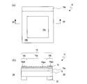
- (A) And (b) is a figure which shows typically the state of the aluminum film provided to an anodic oxidation process in the formation method of the anodic oxidation layer of embodiment by this invention, (a) is a top view, (B) is a cross section taken along line 1B-1B ′ in (a). (A) And (b) is a figure which shows typically the mold 10 for moth eyes which has the porous alumina layer 18 formed by the formation method of the anodic oxidation layer of embodiment by this invention, (a) is a top view , (B) is a cross section taken along line 2B-2B 'in (a). It is typical sectional drawing of the to-be-processed object used by the experiment example.
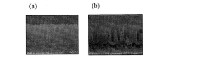
- FIG. (A) is a cross-sectional SEM image of the porous alumina layer 18 of the moth-eye mold 10, wherein (a) is a cross-section of a region 18b corresponding to a region where the low thermal conductive member 22 is provided on the back side of the glass substrate 12, and (b) It is the cross section of the area
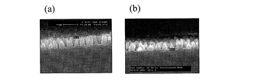
- FIG. (A) And (b) is a figure which shows the cross-sectional SEM image of the antireflection film produced using the type
- FIG. 1 It is a graph which shows the measurement result of the spectral reflectance of the anti-reflective film produced using the type
- (A) to (c) are cross-sectional SEM images of an antireflection film formed using a moth-eye mold having a porous alumina layer formed on a glass substrate, a PET substrate, and a TAC substrate, respectively.
- (A)-(c) is a figure which shows the SEM image of the surface of the aluminum film deposited on the glass substrate, the PET substrate, and the TAC substrate, respectively.
- the inventor of the present invention pays attention to the fact that the structure of the porous alumina layer depends on the temperature at the time of anodic oxidation. By actively utilizing this phenomenon, the fine structure (for example, the depth of the fine recesses) is mutually reduced.
- the inventors have come up with a method for forming a porous alumina layer having different regions in a predetermined pattern. That is, according to the method for forming an anodic oxide layer of the embodiment of the present invention, it is possible to form a porous alumina layer having regions having different fine structures (for example, depths of fine recesses) in a predetermined pattern.
- an embodiment of the present invention will be described by taking as an example a method of forming an anodized layer that can be used as a mold of an antireflection film.
- the method for forming an anodized layer includes a step of preparing an aluminum film formed on a first main surface of a support, and a plurality of fine recesses by anodizing the surface of the aluminum film. Forming a porous alumina layer.
- the anodic oxidation is performed in a state where the low heat conductive member having a predetermined pattern is provided on the second main surface opposite to the first main surface of the support.
- a porous alumina layer in which a region having a fine structure (for example, a depth of a fine concave portion) different from other regions is formed according to the pattern of the low heat conductive member is obtained.
- FIGS. 1 and 2 a method for forming an anodized layer according to an embodiment of the present invention will be described in detail.
- FIGS. 1A and 1B are diagrams schematically showing the state of an aluminum film subjected to an anodizing step in the method for forming an anodized layer according to an embodiment of the present invention, and FIG. Is a plan view, and FIG. 1B is a cross-sectional view taken along line 1B-1B ′ in FIG.
- the aluminum film 16 is subjected to an anodic oxidation step in a state where it is formed on the support 12 of the object to be processed 10a. That is, the aluminum film 16 is formed on the first main surface (front side) of the support 12.
- the support 12 is, for example, a glass substrate or a plastic substrate.
- a low heat conductive member 22 having a predetermined pattern is provided on the second main surface (back side) opposite to the first main surface of the support 12.
- a low thermal conductive member 22 having a frame-like pattern is provided around the rectangular support 12.
- the low heat conductive member 22 may be any member that can slow down the rate at which Joule heat generated during anodization is released into the electrolyte solution, and is made of an insulating material (for example, glass or plastic) in the same manner as the support 12. Is formed.
- an electrode extraction portion 16 e is provided on the upper end of the aluminum film 16. This part is not in contact with the electrolyte and is connected to the positive electrode of the external power source for anodization.
- a method for taking out the electrode it is preferable to adopt the method described in PCT / JP2010 / 000937 by the present applicant.
- a porous alumina layer having a plurality of fine recesses is formed by anodizing the surface of the aluminum film 16 in a state in which the object to be processed 10a is immersed in a predetermined electrolytic solution. At this time, Joule heat is generated as the anodic oxidation proceeds. Joule heat is transmitted from the aluminum film 16 and the formed porous alumina layer to the electrolytic solution and also to the electrolytic solution through the support 12.
- the low thermal conductive member 22 provided on the back side of the support 12 prevents Joule heat generated from the front side of the support 12 from being conducted to the electrolyte on the back side of the support 12 via the support 12. Acts as follows. Accordingly, heat easily accumulates in the region of the support 12 where the low heat conductive member 22 is provided, and as a result, the region of the support 12 where the low heat conductive member 22 is provided has a higher temperature than the other regions. .
- the temperature of the aluminum film 16 (or porous alumina layer) in the region corresponding to the region where the low thermal conductive member 22 of the support 12 is provided is naturally higher than the temperature of the aluminum film 16 in other regions. . Since the structure of the porous alumina layer also depends on the temperature at the time of anodization (temperature of the electrolytic solution), the porous alumina layer having a different structure is formed according to the temperature distribution pattern formed by the low thermal conductive member 22.
- the porous alumina layer is brought into contact with the etching solution by contacting the porous alumina layer with the etching solution.
- Porous suitably used as a moth-eye mold for forming an antireflection film by performing a step of enlarging fine concave portions of a layer and a step of growing fine concave portions of a porous alumina layer by anodizing An alumina layer can be formed.
- the moth-eye mold 10 shown in FIGS. 2A and 2B can be obtained by alternately repeating the anodizing step and the etching step a plurality of times (for example, 5 times: anodizing 5 times and etching 4 times). Obtainable.
- FIG. 2A and 2B are views schematically showing a moth-eye mold 10 having a porous alumina layer 18 formed by the method for forming an anodized layer according to an embodiment of the present invention. ) Is a plan view, and FIG. 2B is a cross-sectional view taken along the line 2B-2B ′ in FIG.
- the moth-eye mold 10 has a porous alumina layer 18 formed by anodizing a part of the surface of the aluminum film 16 as shown in FIG. 2 (b).
- the aluminum layer 16a remains below the porous alumina layer 18 (on the support 12 side).
- the porous alumina layer 18 includes a porous layer having fine concave portions and a barrier layer formed on the lower side (aluminum layer 16a side).
- the porous alumina layer 18 has a fine structure corresponding to the type of electrolyte, applied voltage, and temperature. This fine structure is characterized by the depth and diameter of the fine recesses and the spacing between adjacent fine recesses (or the pitch if the fine recesses are regularly arranged). As described above, even when the temperature of the electrolytic solution is kept constant, the support 12 and the low thermal conductive member 22 form a temperature distribution in the aluminum film 16 and the porous alumina layer 18 where anodization proceeds.
- the layer 18 has, for example, a first recess 18pa and a second recess 18pb having different depths.
- a second recess 18pb deeper than the first recess 18pa formed in the other region 18a is formed in the region 18b corresponding to the region where the low heat conductive member 22 is provided on the back side of the support 12.
- the region 18 b having a fine structure different from that of the other region 18 a of the porous alumina layer 18 can be used as the pattern of the low thermal conductive member 22. Can be formed correspondingly. Therefore, according to the method for forming the anodized layer of the embodiment of the present invention, the region 18b can be formed in an arbitrary pattern only by changing the pattern of the low thermal conductive member 22.
- the predetermined pattern can represent information by forming a pattern including characters, graphics or symbols or a combination thereof.
- the predetermined pattern is caused by the difference in the structure (height) of the fine convex portions, as will be described later by showing an experimental example. It can be visually recognized by the naked eye due to the difference in spectral reflectance in the visible light region. Accordingly, information represented by the predetermined pattern is recognized by a person observing the antireflection film. For example, product management information such as characters representing company names, logos or marks, or numbers or symbols representing manufacturing lot numbers can be represented.
- an aluminum film is formed on a support such as a glass substrate or a plastic substrate. Therefore, if the adhesion between the support and the aluminum film is not sufficient, the anode In the oxidation step and / or etching step, the aluminum film may be peeled off by repeating these steps alternately. Therefore, it is preferable to form an inorganic underlayer and an aluminum-containing buffer layer in this order on the surface of a substrate made of glass or plastic, and then form an aluminum film on the surface of the buffer layer.
- the inorganic underlayer also has a function of preventing alkali metal from eluting from, for example, a glass substrate.
- the inorganic underlayer is preferably a silicon dioxide layer or a titanium oxide layer, and the thickness of the inorganic underlayer is preferably from 100 nm to 200 nm.
- a buffer layer what has the profile whose aluminum content rate is higher in the porous alumina layer side than the inorganic base layer side like the buffer layer described in the international publication 2010/116728 is preferable.
- the thickness of the buffer layer is preferably 100 nm or more and 200 nm or less. For reference purposes, the entire disclosure of WO 2010/116728 is incorporated herein by reference.
- an aluminum film is once formed on the buffer layer, the surface of the aluminum film is naturally oxidized, and then the aluminum film is formed on the surface of the natural oxide film.
- the etching solution may permeate into the gaps between crystal grains constituting the aluminum film, and pinholes may be formed.
- the temperature distribution of the electrolyte is important. That is, when the low heat conductive member is not provided, it is necessary to form a porous alumina layer having a uniform moth-eye structure over the entire surface.
- the temperature distribution in the electrolytic solution near the liquid surface is It was found that a uniform moth-eye structure was formed on the entire surface without being influenced by the rising).
- a glass substrate or a plastic substrate was used as the base material.
- a polyethylene terephthalate (PET) substrate or a triacetyl cellulose (TAC) substrate was used as the plastic substrate.
- the size of the substrate used here was a large substrate of 1 m ⁇ 1.6 m
- the thickness of the glass substrate was 2.8 mm
- the thickness of the PET substrate was 188 ⁇ m
- the thickness of the TAC substrate was 80 ⁇ m.
- the PET substrate and the TAC substrate are film-like, and as such, deformation such as bending of the substrate occurs due to convection of the liquid in the electrolytic solution or the etching solution.
- plastic substrates films
- FIXFILm double-sided fix film
- Fuji Copian a plastic substrate
- a fix film a plastic substrate can be detachably attached to a smooth surface such as a glass substrate without using an adhesive (including an adhesive).
- FIG. 3 shows a schematic cross-sectional view of the object to be processed used in the experimental example.
- the aluminum film 16 was formed.
- the base material 12 s and the inorganic base layer 13 are collectively referred to as a support 12.
- the SiO 2 layer 13 having a thickness of 150 nm is formed on the glass substrate 12s by a sputtering method.
- an aluminum oxide layer 14a having a thickness of 300 nm is formed on the inorganic underlayer 13 by sputtering.
- the sputtering conditions are as follows. G. The degree of vacuum was 1 ⁇ 10 ⁇ 5 Torr, the atmosphere gas was Ar, the degree of vacuum during sputtering was 1 ⁇ 10 ⁇ 3 Torr, and the Al target purity was 99.999%. The purity of the Al target may be 99.99% or more. 1 Torr is 1.33322 ⁇ 10 ⁇ 1 kPa. In the process of forming the aluminum oxide layer 14a, the aluminum concentration is gradually lowered to form the aluminum oxide layer 14a having a higher aluminum content on the porous alumina layer side than on the inorganic underlayer side. In addition, the aluminum oxide layer 14a should just be an insulator with high acid resistance, for example, can use an aluminum nitride layer.
- an aluminum layer 14b having a thickness of 200 nm is formed on the aluminum oxide layer 14a, and the surface thereof is naturally oxidized to form a natural oxide film 14c having a thickness of about 10 nm.
- the aluminum oxide layer 14a, the aluminum layer 14b, and the natural oxide film 14c may be collectively referred to as an aluminum-containing base layer 14.
- An aluminum film 16 having a thickness of 800 nm is formed on the natural oxide film 14c by sputtering.
- porous alumina layer 18 is formed by repeating anodic oxidation and etching on the aluminum film 16.
- Anodization is performed for 37 seconds at an applied voltage of 80 V using 0.025 mol / L (liter) oxalic acid aqueous solution. After washing with pure water, etching was performed for 29 minutes using a 1 mol / L phosphoric acid aqueous solution, followed by washing with water again. This cycle was repeated four times, and finally anodization was performed once again.
- the set temperature of the electrolytic solution was 18 ° C., and anodic oxidation was performed in a state where the upper end of the object to be processed 10a was set at a position deeper than the liquid level of the electrolytic solution by 20 cm or more.
- the surface temperature of the object 10a on the side of the aluminum film 16 was 23 ° C.
- the surface temperature on the aluminum film 16 side of the object to be processed 10a located at a depth of 5 cm from the liquid surface reached about 40 ° C. at the second anodic oxidation, whereas from the liquid surface. It was confirmed that it was almost equal to the liquid temperature at a position deeper than 20 cm.
- the temperature of the etching solution was about 27 ° C. in all four etching steps.
- the to-be-processed object 10a was conveyed to the to-be-processed object 10a (without drying) from the electrolytic bath to the water-washing bath, from the water-washing bath to the etching bath, and from the etching bath to the water-washing bath. .
- it can prevent that the mist of a solvent adheres to the surface of the to-be-processed object 10a. Since various solvents are used during the process, they may not be removed if different types of solvents are deposited.
- 4A and 4B show cross-sectional SEM images of the porous alumina layer 18 of the moth-eye mold 10 (see FIG. 2) obtained as described above.
- 4A shows a cross section of a region 18b of the porous alumina layer 18 corresponding to a region where the low thermal conductive member (acrylic plate) 22 is provided on the back side of the glass substrate 12, and
- FIG. 4B shows the porous alumina layer 18.
- region which has not provided the low heat conductive member (acrylic board) 22 in the back side of the glass substrate 12 is shown.
- the average depth of the pores shown in FIG. 4A (recessed portion 18pb in FIG. 2B) is 510 nm, and the pores shown in FIG. 4B (FIG. 2B) The average depth of the recesses 18pa) was 410 nm. The diameters of the pores were all about 180 nm, and no significant difference was observed.
- FIGS. 5 (a) and 5 (b) show cross-sectional SEM images of the antireflection film produced using the moth-eye mold 10 described above.
- FIGS. 5A and 5B correspond to the regions shown in FIGS. 4A and 4B, respectively.
- the antireflection film was produced as follows.
- An ultraviolet curable resin (thickness 40 ⁇ m) was applied on a TAC film (thickness 75 ⁇ m). Thereafter, the moth-eye mold 10 was pressed so that the ultraviolet curable resin was filled between the moth-eye mold 10 and the surface of the TAC film. In this state, the ultraviolet curable resin was cured by irradiating ultraviolet rays through the TAC film.
- An acrylic resin manufactured by DNP Fine Chemical Co., Ltd. was used as the ultraviolet curable resin.
- the average height of the convex portions shown in FIG. 5A of the antireflection film was about 290 nm, and the average height of the convex portions shown in FIG. 5B was about 200 nm.
- the reason why the height of the convex portion of the antireflection film is smaller than the depth of the concave portion of the moth-eye mold is due to curing shrinkage of the ultraviolet curable resin and insufficient filling of the resin into the pores.
- FIG. 6 shows the measurement results of the spectral reflectance of the antireflection film.
- FIG. 6 shows the measurement results for the region corresponding to the region shown in FIG. 5A (the region to which the region 18b in FIG. 2 is transferred) and the region corresponding to the region shown in FIG. The measurement results for the region 18a to which the region 18a in FIG. 2 is transferred are also shown.
- a spectral colorimeter (CM-2600d) manufactured by Konica Minolta was used for the measurement of the spectral reflectance.
- the reflected light includes not only regular reflected light but also scattered light from the antireflection film, and the reflectance on the vertical axis is larger than the regular reflectance.
- the spectral reflectance in the visible light region is different between the two regions.
- the spectral reflectance of the region where the region 18b of the moth-eye mold 10 is transferred is larger than the spectral reflectance of the region where the region 18a of the moth-eye mold 10 is transferred at around 480 nm.
- the area where the area 18b of the moth-eye mold 10 is transferred appears colored yellow and the area where the area 18a of the moth-eye mold 10 is transferred Looks reddish.
- the reflectance in any region is 0.4% or less, and functions sufficiently as an antireflection film.
- the fine structure of the porous alumina layer such as the depth of the pores, the diameter of the pores, the distance between adjacent pores (center-to-center distance), the degree of regularity of the arrangement of the pores, the type of electrolyte, concentration, temperature, Since it changes depending on the magnitude of the applied voltage, the application time, etc., it may be adjusted as necessary.
- the porous alumina layer 18 of the moth-eye mold 10 for producing an antireflection film has a two-dimensional size (pore diameter) of 10 nm to 500 nm, an adjacent pore interval of 10 nm to 500 nm, and a pore depth.
- the thickness is preferably from 100 nm to 500 nm and having no regularity in the pore distribution.
- the fine structure of the porous alumina layer is affected by the heat dissipation of the workpiece 10a during anodization. Therefore, even if the electrolytic solution and the applied voltage are the same, if the thermal conductivity of the material constituting the support 12 is different, the fine structure of the resulting porous alumina layer is different.
- the anodic oxidation step and the etching step are performed under the same conditions as in the above experimental example.
- the result of forming the porous alumina layer will be described.
- the fine structure of the porous alumina layer to be formed differs depending on the type of base material, that is, the thermal conductivity (heat dissipation) of the base material, depending on the desired fine structure, the type of electrolyte,
- the anodic oxidation conditions such as concentration, temperature, applied voltage, and application time, it is necessary to appropriately select the type of substrate.
- FIGS. 7A to 7C are cross-sectional SEMs of antireflection films obtained by the above-described method using a moth-eye mold having a porous alumina layer formed on a glass substrate, a PET substrate, and a TAC substrate, respectively. It is a figure which shows an image.
- the height of the convex portion of the antireflection film was about 200 nm when a mold having a glass substrate was used, about 230 nm when a PET substrate was used, and about 360 nm when a TAC substrate was used.
- the thermal conductivities of glass, PET, and TAC are 1.0, 0.20 to 0.33, and 0.17 to 0.33 W / m ⁇ K, respectively, near room temperature (25 ° C.). It can be seen that the mold having a substrate having a low thermal conductivity tends to have a higher height of the convex portion of the antireflection film formed using the mold. That is, as the thermal conductivity of the substrate is smaller, Joule heat generated during anodization tends to accumulate on the surface of the substrate and the electrolytic reaction is promoted. As a result, a porous alumina layer having deep pores is formed.
- FIGS. 8A to 8C are views showing SEM images of the surfaces of the aluminum films deposited on the glass substrate, the PET substrate, and the TAC substrate, respectively.
- the conditions for forming the aluminum film are as follows. G. Degree of vacuum: 1 ⁇ 10 ⁇ 5 Torr, atmosphere gas: Ar, degree of vacuum during sputtering: 1 ⁇ 10 ⁇ 3 Torr, Al target purity: 99.999% there were.
- the crystal grains when the glass substrate is used, the crystal grains have a relatively densely aggregated form, and there are some variations, but the crystal grains are almost the same size.
- FIG. 8B when a PET substrate is used, relatively many holes (observed as small black dots) are formed between crystal grains. It can also be seen that the variation in the shape and size of the crystal grains is large and the surface is rough.
- FIG. 8C when the TAC base material is used, an aluminum film having a form close to that of the aluminum film when the glass substrate is used is obtained. When the TAC substrate is used, there are more pores between crystal grains.
- the form of the aluminum film is also considered to affect the fine structure of the porous alumina layer. Therefore, it is preferable to know in advance the influence of the type of substrate on the microstructure of the porous alumina layer in accordance with the desired microstructure.
- the embodiment of the present invention is not limited to this, and the aluminum film formed on various supports. Can be used.
- the shape of the support is not limited to the substrate, and may be a cylinder.
- the material of the support may not have insulating properties, and it is sufficient that at least the surface (first main surface) in contact with the aluminum film has insulating properties.
- the insulating film may be an inorganic insulating film such as an inorganic oxide or an inorganic nitride, or may be an organic insulating film.
- the support is preferably formed of an insulator, and it is preferable to use a support having resistance to the electrolytic solution (and etching solution if necessary).
- a support having a main body of a metal material may be used.
- the present invention is used to form an anodized porous alumina layer used for various applications.
Landscapes
- Chemical & Material Sciences (AREA)
- Engineering & Computer Science (AREA)
- Materials Engineering (AREA)
- Chemical Kinetics & Catalysis (AREA)
- Electrochemistry (AREA)
- Metallurgy (AREA)
- Organic Chemistry (AREA)
- Mechanical Engineering (AREA)
- Physics & Mathematics (AREA)
- Manufacturing & Machinery (AREA)
- General Physics & Mathematics (AREA)
- Optics & Photonics (AREA)
- Surface Treatment Of Optical Elements (AREA)
- Laminated Bodies (AREA)
Abstract
Description
10a 被処理体
12 支持体
16 アルミニウム膜
16e 電極取り出し部
18 ポーラスアルミナ層
22 低熱伝導部材
Claims (6)
- 支持体の第1主面上に形成されたアルミニウム膜を用意する工程であって、前記支持体の前記第1主面とは反対側の第2主面上には所定のパターンを有する低熱伝導部材が設けられている、工程(a)と、前記アルミニウム膜の表面を陽極酸化することによって複数の微細な凹部を有するポーラスアルミナ層を形成する工程(b)と
を包含する陽極酸化層の形成方法。 - 前記工程(b)の後に、前記ポーラスアルミナ層を、エッチング液に接触させることによって、前記ポーラスアルミナ層の前記複数の微細な凹部を拡大させる工程(c)と、
前記工程(c)の後に、さらに陽極酸化することによって、前記複数の微細な凹部を成長させる工程(d)と
を包含する、請求項1に記載の陽極酸化層の形成方法。 - 前記所定のパターンは情報を表している、請求項1または2に記載の陽極酸化層の形成方法。
- 前記工程(a)は、
基材と前記基材の表面に形成された無機下地層とを有し、前記無機下地層の表面が前記第1主面である前記支持体を用意する工程と、
前記無機下地層の上にアルミニウム層を形成する工程と、
前記アルミニウム層の表面に自然酸化膜を形成する工程と、
前記自然酸化膜の表面に前記アルミニウム膜を形成する工程を包含する、請求項1から3のいずれかに記載の陽極酸化層の形成方法。 - 請求項1から4のいずれかに記載の陽極酸化層の形成方法で、表面の法線方向から見たときの2次元的な大きさが10nm以上500nm未満の複数の微細な凹部を有するポーラスアルミナ層を形成する工程を包含する、反転されたモスアイ構造を表面に有する型の製造方法。
- 請求項5に記載の製造方法で製造された型と、被加工物とを用意する工程と、
前記型と前記被加工物の表面との間に紫外線硬化樹脂を付与した状態で、前記型を介して前記紫外線硬化樹脂に紫外線を照射することによって前記紫外線硬化樹脂を硬化する工程と
を包含する、反射防止膜の製造方法。
Priority Applications (2)
| Application Number | Priority Date | Filing Date | Title |
|---|---|---|---|
| US13/583,399 US9108351B2 (en) | 2010-03-09 | 2011-03-08 | Method for forming anodized layer, method for producing mold and method for producing antireflective film |
| CN201180012799.0A CN102791909B (zh) | 2010-03-09 | 2011-03-08 | 阳极氧化层的形成方法、模具的制造方法以及防反射膜的制造方法 |
Applications Claiming Priority (2)
| Application Number | Priority Date | Filing Date | Title |
|---|---|---|---|
| JP2010052304 | 2010-03-09 | ||
| JP2010-052304 | 2010-03-09 |
Publications (1)
| Publication Number | Publication Date |
|---|---|
| WO2011111697A1 true WO2011111697A1 (ja) | 2011-09-15 |
Family
ID=44563498
Family Applications (1)
| Application Number | Title | Priority Date | Filing Date |
|---|---|---|---|
| PCT/JP2011/055364 Ceased WO2011111697A1 (ja) | 2010-03-09 | 2011-03-08 | 陽極酸化層の形成方法、型の製造方法および反射防止膜の製造方法 |
Country Status (3)
| Country | Link |
|---|---|
| US (1) | US9108351B2 (ja) |
| CN (1) | CN102791909B (ja) |
| WO (1) | WO2011111697A1 (ja) |
Cited By (8)
| Publication number | Priority date | Publication date | Assignee | Title |
|---|---|---|---|---|
| JP2013112892A (ja) * | 2011-12-01 | 2013-06-10 | Dnp Fine Chemicals Co Ltd | ナノ構造体作製用型体の製造方法、製造装置、ナノ構造体作製用型体及びナノ構造体 |
| JP2013250203A (ja) * | 2012-06-01 | 2013-12-12 | Denso Corp | 液体成分センサ |
| WO2013191091A1 (ja) * | 2012-06-22 | 2013-12-27 | シャープ株式会社 | 反射防止構造体、転写用型、これらの製造方法、及び、表示装置 |
| JP2014107155A (ja) * | 2012-11-28 | 2014-06-09 | Minebea Co Ltd | 面状照明装置 |
| WO2014104308A1 (ja) * | 2012-12-28 | 2014-07-03 | 三菱レイヨン株式会社 | 光学物品、光学物品の製造に用いられる型及び型の製造方法 |
| WO2014162374A1 (ja) * | 2013-04-02 | 2014-10-09 | パナソニック株式会社 | 光学部材および光学装置 |
| US9128220B2 (en) | 2010-11-29 | 2015-09-08 | Sharp Kabushiki Kaisha | Light guide body with continuously variable refractive index, and devices using such body |
| WO2016027827A1 (ja) * | 2014-08-21 | 2016-02-25 | シャープ株式会社 | 型および型の製造方法 |
Families Citing this family (6)
| Publication number | Priority date | Publication date | Assignee | Title |
|---|---|---|---|---|
| JP5323257B2 (ja) | 2010-04-28 | 2013-10-23 | シャープ株式会社 | バックライトユニットおよび液晶表示装置 |
| CN104166173B (zh) * | 2013-05-17 | 2016-08-24 | 群创光电股份有限公司 | 抗反射基板及包含其的显示设备 |
| US9457493B2 (en) * | 2013-08-14 | 2016-10-04 | Mitsubishi Rayon Co., Ltd. | Method for producing cylindrical nanoimprinting mold and method for producing nanoimprinting reproduction mold |
| JP7452143B2 (ja) * | 2020-03-19 | 2024-03-19 | セイコーエプソン株式会社 | マルチレンズアレイ、光源装置およびプロジェクター |
| EP4143615A1 (en) | 2020-04-27 | 2023-03-08 | Glint Photonics, Inc. | Method for producing optical article with anti-reflective surface, and optical article with anti-reflective surface |
| CN111907090A (zh) * | 2020-07-30 | 2020-11-10 | 中国空气动力研究与发展中心低速空气动力研究所 | 一种热固性树脂基复合材料表面防冰阵列结构的成型方法 |
Citations (2)
| Publication number | Priority date | Publication date | Assignee | Title |
|---|---|---|---|---|
| JP2003531962A (ja) * | 2000-04-28 | 2003-10-28 | アルコーブ サーフィシーズ ゲーエムベーハー | 型押し具、これを製造する方法、加工物の表面を構築する方法、及び陽極酸化表面層の使用 |
| JP2005156695A (ja) * | 2003-11-21 | 2005-06-16 | Kanagawa Acad Of Sci & Technol | 反射防止膜及びその製造方法、並びに反射防止膜作製用スタンパ及びその製造方法 |
Family Cites Families (14)
| Publication number | Priority date | Publication date | Assignee | Title |
|---|---|---|---|---|
| US3864217A (en) * | 1974-01-21 | 1975-02-04 | Nippon Electric Co | Method of fabricating a semiconductor device |
| JPH08144097A (ja) | 1994-11-21 | 1996-06-04 | Ricoh Co Ltd | 陽極酸化処理方法 |
| DE19708776C1 (de) | 1997-03-04 | 1998-06-18 | Fraunhofer Ges Forschung | Entspiegelungsschicht sowie Verfahren zur Herstellung derselben |
| JPH10324998A (ja) | 1997-05-26 | 1998-12-08 | Ykk Corp | アルミニウム形材の陽極酸化皮膜生成時における酸化皮膜厚制御方法 |
| US7066234B2 (en) | 2001-04-25 | 2006-06-27 | Alcove Surfaces Gmbh | Stamping tool, casting mold and methods for structuring a surface of a work piece |
| US20070235342A1 (en) * | 2004-10-01 | 2007-10-11 | Canon Kabushiki Kaisha | Method for manufacturing nanostructure |
| KR100893251B1 (ko) | 2004-12-03 | 2009-04-17 | 샤프 가부시키가이샤 | 반사 방지재, 광학 소자, 및 표시 장치 및 스탬퍼의 제조방법 및 스탬퍼를 이용한 반사 방지재의 제조 방법 |
| JP4813925B2 (ja) * | 2006-02-28 | 2011-11-09 | 富士フイルム株式会社 | 微細構造体の製造方法および微細構造体 |
| US7655127B2 (en) * | 2006-11-27 | 2010-02-02 | 3M Innovative Properties Company | Method of fabricating thin film transistor |
| JP4870544B2 (ja) * | 2006-12-25 | 2012-02-08 | 富士フイルム株式会社 | 微細構造体の製造方法および微細構造体 |
| TWI504500B (zh) * | 2007-10-25 | 2015-10-21 | 三菱麗陽股份有限公司 | 壓模及其製造方法、成形體的製造方法以及壓模的鋁原型 |
| CN101403117A (zh) * | 2008-11-07 | 2009-04-08 | 长沙湘计海盾科技有限公司 | 一种铝或铝合金制品表面的复合氧化工艺 |
| WO2010095415A1 (ja) | 2009-02-17 | 2010-08-26 | シャープ株式会社 | 型の製造方法およびそれに用いられる電極構造 |
| RU2482221C1 (ru) | 2009-04-09 | 2013-05-20 | Шарп Кабусики Кайся | Форма и способ ее изготовления |
-
2011
- 2011-03-08 US US13/583,399 patent/US9108351B2/en active Active
- 2011-03-08 CN CN201180012799.0A patent/CN102791909B/zh not_active Expired - Fee Related
- 2011-03-08 WO PCT/JP2011/055364 patent/WO2011111697A1/ja not_active Ceased
Patent Citations (2)
| Publication number | Priority date | Publication date | Assignee | Title |
|---|---|---|---|---|
| JP2003531962A (ja) * | 2000-04-28 | 2003-10-28 | アルコーブ サーフィシーズ ゲーエムベーハー | 型押し具、これを製造する方法、加工物の表面を構築する方法、及び陽極酸化表面層の使用 |
| JP2005156695A (ja) * | 2003-11-21 | 2005-06-16 | Kanagawa Acad Of Sci & Technol | 反射防止膜及びその製造方法、並びに反射防止膜作製用スタンパ及びその製造方法 |
Cited By (14)
| Publication number | Priority date | Publication date | Assignee | Title |
|---|---|---|---|---|
| US9128220B2 (en) | 2010-11-29 | 2015-09-08 | Sharp Kabushiki Kaisha | Light guide body with continuously variable refractive index, and devices using such body |
| JP2013112892A (ja) * | 2011-12-01 | 2013-06-10 | Dnp Fine Chemicals Co Ltd | ナノ構造体作製用型体の製造方法、製造装置、ナノ構造体作製用型体及びナノ構造体 |
| JP2013250203A (ja) * | 2012-06-01 | 2013-12-12 | Denso Corp | 液体成分センサ |
| JPWO2013191091A1 (ja) * | 2012-06-22 | 2016-05-26 | シャープ株式会社 | 反射防止構造体、転写用型、これらの製造方法、及び、表示装置 |
| CN104395784A (zh) * | 2012-06-22 | 2015-03-04 | 夏普株式会社 | 防反射结构体、转印用模具、它们的制造方法和显示装置 |
| WO2013191091A1 (ja) * | 2012-06-22 | 2013-12-27 | シャープ株式会社 | 反射防止構造体、転写用型、これらの製造方法、及び、表示装置 |
| JP2014107155A (ja) * | 2012-11-28 | 2014-06-09 | Minebea Co Ltd | 面状照明装置 |
| WO2014104308A1 (ja) * | 2012-12-28 | 2014-07-03 | 三菱レイヨン株式会社 | 光学物品、光学物品の製造に用いられる型及び型の製造方法 |
| US9523796B2 (en) | 2012-12-28 | 2016-12-20 | Mitsubishi Rayon Co., Ltd. | Optical article, mold used in production of optical article, and mold production method |
| JPWO2014104308A1 (ja) * | 2012-12-28 | 2017-01-19 | 三菱レイヨン株式会社 | 光学物品、光学物品の製造に用いられる型及び型の製造方法 |
| WO2014162374A1 (ja) * | 2013-04-02 | 2014-10-09 | パナソニック株式会社 | 光学部材および光学装置 |
| JPWO2014162374A1 (ja) * | 2013-04-02 | 2017-02-16 | パナソニックIpマネジメント株式会社 | 光学部材および光学装置 |
| WO2016027827A1 (ja) * | 2014-08-21 | 2016-02-25 | シャープ株式会社 | 型および型の製造方法 |
| JPWO2016027827A1 (ja) * | 2014-08-21 | 2017-07-06 | シャープ株式会社 | 型 |
Also Published As
| Publication number | Publication date |
|---|---|
| CN102791909A (zh) | 2012-11-21 |
| US9108351B2 (en) | 2015-08-18 |
| CN102791909B (zh) | 2015-05-20 |
| US20120325670A1 (en) | 2012-12-27 |
Similar Documents
| Publication | Publication Date | Title |
|---|---|---|
| WO2011111697A1 (ja) | 陽極酸化層の形成方法、型の製造方法および反射防止膜の製造方法 | |
| US8758589B2 (en) | Antireflection film, optical element comprising antireflection film, stamper, process for producing stamper, and process for producing antireflection film | |
| TWI484071B (zh) | 陽極氧化層之形成方法及模具之製造方法 | |
| JP4916597B2 (ja) | 型および型の製造方法ならびに反射防止膜 | |
| TWI602954B (zh) | 陽極氧化多孔氧化鋁的製造方法、模具以及表面具有微細凹凸結構的成形體 | |
| US9469056B2 (en) | Mold, mold manufacturing method and method for manufacturing anti-reflection film using the mold | |
| JP4531131B1 (ja) | 型の製造方法および型を用いた反射防止膜の製造方法 | |
| TWI457589B (zh) | 蛾眼用模與蛾眼用模及蛾眼構造之製作方法 | |
| JP5506804B2 (ja) | 陽極酸化層の形成方法、型の製造方法、反射防止膜の製造方法、型、および反射防止膜 | |
| TWI465759B (zh) | 模具及模具之製造方法 | |
| WO2011043464A1 (ja) | 型および型の製造方法ならびに反射防止膜 | |
| JP5940662B2 (ja) | 反射防止フィルムの製造方法 | |
| Kikuchi et al. | Fabrication of a meniscus microlens array made of anodic alumina by laser irradiation and electrochemical techniques | |
| US8641884B2 (en) | Mold manufacturing method and electrode structure for use therein | |
| US9821494B2 (en) | Mold release treatment method and method for producing anti-reflective film | |
| JPWO2016084745A1 (ja) | 型および型の製造方法ならびに反射防止膜 | |
| JPWO2014021039A1 (ja) | 型の製造方法 |
Legal Events
| Date | Code | Title | Description |
|---|---|---|---|
| WWE | Wipo information: entry into national phase |
Ref document number: 201180012799.0 Country of ref document: CN |
|
| 121 | Ep: the epo has been informed by wipo that ep was designated in this application |
Ref document number: 11753355 Country of ref document: EP Kind code of ref document: A1 |
|
| WWE | Wipo information: entry into national phase |
Ref document number: 13583399 Country of ref document: US |
|
| NENP | Non-entry into the national phase |
Ref country code: DE |
|
| 122 | Ep: pct application non-entry in european phase |
Ref document number: 11753355 Country of ref document: EP Kind code of ref document: A1 |
|
| NENP | Non-entry into the national phase |
Ref country code: JP |