WO2011111152A1 - 導電性粒子、異方性導電材料及び接続構造体 - Google Patents
導電性粒子、異方性導電材料及び接続構造体 Download PDFInfo
- Publication number
- WO2011111152A1 WO2011111152A1 PCT/JP2010/053786 JP2010053786W WO2011111152A1 WO 2011111152 A1 WO2011111152 A1 WO 2011111152A1 JP 2010053786 W JP2010053786 W JP 2010053786W WO 2011111152 A1 WO2011111152 A1 WO 2011111152A1
- Authority
- WO
- WIPO (PCT)
- Prior art keywords
- palladium
- nickel
- particles
- layer
- conductive particles
- Prior art date
- Legal status (The legal status is an assumption and is not a legal conclusion. Google has not performed a legal analysis and makes no representation as to the accuracy of the status listed.)
- Ceased
Links
Images


Classifications
-
- H—ELECTRICITY
- H01—ELECTRIC ELEMENTS
- H01R—ELECTRICALLY-CONDUCTIVE CONNECTIONS; STRUCTURAL ASSOCIATIONS OF A PLURALITY OF MUTUALLY-INSULATED ELECTRICAL CONNECTING ELEMENTS; COUPLING DEVICES; CURRENT COLLECTORS
- H01R4/00—Electrically-conductive connections between two or more conductive members in direct contact, i.e. touching one another; Means for effecting or maintaining such contact; Electrically-conductive connections having two or more spaced connecting locations for conductors and using contact members penetrating insulation
- H01R4/04—Electrically-conductive connections between two or more conductive members in direct contact, i.e. touching one another; Means for effecting or maintaining such contact; Electrically-conductive connections having two or more spaced connecting locations for conductors and using contact members penetrating insulation using electrically conductive adhesives
-
- H—ELECTRICITY
- H01—ELECTRIC ELEMENTS
- H01B—CABLES; CONDUCTORS; INSULATORS; SELECTION OF MATERIALS FOR THEIR CONDUCTIVE, INSULATING OR DIELECTRIC PROPERTIES
- H01B1/00—Conductors or conductive bodies characterised by the conductive materials; Selection of materials as conductors
- H01B1/02—Conductors or conductive bodies characterised by the conductive materials; Selection of materials as conductors mainly consisting of metals or alloys
-
- H—ELECTRICITY
- H01—ELECTRIC ELEMENTS
- H01B—CABLES; CONDUCTORS; INSULATORS; SELECTION OF MATERIALS FOR THEIR CONDUCTIVE, INSULATING OR DIELECTRIC PROPERTIES
- H01B1/00—Conductors or conductive bodies characterised by the conductive materials; Selection of materials as conductors
- H01B1/20—Conductive material dispersed in non-conductive organic material
- H01B1/22—Conductive material dispersed in non-conductive organic material the conductive material comprising metals or alloys
-
- H—ELECTRICITY
- H05—ELECTRIC TECHNIQUES NOT OTHERWISE PROVIDED FOR
- H05K—PRINTED CIRCUITS; CASINGS OR CONSTRUCTIONAL DETAILS OF ELECTRIC APPARATUS; MANUFACTURE OF ASSEMBLAGES OF ELECTRICAL COMPONENTS
- H05K3/00—Apparatus or processes for manufacturing printed circuits
- H05K3/30—Assembling printed circuits with electric components, e.g. with resistors
- H05K3/32—Assembling printed circuits with electric components, e.g. with resistors electrically connecting electric components or wires to printed circuits
- H05K3/321—Assembling printed circuits with electric components, e.g. with resistors electrically connecting electric components or wires to printed circuits by conductive adhesives
- H05K3/323—Assembling printed circuits with electric components, e.g. with resistors electrically connecting electric components or wires to printed circuits by conductive adhesives by applying an anisotropic conductive adhesive layer over an array of pads
-
- H—ELECTRICITY
- H05—ELECTRIC TECHNIQUES NOT OTHERWISE PROVIDED FOR
- H05K—PRINTED CIRCUITS; CASINGS OR CONSTRUCTIONAL DETAILS OF ELECTRIC APPARATUS; MANUFACTURE OF ASSEMBLAGES OF ELECTRICAL COMPONENTS
- H05K2201/00—Indexing scheme relating to printed circuits covered by H05K1/00
- H05K2201/02—Fillers; Particles; Fibers; Reinforcement materials
- H05K2201/0203—Fillers and particles
- H05K2201/0206—Materials
- H05K2201/0212—Resin particles
-
- H—ELECTRICITY
- H05—ELECTRIC TECHNIQUES NOT OTHERWISE PROVIDED FOR
- H05K—PRINTED CIRCUITS; CASINGS OR CONSTRUCTIONAL DETAILS OF ELECTRIC APPARATUS; MANUFACTURE OF ASSEMBLAGES OF ELECTRICAL COMPONENTS
- H05K2201/00—Indexing scheme relating to printed circuits covered by H05K1/00
- H05K2201/02—Fillers; Particles; Fibers; Reinforcement materials
- H05K2201/0203—Fillers and particles
- H05K2201/0206—Materials
- H05K2201/0218—Composite particles, i.e. first metal coated with second metal
-
- H—ELECTRICITY
- H05—ELECTRIC TECHNIQUES NOT OTHERWISE PROVIDED FOR
- H05K—PRINTED CIRCUITS; CASINGS OR CONSTRUCTIONAL DETAILS OF ELECTRIC APPARATUS; MANUFACTURE OF ASSEMBLAGES OF ELECTRICAL COMPONENTS
- H05K2201/00—Indexing scheme relating to printed circuits covered by H05K1/00
- H05K2201/02—Fillers; Particles; Fibers; Reinforcement materials
- H05K2201/0203—Fillers and particles
- H05K2201/0206—Materials
- H05K2201/0221—Insulating particles having an electrically conductive coating
-
- H—ELECTRICITY
- H10—SEMICONDUCTOR DEVICES; ELECTRIC SOLID-STATE DEVICES NOT OTHERWISE PROVIDED FOR
- H10W—GENERIC PACKAGES, INTERCONNECTIONS, CONNECTORS OR OTHER CONSTRUCTIONAL DETAILS OF DEVICES COVERED BY CLASS H10
- H10W72/00—Interconnections or connectors in packages
- H10W72/071—Connecting or disconnecting
- H10W72/074—Connecting or disconnecting of anisotropic conductive adhesives
-
- H—ELECTRICITY
- H10—SEMICONDUCTOR DEVICES; ELECTRIC SOLID-STATE DEVICES NOT OTHERWISE PROVIDED FOR
- H10W—GENERIC PACKAGES, INTERCONNECTIONS, CONNECTORS OR OTHER CONSTRUCTIONAL DETAILS OF DEVICES COVERED BY CLASS H10
- H10W72/00—Interconnections or connectors in packages
- H10W72/30—Die-attach connectors
- H10W72/321—Structures or relative sizes of die-attach connectors
- H10W72/325—Die-attach connectors having a filler embedded in a matrix
-
- H—ELECTRICITY
- H10—SEMICONDUCTOR DEVICES; ELECTRIC SOLID-STATE DEVICES NOT OTHERWISE PROVIDED FOR
- H10W—GENERIC PACKAGES, INTERCONNECTIONS, CONNECTORS OR OTHER CONSTRUCTIONAL DETAILS OF DEVICES COVERED BY CLASS H10
- H10W72/00—Interconnections or connectors in packages
- H10W72/30—Die-attach connectors
- H10W72/351—Materials of die-attach connectors
-
- H—ELECTRICITY
- H10—SEMICONDUCTOR DEVICES; ELECTRIC SOLID-STATE DEVICES NOT OTHERWISE PROVIDED FOR
- H10W—GENERIC PACKAGES, INTERCONNECTIONS, CONNECTORS OR OTHER CONSTRUCTIONAL DETAILS OF DEVICES COVERED BY CLASS H10
- H10W72/00—Interconnections or connectors in packages
- H10W72/30—Die-attach connectors
- H10W72/351—Materials of die-attach connectors
- H10W72/352—Materials of die-attach connectors comprising metals or metalloids, e.g. solders
-
- H—ELECTRICITY
- H10—SEMICONDUCTOR DEVICES; ELECTRIC SOLID-STATE DEVICES NOT OTHERWISE PROVIDED FOR
- H10W—GENERIC PACKAGES, INTERCONNECTIONS, CONNECTORS OR OTHER CONSTRUCTIONAL DETAILS OF DEVICES COVERED BY CLASS H10
- H10W72/00—Interconnections or connectors in packages
- H10W72/30—Die-attach connectors
- H10W72/351—Materials of die-attach connectors
- H10W72/353—Materials of die-attach connectors not comprising solid metals or solid metalloids, e.g. ceramics
- H10W72/354—Materials of die-attach connectors not comprising solid metals or solid metalloids, e.g. ceramics comprising polymers
-
- H—ELECTRICITY
- H10—SEMICONDUCTOR DEVICES; ELECTRIC SOLID-STATE DEVICES NOT OTHERWISE PROVIDED FOR
- H10W—GENERIC PACKAGES, INTERCONNECTIONS, CONNECTORS OR OTHER CONSTRUCTIONAL DETAILS OF DEVICES COVERED BY CLASS H10
- H10W74/00—Encapsulations, e.g. protective coatings
- H10W74/10—Encapsulations, e.g. protective coatings characterised by their shape or disposition
- H10W74/15—Encapsulations, e.g. protective coatings characterised by their shape or disposition on active surfaces of flip-chip devices, e.g. underfills
-
- H—ELECTRICITY
- H10—SEMICONDUCTOR DEVICES; ELECTRIC SOLID-STATE DEVICES NOT OTHERWISE PROVIDED FOR
- H10W—GENERIC PACKAGES, INTERCONNECTIONS, CONNECTORS OR OTHER CONSTRUCTIONAL DETAILS OF DEVICES COVERED BY CLASS H10
- H10W90/00—Package configurations
- H10W90/701—Package configurations characterised by the relative positions of pads or connectors relative to package parts
- H10W90/721—Package configurations characterised by the relative positions of pads or connectors relative to package parts of bump connectors
- H10W90/724—Package configurations characterised by the relative positions of pads or connectors relative to package parts of bump connectors between a chip and a stacked insulating package substrate, interposer or RDL
-
- H—ELECTRICITY
- H10—SEMICONDUCTOR DEVICES; ELECTRIC SOLID-STATE DEVICES NOT OTHERWISE PROVIDED FOR
- H10W—GENERIC PACKAGES, INTERCONNECTIONS, CONNECTORS OR OTHER CONSTRUCTIONAL DETAILS OF DEVICES COVERED BY CLASS H10
- H10W90/00—Package configurations
- H10W90/701—Package configurations characterised by the relative positions of pads or connectors relative to package parts
- H10W90/731—Package configurations characterised by the relative positions of pads or connectors relative to package parts of die-attach connectors
- H10W90/734—Package configurations characterised by the relative positions of pads or connectors relative to package parts of die-attach connectors between a chip and a stacked insulating package substrate, interposer or RDL
Definitions
- the present invention relates to conductive particles that can be used for connection between electrodes, and more specifically, conductive particles that can improve connection reliability between electrodes when used for connection between electrodes, and the conductive property.
- the present invention relates to an anisotropic conductive material using particles and a connection structure.
- Anisotropic conductive materials such as anisotropic conductive paste, anisotropic conductive ink, anisotropic conductive adhesive, anisotropic conductive film, or anisotropic conductive sheet are widely known.
- anisotropic conductive materials conductive particles are dispersed in paste, ink, or resin.
- the anisotropic conductive material is used for connection between an IC chip and a flexible printed circuit board, connection between an IC chip and a circuit board having an ITO electrode, and the like.
- connection between an IC chip and a circuit board having an ITO electrode and the like.
- these electrodes can be connected by heating and pressurizing.
- Patent Document 1 discloses base material particles, a nickel layer formed on the surface of the base material particle, and formed on the surface of the nickel layer. Disclosed is a conductive particle comprising a modified palladium layer.
- connection structure is formed using the conductive particles described in Patent Document 1 for connection between the electrodes, the connection resistance between the electrodes becomes high when the connection structure is exposed to high temperature and high humidity. Sometimes.
- An object of the present invention is to form a connection structure by connecting electrodes, and even when the connection structure is exposed to high temperature and high humidity, the conductive particles that do not easily increase the connection resistance between the electrodes, and the An anisotropic conductive material using a conductive particle and a connection structure are provided.
- base particles there are provided base particles, a nickel layer formed on the surface of the base particles, and a palladium layer formed on the surface of the nickel layer.
- conductive particles having a palladium content of 5 to 15% by weight and a palladium content of the palladium layer of 96% by weight or more.
- the conductive particles have protrusions on the surface. In another specific aspect of the present invention, the conductive particles have protrusions on the outer surface of the palladium layer.
- an insulating resin attached to the surface of the palladium layer is further provided.
- the insulating resin is an insulating resin particle.
- the anisotropic conductive material according to the present invention includes conductive particles configured according to the present invention and a binder resin.
- connection structure includes a first connection target member, a second connection target member, and a connection part that electrically connects the first and second connection target members.
- the connecting portion is made of the conductive particles of the present invention or an anisotropic conductive material containing the conductive particles and a binder resin.
- the conductive particles according to the present invention a nickel layer and a palladium layer are formed in this order on the surface of the base particle, the phosphorus content of the nickel layer is in the range of 5 to 15% by weight, and Since the palladium content in the palladium layer is 96% by weight or more, it prevents the connection resistance from increasing when a connection structure using conductive particles for connection between electrodes is exposed to high temperature and high humidity. it can. Therefore, the connection reliability of the connection structure can be improved.
- FIG. 1 is a cross-sectional view showing conductive particles according to an embodiment of the present invention.
- FIG. 2 is a cross-sectional view showing conductive particles according to another embodiment of the present invention.
- FIG. 3 is a front sectional view schematically showing a connection structure using conductive particles according to an embodiment of the present invention.
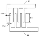
- FIG. 4 is a plan view for explaining the shape of the comb-shaped electrode copper pattern on the substrate used in the evaluation of the insulation resistance of the example and the comparative example.
- FIG. 1 is a cross-sectional view showing conductive particles according to an embodiment of the present invention.
- the conductive particles 1 include a base particle 2, a nickel layer 3 formed on the surface 2 a of the base particle 2, and a palladium layer 4 formed on the surface 3 a of the nickel layer 3. With.
- the conductive particles 1 may further include an insulating resin attached to the surface 4 a of the palladium layer 4.
- FIG. 2 is a cross-sectional view showing conductive particles according to another embodiment of the present invention.
- the conductive particles 21 include base material particles 2, a nickel layer 22 formed on the surface 2 a of the base material particle 2, and a palladium layer 23 formed on the surface 22 a of the nickel layer 22.
- the nickel layer 22 and the palladium layer 23 are metal layers.
- the conductive particle 21 includes a plurality of core substances 24 on the surface 2 a of the base particle 2.
- the nickel layer 22 and the palladium layer 23 that are metal layers cover the core substance 24.
- the conductive particles 21 have a plurality of protrusions 25 on the surface 21a.
- the conductive particle 21 has a plurality of protrusions 25 on the outer surface 23 a of the palladium layer 23.
- the protrusion 25 is formed on the surface 23a of the palladium layer 23 outside the metal layer.
- a surface 23 a of the palladium layer 23 is raised by the core material 24, and a protrusion 25 is formed.
- the conductive particles 21 include an insulating resin 26 attached to the surface 23 a of the palladium layer 23.
- the surface of the palladium layer 23 is covered with an insulating resin 26.
- the insulating resin 26 is insulating resin particles.
- the conductive particles may include an insulating resin 26 that covers the surface 23a of the palladium layer 23.
- the insulating resin 26 is not necessarily provided.
- Examples of the base particle 2 include resin particles, inorganic particles, organic-inorganic hybrid particles, and metal particles.
- Examples of the resin for forming the resin particles include divinylbenzene resin, styrene resin, acrylic resin, urea resin, imide resin, phenol resin, polyester resin, and vinyl chloride resin.
- Examples of the inorganic material for forming the inorganic particles include silica or carbon black.
- Examples of the organic / inorganic hybrid particles include organic / inorganic hybrid particles formed of a crosslinked alkoxysilyl polymer and an acrylic resin.
- Examples of the metal for forming the metal particles include silver, copper, nickel, silicon, gold, and titanium.
- the average particle diameter of the base particle 2 is preferably in the range of 1 to 100 ⁇ m.
- the average particle diameter of the substrate particles is smaller than 1 ⁇ m, the connection reliability between the electrodes may be lowered.
- the average particle diameter of the substrate particles is larger than 100 ⁇ m, the distance between the electrodes may be too large.
- the content of phosphorus in the nickel layers 3 and 22 formed on the surface 2a of the base particle 2 is in the range of 5 to 15% by weight.
- the connection resistance increases when the connection structure using the conductive particles for connection between the electrodes is exposed to high temperature and high humidity.
- the phosphorus content exceeds 15% by weight, the initial connection resistance of the connection structure using the conductive particles for connection between the electrodes becomes high.
- the content of phosphorus in the nickel layers 3 and 22 is 5 to 15% by weight, it becomes easy to obtain fine nickel crystals, and it becomes easy to obtain fine palladium crystals by epitaxial growth of palladium plating. For this reason, the connection reliability of the connection structure under high temperature and high humidity can be improved.
- the phosphorus content in the nickel layers 3 and 22 is preferably in the range of 10 to 15% by weight.
- the content of phosphorus in the nickel layers 3 and 22 is in the range of 10 to 15% by weight, the connection reliability of the connection structure under high temperature and high humidity can be further improved.
- a method of bringing the phosphorus content of the nickel layers 3 and 22 into the above range for example, a method of controlling the pH of a nickel plating solution when forming a nickel layer by electroless nickel plating, or electroless nickel plating
- a method of controlling the concentration of the phosphorus-containing reducing agent when forming the nickel layer by the method described above for example, a method of controlling the concentration of the phosphorus-containing reducing agent when forming the nickel layer by the method described above.
- the method for measuring the phosphorus content of the nickel layer is not particularly limited.
- a thin film section of the obtained conductive particles is prepared using a focused ion beam, and a transmission electron microscope FE-TEM (Japan)
- EDS energy dispersive X-ray analyzer
- the palladium content of the palladium layers 4 and 23 formed on the surfaces 3a and 22a of the nickel layers 3 and 22 is 96% by weight or more.
- the palladium content is preferably 98% by weight or more.
- Examples of a method for making the palladium content of the palladium layers 4 and 23 96% by weight or more include a method of controlling the pH of the palladium plating solution when forming a palladium layer by electroless palladium plating, or electroless palladium.
- a method of controlling the concentration of the reducing agent when forming the palladium layer by plating may be used.
- the method for measuring the palladium content in the palladium layer is not particularly limited.
- a thin film slice of the obtained conductive particles is prepared using a focused ion beam, and a transmission electron microscope FE-TEM (Japan)
- EDS energy dispersive X-ray analyzer
- the total thickness of the metal layers of the nickel layers 3 and 22 and the palladium layers 4 and 23 is preferably in the range of 5 to 500 nm, and more preferably in the range of 10 to 400 nm.
- the thickness of the metal layer is less than 5 nm, the conductivity of the conductive particles may be insufficient.
- the thickness of the metal layer exceeds 500 nm, the difference in coefficient of thermal expansion between the base particle and the metal layer becomes large, and the metal layer may easily peel from the base particle.
- Examples of the method of forming the nickel layers 3 and 22 on the surface 2a of the base particle 2 include a method of forming a nickel layer by electroless plating or a method of forming a nickel layer by electroplating.
- examples of the method of forming the palladium layers 4 and 23 on the surfaces 3a and 22a of the nickel layers 3 and 22 include a method of forming a palladium layer by electroless plating or a method of forming a palladium layer by electroplating.
- the conductive particles preferably have protrusions on the surface.
- the conductive particles preferably have protrusions on the surface of the metal layer, and further preferably have protrusions on the surfaces 4a and 23a of the palladium layers 4 and 23.
- the conductive particles preferably have a plurality of protrusions on the surface.
- the conductive particles preferably have a plurality of protrusions on the surface of the metal layer, and more preferably have a plurality of protrusions on the surfaces 4 a and 23 a of the palladium layers 4 and 23. In these cases, since the resin between the conductive particles and the electrodes can be effectively eliminated, the connection reliability of the connection structure using the conductive particles for the connection between the electrodes can be improved.
- a method of forming protrusions on the surface of the conductive particles a method of forming a metal layer by electroless plating after attaching a core substance to the surface of the base particles, or by electroless plating on the surface of the base particles Examples include a method of forming a metal layer by electroless plating after a core layer is adhered after forming the metal layer.
- a method of attaching the core substance to the surface of the base particle for example, a conductive substance that becomes the core substance is added to the dispersion of the base particle, and the core substance is applied to the surface of the base particle, for example, a fan.
- a method of accumulating and adhering the core substance on the surface of the base particle in the dispersion is preferable because the amount of the core substance to be attached is easy to control.
- Examples of the conductive substance constituting the core substance include metals, metal oxides, conductive nonmetals such as graphite, and conductive polymers.
- Examples of the conductive polymer include polyacetylene. Among them, metal is preferable because conductivity can be increased.
- the metal examples include gold, silver, copper, platinum, zinc, iron, lead, tin, aluminum, cobalt, indium, nickel, chromium, titanium, antimony, bismuth, germanium and cadmium, and tin-lead.
- examples thereof include alloys composed of two or more metals such as alloys, tin-copper alloys, tin-silver alloys, and tin-lead-silver alloys. Of these, nickel, copper, silver or gold is preferable.
- the metal constituting the core material may be the same as or different from the metal constituting the metal layer.
- the shape of the core substance is not particularly limited.
- the shape of the core substance is preferably a lump.
- Examples of the core substance include a particulate lump, an agglomerate obtained by aggregating a plurality of fine particles, and an irregular lump.
- the conductive particles according to the present invention preferably further include an insulating resin attached to the surface of the palladium layer.
- an insulating resin attached to the surface of the palladium layer.
- the insulating resin include polyolefins, (meth) acrylate polymers, (meth) acrylate copolymers, block polymers, thermoplastic resins, crosslinked thermoplastic resins, thermosetting resins or water-soluble resins. Etc.
- thermoplastic resin examples include vinyl polymers and vinyl copolymers.
- thermosetting resin examples include an epoxy resin, a phenol resin, and a melamine resin.
- water-soluble resin examples include polyvinyl alcohol, polyacrylic acid, polyacrylamide, polyvinyl pyrrolidone, polyethylene oxide, and methyl cellulose. Of these, water-soluble resins are preferable, and polyvinyl alcohol is more preferable.
- a chemical method As a method for attaching an insulating resin to the surface of the palladium layer, a chemical method, a physical or mechanical method, and the like can be given.
- the chemical method include an interfacial polymerization method, a suspension polymerization method in the presence of particles, or an emulsion polymerization method.
- the physical or mechanical method include spray drying, hybridization, electrostatic adhesion, spraying, dipping, or vacuum deposition.
- the insulating resin is preferably insulating resin particles.
- the conductive particles when used for connection between the electrodes, not only can a short circuit between adjacent electrodes be prevented, but also the connection resistance between the opposing electrodes can be reduced.
- a chemical method As a method for attaching the insulating resin particles to the surface of the palladium layer, a chemical method, a physical or mechanical method, and the like can be given.
- the chemical method include a method of attaching insulating resin particles to the surface of the palladium layer through a chemical bond.
- the physical or mechanical method include a method using hybridization or an electrostatic adhesion method.
- a method of attaching the insulating resin particles to the surface of the palladium layer through a chemical bond is preferable.
- the anisotropic conductive material according to the present invention contains the conductive particles of the present invention and a binder resin.
- the binder resin is not particularly limited.
- As the binder resin generally an insulating resin is used.
- Examples of the binder resin include a vinyl resin, a thermoplastic resin, a curable resin, a thermoplastic block copolymer, or an elastomer.
- binder resin only 1 type may be used and 2 or more types may be used together.
- Examples of the vinyl resin include vinyl acetate resin, acrylic resin, and styrene resin.
- examples of the thermoplastic resin include polyolefin resin, ethylene-vinyl acetate copolymer, polyamide resin, and the like.
- examples of the curable resin include epoxy resins, urethane resins, polyimide resins, and unsaturated polyester resins.
- the curable resin may be a room temperature curable resin, a thermosetting resin, a photocurable resin, or a moisture curable resin.
- the curable resin may be used in combination with a curing agent.
- thermoplastic block copolymer examples include a styrene-butadiene-styrene block copolymer, a styrene-isoprene-styrene block copolymer, a hydrogenated product of a styrene-butadiene-styrene block copolymer, or a styrene-isoprene. -Hydrogenated products of styrene block copolymers.
- the elastomer examples include styrene-butadiene copolymer rubber and acrylonitrile-styrene block copolymer rubber.
- Anisotropic conductive materials include, for example, fillers, extenders, softeners, plasticizers, polymerization catalysts, curing catalysts, colorants, antioxidants, thermal stabilizers, light stabilizers, in addition to conductive particles and binder resins.
- Various additives such as an agent, an ultraviolet absorber, a lubricant, an antistatic agent or a flame retardant may be contained.
- the method for dispersing the conductive particles in the binder resin may be any conventionally known dispersion method and is not particularly limited.
- Examples of the method for dispersing the conductive particles in the binder resin include, for example, a method in which the conductive particles are added to the binder resin and then kneaded and dispersed with a planetary mixer or the like.
- the conductive particles are dispersed in water or an organic solvent. After uniformly dispersing using a homogenizer or the like, it is added to a binder resin and kneaded with a planetary mixer or the like, or after the binder resin is diluted with water or an organic solvent, the conductive particles are dispersed.
- mixing with a planetary mixer etc., and dispersing is mentioned.
- the anisotropic conductive material of the present invention can be used as an anisotropic conductive paste, anisotropic conductive ink, anisotropic conductive adhesive, anisotropic conductive film, anisotropic conductive sheet or the like.
- anisotropic conductive material containing the conductive particles of the present invention is used as a film-like adhesive such as an anisotropic conductive film or an anisotropic conductive sheet, the film-like shape containing the conductive particles is used.
- a film-like adhesive that does not contain conductive particles may be laminated on the adhesive.
- FIG. 3 is a front sectional view showing a connection structure using conductive particles according to an embodiment of the present invention.
- connection structure 11 includes a circuit board 12 as a first connection target member, a semiconductor chip 14 as a second connection target member, and electrodes of the circuit board 12 and the semiconductor chip 14. 12a, and 14a are provided with the connection part 13 which has connected electrically.
- the connection part 13 is formed of an anisotropic conductive film.
- a plurality of electrodes 12 a are provided on the upper surface of the circuit board 12.
- a plurality of electrodes 14 a are provided on the lower surface of the semiconductor chip 14.
- a semiconductor chip 14 is laminated on the upper surface of the circuit board 12 via an anisotropic conductive film containing the conductive particles 1.
- a connecting portion 13 formed of an anisotropic conductive film including the conductive particles 1 is disposed between the electrode 12a and the electrode 14a.
- conductive particles 21 may be used. In FIG. 3, the conductive particles 1 are shown schematically.
- connection structure an electronic component chip such as a semiconductor chip, a capacitor chip or a diode chip is mounted on a circuit board, and the electrode of the electronic component chip is connected to an electrode on the circuit board.
- Examples include electrically connected structures.
- a circuit board various printed circuit boards, such as various printed circuit boards, such as a flexible printed circuit board, a glass substrate, or a board
- connection structure is not particularly limited.
- the anisotropic conductive material is provided between a first connection target member such as an electronic component or a circuit board and a second connection target member such as an electronic component or a circuit board.
- a method of heating and pressurizing the laminated body after arranging and obtaining the laminated body is mentioned.
- Example 1 Electroless nickel plating step Divinylbenzene resin particles having an average particle diameter of 4 ⁇ m were treated with a 10 wt% solution of an ion adsorbent for 5 minutes, and then treated with a 0.01 wt% palladium sulfate aqueous solution for 5 minutes. Thereafter, dimethylamine borane was added for reduction treatment, filtration, and washing to obtain resin particles to which palladium was attached.
- a 1% by weight sodium succinate solution in which sodium succinate was dissolved in 500 mL of ion-exchanged water was prepared.
- 10 g of resin particles with palladium attached were added and mixed to prepare a slurry.
- the pH of the slurry was adjusted to 6.5.
- As a nickel plating solution an initial nickel solution containing 10% by weight of nickel sulfate, 10% by weight of sodium hypophosphite, 4% by weight of sodium hydroxide and 20% by weight of sodium succinate was prepared.
- the slurry adjusted to pH 6.5 was heated to 80 ° C., and then the nickel solution was continuously added dropwise to the slurry and stirred for 20 minutes to advance the plating reaction. After confirming that hydrogen was no longer generated, the plating reaction was completed.
- a late nickel solution containing 20% by weight of nickel sulfate, 20% by weight of sodium hypophosphite and 5% by weight of sodium hydroxide was prepared.
- the late nickel solution was continuously added dropwise to the solution that had undergone the plating reaction with the nickel solution, and the plating reaction was allowed to proceed by stirring for 1 hour. In this way, a nickel layer was formed on the surface of the resin particles to obtain nickel plated particles.
- the nickel layer had a thickness of 0.1 ⁇ m.
- Electroless palladium plating step 10 g of the obtained nickel-plated particles were dispersed in 500 mL of ion-exchanged water using an ultrasonic treatment machine to obtain a particle suspension. While stirring the suspension at 50 ° C., 0.02 mol / L of palladium sulfate, 0.04 mol / L of ethylenediamine as a complexing agent, 0.06 mol / L of sodium formate as a reducing agent, and pH 10.0 containing a crystal modifier. The electroless plating solution was gradually added to perform electroless palladium plating. When the thickness of the palladium layer reached 0.03 ⁇ m, the electroless palladium plating was finished. Next, by washing and vacuum drying, conductive particles having a palladium layer formed on the surface of the nickel layer were obtained.
- Example 2 Electroless nickel plating step Divinylbenzene resin particles having an average particle diameter of 4 ⁇ m were treated with a 10 wt% solution of an ion adsorbent for 5 minutes, and then treated with a 0.01 wt% palladium sulfate aqueous solution for 5 minutes. Thereafter, dimethylamine borane was added for reduction treatment, filtration, and washing to obtain resin particles to which palladium was attached.
- a 1% by weight sodium succinate solution in which sodium succinate was dissolved in 500 mL of ion-exchanged water was prepared.
- 10 g of resin particles with palladium attached were added and mixed to prepare a slurry.
- the pH of the slurry was adjusted to 9.0.
- an initial nickel solution containing 10% by weight of nickel sulfate, 10% by weight of sodium hypophosphite, 4% by weight of sodium hydroxide and 20% by weight of sodium succinate was prepared.
- the slurry adjusted to pH 9.0 was heated to 80 ° C., and then the nickel solution was continuously added dropwise to the slurry and stirred for 20 minutes to advance the plating reaction. After confirming that hydrogen was no longer generated, the plating reaction was completed.
- a late nickel solution containing 20% by weight of nickel sulfate, 20% by weight of sodium hypophosphite and 15% by weight of sodium hydroxide was prepared.
- the late nickel solution was continuously added dropwise to the solution that had finished the plating reaction with the previous nickel solution, and the plating reaction was allowed to proceed by stirring for 1 hour. In this way, a nickel layer was formed on the surface of the resin particles to obtain nickel plated particles.
- the nickel layer had a thickness of 0.1 ⁇ m.
- Example 3 Electroless nickel plating step Divinylbenzene resin particles having an average particle diameter of 4 ⁇ m were treated with a 10 wt% solution of an ion adsorbent for 5 minutes, and then treated with a 0.01 wt% palladium sulfate aqueous solution for 5 minutes. Thereafter, dimethylamine borane was added for reduction treatment, filtration, and washing to obtain resin particles to which palladium was attached.
- a 1% by weight sodium succinate solution in which sodium succinate was dissolved in 500 mL of ion-exchanged water was prepared.
- 10 g of resin particles with palladium attached were added and mixed to prepare a slurry.
- the pH of the slurry was adjusted to 4.5.
- As a nickel plating solution an initial nickel solution containing 10% by weight of nickel sulfate, 10% by weight of sodium hypophosphite, 4% by weight of sodium hydroxide and 20% by weight of sodium succinate was prepared.
- the slurry adjusted to pH 4.5 was heated to 80 ° C., and then the nickel solution was continuously added dropwise to the slurry and stirred for 20 minutes to advance the plating reaction. After confirming that hydrogen was no longer generated, the plating reaction was completed.
- a late nickel solution containing 20% by weight of nickel sulfate, 30% by weight of sodium hypophosphite and 5% by weight of sodium hydroxide was prepared.
- the late nickel solution was continuously added dropwise to the solution that had finished the plating reaction with the previous nickel solution, and the plating reaction was allowed to proceed by stirring for 1 hour. In this way, a nickel layer was formed on the surface of the resin particles to obtain nickel plated particles.
- the nickel layer had a thickness of 0.1 ⁇ m.
- Example 4 Electroless nickel plating step (step of forming protrusions on the surface of the nickel layer) 1-1)
- Palladium adhesion step 10 g of divinylbenzene resin particles having an average particle diameter of 4 ⁇ m were prepared. The resin particles were etched and washed with water. Next, resin particles were added to 100 mL of a palladium-catalyzed solution containing 8% by weight of a palladium catalyst and stirred. Then, it filtered and wash
- Electroless palladium plating step Conductive particles having a palladium layer formed on the surface of the nickel layer are obtained by performing the same electroless palladium plating step as in Example 1 using 10 g of the obtained nickel plating particles. Obtained. The obtained conductive particles had protrusions on the surface.
- the conductive particles were obtained in the same manner as in Example 4 except that the change was made to). The obtained conductive particles had protrusions on the surface.
- Example 6 (1) Production of insulating resin particles In a 1000 mL separable flask equipped with a four-neck separable cover, a stirring blade, a three-way cock, a condenser tube and a temperature probe, 100 mmol of methyl methacrylate and N, N, N-trimethyl Ion-exchanged water containing a monomer composition containing 1 mmol of —N-2-methacryloyloxyethylammonium chloride and 1 mmol of 2,2′-azobis (2-amidinopropane) dihydrochloride so that the solid content is 5% by weight. Then, the mixture was stirred at 200 rpm and polymerized at 70 ° C. for 24 hours under a nitrogen atmosphere. After completion of the reaction, freeze drying was performed to obtain insulating resin particles having an ammonium group on the surface, an average particle diameter of 220 nm, and a CV value of 10%.
- the insulating resin particles were dispersed in ion exchange water under ultrasonic irradiation to obtain a 10 wt% aqueous dispersion of insulating resin particles.
- Example 5 10 g of the conductive particles obtained in Example 5 were dispersed in 500 mL of ion exchange water, 4 g of an aqueous dispersion of insulating resin particles was added, and the mixture was stirred at room temperature for 6 hours. After filtration through a 3 ⁇ m mesh filter, the particles were further washed with methanol and dried to obtain conductive particles having insulating resin particles attached thereto.
- the conductive particles were obtained in the same manner as in Example 1 except that the above was changed.
- Example 8 Except having changed the electroconductive particle obtained in Example 5 into the electroconductive particle obtained in Example 1, it carried out similarly to Example 6, and obtained the electroconductive particle to which the insulating resin particle adhered.
- Example 9 Except having changed the electroconductive particle obtained in Example 5 into the electroconductive particle obtained in Example 4, it carried out similarly to Example 6, and obtained the electroconductive particle to which the insulating resin particle adhered.
- Example 10 Except having changed the electroconductive particle obtained in Example 5 into the electroconductive particle obtained in Example 7, it carried out similarly to Example 6, and obtained the electroconductive particle to which the insulating resin particle adhered.
- Example 11 Electroless nickel plating step In the same manner as in the electroless nickel plating step of Example 1, nickel plated particles having a nickel layer formed on the surface of the resin particles were obtained.
- Electroless palladium plating step Except for changing to an electroless plating solution having a pH of 9.0 containing 0.035 mol / L of ethylenediamine as a complexing agent, 0.05 mol / L of sodium formate as a reducing agent and a crystal modifier, In the same manner as in Example 1, conductive particles having a palladium layer formed on the surface of the nickel layer were obtained.
- Example 2 In the electroless nickel plating step, the pH was adjusted to 7.5 when adjusting the pH, and nickel sulfate 10 wt%, sodium hypophosphite 10 wt%, sodium hydroxide 4 wt%, and sodium succinate 20 Example 1 except that the nickel solution containing 10% by weight was changed to a nickel solution containing 10% by weight nickel sulfate, 6% by weight sodium hypophosphite, 4% by weight sodium hydroxide and 20% by weight sodium succinate. In the same manner as in Example 1, conductive particles having a nickel layer formed on the surface of the resin particles and a palladium layer formed on the surface of the nickel layer were obtained.
- Example 3 In the electroless nickel plating step, the pH of the slurry was adjusted to 4.5, and 10% by weight of nickel sulfate, 10% by weight of sodium hypophosphite, 4% by weight of sodium hydroxide and 20% by weight of sodium succinate were included.
- Example 1 was the same as Example 1 except that the nickel solution was changed to a nickel solution containing 10% by weight nickel sulfate, 30% by weight sodium hypophosphite, 4% by weight sodium hydroxide and 20% by weight sodium succinate.
- conductive particles having a nickel layer formed on the surface of the resin particles and a palladium layer formed on the surface of the nickel layer were obtained.
- Electroless palladium plating step Except for changing to an electroless plating solution having a pH of 8.5 containing ethylenediamine 0.030 mol / L as a complexing agent, sodium formate 0.04 mol / L as a reducing agent and a crystal modifier, In the same manner as in Example 1, conductive particles having a palladium layer formed on the surface of the nickel layer were obtained.
- the anisotropic conductive paste After applying the anisotropic conductive paste on the upper surface of the substrate so that the conductive particles are in contact with the copper electrode, the other substrate is laminated so that the copper electrode is in contact with the conductive particles, and is bonded to obtain a laminate. It was. Then, the anisotropic conductive paste was hardened by heating a laminated body at 180 degreeC for 1 minute, and the connection structure was obtained.
- connection resistance between the opposing electrodes of the obtained connection structure was measured by the four-terminal method, and the obtained measurement value was used as the initial connection resistance.
- connection resistance between the electrodes of the connection structure after being allowed to stand was measured by the four-terminal method, and the obtained measured value was used as the connection resistance after the high temperature and high humidity test.
- a prepared substrate was prepared.
- 10 parts by weight of the conductive particles obtained in Examples and Comparative Examples 85 parts by weight of an epoxy resin (“Stractbond XN-5A” manufactured by Mitsui Chemicals) as a binder resin, and 5 parts by weight of an imidazole type curing agent
- An anisotropic conductive paste containing was prepared.
- An anisotropic conductive paste was applied to the upper surfaces of the copper patterns 31 and 32 of the substrate, and then an alkali-free glass plate was laminated and pressed, and the conductive particles were brought into contact with the copper patterns 31 and 32.
- the anisotropic conductive paste was hardened by heating at 180 degreeC for 1 minute, and the connection structure was obtained.
- the insulation resistance between the adjacent electrodes of the obtained connection structure was measured by a four-terminal method, and the obtained measurement value was used as the initial insulation resistance.
- connection structure was allowed to stand for 1000 hours under conditions of 85 ° C. and 85% humidity while applying a bias voltage of 50 V between the electrodes.
- the insulation resistance between the adjacent electrodes of the connection structure after being allowed to stand was measured by the four-terminal method, and the obtained measurement value was taken as the insulation resistance after the high temperature and high humidity test.
- SYMBOLS 1 Conductive particle 2 ... Base particle 2a ... Surface 3 ... Nickel layer 3a ... Surface 4 ... Palladium layer 4a ... Surface 11 ... Connection structure 12 ... Circuit board 12a ... Electrode 13 ... Connection part 14 ... Semiconductor chip 14a ... Electrode DESCRIPTION OF SYMBOLS 21 ... Conductive particle 21a ... Surface 22 ... Nickel layer 22a ... Surface 23 ... Palladium layer 23a ... Surface 24 ... Core substance 25 ... Projection 26 ... Insulating resin 31, 32 ... Copper electrode copper pattern
Landscapes
- Engineering & Computer Science (AREA)
- Physics & Mathematics (AREA)
- Chemical & Material Sciences (AREA)
- Dispersion Chemistry (AREA)
- Spectroscopy & Molecular Physics (AREA)
- Manufacturing & Machinery (AREA)
- Microelectronics & Electronic Packaging (AREA)
- Conductive Materials (AREA)
Abstract
Description
本発明に係る異方性導電材料は、本発明の導電性粒子と、バインダー樹脂とを含有する。
図3は、本発明の一実施形態に係る導電性粒子を用いた接続構造体を示す正面断面図である。
(1)無電解ニッケルめっき工程
平均粒子径4μmのジビニルベンゼン樹脂粒子を、イオン吸着剤の10重量%溶液により5分間処理し、次に硫酸パラジウム0.01重量%水溶液により5分間処理した。その後、ジメチルアミンボランを加えて還元処理し、ろ過し、洗浄することにより、パラジウムが付着された樹脂粒子を得た。
得られたニッケルめっき粒子10gを、超音波処理機により、イオン交換水500mLに分散させ、粒子懸濁液を得た。この懸濁液を50℃で攪拌しながら、硫酸パラジウム0.02mol/L、錯化剤としてエチレンジアミン0.04mol/L、還元剤として蟻酸ナトリウム0.06mol/L及び結晶調整剤を含むpH10.0の無電解メッキ液を徐々に添加し、無電解パラジウムめっきを行った。パラジウム層の厚みが0.03μmになった時点で無電解パラジウムめっきを終了した。次に、洗浄し、真空乾燥することにより、ニッケル層の表面にパラジウム層が形成された導電性粒子を得た。
(1)無電解ニッケルめっき工程
平均粒子径4μmのジビニルベンゼン樹脂粒子を、イオン吸着剤の10重量%溶液により5分間処理し、次に硫酸パラジウム0.01重量%水溶液により5分間処理した。その後、ジメチルアミンボランを加えて還元処理し、ろ過し、洗浄することにより、パラジウムが付着された樹脂粒子を得た。
実施例1と同様にしてパラジウムめっき処理することにより、ニッケル層の表面にパラジウム層が形成された導電性粒子を得た。
(1)無電解ニッケルめっき工程
平均粒子径4μmのジビニルベンゼン樹脂粒子を、イオン吸着剤の10重量%溶液により5分間処理し、次に硫酸パラジウム0.01重量%水溶液により5分間処理した。その後、ジメチルアミンボランを加えて還元処理し、ろ過し、洗浄することにより、パラジウムが付着された樹脂粒子を得た。
実施例1と同様にしてパラジウムめっき処理することにより、ニッケル層の表面にパラジウム層が形成された導電性粒子を得た。
(1)無電解ニッケルめっき工程(ニッケル層の表面に突起を形成する工程)
1-1)パラジウム付着工程
平均粒子径4μmのジビニルベンゼン樹脂粒子10gを用意した。この樹脂粒子をエッチングし、水洗した。次に、パラジウム触媒を8重量%含むパラジウム触媒化液100mL中に樹脂粒子を添加し、攪拌した。その後、ろ過し、洗浄した。pH6の0.5重量%ジメチルアミンボラン液に樹脂粒子を添加し、パラジウムが付着された樹脂粒子を得た。
パラジウムが付着された樹脂粒子をイオン交換水300mL中で3分間攪拌し、分散させ、分散液を得た。次に、金属ニッケル粒子スラリー(三井金属社製「2020SUS」、平均粒子径200nm)1gを3分間かけて上記分散液に添加し、芯物質が付着された樹脂粒子を得た。
芯物質が付着された樹脂粒子にイオン交換水500mLを加え、樹脂粒子を十分に分散させて懸濁液を得た。この懸濁液を攪拌しながら、硫酸ニッケル6水和物50g/L、次亜リン酸ナトリウム1水和物40g/L及びクエン酸50g/Lを含むpH5.0の無電解ニッケルめっき液を徐々に添加し、無電解ニッケルめっきを行った。このようにして、樹脂粒子の表面にニッケル層を形成し、表面に突起を有するニッケルめっき粒子を得た。なお、ニッケル層の厚みは、0.1μmであった。
得られたニッケルめっき粒子10gを用いて、実施例1と同様の無電解パラジウムめっき工程を行うことにより、ニッケル層の表面にパラジウム層が形成された導電性粒子を得た。得られた導電性粒子は、表面に突起を有していた。
ジビニルベンゼン樹脂粒子を、1,4-ブタンジオールジアクリレートと、テトラメチロールメタンテトラアクリレートとの共重合樹脂粒子(1,4-ブタンジオールジアクリレート:テトラメチロールメタンテトラアクリレート=95重量%:5重量%)に変更したこと以外は、実施例4と同様にして導電性粒子を得た。得られた導電性粒子は、表面に突起を有していた。
(1)絶縁樹脂粒子の作製
4ツ口セパラブルカバー、攪拌翼、三方コック、冷却管及び温度プローブが取り付けられた1000mLのセパラブルフラスコに、メタクリル酸メチル100mmolと、N,N,N-トリメチル-N-2-メタクリロイルオキシエチルアンモニウムクロライド1mmolと、2,2’-アゾビス(2-アミジノプロパン)二塩酸塩1mmolとを含むモノマー組成物を固形分率が5重量%となるようにイオン交換水に秤取した後、200rpmで攪拌し、窒素雰囲気下70℃で24時間重合を行った。反応終了後、凍結乾燥して、表面にアンモニウム基を有し、平均粒子径220nm及びCV値10%の絶縁樹脂粒子を得た。
ジビニルベンゼン樹脂粒子を、1,4-ブタンジオールジアクリレートと、テトラメチロールメタンテトラアクリレートとの共重合樹脂粒子(1,4-ブタンジオールジアクリレート:テトラメチロールメタンテトラアクリレート=95重量%:5重量%)に変更したこと以外は、実施例1と同様にして導電性粒子を得た。
実施例5で得られた導電性粒子を実施例1で得られた導電性粒子に変更したこと以外は、実施例6と同様にして絶縁樹脂粒子が付着した導電性粒子を得た。
実施例5で得られた導電性粒子を実施例4で得られた導電性粒子に変更したこと以外は、実施例6と同様にして絶縁樹脂粒子が付着した導電性粒子を得た。
実施例5で得られた導電性粒子を実施例7で得られた導電性粒子に変更したこと以外は、実施例6と同様にして絶縁樹脂粒子が付着した導電性粒子を得た。
(1)無電解ニッケルめっき工程
実施例1の無電解ニッケルめっき工程と同様にして樹脂粒子の表面にニッケル層が形成されたニッケルめっき粒子を得た。
錯化剤としてエチレンジアミン0.035mol/L、還元剤として蟻酸ナトリウム0.05mol/L及び結晶調整剤を含むpH9.0の無電解メッキ液に変更したこと以外は、実施例1と同様にしてニッケル層の表面にパラジウム層が形成された導電性粒子を得た。
無電解パラジウムめっき工程において、硫酸パラジウム0.02mol/L、錯化剤としてエチレンジアミン0.04mol/L、還元剤として蟻酸ナトリウム0.06mol/L及び結晶調整剤を含むpH10.0の無電解メッキ液を、硫酸パラジウム0.02mol/L、錯化剤としてエチレンジアミン0.04mol/L、還元剤として次亜リン酸ナトリウム0.09mol/L及び結晶調整剤を含むpH6.5の無電解メッキ液に変更したこと以外は実施例1と同様にして、樹脂粒子の表面にニッケル層が形成されており、かつニッケル層の表面にパラジウム層が形成されている導電性粒子を得た。
無電解ニッケルめっき工程において、pHを調製する際にpHを7.5に調整したこと、並びに硫酸ニッケル10重量%、次亜リン酸ナトリウム10重量%、水酸化ナトリウム4重量%及びコハク酸ナトリウム20重量%を含む前期ニッケル溶液を、硫酸ニッケル10重量%、次亜リン酸ナトリウム6重量%、水酸化ナトリウム4重量%及びコハク酸ナトリウム20重量%を含む前期ニッケル溶液に変更したこと以外は実施例1と同様にして、樹脂粒子の表面にニッケル層が形成されており、かつニッケル層の表面にパラジウム層が形成されている導電性粒子を得た。
無電解ニッケルめっき工程において、スラリーのpHを4.5に調整したこと、並びに硫酸ニッケル10重量%、次亜リン酸ナトリウム10重量%、水酸化ナトリウム4重量%及びコハク酸ナトリウム20重量%を含む前期ニッケル溶液を、硫酸ニッケル10重量%、次亜リン酸ナトリウム30重量%、水酸化ナトリウム4重量%及びコハク酸ナトリウム20重量%を含む前期ニッケル溶液に変更したこと以外は実施例1と同様にして、樹脂粒子の表面にニッケル層が形成されており、かつニッケル層の表面にパラジウム層が形成されている導電性粒子を得た。
(1)無電解ニッケルめっき工程
実施例1の無電解ニッケルめっき工程と同様にして樹脂粒子の表面にニッケル層が形成されたニッケルめっき粒子を得た。
錯化剤としてエチレンジアミン0.030mol/L、還元剤として蟻酸ナトリウム0.04mol/L及び結晶調整剤を含むpH8.5の無電解メッキ液に変更したこと以外は、実施例1と同様にしてニッケル層の表面にパラジウム層が形成された導電性粒子を得た。
(1)ニッケル層のリンの含有率
集束イオンビームを用いて、得られた導電性粒子の薄膜切片を作製した。透過型電子顕微鏡FE-TEM(日本電子社製「JEM-2010FEF」)を用いて、エネルギー分散型X線分析装置(EDS)により、ニッケル層のリンの含有率を測定した。同様に、任意の導電性粒子10個のニッケル層のリンの含有率を測定し、平均値を算出した。
集束イオンビームを用いて、得られた導電性粒子の薄膜切片を作製した。透過型電子顕微鏡FE-TEM(日本電子社製「JEM-2010FEF」)を用いて、エネルギー分散型X線分析装置(EDS)により、パラジウム層のパラジウムの含有率を測定した。同様に、任意の導電性粒子10個のパラジウム層のパラジウムの含有率を測定し、平均値を算出した。
L/Sが100μm/100μmの銅電極が形成された2枚の基板を用意した。また、実施例及び比較例で得られた導電性粒子10重量部と、バインダー樹脂としてのエポキシ樹脂(三井化学社製「ストラクトボンドXN-5A」)85重量部と、イミダゾール型硬化剤5重量部とを含む異方性導電ペーストを用意した。
図4に示すように、銅電極の表面に、ニッケルめっき層及び金めっき層が順次形成された、L/Sが20μm/20μmのくし歯電極銅パターン31,32が形成された基板を用意した。また、実施例及び比較例で得られた導電性粒子10重量部と、バインダー樹脂としてのエポキシ樹脂(三井化学社製「ストラクトボンドXN-5A」)85重量部と、イミダゾール型硬化剤5重量部とを含む異方性導電ペーストを用意した。

2…基材粒子
2a…表面
3…ニッケル層
3a…表面
4…パラジウム層
4a…表面
11…接続構造体
12…回路基板
12a…電極
13…接続部
14…半導体チップ
14a…電極
21…導電性粒子
21a…表面
22…ニッケル層
22a…表面
23…パラジウム層
23a…表面
24…芯物質
25…突起
26…絶縁性樹脂
31,32…くし歯電極銅パターン
Claims (7)
- 基材粒子と、該基材粒子の表面に形成されたニッケル層と、該ニッケル層の表面に形成されたパラジウム層とを備え、
前記ニッケル層のリンの含有率が5~15重量%の範囲内であり、かつ前記パラジウム層のパラジウムの含有率が96重量%以上である、導電性粒子。 - 表面に突起を有する、請求項1に記載の導電性粒子。
- 前記パラジウム層の外側の表面に突起を有する、請求項1に記載の導電性粒子。
- 前記パラジウム層の表面に付着された絶縁性樹脂をさらに備える、請求項1~3のいずれか1項に記載の導電性粒子。
- 前記絶縁性樹脂が絶縁樹脂粒子である、請求項4に記載の導電性粒子。
- 請求項1~5のいずれか1項に記載の導電性粒子と、バインダー樹脂とを含む、異方性導電材料。
- 第1の接続対象部材と、第2の接続対象部材と、該第1,第2の接続対象部材を電気的に接続している接続部とを備え、
前記接続部が請求項1~5のいずれか1項に記載の導電性粒子又は該導電性粒子とバインダー樹脂とを含む異方性導電材料により形成されている、接続構造体。
Priority Applications (2)
| Application Number | Priority Date | Filing Date | Title |
|---|---|---|---|
| PCT/JP2010/053786 WO2011111152A1 (ja) | 2010-03-08 | 2010-03-08 | 導電性粒子、異方性導電材料及び接続構造体 |
| KR1020127023400A KR101704856B1 (ko) | 2010-03-08 | 2010-03-08 | 도전성 입자, 이방성 도전 재료 및 접속 구조체 |
Applications Claiming Priority (1)
| Application Number | Priority Date | Filing Date | Title |
|---|---|---|---|
| PCT/JP2010/053786 WO2011111152A1 (ja) | 2010-03-08 | 2010-03-08 | 導電性粒子、異方性導電材料及び接続構造体 |
Publications (1)
| Publication Number | Publication Date |
|---|---|
| WO2011111152A1 true WO2011111152A1 (ja) | 2011-09-15 |
Family
ID=44563000
Family Applications (1)
| Application Number | Title | Priority Date | Filing Date |
|---|---|---|---|
| PCT/JP2010/053786 Ceased WO2011111152A1 (ja) | 2010-03-08 | 2010-03-08 | 導電性粒子、異方性導電材料及び接続構造体 |
Country Status (2)
| Country | Link |
|---|---|
| KR (1) | KR101704856B1 (ja) |
| WO (1) | WO2011111152A1 (ja) |
Cited By (2)
| Publication number | Priority date | Publication date | Assignee | Title |
|---|---|---|---|---|
| WO2013108843A1 (ja) * | 2012-01-20 | 2013-07-25 | 積水化学工業株式会社 | 導電性粒子、導電材料及び接続構造体 |
| WO2013108842A1 (ja) * | 2012-01-20 | 2013-07-25 | 積水化学工業株式会社 | 導電性粒子、導電材料及び接続構造体 |
Citations (10)
| Publication number | Priority date | Publication date | Assignee | Title |
|---|---|---|---|---|
| JPH07118866A (ja) * | 1993-10-21 | 1995-05-09 | Nippon Chem Ind Co Ltd | 分散性に優れた球状無電解めっき粉末、導電性材料およびその製造方法 |
| JP2005044677A (ja) * | 2003-07-23 | 2005-02-17 | Nisshin Steel Co Ltd | 微細粒径の導電性粒子 |
| JP2006302716A (ja) * | 2005-04-21 | 2006-11-02 | Sekisui Chem Co Ltd | 導電性粒子及び異方性導電材料 |
| JP2007242307A (ja) * | 2006-03-06 | 2007-09-20 | Sekisui Chem Co Ltd | 導電性微粒子及び異方性導電材料 |
| JP2007324138A (ja) * | 2004-01-30 | 2007-12-13 | Sekisui Chem Co Ltd | 導電性微粒子及び異方性導電材料 |
| JP2008171594A (ja) * | 2007-01-09 | 2008-07-24 | Hayakawa Rubber Co Ltd | 突起微粒子、突起導電微粒子、異方性導電材料及び突起微粒子の製造方法 |
| JP2009206089A (ja) * | 2008-01-29 | 2009-09-10 | Sekisui Chem Co Ltd | 導電性微粒子の製造方法、及び、導電性微粒子 |
| JP2009212077A (ja) * | 2008-02-05 | 2009-09-17 | Hitachi Chem Co Ltd | 導電粒子及び導電粒子の製造方法 |
| JP4351736B2 (ja) * | 2008-02-04 | 2009-10-28 | 積水化学工業株式会社 | メッキ構造体 |
| JP2010073578A (ja) * | 2008-09-19 | 2010-04-02 | Sekisui Chem Co Ltd | 導電性粒子、異方性導電材料及び接続構造体 |
Family Cites Families (2)
| Publication number | Priority date | Publication date | Assignee | Title |
|---|---|---|---|---|
| JP4844461B2 (ja) | 2002-02-28 | 2011-12-28 | 日立化成工業株式会社 | 回路接続材料及びそれを用いた回路端子の接続構造 |
| JP4563110B2 (ja) * | 2004-08-20 | 2010-10-13 | 積水化学工業株式会社 | 導電性微粒子の製造方法 |
-
2010
- 2010-03-08 KR KR1020127023400A patent/KR101704856B1/ko active Active
- 2010-03-08 WO PCT/JP2010/053786 patent/WO2011111152A1/ja not_active Ceased
Patent Citations (10)
| Publication number | Priority date | Publication date | Assignee | Title |
|---|---|---|---|---|
| JPH07118866A (ja) * | 1993-10-21 | 1995-05-09 | Nippon Chem Ind Co Ltd | 分散性に優れた球状無電解めっき粉末、導電性材料およびその製造方法 |
| JP2005044677A (ja) * | 2003-07-23 | 2005-02-17 | Nisshin Steel Co Ltd | 微細粒径の導電性粒子 |
| JP2007324138A (ja) * | 2004-01-30 | 2007-12-13 | Sekisui Chem Co Ltd | 導電性微粒子及び異方性導電材料 |
| JP2006302716A (ja) * | 2005-04-21 | 2006-11-02 | Sekisui Chem Co Ltd | 導電性粒子及び異方性導電材料 |
| JP2007242307A (ja) * | 2006-03-06 | 2007-09-20 | Sekisui Chem Co Ltd | 導電性微粒子及び異方性導電材料 |
| JP2008171594A (ja) * | 2007-01-09 | 2008-07-24 | Hayakawa Rubber Co Ltd | 突起微粒子、突起導電微粒子、異方性導電材料及び突起微粒子の製造方法 |
| JP2009206089A (ja) * | 2008-01-29 | 2009-09-10 | Sekisui Chem Co Ltd | 導電性微粒子の製造方法、及び、導電性微粒子 |
| JP4351736B2 (ja) * | 2008-02-04 | 2009-10-28 | 積水化学工業株式会社 | メッキ構造体 |
| JP2009212077A (ja) * | 2008-02-05 | 2009-09-17 | Hitachi Chem Co Ltd | 導電粒子及び導電粒子の製造方法 |
| JP2010073578A (ja) * | 2008-09-19 | 2010-04-02 | Sekisui Chem Co Ltd | 導電性粒子、異方性導電材料及び接続構造体 |
Cited By (6)
| Publication number | Priority date | Publication date | Assignee | Title |
|---|---|---|---|---|
| WO2013108843A1 (ja) * | 2012-01-20 | 2013-07-25 | 積水化学工業株式会社 | 導電性粒子、導電材料及び接続構造体 |
| WO2013108842A1 (ja) * | 2012-01-20 | 2013-07-25 | 積水化学工業株式会社 | 導電性粒子、導電材料及び接続構造体 |
| CN103765527A (zh) * | 2012-01-20 | 2014-04-30 | 积水化学工业株式会社 | 导电性粒子、导电材料及连接结构体 |
| JPWO2013108842A1 (ja) * | 2012-01-20 | 2015-05-11 | 積水化学工業株式会社 | 導電性粒子、導電材料及び接続構造体 |
| JPWO2013108843A1 (ja) * | 2012-01-20 | 2015-05-11 | 積水化学工業株式会社 | 導電性粒子、導電材料及び接続構造体 |
| CN103765527B (zh) * | 2012-01-20 | 2017-12-19 | 积水化学工业株式会社 | 导电性粒子、导电材料及连接结构体 |
Also Published As
| Publication number | Publication date |
|---|---|
| KR101704856B1 (ko) | 2017-02-08 |
| KR20130015268A (ko) | 2013-02-13 |
Similar Documents
| Publication | Publication Date | Title |
|---|---|---|
| JP4991666B2 (ja) | 導電性粒子、異方性導電材料及び接続構造体 | |
| JP6480660B2 (ja) | 絶縁性粒子付き導電性粒子の製造方法、導電材料の製造方法及び接続構造体の製造方法 | |
| JP6009933B2 (ja) | 導電性粒子、導電材料及び接続構造体 | |
| JP6165626B2 (ja) | 導電性粒子、導電材料及び接続構造体 | |
| KR20130122730A (ko) | 도전성 입자, 이방성 도전 재료 및 접속 구조체 | |
| JPWO2012115076A1 (ja) | 導電性粒子、導電性粒子の製造方法、異方性導電材料及び接続構造体 | |
| JP5476221B2 (ja) | 導電性粒子、異方性導電材料及び接続構造体 | |
| WO2013108740A1 (ja) | 導電性粒子、導電材料及び接続構造体 | |
| JP6165625B2 (ja) | 導電性粒子、導電材料及び接続構造体 | |
| JP5940760B2 (ja) | 導電性粒子、異方性導電材料及び接続構造体 | |
| JP6431411B2 (ja) | 絶縁性粒子付き導電性粒子、導電材料及び接続構造体 | |
| JP6151990B2 (ja) | 絶縁性粒子付き導電性粒子、導電材料及び接続構造体 | |
| JP2019140116A (ja) | 導電性粒子、導電材料及び接続構造体 | |
| JP2016092011A (ja) | 導電性粒子、導電材料及び接続構造体 | |
| JP5534891B2 (ja) | 導電性粒子、導電性粒子の製造方法、異方性導電材料及び接続構造体 | |
| JP2012004033A (ja) | 導電性粒子、異方性導電材料及び接続構造体 | |
| KR101704856B1 (ko) | 도전성 입자, 이방성 도전 재료 및 접속 구조체 | |
| JP6478308B2 (ja) | 導電性粒子、導電材料及び接続構造体 | |
| JP5837738B2 (ja) | 導電性粒子、異方性導電材料、接続構造体及び導電性粒子の製造方法 | |
| JP6423687B2 (ja) | 導電性粒子、導電材料及び接続構造体 | |
| JP6577723B2 (ja) | 絶縁性粒子付き導電性粒子、導電材料及び接続構造体 | |
| JP2015195217A (ja) | 異方性導電材料及び接続構造体 | |
| JP6066734B2 (ja) | 導電性粒子、導電材料及び接続構造体 | |
| JP2015130330A (ja) | 導電性粒子、導電性粒子の製造方法、導電材料及び接続構造体 | |
| KR20250052475A (ko) | 절연성 입자 구비 도전성 입자, 도전 재료 및 접속 구조체 |
Legal Events
| Date | Code | Title | Description |
|---|---|---|---|
| 121 | Ep: the epo has been informed by wipo that ep was designated in this application |
Ref document number: 10847385 Country of ref document: EP Kind code of ref document: A1 |
|
| ENP | Entry into the national phase |
Ref document number: 20127023400 Country of ref document: KR Kind code of ref document: A |
|
| NENP | Non-entry into the national phase |
Ref country code: DE |
|
| 122 | Ep: pct application non-entry in european phase |
Ref document number: 10847385 Country of ref document: EP Kind code of ref document: A1 |
|
| NENP | Non-entry into the national phase |
Ref country code: JP |