WO2011108208A1 - Optical element and method of manufacturing optical elements - Google Patents
Optical element and method of manufacturing optical elements Download PDFInfo
- Publication number
- WO2011108208A1 WO2011108208A1 PCT/JP2011/000908 JP2011000908W WO2011108208A1 WO 2011108208 A1 WO2011108208 A1 WO 2011108208A1 JP 2011000908 W JP2011000908 W JP 2011000908W WO 2011108208 A1 WO2011108208 A1 WO 2011108208A1
- Authority
- WO
- WIPO (PCT)
- Prior art keywords
- optical element
- substrate
- element according
- manufacturing
- concave
- Prior art date
Links
Images


Classifications
-
- G—PHYSICS
- G02—OPTICS
- G02B—OPTICAL ELEMENTS, SYSTEMS OR APPARATUS
- G02B1/00—Optical elements characterised by the material of which they are made; Optical coatings for optical elements
- G02B1/10—Optical coatings produced by application to, or surface treatment of, optical elements
- G02B1/11—Anti-reflection coatings
- G02B1/118—Anti-reflection coatings having sub-optical wavelength surface structures designed to provide an enhanced transmittance, e.g. moth-eye structures
-
- B—PERFORMING OPERATIONS; TRANSPORTING
- B29—WORKING OF PLASTICS; WORKING OF SUBSTANCES IN A PLASTIC STATE IN GENERAL
- B29D—PRODUCING PARTICULAR ARTICLES FROM PLASTICS OR FROM SUBSTANCES IN A PLASTIC STATE
- B29D11/00—Producing optical elements, e.g. lenses or prisms
- B29D11/0074—Production of other optical elements not provided for in B29D11/00009- B29D11/0073
Definitions
- the present invention relates to an optical element that reduces the reflectance on the surface, and a method of manufacturing the optical element.
- the present invention solves the above-described problems, and an object thereof is to provide an optical element that reduces the reflectance in a wide wavelength band, for example, all bands of visible light, and a method for manufacturing the optical element. .
- the optical element according to the present invention is A plurality of concave portions and convex portions are arranged on the surface at intervals smaller than the wavelength of visible light, and one of the concave portions and the convex portions is not arranged, of the concave portions and the convex portions. The other is formed.
- the method for producing a replica substrate for producing an optical element according to the present invention includes: A plurality of concave portions and convex portions are arranged on the surface at intervals smaller than the wavelength of visible light, and one of the concave portions and the convex portions is not arranged, of the concave portions and the convex portions.
- a conductive film is sputtered on the surface of the substrate having the concavo-convex structure, and additionally electrocast plating is performed, and when the electrocast plating is performed, the space corresponding to the concave portion of the concavo-convex structure is electrically Before the metal used in the casting plating is filled, the dimension of the opening of the recess and the depth of the recess are adjusted so that the metal covers the surface of the recess.
- the manufacturing method of the optical element according to the present invention includes: A method for manufacturing an optical element using a replica substrate manufactured by the method for manufacturing a replica substrate for producing an optical element according to the present invention, A first step of applying a dissolved resin to the surface of the replication substrate; And a second step of forming an optical element by cooling the applied dissolved resin and peeling it from the replication substrate.
- an optical element capable of reducing the reflectance with respect to a wide wavelength band can be realized.
- (A) It is a partial top view of the optical element which concerns on 1st Embodiment.
- (B) It is sectional drawing and perspective view about a part of optical element shown by the top view of (a).
- (C) It is a perspective view of the structure arrange
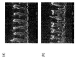
- (A) It is an image which shows the longitudinal cross-section in the part of a cylindrical recessed part.
- (B) It is an image which shows the cross section in the part of a cylindrical recessed part and the cone-shaped convex part (projection part) in it. It is a graph which shows the reflectance characteristic of the optical element which concerns on 1st Embodiment. It is a figure which shows the process of manufacturing the original disk for the optical element which concerns on 1st Embodiment, and the process of manufacturing the replication substrate for optical element production. It is a figure which shows the longitudinal cross-section of a part of stamper formed. It is a photograph of a part of the stamper surface.
- (A) It is a partial top view of the optical element which concerns on 2nd Embodiment.
- (B) It is sectional drawing and perspective view about a part of optical element shown by the top view of (a).
- C) It is a perspective view of the structure arrange
- the optical element according to the embodiment of the present invention is a sheet-like optical element formed by arranging a large number of minute structures on a plane.
- the individual structures are arranged with a pitch of several hundred nm.
- the present inventors have confirmed that the reflectance can be reduced in a wide wavelength band by using the optical element according to the present invention.
- FIG. 1A is a plan view of a part of the optical element 1 according to the first embodiment.
- FIG. 1B is a cross-sectional view and a perspective view of a further part of the optical element 1 shown in the plan view of FIG.
- FIG.1 (c) is a perspective view of the structure 2 arrange
- the optical element 1 is made of a substantially transparent material, and is formed by regularly arranging a large number of minute structures 2 shown in FIGS. 1 (b) and 1 (c).
- a large number of structures 2 are arranged with a track pitch Tp in the vertical direction and a dot pitch Dp in the horizontal direction.
- the horizontal rows of the structures 2 in FIG. 1A are referred to as “tracks”.
- Each structure 2 includes a rectangular parallelepiped main body 100, a columnar recess 101 provided in the main body 100, and a protrusion provided in the recess 101 (hereinafter referred to as “protrusion”). 102). Note that the individual main body portions 100 are not arranged independently, but as will be described later, the main body portions 100 are formed continuously and integrally.
- the recess 101 is cylindrical. That is, the shape of the cross section by the horizontal surface of the recessed part 101 is circular. Moreover, the protrusion part 102 is conical.
- the shape of the transverse cross section of the concave portion 101 may be a polygon such as a triangle or a quadrangle, and the protrusion 102 may be a polygonal shape such as a triangular pyramid or a quadrangular pyramid.
- the structures 2 are arranged in a grid pattern.
- the arrangement of the structures between the tracks is not limited to the grid pattern, but a staggered pattern. It may be.
- other arrangements for example, a random arrangement may be used.
- the sizes of the structures 2 arranged in large numbers that is, the diameter of the recess 101, the diameter or height of the protrusions, etc. may not be uniform.
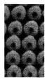
- FIG. 2 is a photographic image showing a partial surface shape of the optical element 1 according to the first embodiment.
- the optical element 1 shown in FIG. 2 is made of an ultraviolet curable resin, and the recesses 101 in the structure 2 are formed at a constant pitch (200 nm in this example).
- the base material forming the optical element 1 is a transparent body and can transmit visible light.
- the refractive index of the substrate is preferably between 1 and 3 which can exist as a transparent body.
- the constant pitch at which the recesses 101 in the structure 2 are disposed is preferably 160 nm to 250 nm, but may be other intervals.
- FIG. 3 is a photographic image showing a cross-sectional structure of the structure 2 of the optical element 1.
- the image shown in FIG. 3A shows a longitudinal section in the cylindrical recess 101 portion.
- the height of the cylindrical recess 101 shown in FIG. 3A is about 375 nm.
- the image shown in FIG. 3 (b) shows a cross section of the cylindrical recess 101 and the conical protrusion 102 therein.
- the height of the conical protrusion 102 shown in FIG. 3B is about 225 nm. Note that the heights of the recesses 101 and the protrusions 102 here are examples.
- FIG. 4 is a graph showing the reflectance characteristics of the optical element 1 according to the first embodiment.
- the horizontal axis indicates the wavelength of light
- the vertical axis indicates the reflectance of light incident perpendicularly at that wavelength.
- FIG. 4 also shows the reflectance characteristics of a commercial film for comparison.
- the commercial film shown in FIG. 4 is of a type having a conventional antireflection film in which films are laminated.
- the reflectance is suppressed at a wavelength of 450 nm or more in the visible range (400 nm to 700 nm).
- the reflectance is 1% or more, and the antireflection effect is not sufficient.
- the reflectance is lower than that of a commercially available film over the entire wavelength range, that is, the reflectance is low without depending on the wavelength.
- the pitch of the arrangement of the structures 2 is set to a size equal to or smaller than the wavelength of light for reducing the reflectance.
- the effect of suppressing the reflectance is enhanced by setting the pitch of the arrangement of the structures 2 to a size that is half or less of the wavelength that is considered as the limit of optical resolution. Therefore, for visible light, it is desirable that the wavelength is not more than 300 nm, which is about half of the longer wavelength of red that can be recognized by the human eye. It is desirable to set it to 250 nm or less which is half or less of the high green wavelength.
- the depth of the concave portion 101 of the structure 2 is at least 200 nm.
- the height of the inner conical protrusion 102 is the same as or smaller than the depth of the cylindrical recess 101. It is desirable to do.
- the ratio of the cross-sectional area of the structure 2 occupying in the horizontal plane by the horizontal plane between the upper surface and the lower surface of the optical element 1 is determined according to the depth. It is desirable to change continuously, and in particular, it is desirable to increase continuously from the opening of the recess 101 toward the back (that is, from the upper surface to the lower surface of the optical element 1). That is, the ratio of the cross-sectional area of the optical element 1 itself in the horizontal plane due to the horizontal plane varies continuously from the upper surface to the lower surface of the optical element 1 (in particular, the recess 101).
- the distance increases continuously from the opening of the optical element (that is, continuously from the upper surface to the lower surface of the optical element 1).
- the inner protruding portion 102 does not protrude from the upper end of the cylindrical recess 101.
- the combination of the shape of the concave portion 101 and the protruding portion 102 may be a columnar shape and a conical shape, a quadrangular prism shape and a quadrangular pyramid shape, etc., but depending on the depth between the upper surface and the lower surface of the optical element 1, Since it is desirable that the ratio of the cross-sectional area of the structure 2 occupying the horizontal plane is continuously changed (increase), the inner protrusion is substantially conical (conical, bell-shaped, Mt. Fuji, etc.) In addition, a shape such as a substantially quadrangular pyramid shape is more desirable.
- the optical element according to the first embodiment can be formed of a material close to a black body that absorbs light, for example, a material mainly composed of carbon black, instead of a transparent material.
- a material close to a black body that absorbs light for example, a material mainly composed of carbon black
- Such an optical element is an optical element having performance as a light absorber with suppressed surface reflection. That is, an optical element having characteristics close to a black body without depending on the wavelength can be realized.
- the material is a metal, for example, Ni, an optical element with reduced reflectance can be obtained.
- the method for manufacturing an optical element according to the first embodiment includes a process for manufacturing a master, a process for manufacturing a replica substrate for manufacturing an optical element, and a process for forming an optical element.
- these steps will be described with respect to some examples of the manufacturing method with reference to the drawings.
- FIG. 5 shows a step of producing a master and a step of producing a replica substrate for producing an optical element in the first example manufacturing method for the optical element according to the first embodiment.
- FIG. 5A a substrate 11 is prepared.
- the substrate 11 may be a silicon wafer, for example.
- an organic layer 12 is formed on the surface of the substrate 11.
- an acrylic resin is used as the organic material layer 12.
- the concentration of the acrylic resin may be 45%, for example, and the thickness may be 400 nm, for example.
- the resist layer 13 may be an inorganic resist, and a transition metal such as a MoW partial oxide film can be used as the inorganic resist.
- the MoW partial oxide film may be formed to a thickness of 30 nm. This resist layer 13 acts as a mask as will be shown later.
- the resist layer 13 on the substrate 11 is irradiated with a laser beam 14 as an exposure beam.
- exposure is performed while rotating the substrate 11 using an exposure apparatus used in optical disk manufacturing.
- the resist layer 13 is exposed over the entire surface by intermittently irradiating the laser beam 14 while moving the substrate 11 in the radial direction.
- the exposure may be performed so that the track pitch (Tp) is 250 m and the dot pitch (Dp) is 250 nm.
- the laser beam 14 for example, a laser beam having a waveform whose amplitude changes periodically or aperiodically is used.
- the dots formed by exposure can be arranged in a lattice pattern or in a dense state.
- Dp dot pitch
- the developer 15 is dropped on the resist layer 13 while rotating the substrate 11, and then the resist layer 13 is developed. Thereby, as shown in FIG.5 (f), the pattern used as the mask for an etching is formed.
- TMAH having a concentration of 2.38% is used as the developer.
- the organic material layer 12 formed on the substrate 11 is etched.
- the hole shape (recessed portion) of the organic layer 12 is formed on the substrate 11.
- the etching method may be performed by dry etching with oxygen gas.
- etching is performed using oxygen gas at a flow rate of 300 sccm for 1 minute.
- the master is formed by the steps so far.
- a conductive film 16 is formed on the substrate 11 shown in FIG.
- the conductive film 16 is formed, for example, by sputtering with Ni (see FIG. 5H). Further, electroforming plating is performed on the substrate 11 shown in FIG. 5 (h) (see FIG. 5 (i)). Electroforming is performed using Ni, for example.
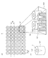
- a stamper (a replica substrate for manufacturing an optical element) 18 shown in FIG. 6 is formed by peeling the conductive film portion and the electroformed plating portion in FIG.
- FIG. 6 is a view showing a longitudinal section of a part of the stamper 18 to be formed.
- FIG. 7 is a photographic image of a part of the surface of the stamper 18.
- the opening of the hole (recessed portion) is formed so that Ni covers the surface of the hole before Ni fills the space of the hole (recessed portion) of the master. It is necessary to adjust the size of the part and the depth of the hole (for the concave part). That is, the size of the opening of the hole (recess portion) and the size of the hole (recess portion) so that the volume of Ni entering the hole (recess portion) is smaller than the volume of the space of the hole (recess portion). It is necessary to adjust the depth.
- substrate structure 20 which comprises the stamper 18 formed as shown in FIG. 6 is not a mere column shape, but becomes a column shape which has the hollow 22 in the center part by lacking Ni. .
- Optical element 1 is formed using stamper 18 created as described above. Specifically, the melted resin is applied to the stamper 18, the applied resin is cooled, and then peeled off from the stamper 18, thereby forming the optical element 11.
- the resin is preferably a material that remains elastic after cooling. In the manufacturing method of the first example, PC or the like is used as the resin.
- a manufacturing method of the second example of the optical element 1 according to the first embodiment will be described.
- the manufacturing method of the second example is basically the same as the manufacturing method of the first example, and a step of manufacturing a master, a step of manufacturing a replica substrate for manufacturing an optical element, and an optical element are formed. Process. Similar to the manufacturing method of the first example, these steps will be described with reference to FIG.
- a substrate 11 is prepared.
- the substrate 11 may be a quartz substrate, sodium glass, or the like, for example.
- an organic layer 12 is formed on the surface of the substrate 11.
- a novolac resin, a chemically amplified resist, or the like is used as the organic layer 12.
- the resist layer 13 may be an inorganic resist, and TePd oxide can be used as the inorganic resist.
- TePd oxide can be used as the inorganic resist.
- the oxide of TePd may be formed as a film having a thickness of 40 nm. This resist layer 13 acts as a mask.
- the resist layer 13 on the substrate 11 is irradiated with a laser beam 14 as an exposure beam. Also in the manufacturing method of the second example, exposure is performed while rotating the substrate 11 using an exposure apparatus used in optical disk manufacturing. In the manufacturing method of the second example, exposure is performed so that the track pitch (Tp) is 200 m and the dot pitch (Dp) is 200 nm.
- the developer 15 is dropped on the resist layer 13 while rotating the substrate 11, and then the resist layer 13 is developed. Thereby, as shown in FIG.5 (f), the pattern used as the mask for an etching is formed.
- an inorganic developer made by Rohm and Haas is used as the developer.
- the organic material layer 12 formed on the substrate 11 is etched. Thereby, as shown in FIG. 5G, the hole shape (recessed portion) of the organic layer 12 is formed on the substrate 11.
- the etching method for example, dry etching using argon gas may be performed.
- etching is performed using argon gas at a flow rate of 400 sccm for 5 minutes. The master is formed by the steps so far.
- Step of Producing Optical Element Fabricating Duplicate Substrate Conductive film 16 is formed on substrate 11 shown in FIG. 5G after etching.
- the conductive film 16 is formed, for example, by sputtering using a Ni partial oxide film (see FIG. 5H).
- electroforming plating 17 is performed on the substrate 11 shown in FIG. 5 (h) (see FIG. 5 (i)). The electroforming is performed using, for example, Ni.
- a stamper (a duplicated substrate for manufacturing an optical element) 18 shown in FIG. 6 is formed by peeling the conductive film portion and the electroformed plating portion shown in FIG.
- Optical element 1 is formed using stamper 18 created as described above. Specifically, the optical element 1 is formed by applying a UV curable resin to the stamper 18, curing the applied UV curable resin with UV light, and then peeling the stamper 18.
- the UV curable resin is desirably a material that remains elastic after cooling.
- PMMA or the like is used as the UV curable resin.
- a manufacturing method of the third example of the optical element 1 according to the first embodiment will be described.
- the manufacturing method of the third example is basically the same as the manufacturing method of the first example, and a step of manufacturing a master, a step of manufacturing a replica substrate for manufacturing an optical element, and an optical element are formed. Process. Similar to the manufacturing method of the first example, these steps will be described with reference to FIG.
- Step of Producing Master A step of preparing the substrate 11 (FIG. 5A) and a step of forming the organic layer 12 (FIG. 5B) are performed in the same manner as the production method of the second example.
- the resist layer 13 may be an inorganic resist, and Ni can be used as the inorganic resist. Ni may be formed as a film having a thickness of 40 nm. This resist layer 13 acts as a mask.
- the step of irradiating the resist layer 13 with the laser beam 14 (FIG. 5D) and the step of developing the resist layer 13 (FIG. 5E) are the same as in the manufacturing method of the second example. Done.
- the organic material layer 12 formed on the substrate 11 is etched.
- the hole shape (recessed portion) of the organic layer 12 is formed on the substrate 11.
- etching method for example, it may be performed by dry etching with CHF3.
- etching is performed using CHF3 at a flow rate of 400 sccm for 3 minutes.
- the master is formed by the steps so far.
- Step of manufacturing a replica substrate for producing an optical element A conductive film 16 and an electrocast plating 17 are formed on the etched substrate 11 (FIGS. 5 (h) and (i)), and the formed conductive film portion and electrocast
- the step of forming a stamper (optical element manufacturing replica substrate) 18 by peeling the plated portion from the substrate 11 (FIG. 6) is performed in the same manner as in the manufacturing method of the second example.
- Optical element 1 is formed using stamper 18 created as described above. Specifically, the optical element 1 is formed by performing injection molding using the stamper 18 as a mold. In order to ensure releasability from the stamper 18, it is desirable that the resin for injection molding is a material that remains elastic even when peeled. In the manufacturing method of the third example, PET or the like is used as the resin for injection molding.
- the manufacturing method of the optical element according to the first embodiment is not limited to the above.
- the optical element can also be formed by arranging a sheet on the back surface of a resin (such as a UV curable resin) and peeling the resin and the sheet from the stamper 18 so that the ultraviolet curable resin remains on the sheet.
- a resin such as a UV curable resin
- the structure 2 includes a rectangular parallelepiped main body 100, a columnar recess 101 provided in the main body 100, and a protrusion (protrusion) provided in the recess 101.
- a protrusion protrusion
- FIG. 8A is a plan view of a part of the optical element 1 ′ according to the second embodiment.
- FIG. 8B is a cross-sectional view and a perspective view of a further part of the optical element 1 ′ shown in the plan view of FIG.
- FIG. 8C is a perspective view of the structure 2 ′ disposed in the optical element 1 ′ according to the second embodiment.
- the structure 2 ′ includes the structure 2 in the optical element 1 according to the first embodiment shown in FIG. The shape is reversed.
- the optical element 1 ′ according to the second embodiment is also made of a substantially transparent material, and the minute structure 2 ′ shown in FIGS. 8B and 8C has a track pitch Tp in the vertical direction and a horizontal direction. Many dots are regularly arranged at a dot pitch Dp.
- Each structural body 2 ′ includes a convex portion 101 ′ and a concave portion (hereinafter referred to as “dent”) 102 ′ provided inside from the surface of the convex portion 101 ′. Further, the structure 2 ′ is disposed on a planar sheet 103 ′ made of the same material as the structure 2 ′.
- the convex portion 101 ′ has a cylindrical shape.
- the recess 102 ' has a conical shape, but has a shape in which the cone is inverted. That is, the recess 102 ′ has a large cross-sectional area at the opening on the upper surface of the structure 2 ′, and the cross-sectional area becomes smaller toward the lower surface of the structure 2 ′. Further, the depth of the recess 102 'is smaller than the height of the convex portion 101'.
- the convex portion 101 ′ may have a polygonal prism shape such as a triangular prism shape or a quadrangular prism shape.
- the recess 102 ′ may have a polygonal pyramid shape such as a triangular pyramid shape or a quadrangular pyramid shape.
- the structures 2 ′ are arranged in a grid pattern, but the arrangement of the structures 2 ′ between the tracks is not limited to the grid pattern, A staggered arrangement or other arrangements may be used.
- the optical element 1 ′ according to the second embodiment shown in FIG. 8 is different from the first to third example manufacturing methods for the optical element 1 according to the first embodiment described above. 6 is manufactured by a manufacturing method including a step of creating a stamper in which the unevenness of the stamper 18 shown in 6 is reversed. Similar to the optical element 1 according to the first embodiment, the optical element 1 ′ according to the second embodiment having such a configuration can obtain an effect of reducing the reflectance.
- the optical element according to the embodiment of the present invention is formed by arranging a large number of minute structures in a planar shape. For this reason, the optical element according to the embodiment can reduce the reflectance with respect to a wide wavelength band.
- the present invention relates to an optical element whose optical characteristics are controlled by a surface structure and a method for manufacturing the same, and more particularly to an optical element for reducing the reflectance on the surface by a structure and a method for manufacturing the same.
- the optical element according to the present invention is useful for preventing reflection of a display. Further, it can be applied to uses such as preventing flare in a lens barrel.
Abstract
Description
表面に可視光の波長よりも小さい間隔で、凹部及び凸部のいずれか一方が複数配置され、前記凹部及び凸部のうちの配置された一方において、前記凹部及び凸部のうちの配置されなかった他方が形成されたことを特徴とする。 The present invention has been made to solve the above problems. The optical element according to the present invention is
A plurality of concave portions and convex portions are arranged on the surface at intervals smaller than the wavelength of visible light, and one of the concave portions and the convex portions is not arranged, of the concave portions and the convex portions. The other is formed.
表面に可視光の波長よりも小さい間隔で、凹部及び凸部のいずれか一方が複数配置され、前記凹部及び凸部のうちの配置された一方において、前記凹部及び凸部のうちの配置されなかった他方が形成された光学素子のための、光学素子作製用複製基板の製造方法において、
基板の表面に有機物層を形成する第1の工程と、
前記有機物層の表面にレジスト層を形成する第2の工程と、
前記レジスト層にレーザー光を前記基板を移動させながら間欠的に照射して露光する第3の工程と、
前記レジスト層を現像処理し、エッチングのマスクパターンを形成する第4の工程と、
前記マスクパターンをマスクとするエッチング処理を行うことで、前記基板の表面に凹凸構造を形成する第5の工程と、
前記凹凸構造を有する前記基板の表面に、導電膜をスパッタリングし、更に加えて電気鋳造メッキを行なう第6の工程であって、電気鋳造メッキを行なう際に前記凹凸構造の凹部分の空間を電気鋳造メッキで用いる金属が埋め尽くす前に、前記金属が前記凹部分の表面を覆ってしまうように、前記凹部分の開口部の寸法及び前記凹部分の深さが調整されている、第6の工程と、
前記導電膜部分及び電気鋳造メッキ部分を、前記凹凸構造を有する前記基板の表面から剥離することで、複製基板を作製する第7の工程と
を備える。 In addition, the method for producing a replica substrate for producing an optical element according to the present invention includes:
A plurality of concave portions and convex portions are arranged on the surface at intervals smaller than the wavelength of visible light, and one of the concave portions and the convex portions is not arranged, of the concave portions and the convex portions. In the method of manufacturing a replica substrate for producing an optical element for the optical element on which the other is formed,
A first step of forming an organic layer on the surface of the substrate;
A second step of forming a resist layer on the surface of the organic layer;
A third step of exposing the resist layer by intermittently irradiating a laser beam while moving the substrate;
A fourth step of developing the resist layer to form an etching mask pattern;
A fifth step of forming an uneven structure on the surface of the substrate by performing an etching process using the mask pattern as a mask;
In the sixth step, a conductive film is sputtered on the surface of the substrate having the concavo-convex structure, and additionally electrocast plating is performed, and when the electrocast plating is performed, the space corresponding to the concave portion of the concavo-convex structure is electrically Before the metal used in the casting plating is filled, the dimension of the opening of the recess and the depth of the recess are adjusted so that the metal covers the surface of the recess. Process,
A seventh step of producing a duplicate substrate by peeling the conductive film portion and the electroformed plating portion from the surface of the substrate having the concavo-convex structure.
本発明に係る光学素子作製用複製基板の製造方法で製造された複製基板を用いる光学素子の製造方法であって、
前記複製基板の表面に溶解した樹脂を塗布する第1の工程と、
塗布した溶解した樹脂を冷却させ、前記複製基板から剥離することで光学素子を形成する第2の工程と
を備える。 Furthermore, the manufacturing method of the optical element according to the present invention includes:
A method for manufacturing an optical element using a replica substrate manufactured by the method for manufacturing a replica substrate for producing an optical element according to the present invention,
A first step of applying a dissolved resin to the surface of the replication substrate;
And a second step of forming an optical element by cooling the applied dissolved resin and peeling it from the replication substrate.
以下、本発明に係る第1の実施の形態について、図面を参照しつつ説明する。 <First Embodiment>
A first embodiment according to the present invention will be described below with reference to the drawings.
図1(a)は、第1の実施の形態に係る光学素子1の一部の平面図である。図1(b)は、図1(a)の平面図に示される光学素子1の更に一部についての断面図及び斜視図である。更に、図1(c)は、第1の実施の形態に係る光学素子1に配置される構造体2の斜視図である。 1. Configuration of Optical Element FIG. 1A is a plan view of a part of the
個々の構造体2は、直方体形状の本体部100と、本体部100に設けられた円柱状の凹部101と、凹部101の中に設けられた凸部(以下、「突出部」という)102とにより構成される。なお、個々の本体部100は独立して配置されるのではなく、後で説明するように、本体部100同士は連続的且つ一体的に形成されている。 1.1. Structure Structure Each
図2は、第1の実施の形態に係る光学素子1の一部の表面形状を示す写真画像である。図2に示す光学素子1は、紫外線硬化樹脂により構成されており、構造体2における凹部101は一定のピッチ(本例では、200nm)で形成されている。 1.2. Configuration Example of Structure FIG. 2 is a photographic image showing a partial surface shape of the
図4は、第1の実施の形態に係る光学素子1の反射率特性を示すグラフである。図4のグラフにおいて、横軸は光の波長、縦軸はその波長での垂直に入射する光の反射率を示す。 2. Reflectivity Characteristics of Optical Element FIG. 4 is a graph showing the reflectance characteristics of the
次に、第1の実施の形態に係る光学素子1の製造方法のいくつかの例について説明する。第1の実施の形態に係る光学素子の製造方法は、原盤を製造する工程と、光学素子作製用複製基板を製造する工程と、光学素子を形成する工程とを含む。以下、図面を参照しながら、いくつかの製造方法の例について、これらの工程を説明する。 3. Next, several examples of the method for manufacturing the
3.1.1.原盤を製造する工程
図5は、第1の実施の形態に係る光学素子のための、第1の例の製造方法における、原盤を製造する工程と光学素子作製用複製基板を製造する工程を示す図である。まず、図5(a)に示すように、基板11を準備する。この基板11は、例えば、シリコンウエハなどであればよい。 3.1. Production method of the first example 3.1.1. Step of Producing Master FIG. 5 shows a step of producing a master and a step of producing a replica substrate for producing an optical element in the first example manufacturing method for the optical element according to the first embodiment. FIG. First, as shown in FIG. 5A, a
次に、エッチングを行った図5(g)に示す基板11上に導電膜16を形成する。導電膜16は、例えば、Niによるスパッタリングにより形成される(図5(h)参照)。更に、図5(h)に示す基板11に対して、電気鋳造メッキを行う(図5(i)参照)。電気鋳造は、例えばNiを用いて行われる。 3.1.2. Step of Manufacturing Duplicated Substrate for Optical Element Fabrication Next, a
以上のようにして作成したスタンパ18を用いて光学素子1が形成される。具体的には、スタンパ18に、溶解した樹脂を塗布し、塗布した樹脂を冷却させた後、スタンパ18から剥離することで光学素子11が形成される。スタンパ18からの剥離性を確保するため、樹脂は、冷却後も弾性が残る材料であることが望ましい。第1の例の製造方法では、樹脂としてPC等を用いる。 3.1.3. Step of Forming Optical
第1の実施の形態に係る光学素子1の、第2の例の製造方法について説明する。第2の例の製造方法は、基本的に第1の例の製造方法と同様のものであり、原盤を製造する工程と、光学素子作製用複製基板を製造する工程と、光学素子を形成する工程とを含む。第1の例の製造方法の場合と同様に図5を用いて、これらの工程を説明する。 3.2. Manufacturing Method of Second Example A manufacturing method of the second example of the
図5(a)に示すように、基板11を準備する。この基板11は、例えば、石英基板、ナトリウムガラスなどであればよい。 3.2.1. Process for Producing Master Plate As shown in FIG. 5A, a
エッチングを行った図5(g)に示す基板11上に導電膜16を形成する。導電膜16は、例えば、Niの部分酸化膜によるスパッタリングにより形成される(図5(h)参照)。更に、図5(h)に示す基板11に対して、電気鋳造メッキ17を行う(図5(i)参照)。電気鋳造は、例えば、Niを用いて行われる。 3.2.2. Step of Producing Optical Element Fabricating Duplicate
以上のようにして作成したスタンパ18を用いて光学素子1が形成される。具体的には、スタンパ18に、UV硬化樹脂を塗布し、塗布したUV硬化樹脂をUV光にて硬化させた後、スタンパ18から剥離することで光学素子1が形成される。スタンパ18からの剥離性を確保するため、UV硬化樹脂は、冷却後も弾性が残る材料であることが望ましい。第2の例の製造方法では、UV硬化樹脂としてPMMA等を用いる。 3.2.3. Step of Forming Optical
第1の実施の形態に係る光学素子1の、第3の例の製造方法について説明する。第3の例の製造方法も、基本的に第1の例の製造方法と同様のものであり、原盤を製造する工程と、光学素子作製用複製基板を製造する工程と、光学素子を形成する工程とを含む。第1の例の製造方法の場合と同様に図5を用いて、これらの工程を説明する。 3.3. Manufacturing Method of Third Example A manufacturing method of the third example of the
基板11を準備する工程(図5(a))、及び有機物層12を形成する工程(図5(b))が、第2の例の製造方法と同様に行なわれる。 3.3.1. Step of Producing Master A step of preparing the substrate 11 (FIG. 5A) and a step of forming the organic layer 12 (FIG. 5B) are performed in the same manner as the production method of the second example.
エッチングを行った基板11上に導電膜16及び電気鋳造メッキ17を形成し(図5(h)、(i))、形成された導電膜部分及び電気鋳造メッキ部分を基板11から剥離することにより、スタンパ(光学素子作製用複製基板)18が形成される(図6)工程も、第2の例の製造方法と同様に行なわれる。 3.3.2. Step of manufacturing a replica substrate for producing an optical element A
以上のようにして作成したスタンパ18を用いて光学素子1が形成される。具体的には、スタンパ18を金型として用いて、射出成形を行うことにより光学素子1が形成される。スタンパ18からの剥離性を確保するため、射出成形の樹脂は、剥離時にも弾性が残る材料であることが望ましい。第3の例の製造方法では、射出形成の樹脂としてPET等を用いる。 3.3.3. Step of Forming Optical
第1の実施の形態に係る光学素子の製造方法は、以上のものに限定されない。例えば、(UV硬化樹脂等の)樹脂の背面にシートを配し、シートに紫外線硬化樹脂が残るようにしてスタンパ18から樹脂及びシートを剥離することでも、光学素子を形成することができる。 3.4. Other Manufacturing Methods The manufacturing method of the optical element according to the first embodiment is not limited to the above. For example, the optical element can also be formed by arranging a sheet on the back surface of a resin (such as a UV curable resin) and peeling the resin and the sheet from the
上述の第1の実施の形態では、構造体2は、直方体形状の本体部100と、本体部100に設けられた円柱状の凹部101と、凹部101の中に設けられた凸部(突出部)102とにより形成したが、別の形状であっても単体の円柱形状や円錐形状よりも微細な構造であれば、その形状に捉われず同様の効果を得ることができる。 <Second Embodiment>
In the first embodiment described above, the
以上のように、本発明の実施の形態に係る光学素子は、平面状に多数の微小な構造体を配置して形成される。このため、実施の形態に係る光学素子は、広い波長帯域に関して反射率を低減できるものとなっている。 <Summary>
As described above, the optical element according to the embodiment of the present invention is formed by arranging a large number of minute structures in a planar shape. For this reason, the optical element according to the embodiment can reduce the reflectance with respect to a wide wavelength band.
Claims (20)
- 表面に可視光の波長よりも小さい間隔で、凹部及び凸部のいずれか一方が複数配置され、前記凹部及び凸部のうちの配置された一方において、前記凹部及び凸部のうちの配置されなかった他方が形成されたことを特徴とする光学素子。 A plurality of concave portions and convex portions are arranged on the surface at intervals smaller than the wavelength of visible light, and one of the concave portions and the convex portions is not arranged, of the concave portions and the convex portions. An optical element characterized in that the other is formed.
- 前記凹部の中に前記凸部が形成されたことを特徴とする請求項1に記載の光学素子。 The optical element according to claim 1, wherein the convex portion is formed in the concave portion.
- 前記凹部の水平面による横断面の形状が、円形又は多角形であることを特徴とする請求項2に記載の光学素子。 3. The optical element according to claim 2, wherein a shape of a cross section of the concave portion by a horizontal plane is a circle or a polygon.
- 前記凸部が、円錐状又は多角垂状であることを特徴とする請求項2に記載の光学素子。 The optical element according to claim 2, wherein the convex portion is conical or polygonal.
- 前記凹部の深さが、前記凸部の高さより大きいことを特徴とする請求項2に記載の光学素子。 3. The optical element according to claim 2, wherein the depth of the concave portion is larger than the height of the convex portion.
- 前記凸部上に前記凹部が形成されたことを特徴とする請求項1に記載の光学素子。 The optical element according to claim 1, wherein the concave portion is formed on the convex portion.
- 前記凸部が、円柱状又は多角柱状であることを特徴とする請求項6に記載の光学素子。 The optical element according to claim 6, wherein the convex portion has a columnar shape or a polygonal columnar shape.
- 前記凹部が、円錐状又は多角錘状である請求項6に記載の光学素子。 The optical element according to claim 6, wherein the concave portion has a conical shape or a polygonal pyramid shape.
- 前記凸部の高さが、前記凹部の深さより大きいことを特徴とする請求項6に記載の光学素子。 The optical element according to claim 6, wherein a height of the convex portion is larger than a depth of the concave portion.
- 前記複数配置された凹部又は凸部が、格子状に配置されていることを特徴とする請求項1に記載の光学素子。 2. The optical element according to claim 1, wherein the plurality of concave portions or convex portions are arranged in a lattice shape.
- 前記複数配置された凹部又は凸部の、配置されるドットピッチ(Dp)に対する、前記凹部又は凸部の径(r)の比率が、70%以上であるように、前記凹部又は凸部が配置されていることを特徴とする請求項1に記載の光学素子。 The concave or convex portions are arranged such that the ratio of the diameter (r) of the concave or convex portions to the arranged dot pitch (Dp) of the plurality of concave or convex portions is 70% or more. The optical element according to claim 1, wherein the optical element is formed.
- 前記配置された凹部又は凸部の配置の間隔が、250nm以下160nm以上であることを特徴とする請求項1に記載の光学素子。 2. The optical element according to claim 1, wherein an interval between the arranged concave portions or convex portions is 250 nm or less and 160 nm or more.
- 前記光学素子を形成する基材が、可視光を透過可能であることを特徴とする請求項1に記載の光学素子。 2. The optical element according to claim 1, wherein the base material forming the optical element is capable of transmitting visible light.
- 前記基材の屈折率が1から3の間にあることを特徴とする請求項13に記載の光学素子。 The optical element according to claim 13, wherein the refractive index of the substrate is between 1 and 3.
- 前記光学素子を形成する基材が、光を吸収する略黒体であり、光の反射を抑えて光を吸収することを特徴とする請求項1に記載の光学素子。 The optical element according to claim 1, wherein the base material forming the optical element is a substantially black body that absorbs light and absorbs light while suppressing reflection of light.
- 前記光学素子の上面から下面までの間で、深さに応じて、水平面による横断平面の中に占める前記光学素子そのものの横断面積の割合が、前記光学素子の上面から下面に向かうほど連続的に増加することを特徴とする請求項1に記載の光学素子。 Between the upper surface and the lower surface of the optical element, the ratio of the cross-sectional area of the optical element itself in the horizontal transverse plane according to the depth is continuously increased from the upper surface to the lower surface of the optical element. The optical element according to claim 1, wherein the optical element increases.
- 表面に可視光の波長よりも小さい間隔で、凹部及び凸部のいずれか一方が複数配置され、前記凹部及び凸部のうちの配置された一方において、前記凹部及び凸部のうちの配置されなかった他方が形成された光学素子のための、光学素子作製用複製基板の製造方法において、
基板の表面に有機物層を形成する第1の工程と、
前記有機物層の表面にレジスト層を形成する第2の工程と、
前記レジスト層にレーザー光を前記基板を移動させながら間欠的に照射して露光する第3の工程と、
前記レジスト層を現像処理し、エッチングのマスクパターンを形成する第4の工程と、
前記マスクパターンをマスクとするエッチング処理を行うことで、前記基板の表面に凹凸構造を形成する第5の工程と、
前記凹凸構造を有する前記基板の表面に、導電膜をスパッタリングし、更に加えて電気鋳造メッキを行なう第6の工程であって、電気鋳造メッキを行なう際に前記凹凸構造の凹部分の空間を電気鋳造メッキで用いる金属が埋め尽くす前に、前記金属が前記凹部分の表面を覆ってしまうように、前記凹部分の開口部の寸法及び前記凹部分の深さが調整されている、第6の工程と、
前記導電膜部分及び電気鋳造メッキ部分を、前記凹凸構造を有する前記基板の表面から剥離することで、複製基板を作製する第7の工程と
を備える光学素子作製用複製基板の製造方法。 A plurality of concave portions and convex portions are arranged on the surface at intervals smaller than the wavelength of visible light, and one of the concave portions and the convex portions is not arranged, of the concave portions and the convex portions. In the method of manufacturing a replica substrate for producing an optical element for the optical element on which the other is formed,
A first step of forming an organic layer on the surface of the substrate;
A second step of forming a resist layer on the surface of the organic layer;
A third step of exposing the resist layer by intermittently irradiating a laser beam while moving the substrate;
A fourth step of developing the resist layer to form an etching mask pattern;
A fifth step of forming an uneven structure on the surface of the substrate by performing an etching process using the mask pattern as a mask;
In the sixth step, a conductive film is sputtered on the surface of the substrate having the concavo-convex structure, and additionally electrocast plating is performed, and when the electrocast plating is performed, the space corresponding to the concave portion of the concavo-convex structure is electrically Before the metal used in the casting plating is filled, the dimension of the opening of the recess and the depth of the recess are adjusted so that the metal covers the surface of the recess. Process,
A method of manufacturing a replica substrate for manufacturing an optical element, comprising: a seventh step of manufacturing a replica substrate by peeling the conductive film portion and the electroformed plating portion from the surface of the substrate having the concavo-convex structure. - 請求項17記載の光学素子作製用複製基板の製造方法で製造された複製基板を用いる光学素子の製造方法であって、
前記複製基板の表面に溶解した樹脂を塗布する第1の工程と、
塗布した溶解した樹脂を冷却させ、前記複製基板から剥離することで光学素子を形成する第2の工程と
を備える光学素子の製造方法。 A method for producing an optical element using a duplicate substrate produced by the method for producing a duplicate substrate for producing an optical element according to claim 17,
A first step of applying a dissolved resin to the surface of the replication substrate;
A method of manufacturing an optical element, comprising: a second step of forming the optical element by cooling the applied dissolved resin and peeling it from the replication substrate. - 請求項17記載の光学素子作製用複製基板の製造方法で製造された複製基板を用いる光学素子の製造方法であって、
前記複製基板の表面にUV硬化樹脂を塗布する第1の工程と、
塗布したUV硬化樹脂を硬化させ、前記複製基板から剥離することで光学素子を形成する第2の工程と
を備えた光学素子の製造方法。 A method for producing an optical element using a duplicate substrate produced by the method for producing a duplicate substrate for producing an optical element according to claim 17,
A first step of applying a UV curable resin to the surface of the replication substrate;
A method of manufacturing an optical element, comprising: a second step of curing the applied UV curable resin and forming the optical element by peeling off from the replication substrate. - 請求項17記載の光学素子作製用複製基板の製造方法で製造された複製基板を用いる光学素子の製造方法であって、
前記複製基板を金型として射出成形を行う第1の工程
を備えた光学素子の製造方法。 A method for producing an optical element using a duplicate substrate produced by the method for producing a duplicate substrate for producing an optical element according to claim 17,
An optical element manufacturing method comprising a first step of performing injection molding using the duplicate substrate as a mold.
Priority Applications (4)
| Application Number | Priority Date | Filing Date | Title |
|---|---|---|---|
| JP2012502988A JP5490216B2 (en) | 2010-03-02 | 2011-02-18 | Optical element and optical element manufacturing method |
| US13/579,076 US20120307368A1 (en) | 2010-03-02 | 2011-02-18 | Optical element and method of manufacturing optical elements |
| EP11750322.7A EP2544030A4 (en) | 2010-03-02 | 2011-02-18 | Optical element and method of manufacturing optical elements |
| CN2011800104490A CN102763008A (en) | 2010-03-02 | 2011-02-18 | Optical element and method of manufacturing optical elements |
Applications Claiming Priority (4)
| Application Number | Priority Date | Filing Date | Title |
|---|---|---|---|
| JP2010045144 | 2010-03-02 | ||
| JP2010-045144 | 2010-03-02 | ||
| JP2010-045143 | 2010-03-02 | ||
| JP2010045143 | 2010-03-02 |
Publications (1)
| Publication Number | Publication Date |
|---|---|
| WO2011108208A1 true WO2011108208A1 (en) | 2011-09-09 |
Family
ID=44541878
Family Applications (1)
| Application Number | Title | Priority Date | Filing Date |
|---|---|---|---|
| PCT/JP2011/000908 WO2011108208A1 (en) | 2010-03-02 | 2011-02-18 | Optical element and method of manufacturing optical elements |
Country Status (5)
| Country | Link |
|---|---|
| US (1) | US20120307368A1 (en) |
| EP (1) | EP2544030A4 (en) |
| JP (1) | JP5490216B2 (en) |
| CN (1) | CN102763008A (en) |
| WO (1) | WO2011108208A1 (en) |
Cited By (1)
| Publication number | Priority date | Publication date | Assignee | Title |
|---|---|---|---|---|
| WO2018139359A1 (en) * | 2017-01-24 | 2018-08-02 | 王子ホールディングス株式会社 | Antireflection structure |
Families Citing this family (4)
| Publication number | Priority date | Publication date | Assignee | Title |
|---|---|---|---|---|
| CN103353626B (en) * | 2013-06-13 | 2016-04-20 | 北京大学深圳研究生院 | Three dimensional grating anti-reflection structure and components and parts |
| CN103345007B (en) * | 2013-07-12 | 2016-06-29 | 南昌欧菲光学技术有限公司 | Transparent base and containing the transparent conductive element of this transparent base and optics |
| CN106466926A (en) * | 2015-08-19 | 2017-03-01 | 普昱光电股份有限公司 | Optical element manufacturing method |
| CN105676321B (en) * | 2016-03-14 | 2018-01-05 | 淮阴工学院 | A kind of preparation method of lenticule nano-pore mixing array structure |
Citations (6)
| Publication number | Priority date | Publication date | Assignee | Title |
|---|---|---|---|---|
| JP2008158013A (en) | 2006-12-20 | 2008-07-10 | Sony Corp | Optical element, its manufacturing method, duplicate substrate for fabricating optical element and its manufacturing method |
| JP2008176076A (en) | 2007-01-18 | 2008-07-31 | Sony Corp | Optical element and its manufacturing method, and replicate substrate for manufacturing optical element and its manufacturing method |
| JP2008209867A (en) * | 2007-02-28 | 2008-09-11 | Mitsubishi Rayon Co Ltd | Stamper, glare-proof antireflection article, and its manufacturing method |
| JP2008304637A (en) | 2007-06-06 | 2008-12-18 | Sony Corp | Optical device and its manufacturing method, and duplicate substrate for preparing optical device and its manufacturing method |
| JP2009109755A (en) | 2007-10-30 | 2009-05-21 | Sony Corp | Optical element and method of manufacturing master disk for producing optical element |
| JP2009237135A (en) * | 2008-03-26 | 2009-10-15 | Hoya Corp | Method of forming concave/convex structure and substrate with concave/convex structure |
Family Cites Families (10)
| Publication number | Priority date | Publication date | Assignee | Title |
|---|---|---|---|---|
| CN1950724A (en) * | 2004-05-12 | 2007-04-18 | 松下电器产业株式会社 | Optical element and manufacturing method thereof |
| US7850319B2 (en) * | 2004-05-27 | 2010-12-14 | Panasonic Corporation | Light-absorbing member |
| CN101566699B (en) * | 2004-12-03 | 2015-12-16 | 夏普株式会社 | The manufacture method of antireflection material, optical element, display device and pressing mold and employ the manufacture method of antireflection material of pressing mold |
| JP2007264594A (en) * | 2006-03-01 | 2007-10-11 | Nissan Motor Co Ltd | Anti-reflection fine structure, anti-reflection molded body, method of producing the same |
| JP5105771B2 (en) * | 2006-05-15 | 2012-12-26 | パナソニック株式会社 | Anti-reflection structure and optical device having the same |
| CN101825730B (en) * | 2006-08-21 | 2012-07-04 | 索尼株式会社 | Optical element, method for manufacturing master for manufacturing optical element, and photoelectric conversion device |
| WO2009147858A1 (en) * | 2008-06-06 | 2009-12-10 | シャープ株式会社 | Antireflection film, optical element comprising antireflection film, stamper, process for producing stamper, and process for producing antireflection film |
| CN101952746B (en) * | 2008-07-16 | 2013-07-17 | 索尼公司 | Optical element |
| JP5257066B2 (en) * | 2008-12-26 | 2013-08-07 | ソニー株式会社 | Optical element, display device, optical component with antireflection function, and master |
| US8741417B2 (en) * | 2010-04-16 | 2014-06-03 | Korea University Research And Business Foundation | Films having switchable reflectivity |
-
2011
- 2011-02-18 CN CN2011800104490A patent/CN102763008A/en active Pending
- 2011-02-18 JP JP2012502988A patent/JP5490216B2/en not_active Expired - Fee Related
- 2011-02-18 WO PCT/JP2011/000908 patent/WO2011108208A1/en active Application Filing
- 2011-02-18 US US13/579,076 patent/US20120307368A1/en not_active Abandoned
- 2011-02-18 EP EP11750322.7A patent/EP2544030A4/en not_active Withdrawn
Patent Citations (6)
| Publication number | Priority date | Publication date | Assignee | Title |
|---|---|---|---|---|
| JP2008158013A (en) | 2006-12-20 | 2008-07-10 | Sony Corp | Optical element, its manufacturing method, duplicate substrate for fabricating optical element and its manufacturing method |
| JP2008176076A (en) | 2007-01-18 | 2008-07-31 | Sony Corp | Optical element and its manufacturing method, and replicate substrate for manufacturing optical element and its manufacturing method |
| JP2008209867A (en) * | 2007-02-28 | 2008-09-11 | Mitsubishi Rayon Co Ltd | Stamper, glare-proof antireflection article, and its manufacturing method |
| JP2008304637A (en) | 2007-06-06 | 2008-12-18 | Sony Corp | Optical device and its manufacturing method, and duplicate substrate for preparing optical device and its manufacturing method |
| JP2009109755A (en) | 2007-10-30 | 2009-05-21 | Sony Corp | Optical element and method of manufacturing master disk for producing optical element |
| JP2009237135A (en) * | 2008-03-26 | 2009-10-15 | Hoya Corp | Method of forming concave/convex structure and substrate with concave/convex structure |
Non-Patent Citations (3)
| Title |
|---|
| ERIC B. GRANN ET AL., J. OPTI. SOC. AM. A, vol. 12, no. 2, 1995, pages 333 |
| KAZUYA HAYASHIBE ET AL., SID 09 DIGEST, 2009, pages 303 |
| See also references of EP2544030A4 * |
Cited By (3)
| Publication number | Priority date | Publication date | Assignee | Title |
|---|---|---|---|---|
| WO2018139359A1 (en) * | 2017-01-24 | 2018-08-02 | 王子ホールディングス株式会社 | Antireflection structure |
| JP2018120047A (en) * | 2017-01-24 | 2018-08-02 | 王子ホールディングス株式会社 | Antireflection structure |
| US11016222B2 (en) | 2017-01-24 | 2021-05-25 | Oji Holdings Corporation | Antireflective structure |
Also Published As
| Publication number | Publication date |
|---|---|
| JPWO2011108208A1 (en) | 2013-06-20 |
| EP2544030A1 (en) | 2013-01-09 |
| CN102763008A (en) | 2012-10-31 |
| JP5490216B2 (en) | 2014-05-14 |
| US20120307368A1 (en) | 2012-12-06 |
| EP2544030A4 (en) | 2014-09-03 |
Similar Documents
| Publication | Publication Date | Title |
|---|---|---|
| JP4539657B2 (en) | Anti-reflection optical element | |
| TWI387782B (en) | Optical element, method for producing same, replica substrate for forming optical element, and method for producing replica substrate | |
| US9664821B2 (en) | Optical element and method for manufacturing master for producing optical element | |
| JP5490216B2 (en) | Optical element and optical element manufacturing method | |
| KR20110036875A (en) | Optical element | |
| TW201741726A (en) | Diffusion plate and projection-type projector apparatus | |
| JPWO2005109042A1 (en) | Optical element and manufacturing method thereof | |
| JP5081443B2 (en) | OPTICAL ELEMENT AND ITS MANUFACTURING METHOD, OPTICAL ELEMENT MANUFACTURING REPLICATION BOARD AND ITS MANUFACTURING METHOD | |
| JP2004012856A (en) | Optical element, mold for optical element, and method for manufacturing optical element | |
| JP2008158013A5 (en) | ||
| JP2022186895A (en) | Concavo-convex structure, optical member, and electronic device | |
| JPWO2006129514A1 (en) | Fine lattice and its mold | |
| JP5257131B2 (en) | Manufacturing method of optical element, master for manufacturing optical element, and manufacturing method thereof | |
| US20220128742A1 (en) | Diffuser plate | |
| JP2008203812A (en) | Moth-eye structure and manufacturing method of moth-eye structure | |
| TWI816726B (en) | Master disk, transfer material and method of manufacturing master disk | |
| JP2006243633A (en) | Manufacturing method of member having antireflection structure body | |
| JP4820871B2 (en) | Antireflection structure and manufacturing method thereof | |
| JP2005156989A (en) | Lens barrel | |
| JP5671843B2 (en) | Tray for dry etching, dry etching method using the same, method for producing tray, and method for producing mold | |
| JP2021099399A (en) | Lens for terahertz wave and method for manufacturing lens for terahertz wave | |
| JP2010152411A (en) | Optical element and its manufacturing method, and replicate substrate for manufacturing optical element and its manufacturing method | |
| JP2021099400A (en) | Optical element for terahertz waves and method for manufacturing optical element for terahertz waves | |
| JP2005271410A (en) | Manufacturing method of die for forming antireflection structure, antireflection structure, and optical element | |
| JP2005205642A (en) | Manufacturing method for mold for optical element, mold for optical element, optical element manufacturing method, antireflection structure and optical element |
Legal Events
| Date | Code | Title | Description |
|---|---|---|---|
| WWE | Wipo information: entry into national phase |
Ref document number: 201180010449.0 Country of ref document: CN |
|
| 121 | Ep: the epo has been informed by wipo that ep was designated in this application |
Ref document number: 11750322 Country of ref document: EP Kind code of ref document: A1 |
|
| WWE | Wipo information: entry into national phase |
Ref document number: 13579076 Country of ref document: US Ref document number: 2012502988 Country of ref document: JP |
|
| WWE | Wipo information: entry into national phase |
Ref document number: 2011750322 Country of ref document: EP |
|
| NENP | Non-entry into the national phase |
Ref country code: DE |