JP2006243633A - Manufacturing method of member having antireflection structure body - Google Patents
Manufacturing method of member having antireflection structure body Download PDFInfo
- Publication number
- JP2006243633A JP2006243633A JP2005062474A JP2005062474A JP2006243633A JP 2006243633 A JP2006243633 A JP 2006243633A JP 2005062474 A JP2005062474 A JP 2005062474A JP 2005062474 A JP2005062474 A JP 2005062474A JP 2006243633 A JP2006243633 A JP 2006243633A
- Authority
- JP
- Japan
- Prior art keywords
- substrate
- manufacturing
- antireflection structure
- exposure
- antireflection
- Prior art date
- Legal status (The legal status is an assumption and is not a legal conclusion. Google has not performed a legal analysis and makes no representation as to the accuracy of the status listed.)
- Pending
Links
Images


Abstract
Description
本発明は、反射防止構造体を有する部材の製造方法に関し、特定的には二光束干渉によるホログラム露光を用いて形成される反射防止構造体を有する部材の製造方法に関する。 The present invention relates to a method for manufacturing a member having an antireflection structure, and more particularly, to a method for manufacturing a member having an antireflection structure formed using hologram exposure by two-beam interference.
入射光に対する反射防止処理が施されたレンズなどの光学素子やカメラ鏡筒などの光学部品は、様々な用途で用いられている。これらの光学素子や光学部品の光学機能面には、蒸着、スパッタリング、および塗装等の手法により反射防止処理が一般的に施されており、低屈折率層からなる単層膜や低屈折率層と高屈折率層とを積層した多層膜等の反射防止膜が形成されている(例えば、特許文献1)。 Optical elements such as lenses and optical components such as camera barrels that have been subjected to antireflection treatment for incident light are used in various applications. The optical functional surfaces of these optical elements and optical components are generally subjected to antireflection treatment by techniques such as vapor deposition, sputtering, and coating, and are provided with a single layer film or a low refractive index layer comprising a low refractive index layer. And an antireflective film such as a multilayer film in which a high refractive index layer is laminated (for example, Patent Document 1).
このような反射防止膜は、蒸着やスパッタリングという一般的な方法で形成できるため広く用いられていたが、反射防止膜の光学的膜厚を高精度に制御するためには複雑な工程が必要となるため、生産性やコスト面での改善が望まれていた。また、このような反射防止膜は、波長依存性があるため、所定の波長以外での反射防止効果は小さくなり、撮像光学機器において必要とされる可視光領域全域で良好な反射防止を達成することは非常に困難であり、さらに、入射角が大きくなると反射防止効果が小さくなるという角度依存性の問題もあるため、波長依存性と角度依存性とが改善された反射防止の方法が望まれていた。 Such an antireflection film has been widely used because it can be formed by a general method such as vapor deposition or sputtering, but a complicated process is required to control the optical film thickness of the antireflection film with high accuracy. Therefore, improvement in productivity and cost has been desired. In addition, since such an antireflection film has wavelength dependency, the antireflection effect at a wavelength other than a predetermined wavelength is reduced, and good antireflection is achieved over the entire visible light region required in the imaging optical apparatus. In addition, since there is an angle dependency problem that the antireflection effect decreases as the incident angle increases, an antireflection method with improved wavelength dependency and angle dependency is desired. It was.
そこで、これらの問題点を改善する方法として、近年、光学素子あるいは光学部品の表面に、反射防止構造体と呼ばれる、非常に微細な錐状凹凸形状をアレイ状に配列した構造体を形成する技術が注目を集めている。反射防止構造体とは、より具体的には、錐状凹凸形状が入射光の波長以下のピッチ(例えば、可視光であればサブミクロンピッチ)でアレイ状に並べられたものであり、この錐状凹凸形状のピッチと高さの比であるアスペクト比は1以上である。 Therefore, as a method for solving these problems, in recent years, a technology for forming a structure called an antireflection structure on which the surface of an optical element or optical component is arranged in a very fine conical uneven shape is arranged in an array. Has attracted attention. More specifically, the antireflection structure is a structure in which conical uneven shapes are arranged in an array at a pitch equal to or smaller than the wavelength of incident light (for example, submicron pitch in the case of visible light). The aspect ratio, which is the ratio of the pitch and height of the concavo-convex shape, is 1 or more.
このような反射防止構造体を光学素子あるいは光学部品の表面に形成すると、表面の屈折率分布は非常に滑らかに変化するようになり、錐状凹凸形状の配列ピッチよりも長い波長の入射光は、ほとんど全て光学素子あるいは光学部品内部に進入する。したがって、光学素子あるいは光学部品の表面からの光の反射を防止することができる。また、入射光の入射角度が大きくなっても、反射防止効果はそれほど小さくならないという特徴を持つ。このように、光学素子あるいは光学部品の表面に反射防止構造体を形成できれば、反射防止膜での課題である波長依存性と入射角依存性が解決できる。 When such an antireflection structure is formed on the surface of an optical element or optical component, the refractive index distribution on the surface changes very smoothly, and incident light having a wavelength longer than the arrangement pitch of the conical concavo-convex shape is not received. , Almost all enter the inside of the optical element or optical component. Therefore, reflection of light from the surface of the optical element or optical component can be prevented. Moreover, even if the incident angle of incident light increases, the antireflection effect does not decrease so much. Thus, if the antireflection structure can be formed on the surface of the optical element or optical component, the wavelength dependency and the incident angle dependency, which are problems in the antireflection film, can be solved.
反射防止構造体を形成するには、サブミクロンレベル以下の超微細加工技術が必要となる。例えば、特許文献2に記載された方法では、まず、石英ガラス等からなる光学素子の材料表面に、電子ビーム(EB)描画法によりパターニングすることによりレジストパターンを形成し、このレジストパターンを元にして、光学素子の材料表面に直接にサブミクロンピッチのクロム(Cr)マスクを形成する。そして、光学素子材料のマスクで覆われた以外の部分をドライエッチング処理により微細加工し、反射防止構造体を形成するものである。
In order to form the antireflection structure, an ultrafine processing technique of a submicron level or less is required. For example, in the method described in
特許文献2のように、サブミクロンピッチの非常に細かなパターンの形成には、EB描画法が用いられるのが一般的である。しかしながら、サブミクロンパターンのパターニングにEB描画法を用いると、非常に長時間の描画時間を要する。描画するパターン形状や条件にもよるが、例えば、5mm角の領域に0.25μmピッチで円形パターン(直径0.2μm)を描画するには、約5時間の描画時間を要する。したがって、カメラ鏡筒の内面全体に対応する面積(50mm角)に描画するには、500時間もの描画時間が必要となり、直接に、光学材料に反射防止構造体を形成して量産することは現実的に不可能である。
As in
また、特許文献3では、試料の表面に光誘起表面レリーフ材料を成膜し、この光誘起表面レリーフ材料にレーザ光束を干渉させて光強度分布を生成して、レリーフ(反射防止構造体)を形成する技術を開示している。特許文献3は、レーザの二光束干渉により生成した1次元の周期的な光強度分布を用いて試料(基板)を露光した後、試料(基板)を90度回転させ、再びレーザの二光束干渉により生成した1次元の周期的な光強度分布を用いて試料を露光して、2次元の周期的な構造を製造する技術を開示している(例えば、[0023]および[0024]の記載)。
図9(A)及び(B)は、従来のレーザの二光束干渉により生成される干渉縞パターン、すなわち、光の強弱の繰り返しによって形成されるラインアンドスペースパターン(以下、L/Sパターンという)を表す正面図である。また、図10(A)は、従来の反射防止構造体を有する部材の製造方法において、2回のホログラム露光後の基板上に形成される光強度分布を示す模式図である。また、図10(B)は、従来の反射防止構造体を有する部材の製造方法において、2回のホログラム露光後の基板上に照射された光強度分布を立体的に示した斜視拡大図である。 9A and 9B show an interference fringe pattern generated by two-beam interference of a conventional laser, that is, a line and space pattern (hereinafter referred to as an L / S pattern) formed by repeating light intensity. It is a front view showing. FIG. 10A is a schematic diagram showing a light intensity distribution formed on a substrate after two hologram exposures in a conventional method for producing a member having an antireflection structure. FIG. 10B is an enlarged perspective view showing a three-dimensional view of the light intensity distribution irradiated onto the substrate after two hologram exposures in the conventional method for manufacturing a member having an antireflection structure. .
L/Sパターンは、二光束干渉により生成される干渉縞であり、光束が干渉して強度を強め合う部分91と、光束が干渉して強度を弱め合う部分92とからからなる。従来の反射防止構造体を有する部材の製造方法において、ホログラム露光は、二光束干渉を用いて図9(A)のL/Sパターンとなるように行われた後、基板を基板の法線方向を軸として90度回転させて、図9(B)の配置にして行われる。このように露光すると、L/Sパターンが90度の角度をなす状態に重畳された正方格子パターンが基板上に照射される。
The L / S pattern is an interference fringe generated by two-beam interference, and is composed of a
基板上に露光されるパターンは、図10(A)に示すように、露光量が、大、中、小のほぼ3レベルの正方格子が並んだような3次元構造となる。すなわち、最も露光量の少ない領域(図10(A)中、「0」と記す)と、最も露光量の多い領域(図10(A)中、「2」と記す)と、それらの中間の露光量である領域(図10(A)中、「1」と記す)とが形成される。 As shown in FIG. 10A, the pattern exposed on the substrate has a three-dimensional structure in which approximately three levels of square lattices with large, medium and small exposure amounts are arranged. That is, the region with the smallest exposure amount (denoted as “0” in FIG. 10A), the region with the largest exposure amount (denoted as “2” in FIG. 10A), and an intermediate between them. A region which is an exposure amount (denoted as “1” in FIG. 10A) is formed.
以上のようにして、図10(B)に示す単位構造が周期的に形成された形状に対応する光強度分布を得ることができる。このような光強度分布を持つ光により露光された基板を現像することにより、図10(B)に示す単位構造が反転した形状、すなわち露光量の多い部分がより深く現像される周期的な構造体を得ることが可能である。 As described above, a light intensity distribution corresponding to a shape in which the unit structure shown in FIG. 10B is periodically formed can be obtained. By developing a substrate exposed with light having such a light intensity distribution, a shape in which the unit structure shown in FIG. 10B is inverted, that is, a periodic structure in which a portion with a large exposure amount is developed more deeply. It is possible to get a body.
現像した結果得られた周期的な構造体をそのまま利用したり、さらにドライエッチングなどを行ったりして、所望の反射防止構造体を得ることができる。このように、ホログラム露光により基板に直接パターニングを行う方法は、フォトマスクを準備する必要がなく、照射する光束の角度などを変化させることによりパターンのピッチを変化させることができるため、パターンニングが容易であるというメリットがある。しかしながら、特許文献3に記載されたような基板を90度回転させて製造された反射防止構造体は、図10(B)に示すような、露光量の分布をしているので、中間的な露光量の部分が半分以上を占めている。従って、同じ露光量の部分は、ほぼ同じ深さに現像されるので、図10(A)に示す形状で、反射防止効果を示す部分は、「0」と「2」の領域だけであり、反射防止効果は半分以下となってしまうという問題がある。
A desired antireflection structure can be obtained by using a periodic structure obtained as a result of development as it is or by performing dry etching or the like. Thus, the method of directly patterning the substrate by hologram exposure does not require the preparation of a photomask, and the pattern pitch can be changed by changing the angle of the light beam to be irradiated. There is a merit that it is easy. However, the antireflection structure manufactured by rotating the substrate as described in
本発明の目的は、二光束干渉によるホログラム露光を用いた反射防止効果の高い反射防止構造体の製造方法を提供することである。 An object of the present invention is to provide a method for manufacturing an antireflection structure having a high antireflection effect using hologram exposure by two-beam interference.
上記目的は、以下の構成を備える反射防止構造体を有する部材の製造方法により達成される。所定形状を構造単位とし、当該所定形状が反射率を低減すべき光の波長以下のピッチでアレイ状に配列されてなる反射防止構造体を有する部材の製造方法であって、少なくとも構造体形成面が感光性材料からなる前記部材となる基板上に、直接、二本の光束を重ね合わせることにより形成される干渉縞パターンからなる光強度分布を生成し、当該基板を露光する第1の露光工程と、前記基板上に生成される前記干渉縞パターンが、前記第1の露光工程において露光された前記干渉縞パターンとは所定角をなす関係になるように、前記基板と前記干渉縞パターンとの相対的な位置関係を変更した後、前記基板を露光する露光工程を、少なくとも2回含む第2の露光工程と、露光された前記基板を現像する現像工程とを備える。 The object is achieved by a method for manufacturing a member having an antireflection structure having the following configuration. A method for manufacturing a member having an antireflection structure in which a predetermined shape is a structural unit and the predetermined shape is arranged in an array at a pitch equal to or less than the wavelength of light whose reflectance is to be reduced, and at least the structure forming surface A first exposure step of generating a light intensity distribution composed of an interference fringe pattern formed by superimposing two light beams directly on a substrate serving as the member made of a photosensitive material, and exposing the substrate And the interference fringe pattern generated on the substrate is in a relationship with the interference fringe pattern exposed in the first exposure step to form a predetermined angle between the substrate and the interference fringe pattern. After changing the relative positional relationship, the method includes a second exposure process including an exposure process for exposing the substrate at least twice, and a development process for developing the exposed substrate.
なお、この明細書および特許請求の範囲の欄において、反射防止構造体とは、所定の波長を有する反射を抑制すべき光の反射を抑制するために、光学機能面の表面に形成される微細形状の集合を意味し、所定の波長の反射を抑制すべき光を完全に反射させない態様だけではなく、所定の波長の反射を抑制すべき光の反射を抑制する効果を持つ態様を含む。 In this specification and claims, the antireflection structure is a fine structure formed on the surface of the optical functional surface in order to suppress reflection of light having a predetermined wavelength. It means a set of shapes and includes not only an aspect that does not completely reflect light that should be suppressed at a predetermined wavelength, but also an aspect that has an effect of suppressing reflection of light that should be suppressed at a predetermined wavelength.
また、この明細書および特許請求の範囲の欄において、部材とは、反射防止効果が必要なあらゆる部材を含む。部材の例としては、例えば、光路中に配置され光学機能面を持つレンズ素子、プリズム素子およびミラー素子等の光学素子、それら光学素子の保持に用いられる構造部材や光学素子を含む機器全体を保護する筐体部材、各種光デバイス(半導体レーザ素子や発光ダイオードなどの発光素子、フォトダイオードなどの受光素子、CCDやCMOSなどの撮像素子、光通信に用いられる光スイッチや分岐器など)において反射防止処理が必要な構造部分、液晶表示パネルや有機エレクトロルミネッセンスパネル、プラズマ発光パネルなどのディスプレイパネルの表示部分などが挙げられる。 Moreover, in this specification and the column of a claim, a member contains all the members which need an antireflection effect. Examples of members include, for example, optical elements such as lens elements, prism elements, and mirror elements that are disposed in the optical path and have an optical function surface, and protect the entire device including the structural members and optical elements used to hold these optical elements. Antireflection in housing members, various optical devices (light emitting elements such as semiconductor laser elements and light emitting diodes, light receiving elements such as photodiodes, imaging elements such as CCD and CMOS, optical switches and branching devices used for optical communication, etc.) Examples include structural portions that require treatment, display portions of display panels such as liquid crystal display panels, organic electroluminescence panels, and plasma light emitting panels.
本発明によれば、二光束干渉によるホログラム露光を用いた反射防止効果の高い反射防止構造体の製造方法を提供することができ、非常に安価で大面積の反射防止構造体を備えた光学素子などの部材を提供することができる。 ADVANTAGE OF THE INVENTION According to this invention, the manufacturing method of the antireflection structure body with the high antireflection effect using the hologram exposure by two-beam interference can be provided, and the optical element provided with the antireflection structure body of a very cheap and large area Such a member can be provided.
(実施の形態1)
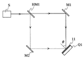
以下に、本発明の第1の実施形態に係る反射防止構造体を有する部材の製造方法について説明する。図1は、実施の形態1にかかる反射防止構造体を有する部材の製造方法において使用されるホログラム露光装置の構成図である。図1において、ホログラム露光装置は、レーザとレンズなどから構成される平行光線を出射する光源Sと、ハーフミラーHM1と、反射ミラーM1とM2とを備える。
(Embodiment 1)
Below, the manufacturing method of the member which has the reflection preventing structure which concerns on the 1st Embodiment of this invention is demonstrated. FIG. 1 is a configuration diagram of a hologram exposure apparatus used in a method for manufacturing a member having an antireflection structure according to a first embodiment. In FIG. 1, the hologram exposure apparatus includes a light source S that emits parallel light rays including a laser and a lens, a half mirror HM1, and reflection mirrors M1 and M2.
光源Sから放射された平行光はハーフミラーHM1に入射し、入射した光束はほぼ1対1に分割される。ハーフミラーHM1を透過した第1の光束(実線で表示)は、ミラーM1により反射されて、基板Q1上に形成されたフォトレジスト11に導かれる。一方、ハーフミラーHM1を反射した第2の光束(破線で表示)は、ミラーM2により反射されて、同じように基板Q1上に形成されたフォトレジスト11に導かれる。このとき、第1の光束のハーフミラーHM1を透過した光と、第2の光束のハーフミラーHM1から反射した光が基板Q1上で同じ入射角度θで重ね合わせたとき、基板Q1上に形成されたフォトレジスト11上にピッチがλ/(2×sinθ)のL/Sパターンである干渉縞パターンが形成される。(λは波長である)
The parallel light emitted from the light source S is incident on the half mirror HM1, and the incident light beam is split substantially in a one-to-one relationship. The first light beam (shown by a solid line) that has passed through the half mirror HM1 is reflected by the mirror M1 and guided to the
図2(A)、(B)および(C)は、実施の形態1において光束干渉により生成されるL/Sパターンを表す正面図である。図2(A)は、最初の露光に使用されるL/Sパターンを示し、図2(B)は、2回目の露光に使用されるL/Sパターンを示し、図2(C)は、3回目の露光に使用されるL/Sパターンを示す。L/Sパターンは、二光束干渉により生成される干渉縞であり、光束が干渉して強度を強め合う部分1と、光束が干渉して強度を弱め合う部分2を表している。
2A, 2B, and 2C are front views showing L / S patterns generated by light beam interference in the first embodiment. 2A shows an L / S pattern used for the first exposure, FIG. 2B shows an L / S pattern used for the second exposure, and FIG. The L / S pattern used for the third exposure is shown. The L / S pattern is an interference fringe generated by two-beam interference, and represents a
実施の形態1にかかる反射防止構造体を有する部材の製造方法は、L/Sパターン同士が互いに60度の角度をなすように、それぞれ光束を露光することにより、基板上に3つのパターンを重畳した光束の強度分布を形成する。すなわち、この部材の製造方法は、はじめにL/Sパターンを図2(A)の配置で露光した後、基板を右方向に60度回転させて図2(B)の配置で露光し、さらに、基板を右方向に60度回転させて図2(C)の配置で露光することに特徴を持っている。 In the method for manufacturing a member having an antireflection structure according to the first embodiment, three patterns are superimposed on a substrate by exposing light beams so that L / S patterns form an angle of 60 degrees with each other. The intensity distribution of the light flux is formed. That is, in the manufacturing method of this member, after the L / S pattern is first exposed in the arrangement of FIG. 2 (A), the substrate is rotated 60 degrees clockwise and exposed in the arrangement of FIG. 2 (B). It is characterized in that the substrate is rotated 60 degrees to the right and exposed in the arrangement shown in FIG.
図3(A)は、実施の形態1にかかる反射防止構造体を有する部材の製造方法において、露光後の基板上に形成される光束の強度分布を示す模式図である。また、図3(B)は、実施の形態1にかかる反射防止構造体を有する部材の製造方法において、露光後の基板上に照射された光束の強度分布を立体的に示した斜視拡大図である。 FIG. 3A is a schematic diagram illustrating the intensity distribution of a light beam formed on the substrate after exposure in the method for manufacturing a member having the antireflection structure according to the first embodiment. FIG. 3B is an enlarged perspective view showing the intensity distribution of the light beam irradiated on the substrate after exposure in a three-dimensional manner in the method for manufacturing the member having the antireflection structure according to the first embodiment. is there.
以下、実施の形態1の原理を説明する。露光は、図2(A)のL/Sパターンにより行われた後、基板Q1をL/Sパターンの強度分布において二光束が強め合う部分1と弱め合う部分2との境界部分において基板の法線方向を軸として60度回転させて、図2(B)の配置にして行われ、さらに、基板Q1をL/Sパターンの強め合う部分1と弱め合う部分2との境界部分において基板の法線方向を軸として60度回転させて、図2(C)の配置にして行われる。このように露光すると、L/Sパターンが光束の強め合う部分1と弱め合う部分2との幅が1対1になるよう形成されているので、3つのL/Sパターンが60度の角度をなす状態に重畳された三角格子パターンが基板上に照射される。
Hereinafter, the principle of the first embodiment will be described. After the exposure is performed using the L / S pattern of FIG. 2A, the substrate Q1 is subjected to the substrate method at the boundary portion between the
基板上に露光されるパターンは、図3(A)に示すように、露光量が4レベルの三角格子である。すなわち、露光後の基板上には、最小の露光量の領域(図3(A)中、「0」と記す)と、1回だけ光束が露光された領域(図3(A)中、「1」と記す)と、2回だけ光束が露光された領域(図3(A)中、「2」と記す)と、最大の露光量の領域(図3(A)中、「3」と記す)と、が形成される。これによって、従来の2回重ね合わせで形成される3レベルの形状の時に存在する中間的な領域(図10(A)の「1」)がなくなりほとんどの部分が急激な傾斜角を持つ斜めの領域となる。 As shown in FIG. 3A, the pattern exposed on the substrate is a triangular lattice with an exposure amount of 4 levels. That is, on the substrate after exposure, a region with the minimum exposure amount (denoted as “0” in FIG. 3A) and a region where the light beam is exposed only once (in FIG. 3A, “ 1 ”), a region where the light beam is exposed only twice (indicated as“ 2 ”in FIG. 3A), and a region with the maximum exposure amount (in FIG. 3A,“ 3 ”). To be formed). As a result, the intermediate region (“1” in FIG. 10A) existing at the time of the three-level shape formed by the conventional two-time superposition is eliminated, and most of the portions are slanted with a steep inclination angle. It becomes an area.
このように露光された基板を現像すると、光束が露光された領域は、すべて現像により凹部となる。このとき、凹部の形成深さは、照射される光束の強度が多いと深くなる。したがって、凹部は、いずれも光束が露光された領域、2回だけ光束が露光された領域、1回だけ光束が露光された領域の順に、深くなる。以上のようにして、図3(B)に示す4レベルの単位構造が周期的に形成された形状に対応する光束の強度分布の反転形状となる反射防止構造体を得ることができる。この構造は、4レベルの単位構造が反射率を低減すべき光の波長以下のピッチでアレイ状に配列されており、表面に入射する反射防止効果を奏する。 When the substrate exposed in this way is developed, the entire area where the light beam is exposed becomes a recess by development. At this time, the formation depth of the concave portion becomes deep when the intensity of the irradiated light beam is large. Accordingly, the recesses become deeper in the order of the region where the light beam is exposed, the region where the light beam is exposed only once, and the region where the light beam is exposed only once. As described above, it is possible to obtain an antireflection structure having an inverted shape of the intensity distribution of the light beam corresponding to the shape in which the four-level unit structure shown in FIG. 3B is periodically formed. In this structure, four-level unit structures are arranged in an array with a pitch equal to or less than the wavelength of light whose reflectance is to be reduced, and an antireflection effect of being incident on the surface is achieved.
以下、以上説明した実施の形態1にかかる反射防止構造体を有する部材の製造方法を具体的に説明する。図4は、実施の形態1にかかる反射防止構造体を有する部材の製造方法を説明する模式図である。
Hereinafter, the manufacturing method of the member which has the reflection preventing
石英ガラスを材料とする直径15mm、曲率半径40mm、厚み5mmを持つ平凸レンズを研削加工で高精度に加工し、石英ガラス基板Q1とした。この基板Q1は、表面を中心線表面粗さRa=2nm程度まで研磨加工されている。この石英ガラス基板Q1の表面に、スピンコート法を用いてフォトレジスト11を0.5μmの厚みで形成し、図1に示した装置を用いて、KrFレーザを光源として、波長248nmの紫外線の入射角度を30度として、二光束干渉によるホログラム露光を行い、照度7.7mW/cm2 で5秒間露光を行った(第1の露光工程:図4(A))。
A plano-convex lens having a diameter of 15 mm, a curvature radius of 40 mm, and a thickness of 5 mm made of quartz glass is processed with high precision by grinding to obtain a quartz glass substrate Q1. The substrate Q1 has a surface polished to a centerline surface roughness Ra of about 2 nm. A
次に、石英ガラス基板Q1を、曲面の頂点の法線方向を軸として回転させ、L/Sパターンが回転の前後で60度の角度をなすようにして、同様に図1に示した装置を用いてホログラム露光を行った(第2の露光工程:図4(B))。このホログラム露光の時間は、照度7.7mW/cm2 で5秒間である。さらに、石英ガラス基板Q1を、再び曲面の頂点の法線方向を軸として回転させ、L/Sパターンが回転の前後で60度の角度をなすようにして、ホログラム露光を行った(第2の露光工程:図4(C))。このホログラム露光の時間は、照度7.7mW/cm2 で5秒間である。 Next, the quartz glass substrate Q1 is rotated about the normal direction of the apex of the curved surface as an axis so that the L / S pattern forms an angle of 60 degrees before and after the rotation, and similarly the apparatus shown in FIG. Using this, hologram exposure was performed (second exposure step: FIG. 4B). The hologram exposure time is 5 seconds at an illuminance of 7.7 mW / cm 2 . Further, the quartz glass substrate Q1 was rotated again about the normal direction of the apex of the curved surface as an axis, and the hologram exposure was performed so that the L / S pattern formed an angle of 60 degrees before and after the rotation (second phase) Exposure process: FIG. 4 (C)). The hologram exposure time is 5 seconds at an illuminance of 7.7 mW / cm 2 .
露光の後、石英ガラス基板Q1をアルカリ現像液に1分間無攪拌浸漬してポストベーキング処理を施し、フォトレジスト11を、図3(B)に示す形状の反転構造を持つ高さ480nm、ピッチ240nmの微細形状13に加工した(現像工程:図4(D))。その後、微細形状13が形成された石英ガラス基板Q1をRFドライエッチング装置の中に入れ、CHF3 +O2 ガスを用いて、石英ガラス基板Q1表面をエッチング処理し、図3(B)に示す形状の反転形状である高さ240nmの三角錐に近い形状を持つ構造単位がピッチ240nmで配置された反射防止構造体15を持つ石英ガラス基板16を形成した(構造形成工程:図4(E))。従って、アスペクト比が1である反射防止構造体15が石英ガラス基板16の表面に形成された。この場合、フォトレジスト11と石英ガラスQ1のエッチングレート比は2:1であった。反射防止構造体15が形成された石英ガラス基板16の表面の反射率を測定したところ、波長が250nm以上の光について平均で約0.15%の値を示した。
After the exposure, the quartz glass substrate Q1 is immersed in an alkali developer for 1 minute without stirring and subjected to a post-baking treatment, and the
以上、説明したように、実施の形態1にかかる反射防止構造体の製造方法は、二光束干渉によるホログラム露光を行ってパターニングを行う際に、二光束干渉の結果生成されるL/Sパターンを3回露光するため、形成される反射防止構造体に平面部分が少なく、反射防止効果の高い構造を得ることができる。また、実施の形態1にかかる反射防止構造体の製造方法は、高精度の製造が必要であり高価なフォトマスクを用いないので、非常に安価で大面積の反射防止構造体を製造することができる。 As described above, in the manufacturing method of the antireflection structure according to the first embodiment, the L / S pattern generated as a result of the two-beam interference is used when patterning is performed by performing hologram exposure using two-beam interference. Since the exposure is performed three times, the formed antireflection structure has a small number of flat portions, and a structure having a high antireflection effect can be obtained. In addition, since the manufacturing method of the antireflection structure according to the first embodiment requires high-precision manufacturing and does not use an expensive photomask, it is possible to manufacture an antireflection structure having a very low cost and a large area. it can.
実施の形態1では、基板を60度回転させて露光し、さらに基板を60度回転させて露光して、L/Sパターンを重畳する例を示したがこれに限られない。例えば、基板を120度回転させて露光し、さらに120度回転させて露光して、L/Sパターンを重畳したり、基板を60度回転させて露光し、さらに逆方向に120度回転させて露光して、L/Sパターンを重畳したり、基板を120度回転させて露光し、さらに逆方向に60度回転させて露光して、L/Sパターンを重畳するなどしてもよい。要は、最終的に、L/Sパターン同士がそれぞれ60度の角度をなす関係になるように基板を回転させればよい。また、基板を回転させる代わりにホログラム露光の装置の光束照射部分を可動にして、L/Sパターンが回転するように構成してもよい。 In the first embodiment, an example is shown in which the substrate is rotated by 60 degrees for exposure, the substrate is further rotated by 60 degrees, and the L / S pattern is superimposed. However, the present invention is not limited to this. For example, the exposure is performed by rotating the substrate by 120 degrees, the rotation is further rotated by 120 degrees, the L / S pattern is superimposed, the exposure is performed by rotating the substrate by 60 degrees, and the rotation is further rotated by 120 degrees in the reverse direction. Exposure may be performed to superimpose an L / S pattern, or exposure may be performed by rotating the substrate by 120 degrees, and exposure may be performed by rotating the substrate by 60 degrees in the opposite direction, and the L / S pattern may be superimposed. In short, the substrate may be finally rotated so that the L / S patterns form an angle of 60 degrees with each other. Further, instead of rotating the substrate, the light beam irradiation portion of the hologram exposure apparatus may be made movable so that the L / S pattern rotates.
また、基板を45度ずつ回転させたり、30度ずつ回転させれば、更に、露光量のレベルを小刻みに変化させることができるようになり、より、反射防止効果を高めることは言うまでもない。すなわち、上記の実施の形態1では、回転後に露光されるべきL/Sパターンが、第1の露光工程において露光されたL/Sパターンとそれぞれ60度の角度をなす関係にあるときにそれぞれ露光する場合を示したが、これに限られず、さらに一般化して複数回の露光を行ってもよい。 Further, if the substrate is rotated by 45 degrees or rotated by 30 degrees, the exposure level can be changed in small increments, and it goes without saying that the antireflection effect is further improved. That is, in the first embodiment, the L / S pattern to be exposed after the rotation is exposed when the L / S pattern exposed in the first exposure step has an angle of 60 degrees. However, the present invention is not limited to this, and the exposure may be performed a plurality of times by further generalization.
例として、第2の露光工程が、n回(n=2,3,4・・・)の回転露光工程を含むとき、干渉縞パターンと基板とが以下の関係式を満足する位置でそれぞれ基板を露光する。
θi={180/(n+1)}*i
ただし、
i:1以上n以下の整数、
θi:回転後の干渉縞パターンが、前記第1の露光工程において露光された前記干渉縞パターンとなす角であって、小さい順にi番目のなす角、
である。
As an example, when the second exposure process includes n (n = 2, 3, 4...) Rotational exposure processes, the interference fringe pattern and the substrate each satisfy the following relational expression. To expose.
θi = {180 / (n + 1)} * i
However,
i: an integer from 1 to n,
θi: the angle formed by the interference fringe pattern after rotation with the interference fringe pattern exposed in the first exposure step, the i-th angle formed in ascending order,
It is.
上記関係式を満足する位置でそれぞれ基板を露光することにより、(n+1)レベルの段差を持つ形状を得るための光束の強度分布を形成することが可能である。このため、露光回数を増やすほど側面の傾斜が急で、アスペクト比が大きい3次元形状を得ることができるが、その分だけ製造工程が複雑になるので、反射防止構造体の性能と製造の容易さのバランスをみて回数を決定すればよい。 By exposing the substrate at a position satisfying the above relational expression, it is possible to form an intensity distribution of a light beam for obtaining a shape having a level difference of (n + 1) levels. For this reason, as the number of exposures increases, the side slope becomes steeper and a three-dimensional shape with a large aspect ratio can be obtained. However, the manufacturing process is complicated by that amount, and the performance and manufacturing of the antireflection structure are easy. The number of times may be determined in view of the balance.
露光は、干渉縞パターンと基板とがそれぞれ上記関係式を満足する位置で行えばよく、その関係にするプロセスは問わないことはいうまでもない。したがって、露光の間に行われる回転の方向や角度は適宜定めればよい。なお、実施の形態1において説明した3回露光は、上記関係式において、n=2である場合に相当する。 The exposure may be performed at a position where the interference fringe pattern and the substrate each satisfy the above relational expression, and it goes without saying that the process for making the relation does not matter. Therefore, the direction and angle of rotation performed during exposure may be determined as appropriate. Note that the three-time exposure described in the first embodiment corresponds to the case where n = 2 in the above relational expression.
(実施の形態2)
続いて、更に反射防止効果を高めるための具体例を、図5を用いて説明する。図5は、実施の形態2にかかる反射防止構造体を有する部材の製造方法を説明する模式図である
(Embodiment 2)
Next, a specific example for further enhancing the antireflection effect will be described with reference to FIG. FIG. 5 is a schematic diagram illustrating a method for manufacturing a member having an antireflection structure according to the second embodiment.
石英ガラスを材料とする直径15mm、曲率半径40mm、厚み5mmを持つ平凸レンズを研削加工で高精度に加工し、石英ガラス基板Q1とした。この基板Q1は、表面を中心線表面粗さRa=2nm程度まで研磨加工されている。この石英ガラス基板Q1の表面に、スパッタリング法を用いてエッチングマスクであるCr膜12を0.1μmの厚みで形成した。さらに、Cr膜12の上に、スピンコート法を用いてフォトレジスト11を0.5μmの厚みで形成し、図1に示した装置を用いて、KrFレーザを光源として、波長 248 nmの紫外線の入射角度を30度として、二光束干渉によるホログラム露光を行い、照度7.7mW/cm2 で5秒間露光を行った(第1の露光工程:図5(A))。
A plano-convex lens having a diameter of 15 mm, a curvature radius of 40 mm, and a thickness of 5 mm made of quartz glass is processed with high precision by grinding to obtain a quartz glass substrate Q1. The substrate Q1 has a surface polished to a centerline surface roughness Ra of about 2 nm. On the surface of this quartz glass substrate Q1, a
次に、石英ガラス基板Q1を、曲面の頂点の法線方向を軸として回転させ、L/Sパターンが回転の前後で60度の角度をなすようにして、同様に図1に示した装置を用いてホログラム露光を行った(第2の露光工程:図5(B))。このホログラム露光の時間は、照度7.7mW/cm2 で5秒間である。さらに、石英ガラス基板Q1を、再び曲面の頂点の法線方向を軸として回転させ、L/Sパターンが回転の前後で60度の角度をなすようにして、ホログラム露光を行った(第2の露光工程:図5(C))。このホログラム露光の時間は、照度7.7mW/cm2 で5秒間である。 Next, the quartz glass substrate Q1 is rotated about the normal direction of the apex of the curved surface as an axis so that the L / S pattern forms an angle of 60 degrees before and after the rotation, and similarly the apparatus shown in FIG. Using this, hologram exposure was performed (second exposure step: FIG. 5B). The hologram exposure time is 5 seconds at an illuminance of 7.7 mW / cm 2 . Further, the quartz glass substrate Q1 was rotated again about the normal direction of the apex of the curved surface as an axis, and the hologram exposure was performed so that the L / S pattern formed an angle of 60 degrees before and after the rotation (second phase) Exposure process: FIG. 5 (C)). The hologram exposure time is 5 seconds at an illuminance of 7.7 mW / cm 2 .
露光の後、石英ガラス基板Q1をアルカリ現像液に1分間無攪拌浸漬してポストベーキング処理を施し、フォトレジスト11を、図3(B)に示す形状の反転構造を持つ高さ480nm、ピッチ240nmの微細形状13に加工した(現像工程:図5(D))。その後、微細形状13をマスクとしてArガスを用いたイオンミリング装置によって、ドライエッチング処理することにより、Crからなる微細形状14をエッチングマスクとして形成した(構造形成工程:図5(E))。この時、微細形状14は高さ80nm、ピッチ240nmであった。従って、この場合、フォトレジスト11とCr膜12のエッチングレート比は6:1であった。最後に、微細形状14が形成された石英ガラス基板Q1をRFドライエッチング装置の中に入れ、CHF3 +O2 ガスを用いて、石英ガラス基板Q1表面をエッチング処理し、高さ480nmの三角錐に近い形状を持つ構造単位がピッチ240nmで配置された反射防止構造体15を持つ石英ガラス基板16を形成した(構造形成工程:図5(F))。この場合、Cr膜12と石英ガラス基板Q1のエッチングレート比は1:6であった。従って、アスペクト比が2である反射防止構造体15が石英ガラス基板16の表面に形成された。この時の、石英ガラス基板16の表面の反射率を測定したところ、波長が250nm以上の光について平均で約0.07%の値を示した。
After the exposure, the quartz glass substrate Q1 is immersed in an alkali developer for 1 minute without stirring and subjected to a post-baking process, and the
なお、エッチングマスクの材料として、具体的にCr膜を挙げたがこれに限られない。石英などの最終部材とのエッチングにおける選択比が大きい材料であればよい。例えば、エッチングマスクが、Cr、Ni、Al、C、Ta、Mo、Fe、Pt、Au等のいずれの膜であってもよい。 In addition, although the Cr film was specifically mentioned as an etching mask material, it is not restricted to this. Any material that has a high selectivity in etching with the final member such as quartz may be used. For example, the etching mask may be any film such as Cr, Ni, Al, C, Ta, Mo, Fe, Pt, or Au.
以上、説明したように、実施の形態2にかかる反射防止構造体の製造方法は、二光束干渉によるホログラム露光を行ってパターニングを行う際に、二光束干渉の結果生成されるL/Sパターンを3回露光するため、形成される反射防止構造体に平面部分が少なく、反射防止効果の高い構造を得ることができる。また、実施の形態2にかかる反射防止構造体の製造方法は、高精度の製造が必要であり高価なフォトマスクを用いないので、非常に安価で大面積の反射防止構造体を製造することができる。 As described above, in the method for manufacturing the antireflection structure according to the second embodiment, the L / S pattern generated as a result of two-beam interference is used when patterning is performed by performing hologram exposure using two-beam interference. Since the exposure is performed three times, the formed antireflection structure has a small number of flat portions, and a structure having a high antireflection effect can be obtained. In addition, since the manufacturing method of the antireflection structure according to the second embodiment requires high-precision manufacturing and does not use an expensive photomask, it is possible to manufacture an antireflection structure having a very low cost and a large area. it can.
実施の形態2では、基板を60度回転させて露光し、さらに基板を60度回転させて露光して、L/Sパターンを重畳する例を示したがこれに限られない。例えば、基板を120度回転させて露光し、さらに120度回転させて露光して、L/Sパターンを重畳したり、基板を60度回転させて露光し、さらに逆方向に120度回転させて露光して、L/Sパターンを重畳したり、基板を120度回転させて露光し、さらに逆方向に60度回転させて露光して、L/Sパターンを重畳するなどしてもよい。要は、最終的に、L/Sパターン同士がそれぞれ60度の角度をなす関係になるように基板を回転させればよい。また、基板を回転させる代わりにホログラム露光の装置の光束照射部分を可動にして、L/Sパターンが回転するように構成してもよい。 In the second embodiment, the example in which the exposure is performed by rotating the substrate by 60 degrees, the exposure is performed by rotating the substrate by 60 degrees, and the L / S pattern is superimposed is shown, but the present invention is not limited thereto. For example, the exposure is performed by rotating the substrate by 120 degrees, the rotation is further rotated by 120 degrees, the L / S pattern is superimposed, the exposure is performed by rotating the substrate by 60 degrees, and the rotation is further rotated by 120 degrees in the reverse direction. Exposure may be performed to superimpose an L / S pattern, or exposure may be performed by rotating the substrate by 120 degrees, and exposure may be performed by rotating the substrate by 60 degrees in the opposite direction, and the L / S pattern may be superimposed. In short, the substrate may be finally rotated so that the L / S patterns form an angle of 60 degrees with each other. Further, instead of rotating the substrate, the light beam irradiation portion of the hologram exposure apparatus may be made movable so that the L / S pattern rotates.
また、回転角度を45度ずつ回転させたり、30度ずつ回転させれば、更に、露光量のレベルを小刻みに変化させることができるようになり、より、反射防止効果を高めることは言うまでもない。すなわち、上記の実施の形態2では、回転後に露光されるべきL/Sパターンが、第1の露光工程において露光されたL/Sパターンとそれぞれ60度の角度をなす関係にあるときにそれぞれ露光する場合を示したが、これに限られず、さらに一般化して複数回の露光を行ってもよい。 Further, if the rotation angle is rotated by 45 degrees or 30 degrees, the exposure level can be changed in small increments, and it goes without saying that the antireflection effect is further enhanced. That is, in the above-described second embodiment, the exposure is performed when the L / S pattern to be exposed after the rotation has a relationship of 60 degrees with the L / S pattern exposed in the first exposure step. However, the present invention is not limited to this, and the exposure may be performed a plurality of times by further generalization.
例として、第2の露光工程が、n回(n=2,3,4・・・)の回転露光工程を含むとき、干渉縞パターンと基板とが以下の関係式を満足する位置でそれぞれ基板を露光する。
θi={180/(n+1)}*i
ただし、
i:1以上n以下の整数、
θi:回転後の干渉縞パターンが、前記第1の露光工程において露光された前記干渉縞パターンとなす角であって、小さい順にi番目のなす角、
である。
As an example, when the second exposure process includes n (n = 2, 3, 4...) Rotational exposure processes, the interference fringe pattern and the substrate each satisfy the following relational expression. To expose.
θi = {180 / (n + 1)} * i
However,
i: an integer from 1 to n,
θi: the angle formed by the interference fringe pattern after rotation with the interference fringe pattern exposed in the first exposure step, the i-th angle formed in ascending order,
It is.
上記関係式を満足する位置でそれぞれ基板を露光することにより、(n+1)レベルの段差を持つ形状を得るための光束の強度分布を形成することが可能である。このため、露光回数を増やすほど側面の傾斜が急で、アスペクト比が大きい3次元形状を得ることができるが、その分だけ製造工程が複雑になるので、反射防止構造体の性能と製造の容易さのバランスをみて回数を決定すればよい。 By exposing the substrate at a position satisfying the above relational expression, it is possible to form an intensity distribution of a light beam for obtaining a shape having a level difference of (n + 1) levels. For this reason, as the number of exposures increases, the side slope becomes steeper and a three-dimensional shape with a large aspect ratio can be obtained. However, the manufacturing process is complicated by that amount, and the performance and manufacturing of the antireflection structure are easy. The number of times may be determined in view of the balance.
露光は、干渉縞パターンと基板とがそれぞれ上記関係式を満足する位置で行えばよく、その関係にするプロセスは問わないことはいうまでもない。したがって、露光の間に行われる回転の方向や角度は適宜定めればよい。なお、実施の形態2において説明した3回露光は、上記関係式において、n=2である場合に相当する。 The exposure may be performed at a position where the interference fringe pattern and the substrate each satisfy the above relational expression, and it goes without saying that the process for making the relation does not matter. Therefore, the direction and angle of rotation performed during exposure may be determined as appropriate. Note that the three-time exposure described in the second embodiment corresponds to the case where n = 2 in the above relational expression.
(実施の形態3)
本実施形態では、第1あるいは第2の実施形態に係る方法により作成された反射防止構造体を有する部材を用いて、電鋳処理により複製型を製造する方法について説明する。図6は、実施の形態3にかかる反射防止構造体を有する部材の製造方法に用いる電鋳型の製造方法を説明する模式図である。実施の形態3にかかる反射防止構造体を有する部材の製造方法は、型を電鋳複製することを特徴としている。以下、実施の形態1の製造方法により作成された反射防止構造体が形成された石英ガラス基板16を電鋳複製するプロセスを例に説明を行う。
(Embodiment 3)
In the present embodiment, a method for manufacturing a replica mold by electroforming using a member having an antireflection structure produced by the method according to the first or second embodiment will be described. FIG. 6 is a schematic diagram for explaining a method for producing an electroforming mold used in a method for producing a member having an antireflection structure according to the third embodiment. The method for manufacturing a member having an antireflection structure according to the third embodiment is characterized in that the mold is electroformed and duplicated. Hereinafter, a process of electroforming and duplicating the
はじめに、実施の形態1において説明したものと同様の製造方法により製造された反射防止構造体62を有する石英ガラスからなるレンズ原盤61を準備した(図6(A))。まず、石英ガラスからなるレンズ原盤61は、導電性ではないので、増感処理を行った後、Pdによる活性化処理を行った後、無電解メッキ用Ni/B溶液63に浸漬して、反射防止構造体62の表面に無電解メッキ層64を形成した(図6(B))。石英ガラスからなるレンズ原盤61の反射防止構造体62に形成された無電解Ni/Bメッキ層64は、40nmの厚みを有していた。
First, a lens master 61 made of quartz glass having an
続いて、無電解メッキ層64を形成した石英ガラスからなるレンズ原盤61をスルファミン酸ニッケル電解液65に浸漬し、電気メッキを行って石英ガラスからなるレンズ原盤61の表面にNiメッキ層66を形成させた(図6(C))。その後、Niメッキした石英ガラスからなるレンズ原盤61をメッキ液から取り出し(図6(D))、石英ガラスからなるレンズ原盤61からNi複製型68を機械的に引き離した(図6(E))。Ni複製型68の厚さは4.0mmであった。
Subsequently, the lens master 61 made of quartz glass on which the
以上のように複製された型は、加熱軟化された樹脂やガラス等を直接成形する型として用いることができる。実施の形態3によれば、反射防止構造体を成形するために用いる型を電子ビーム描画などの高コストで生産性の低い方法によらずに製造することが可能になる。 The mold replicated as described above can be used as a mold for directly molding a heat-softened resin or glass. According to the third embodiment, it is possible to manufacture a mold used for molding the antireflection structure without using a high-cost and low-productivity method such as electron beam drawing.
(実施の形態4)
本実施形態では、第1あるいは第2の実施形態に係る方法により反射防止構造体が形成された部材を成形型として用い、プレス成形により、表面に反射防止構造体が形成された部材を製造する方法について説明する。
(Embodiment 4)
In the present embodiment, a member having an antireflection structure formed on the surface is manufactured by press molding using a member having the antireflection structure formed by the method according to the first or second embodiment as a mold. A method will be described.
図7(A)は、プレス成形を行う成形機の構成を示す断面図である。図7(A)において、チャンバー76は、その内部を全て窒素(N2 )ガスに置換されており、上型72と下型73とが対向して配置されている。上型72は、第2の実施形態に係る製造方法により反射防止構造体が形成された石英ガラスからなる凹レンズであり、図示されていない駆動軸によって上下可動に構成されている。下型73は、炭化タングステン(WC)を主成分とした材料からなり、レンズの成形材料を保持できるように凹部が成形されている。そして、上型72の成形面および下型73の凹部には、離型性の向上を図るために、離型膜71が形成されている。離型膜71は、スパッタリング法により形成されたIr−Rh合金薄膜であり、上型72に形成された離型膜71の厚みは0.01μmであり、下型73に形成された離型膜71の厚みは0.03μmである。
FIG. 7A is a cross-sectional view illustrating a configuration of a molding machine that performs press molding. In FIG. 7A, the interior of the
下型73の凹部には、レンズの成形材料となるガラス基板74が載置されている。ガラス基板74は、クラウン系硼珪酸ガラス(転移点Tg:501°C、屈伏点At:549°C)からなり、その表面には、窒化硼素(BN)を主成分とする離型剤75が形成されている。
A
図7(B)は、ガラス基板74にプレス加工を行う状態を示す。図7(B)において、上型72は下降して、ガラス基板74を590℃、1000Nの条件下で3分間プレス成形する。プレス加工が終了すると、冷却処理を行うことなく、図7(C)に示すように、上型72を上昇させる。これにより、成形されたガラスレンズ74の表面には、上型72に形成された反射防止構造体とは反転形状を有する反射防止構造体が形成される。
FIG. 7B shows a state where the
図7(D)は、チャンバー76内から取り出したレンズ77を示す断面図である。レンズ77の表面反射率を測定したところ、波長が250nm以上の光について平均で約0.07%の値を示した。なお、表面保護の薄膜がなければ、ガラス材料は部分的に直接型に接触し、融着を起こして型から離型させることができなくなってしまう。無理に離型しようとすると、ガラス材料あるいは型が割れてしまう。
FIG. 7D is a cross-sectional view showing the
以上のように、実施の形態4によれば、実施の形態1あるいは2に示した方法で作製した部材を型として、加熱軟化された樹脂やガラス等を直接成形して、反射防止構造体を有する光学素子などの部材を、非常に安価に容易に、そして、大量生産する事を可能としたものである。 As described above, according to the fourth embodiment, an antireflection structure is formed by directly molding a heat-softened resin or glass using the member produced by the method shown in the first or second embodiment as a mold. It is possible to easily and mass-produce a member such as an optical element having a very low cost.
(実施の形態5)
次に、図8を参照して、反射防止構造体を有する部材を製造する別の方法を説明する。図8は、実施の形態5にかかる反射防止構造体を有する部材の製造方法を説明する模式図である。実施の形態5は、実施の形態3で説明した方法で作製した電鋳複製された型を用いて光学樹脂からなる部材を成形することを特徴としている。
(Embodiment 5)
Next, another method for manufacturing a member having an antireflection structure will be described with reference to FIG. FIG. 8 is a schematic diagram illustrating a method for manufacturing a member having an antireflection structure according to the fifth embodiment. The fifth embodiment is characterized in that a member made of an optical resin is molded using an electroformed and duplicated mold manufactured by the method described in the third embodiment.
先に説明した電鋳型83をインサート型として、ベース型81に組み込み、樹脂が充填されるキャビティ内面全体にシランカップリング剤を塗布して、表面保護離型層82を形成した(図8(A))。次に、電鋳型83を80°Cに加熱し、流動状態にあるポリオレフィン樹脂84を型内に射出し(図8(B))、充填した(図8(C))。樹脂が冷却により固化したら、型を開き樹脂を取り出し、反射防止構造体が形成された樹脂85を得た。反射防止構造体が形成された樹脂85の表面の反射率を測定したところ、波長が250nm以上の光について平均で約0.15%の値を示した。なお、本実施の形態はアクリル、テフロン(登録商標)、ポリエチレン、ポリオレフィンなどが樹脂材料として用いることができる。
The
(実施の形態6)
実施の形態6は、実施の形態3で説明した方法で作製した電鋳複製型を用いて光学樹脂かならなる部材を成形することを特徴としている。シランカップリング剤により表面保護膜を形成した電鋳複製型を用いて、実施の形態4と同様の成形機(図7)を用いて、光学樹脂材料をプレス成形した。表面保護膜を形成した電鋳複製型を上型とし、WCを主成分とする超硬合金を下型に用いた。上型、下型、及びPMMA樹脂基板をセットし、180°C、20MPaでプレス成形し、樹脂基板表面に反射防止構造体を形成した。反射防止構造体が形成された樹脂表面の反射率を測定したところ、波長が250nm以上の光について平均で約0.15%の値を示した。なお、本実施の形態はアクリル、テフロン(登録商標)、ポリエチレン、ポリオレフィンなどを樹脂基板として用いることができる。
(Embodiment 6)
The sixth embodiment is characterized in that a member made of an optical resin is molded using an electroformed replication mold produced by the method described in the third embodiment. The optical resin material was press-molded using the same molding machine (FIG. 7) as in Embodiment 4 using an electroformed replication mold in which a surface protective film was formed with a silane coupling agent. An electroformed replication mold having a surface protective film formed thereon was used as an upper mold, and a cemented carbide containing WC as a main component was used as a lower mold. The upper mold, the lower mold, and the PMMA resin substrate were set and press molded at 180 ° C. and 20 MPa to form an antireflection structure on the surface of the resin substrate. When the reflectance of the resin surface on which the antireflection structure was formed was measured, the average value of light having a wavelength of 250 nm or more was about 0.15%. In this embodiment mode, acrylic, Teflon (registered trademark), polyethylene, polyolefin, or the like can be used as the resin substrate.
本発明は、デジタルカメラやプリンタ装置などに用いられるレンズ素子、プリズム素子など光路中の光線に対する反射防止処理が必要な光学機能面を持つ光学素子に好適である。また、本発明は、それら光学素子の保持に用いられる構造部材や光学素子を含む機器全体を保護する筐体部材などに適用することにより、不要光を防止する反射防止面とすることができる。さらに、本発明は、半導体レーザ素子や発光ダイオードなどの発光素子や、フォトダイオードなどの受光素子、CCDやCMOSなどの撮像素子や、光通信に用いられる光スイッチや分岐器などの各種デバイスにおいて、反射防止処理が必要な部分に形成することにより、各デバイスの機能を向上させることができる。さらに、本発明は、液晶表示パネルや有機エレクトロルミネッセンスパネル、プラズマ発光パネルなどのディスプレイパネルの表示部分に適用してもよい。その他、本発明は、光学機器に用いられる反射防止処理が必要なあらゆる部材に対して広く適用可能である。 The present invention is suitable for an optical element having an optical function surface that requires antireflection processing for light rays in an optical path, such as a lens element and a prism element used in a digital camera, a printer device, and the like. In addition, the present invention can be applied to a structural member used for holding these optical elements or a casing member that protects the entire apparatus including the optical elements, thereby providing an antireflection surface that prevents unnecessary light. Furthermore, the present invention relates to various devices such as light emitting elements such as semiconductor laser elements and light emitting diodes, light receiving elements such as photodiodes, imaging elements such as CCD and CMOS, optical switches and branching devices used for optical communication, The function of each device can be improved by forming it in a portion requiring antireflection treatment. Furthermore, the present invention may be applied to a display portion of a display panel such as a liquid crystal display panel, an organic electroluminescence panel, or a plasma light emitting panel. In addition, the present invention can be widely applied to all members that require an antireflection treatment used in optical equipment.
Q1 基板
1 光束が干渉して強度を強め合う部分
2 光束が干渉して強度を弱め合う部分
11 フォトレジスト
12 Cr膜
13 微細形状
14 微細形状
15 反射防止構造体
16 石英ガラス基板
61 石英ガラスからなるレンズ原盤
62 反射防止構造体
63 Ni/B溶液
64 無電解メッキ層
65 スルファミン酸ニッケル電解液
66 Niメッキ層
68 Ni複製型
71 離型膜
72 上型
73 下型
74 成形用材料
75 離型剤
76 チャンバー
77 レンズ
81 ベース型
82 表面保護離型層
83 電鋳型
84 流動状態のポリオレフィン樹脂
85 樹脂
91 光束が干渉して強度を強め合う部分
92 光束が干渉して強度を弱め合う部分
Claims (7)
少なくとも構造体形成面が感光性材料からなる前記部材となる基板上に、直接、二本の光束を重ね合わせることにより形成される干渉縞パターンからなる光強度分布を生成し、当該基板を露光する第1の露光工程と、
前記基板上に生成される前記干渉縞パターンが、前記第1の露光工程において露光された前記干渉縞パターンとは所定角をなす関係になるように、前記基板と前記干渉縞パターンとの相対的な位置関係を変更した後、前記基板を露光する露光工程を、少なくとも2回含む第2の露光工程と、
露光された前記基板を現像する現像工程とを備える、反射防止構造体を有する部材の製造方法。 A method of manufacturing a member having an antireflection structure in which a predetermined shape is a structural unit, and the predetermined shape is arranged in an array at a pitch equal to or less than a wavelength of light whose reflectance is to be reduced,
A light intensity distribution composed of an interference fringe pattern formed by superimposing two light beams directly on a substrate that is a member having at least a structure forming surface made of a photosensitive material is generated, and the substrate is exposed. A first exposure step;
Relative relation between the substrate and the interference fringe pattern so that the interference fringe pattern generated on the substrate forms a predetermined angle with the interference fringe pattern exposed in the first exposure step. An exposure step of exposing the substrate after changing the positional relationship, a second exposure step including at least twice,
The manufacturing method of the member which has an antireflection structure provided with the image development process which develops the exposed substrate.
θi={180/(n+1)}*i
ただし、
i:1以上n以下の整数、
θi:回転後の前記干渉縞パターンが、前記第1の露光工程において露光された前記干渉縞パターンとなす角であって、小さい順にi番目のなす角、
である。 When the second exposure step includes n times (n = 2, 3, 4...) Of the exposure step, the interference fringe pattern and the substrate satisfy the following relational expressions, respectively. The manufacturing method of the member which has a reflection preventing structure of Claim 1 which exposes a board | substrate:
θi = {180 / (n + 1)} * i
However,
i: an integer from 1 to n,
θi: the angle formed by the interference fringe pattern after rotation with the interference fringe pattern exposed in the first exposure step, the angle formed by the i-th in ascending order,
It is.
前記現像工程の後に、当該現像工程によってパターン形成された前記感光性レジストをマスクとして前記部材をドライエッチングするエッチング工程をさらに備えることを特徴とする、請求項1に記載の反射防止構造体を有する部材の製造方法。 The photosensitive material is a photosensitive resist,
2. The antireflection structure according to claim 1, further comprising, after the developing step, an etching step of dry etching the member using the photosensitive resist patterned by the developing step as a mask. Manufacturing method of member.
前記現像工程の後に、当該現像工程によってパターン形成された前記感光性レジストをマスクとして、前記エッチングマスク層をウェットエッチングあるいはドライエッチングする第1のエッチング工程と、前記第1のエッチング工程によってパターン形成されたエッチングマスク層をマスクとして前記部材をドライエッチングする第2のエッチング工程とをさらに備えることを特徴とする、請求項1に記載の反射防止構造体を有する部材の製造方法。 The photosensitive material is a photosensitive resist, and has an etching mask layer made of a material for an etching mask under the layer made of the photosensitive resist.
After the development step, the etching resist layer is patterned by wet etching or dry etching using the photosensitive resist patterned by the development step as a mask, and by the first etching step. The method for manufacturing a member having an antireflection structure according to claim 1, further comprising a second etching step of dry etching the member using the etching mask layer as a mask.
Priority Applications (1)
| Application Number | Priority Date | Filing Date | Title |
|---|---|---|---|
| JP2005062474A JP2006243633A (en) | 2005-03-07 | 2005-03-07 | Manufacturing method of member having antireflection structure body |
Applications Claiming Priority (1)
| Application Number | Priority Date | Filing Date | Title |
|---|---|---|---|
| JP2005062474A JP2006243633A (en) | 2005-03-07 | 2005-03-07 | Manufacturing method of member having antireflection structure body |
Publications (2)
| Publication Number | Publication Date |
|---|---|
| JP2006243633A true JP2006243633A (en) | 2006-09-14 |
| JP2006243633A5 JP2006243633A5 (en) | 2007-12-27 |
Family
ID=37050067
Family Applications (1)
| Application Number | Title | Priority Date | Filing Date |
|---|---|---|---|
| JP2005062474A Pending JP2006243633A (en) | 2005-03-07 | 2005-03-07 | Manufacturing method of member having antireflection structure body |
Country Status (1)
| Country | Link |
|---|---|
| JP (1) | JP2006243633A (en) |
Cited By (5)
| Publication number | Priority date | Publication date | Assignee | Title |
|---|---|---|---|---|
| JP2009186227A (en) * | 2008-02-04 | 2009-08-20 | Seiko Epson Corp | Timepiece, light-transmitting member, and its manufacturing method |
| US8226837B2 (en) | 2006-11-15 | 2012-07-24 | National Institute Of Advanced Industrial Science And Technology | Mold for optical device with anti-reflection structure, method for producing the same, and optical device |
| WO2013084899A1 (en) * | 2011-12-08 | 2013-06-13 | 旭硝子株式会社 | Anti-reflection structure and method for manufacturing anti-reflection structure |
| CN105789485A (en) * | 2016-03-14 | 2016-07-20 | 淮阴工学院 | Fabrication method of holographic speckle structured organic light emitting diode |
| WO2021125207A1 (en) | 2019-12-17 | 2021-06-24 | 国立研究開発法人産業技術総合研究所 | Antireflection structure and method for manufacturing same |
Citations (5)
| Publication number | Priority date | Publication date | Assignee | Title |
|---|---|---|---|---|
| JPH09260255A (en) * | 1996-03-25 | 1997-10-03 | Nippon Telegr & Teleph Corp <Ntt> | Projection exposure method |
| JP2001272505A (en) * | 2000-03-24 | 2001-10-05 | Japan Science & Technology Corp | Surface treating method |
| JP2004205990A (en) * | 2002-12-26 | 2004-07-22 | Dainippon Printing Co Ltd | Manufacturing method of fine rugged pattern having antireflection performance and antireflection article |
| JP2004268331A (en) * | 2003-03-06 | 2004-09-30 | Minolta Co Ltd | Mold for molding optical element and method for manufacturing mold |
| JP2004317922A (en) * | 2003-04-18 | 2004-11-11 | Minolta Co Ltd | Surface processing method, optical element, and metal mold therefor |
-
2005
- 2005-03-07 JP JP2005062474A patent/JP2006243633A/en active Pending
Patent Citations (5)
| Publication number | Priority date | Publication date | Assignee | Title |
|---|---|---|---|---|
| JPH09260255A (en) * | 1996-03-25 | 1997-10-03 | Nippon Telegr & Teleph Corp <Ntt> | Projection exposure method |
| JP2001272505A (en) * | 2000-03-24 | 2001-10-05 | Japan Science & Technology Corp | Surface treating method |
| JP2004205990A (en) * | 2002-12-26 | 2004-07-22 | Dainippon Printing Co Ltd | Manufacturing method of fine rugged pattern having antireflection performance and antireflection article |
| JP2004268331A (en) * | 2003-03-06 | 2004-09-30 | Minolta Co Ltd | Mold for molding optical element and method for manufacturing mold |
| JP2004317922A (en) * | 2003-04-18 | 2004-11-11 | Minolta Co Ltd | Surface processing method, optical element, and metal mold therefor |
Cited By (5)
| Publication number | Priority date | Publication date | Assignee | Title |
|---|---|---|---|---|
| US8226837B2 (en) | 2006-11-15 | 2012-07-24 | National Institute Of Advanced Industrial Science And Technology | Mold for optical device with anti-reflection structure, method for producing the same, and optical device |
| JP2009186227A (en) * | 2008-02-04 | 2009-08-20 | Seiko Epson Corp | Timepiece, light-transmitting member, and its manufacturing method |
| WO2013084899A1 (en) * | 2011-12-08 | 2013-06-13 | 旭硝子株式会社 | Anti-reflection structure and method for manufacturing anti-reflection structure |
| CN105789485A (en) * | 2016-03-14 | 2016-07-20 | 淮阴工学院 | Fabrication method of holographic speckle structured organic light emitting diode |
| WO2021125207A1 (en) | 2019-12-17 | 2021-06-24 | 国立研究開発法人産業技術総合研究所 | Antireflection structure and method for manufacturing same |
Similar Documents
| Publication | Publication Date | Title |
|---|---|---|
| TW544673B (en) | Micro lens and method and apparatus for fabricating | |
| CN101268012B (en) | Fine structure body and method for manufacturing same | |
| CN101154035B (en) | Fine mold and method for regenerating fine mold | |
| US20040032667A1 (en) | Technique for microstructuring replication mold | |
| JP5081443B2 (en) | OPTICAL ELEMENT AND ITS MANUFACTURING METHOD, OPTICAL ELEMENT MANUFACTURING REPLICATION BOARD AND ITS MANUFACTURING METHOD | |
| JP2006251318A (en) | Manufacturing method of member having antireflective structure | |
| JP2006243633A (en) | Manufacturing method of member having antireflection structure body | |
| JP2006317807A (en) | Member equipped with antireflection structure and manufacturing method of the member | |
| JP2006235195A (en) | Method for manufacturing member with antireflective structure | |
| JP2009128539A (en) | Method for manufacturing antireflection structure | |
| JP2006171229A (en) | Nonreflective structure and optical element with nonreflective structure, and manufacturing method thereof and mask used for same | |
| JPH07174902A (en) | Microlens array and its production | |
| JP4594745B2 (en) | Method for manufacturing member having antireflection structure | |
| JP2011027867A (en) | Optical component, method of manufacturing the optical component, lens assembly and method of manufacturing the lens assembly | |
| JP4820871B2 (en) | Antireflection structure and manufacturing method thereof | |
| JP2009128541A (en) | Method for manufacturing antireflection structure | |
| JPH11160510A (en) | Manufacture of multistage staircase-like element and manufacture of mold for manufacturing the element | |
| JP2002287370A (en) | Method for manufacturing optical element | |
| JP2006305800A (en) | Mold and manufacturing method of resin molded product | |
| JP2006195289A (en) | Manufacturing method of optical element having nonreflection structure | |
| JP4463775B2 (en) | Mask for X-ray lithography, method for producing the same, method for producing an antireflection structure using the same, method for producing a mold for producing an optical element having an antireflection structure, and glass having an antireflection structure Manufacturing method of molded article or resin molded article | |
| JP4814938B2 (en) | Antireflection structure and manufacturing method thereof | |
| JP2020024243A (en) | Optical element with antireflection structure, method for manufacturing the same, method for manufacturing mold for manufacture, and imaging apparatus | |
| JP2009151257A (en) | Inclined exposure lithography system | |
| JP4262514B2 (en) | Manufacturing method of optical member |
Legal Events
| Date | Code | Title | Description |
|---|---|---|---|
| A521 | Written amendment |
Free format text: JAPANESE INTERMEDIATE CODE: A523 Effective date: 20071109 |
|
| A621 | Written request for application examination |
Free format text: JAPANESE INTERMEDIATE CODE: A621 Effective date: 20071109 |
|
| A977 | Report on retrieval |
Free format text: JAPANESE INTERMEDIATE CODE: A971007 Effective date: 20100603 |
|
| A131 | Notification of reasons for refusal |
Free format text: JAPANESE INTERMEDIATE CODE: A131 Effective date: 20100607 |
|
| A02 | Decision of refusal |
Free format text: JAPANESE INTERMEDIATE CODE: A02 Effective date: 20101013 |