JP2004268331A - Mold for molding optical element and method for manufacturing mold - Google Patents
Mold for molding optical element and method for manufacturing mold Download PDFInfo
- Publication number
- JP2004268331A JP2004268331A JP2003060235A JP2003060235A JP2004268331A JP 2004268331 A JP2004268331 A JP 2004268331A JP 2003060235 A JP2003060235 A JP 2003060235A JP 2003060235 A JP2003060235 A JP 2003060235A JP 2004268331 A JP2004268331 A JP 2004268331A
- Authority
- JP
- Japan
- Prior art keywords
- mold
- layer
- etching
- optical element
- lens
- Prior art date
- Legal status (The legal status is an assumption and is not a legal conclusion. Google has not performed a legal analysis and makes no representation as to the accuracy of the status listed.)
- Granted
Links
Images


Abstract
Description
【0001】
【発明の属する技術分野】
本発明は、光学素子用の金型に関するものであり、特に、曲面上に微細な構造を持つ光学素子を成型するための金型に関する。また、そのような金型の製造方法に関する。
【0002】
【従来の技術】
【特許文献1】
特開昭62−96902号公報
【特許文献2】
特開2000−182024号公報
【特許文献3】
特開2002−326231号公報
【特許文献4】
特開2002−274865号公報
【0003】
近年、CGH(Computer Generated Hologram)に代表されるような複雑な構造の回折格子や、蒸着膜によらないで反射防止を行うための微細構造を、光学素子例えばレンズ表面に形成することが求められている。例えば、CGHをレンズと一体化することで、レンズの持つ集光(結像)作用と、回折による別の作用とを1枚のレンズで実現できる。また、反射防止を行うための微細構造をレンズ面に形成すれば、より高性能な反射防止を行うことができる。つまり、これらの微細構造をレンズ面に形成することで、光学系の高機能化、小型化、高性能化を行うことができる。
【0004】
一方、このような光学素子を安価に大量に生産するために、金型を作製し、その金型形状を合成樹脂材料に転写することが行われている。この場合、金型にレンズ面の形状と、微細構造とを、加工する必要がある。このような形状の金型は、特許文献1、2および3に記載されている。
【0005】
特許文献1記載の金型は、反射防止構造をもつレンズ面を成型する金型であって、その表面には波長以下の深さの鋸状構造が形成されている。金型表面にアルゴンイオンビームで1/20波長の照射傷を形成し、これを硝酸水溶液で表面腐食させることで鋸状構造が形成される。
【0006】
特許文献2記載の金型は、同心円状をなす多数の微細なエレメントからなる回折光学面が形成されているレンズ用の金型である。機械加工によって曲面形状を形成した金型表面上に、フォトレジスト層を形成し、該レジスト層の表面に機械加工によって回折光学面を形成するとともにドライエッチングによって上記レジスト層が除去されるまでエッチング処理することによって作製されている。
【0007】
一方、必要とする素子形状をマスター型として作製し、そのマスター型の形状を電鋳により写し取り、金型とする方法も広く用いられている。
【0008】
【発明が解決しようとする課題】
しかしながら、特許文献1記載の金型は、アルゴンイオンビームで形成した照射傷を硝酸水溶液で腐食させて作製されているため、金型面全体に一様に広がる鋸形状を形成することはできるが、CGH等の複雑な構造の微細構造を高精度に形成することはできない。
【0009】
特許文献2記載の金型は、回折光学面を、フォトレジスト層上に機械加工によって形成しているが、このような加工法は1次元構造や軸対称構造なら作製可能であるが、CGH等のように2次元に多様で複雑な微細構造をもつ場合には実質作製不可能である。また、サブミクロンオーダーの非常に微細な加工は機械加工では非常に困難である。
【0010】
電鋳により金型を作製する方法は、マスター型さえ作製すれば、金型の複製も容易であるが、高性能な結像(集光)特性を必要とする場合には以下の理由により不適である。電鋳においては、電鋳層の厚みが増していくと内部には非常に大きな応力が発生する。したがって、電鋳層をマスター型から剥離した瞬間に、金型表面は歪んでしまう。高性能なレンズでは、レンズ面の面精度は波長以下の精度が要求されるので、歪の大きな電鋳型は高性能レンズには不適である。
【0011】
本発明は、このような状況に鑑みなされたものであって、光学素子の持つ曲面による光学的作用と微細構造による光学的作用とを高性能に両立する光学素子を複製するための、光学素子用金型を提供することを目的とする。また、そのような金型の製造方法を提供することを目的とする。
【0012】
【課題を解決するための手段】
上記目的を達成するために、請求項1の発明は、曲面上に微細構造を持つ光学素子を成型するための光学素子用金型であって、金型母材上に、順に、レンズ曲面に応じた曲面を有する加工層と、微細構造をもつエッチング材よりなるエッチング層が積層され、加工層は金型母材よりも切削性が良くエッチング層よりもエッチング性の悪い材料からなる。
【0013】
請求項2の発明は、請求項1記載の光学素子用金型であって、前記加工層は、ニッケル、ニッケル合金、銅、銅合金、黄銅のいずれかよりなる。
【0014】
請求項3の発明は、請求項1記載の光学素子用金型であって、前記エッチング層は、窒化チタン、シリコン、ニ酸化シリコン、アルミニウム、窒化シリコン、モリブデン、シリコンカーバイド、タングステンカーバイドのいずれかよりなる。
【0015】
また、請求項4に記載の発明は、曲面上に微細構造を持つ光学素子を成型するための光学素子用金型の製造方法であって、金型母材上に加工層を形成する工程と、加工層を所望の光学鏡面に加工する工程と加工された加工層上にエッチング層を形成する工程と、エッチング層上にレジストを塗布する工程と、レジストに微細構造パターンを描画し現像処理により微細構造パターンを転写する工程と、エッチング処理によってエッチング層に微細構造を形成する工程と、を含み、曲面と微細構造を一体的に作製する。
【0016】
【発明の実施の形態】
以下、本発明の実施の形態について、図面を参照しながら説明する。第1の実施の形態の金型は、レンズ面とCGHが一体的に形成されたレンズを成型するための金型である。CGHとは、仮想の物体による回折をもとに、記録すべき光の振幅と位相の分布を計算し、その分布を描画して作製したホログラムのことである。本実施形態のCGHは、図8に示すように、レンズ面に多様な間隔をもって形成された多数の矩形状の回折格子からなる。図8においては、回折格子は1次元的にしか記載されていないが、その回折格子の周期配列の方向は2次元的に多様な方向に配列されている。以下、この回折格子をCGH、CGHがレンズ面に形成されたレンズをCGHレンズと呼ぶ。
【0017】
まず、CGHレンズ15について説明する。本実施形態の金型で成型されるCGHレンズ15は、図7に示すように、発光ダイオード(LED)やレーザーダイオード(LD)等の光源17から放射される光線を略平行光にするレンズ作用と、十字チャート等の図形を形成し照射する回折作用とを有している。CGHレンズ15の有効径は5mm、焦点距離7mm、CGH16の最小縞周期は3μm、CGH16の高さは650nmである。
【0018】
次に、CGHレンズ15を成型するための金型1の製造方法について説明する。図2は、金型の製造工程を模式的に示す縦断面図である。以下、図2を参照して説明する。
【0019】
(A)ステンレス鋼材からなる金型母材2を機械加工し、CGHレンズ15のレンズ面に対応する形状に加工する。この加工は、レンズ面と同様の精度は必要なく、レンズ面に対応する概略形状を形成すればよい。なお、金型母材2はステンレス鋼材に限らず、金型としての強度、剛性を備えた材料であればよい。
【0020】
(B)レンズ面に対応する概略形状が形成された金型母材2の上に、電鋳によりニッケル材を厚さ5mmに積層する。以下、この積層された層を加工層3と呼ぶ。積層される材料は、ニッケルに限らず、例えば、ニッケル合金、銅、銅合金、黄銅であってもよい。加工層3は、上記材料のように、切削性が良く、エッチングされ難い材料で形成されることが好ましい。なお、加工層3の積層には電鋳以外の方法を用いてもよい。
【0021】
(C)加工層3に、切削、研削あるいは研磨等の機械加工によって、レンズ面に対応する所望の光学鏡面を形成する。この形状は、レンズ面の面形状と同一であって、面の凹凸が逆の面であり、複製される光学素子のレンズ面に必要な精度と同等以上の高精度に加工されている。
【0022】
金型母材としてはステンレス鋼材のような剛性の高い材料が好ましいが、ステンレス材料のような鉄系材料に光学鏡面を形成することは困難である。それは次の理由からである。一般的に、鏡面加工では、ダイヤモンドバイトが用いられているが、鉄系材料にダイヤモンドバイトを使用して加工すると、酸化反応が起こり、ダイヤモンドバイトが燃焼または過度の磨耗が起きてしまうからである。本実施形態では、金型母材の上に切削性の優れる材料を加工層として積層し、その加工層を高精度に加工することにより光学鏡面を得ている。
【0023】
(D)工程(C)で形成された加工層3の加工面上に、スパッタリングにより、TiN(窒化チタン)を650nm厚に成膜する。この膜を以下、エッチング層4と呼ぶ。
TiNの成膜条件は以下のとおりである。
設定温度:300℃、圧力:1.3Pa、ガス:Ar(アルゴン)、
ガス流量:10sccm、印加電力:500W
である。
【0024】
なお、膜材料は、TiNに限らず、Si(シリコン)、SiO2(ニ酸化シリコン)、Al(アルミニウム)、SiN(窒化シリコン)、Mo(モリブデン)、SiC(シリコンカーバイド)、WC(タングステンカーバイド)であってもよい。エッチング層4は、上記材料のように、エッチングが容易な材料で形成されていることが望ましい。また、エッチング層4の形成は、スパッタリングに限らず、真空蒸着、CVD(Chemical Vapor Deposition)等、他の方法によってもよい。
【0025】
(E)エッチング層4上に、レジスト5を、スピンコート法にて膜厚800nmに塗布する。
【0026】
(F)CGHに対応する回折格子パターンを露光する。本実施例では、曲面上に露光するため、従来の露光機では露光困難であるが、後述の電子線描画装置を用いた方法等により露光する。
【0027】
(G)レジスト5を現像する。現像により、露光された部分のレジストが除去され、加工層4が露出している。
【0028】
(H)ドライエッチング法でエッチング層4(TiN)をエッチングし、エッチング層4にCGH16を形成する。各種エッチング材料のエッチング条件を表1に示す。
【0029】
【表1】

表1において、RFは13.56MHzの高周波印加電力である。また、ガス種欄に/(スラッシュ)を挟んで2種類のガスが記載されている場合は、それらの混合ガスを意味する。流量欄において、/(スラッシュ)をはさんで記載されている値は、ガス種欄に記載されている、それぞれのガス種に対する流量である。
【0031】
CGH16の高さは、次の2種類の方法によって制御できる。すなわち、
▲1▼エッチング層4を、CGH16の高さよりも厚く成膜し、エッチング時間を制御することにより、CGH16の高さを制御する。
▲2▼エッチング層4をCGH16の高さと同じ膜厚で成膜し、加工層3が露出するまでエッチング層4をエッチングする。加工層3はエッチングされにくい材料で構成されているため、エッチング時間を厳しく制御する必要はない。
【0032】
本実施形態では、上記▲2▼の方法により、加工層3が露出するまでエッチングを行っている。
(I)不要なレジスト5やドライエッチングによって変質したポリマーをアッシング(灰化)によって除去する。
【0033】
このようにして作製された金型1を模式的に示す縦断面図を図1(a)に示す。金型1は、加工層3にレンズ面を加工し、加工層3上に形成したエッチング層4に、リソグラフィー技術を応用してCGH16を形成しているため、レンズ面とCGHを高精度にもつ光学素子面を、正確に転写することができる。なお図1(b)に示す、エッチング時間を正確に制御しエッチング層4のみでCGH16が構成される金型でも、光学素子面を正確に転写することができる。
【0034】
以上説明した金型1により、CGHレンズ15をPMMAを用いて射出成型したところ、所望の性能が得られた。なお、本実施形態のCGHは図8に示すような矩形状であったが、階段形状をしていてもよい。このような形状は、レジスト塗布、パターン描画、現像処理、エッチング処理を複数回行うことで形成できる。
【0035】
次に、工程(F)に関する、曲面上に回折格子パターンを露光する方法を説明する。本実施形態では、以下に示す露光法1によって行ったが、その他の方法、例えば露光法2、露光法3によっても良い。
【0036】
(露光法1)電子線描画装置を使用する方法である。電子線描画装置は一般的に平面上に露光するものであるため、曲面上に露光する場合には、焦点位置と描画面が一致しないため、所望の微細な形状を描画することができない。そこで、曲面形状を補償するように、被露光物あるいは描画装置(光学系)を光軸方向に移動させながら露光を行う。この方法は電子線に限らずレーザ露光装置においても有効である。
【0037】
(露光法2)密着露光法である。加工物の形状が大きく、回折格子パターンの格子周期が大きい場合に有効である。ただし、レンズ面の曲率が大きく平面とのずれが大きい場合には格子パターンはぼけてしまう。格子周期が50ミクロン程度なら、平面から約2mm離れた面でも露光可能である。格子周期が大きく、加工物(金型)の面積が大きい場合には、密着露光法を用いたほうが簡単に作製できる。
【0038】
(露光法3)投影露光装置を使用する方法である。投影露光装置の光学系は、金型のレンズ面形状に対応した像面特性および歪曲特性を有している。
【0039】
曲面上への回折格子パターンの露光は、上記3つの露光法のいずれかを用いることにより可能となる。
【0040】
次に第2の実施の形態である、反射防止用微細構造をもつレンズ用金型について説明する。ガラスあるいはプラスチックス表面上に、錐形状を微細かつ緻密に形成することで、広い波長域を有する光に対して反射防止効果が得られることが知られている。本実施形態の金型は、このような錐形状と等価な作用を持つ微細形状(以下、略錐形状と呼ぶ)を反射防止構造として備えた、レンズを複製するためのものである。
【0041】
本実施形態の金型で複製されるレンズは、携帯電話等に搭載される超小型レンズ系の、最も撮像素子に近い位置に配置されるレンズである。レンズの有効径は5mm、曲率半径が約5mmと約250mmの両凸レンズである。曲率半径が大きい面で表面反射が生じると、反射光が撮像素子に入射しゴーストが発生する。レンズが合成樹脂材料で成型されている場合には、一般的な誘電体膜では高性能な反射防止コートを行うことは困難であり、製造コストが上がる。上記略錐形状の反射防止構造をレンズ成型時に同時に成型することで、製造コストを大幅に削減できる。
【0042】
図3は、第2の実施の形態の金型の製造工程を模式的に示す図である。以下、図3を参照しながら、金型の製造方法について説明する。
【0043】
(A)ステンレス鋼材からなる金型母材2を機械加工し、上記レンズのレンズ面に対応する形状に加工する。この加工は、レンズ面と同様の精度は必要なく、レンズ面に対応する概略形状を形成すればよい。なお、金型母材2はステンレス鋼材に限らず、金型としての強度、剛性を備えた材料であればよい。
【0044】
(B)レンズ面の概略形状が形成された金型母材2の上に、電鋳によりニッケル材を厚さ5mmに積層する(加工層3)。積層される材料は、ニッケルに限らず、例えば、ニッケル合金、銅、銅合金、黄銅であってもよい。加工層3は、上記材料のように、切削性が良く、エッチングされ難い材料で形成されることが好ましい。
【0045】
(C)加工層3に、切削、研削あるいは研磨等の機械加工によって、レンズ面に対応する所望の光学鏡面を形成する。この形状は、複製される光学素子のレンズ面に必要な精度と同等以上の高精度に加工されている。
【0046】
(D)工程(C)で形成された加工層3の加工面上に、スパッタリングにより、TiN(窒化チタン)を成膜する(エッチング層4)。TiNの成膜条件は第1の実施の形態の場合と同様である。なお、エッチング層の厚さは300nmとした。
【0047】
なお、膜材料は、TiNに限らず、Si(シリコン)、SiO2(ニ酸化シリコン)、Al(アルミニウム)、SiN(窒化シリコン)、Mo(モリブデン)、SiC(シリコンカーバイド)、WC(タングステンカーバイド)であってもよい。エッチング層4は、上記材料のように、エッチングが容易な材料で形成されていることが望ましい。
【0048】
(E)エッチング層4上に、レジスト5を、スピンコート法にて膜厚800nmに塗布する。
【0049】
(F)錐形状を形成するためのパターンを露光する。図4に露光方法を示す。レーザ光を二光束に分離し(図示しない)、分離された二光束を、図4(a)に示すように互いに角度を成してレジスト5に入射させる。レジスト5には、干渉縞が生じ、この干渉縞形状が露光される。金型11を90°回転させ2回の露光を行うと、図4(b)に示すような干渉縞が記録される。黒丸で表されている領域は2回の露光がされていることになる。二光束の角度を変化させることで、干渉縞の周期、すなわち錐形状のピッチを変えることができる。また、例えば120°づつ3回の露光を行うなど、金型の回転角および露光回数を変えることで錐形状の配列を変えることができる。
【0050】
(G)レジスト5を現像する。図4(b)で示す黒丸部は、他の領域よりも露光量が多いため、現像によって、エッチング層4に達する穴が生じる。
【0051】
(H)現像後のレジスト5に、クロム膜6を真空蒸着法により成膜する。クロム膜6は、レジスト5表面と、エッチング層4の両方に蒸着されている。
【0052】
(I)レジスト5を除去し、エッチング4層に形成されたクロム膜6(以下、金属マスクと呼ぶ)を表面に露出させる(リフトオフ)。
【0053】
(J)金型にドライエッチングを行う。エッチングの条件は、第1の実施の形態で説明した表1の条件である。ドライエッチングを開始すると、まずエッチング層上の金属マスク6がないところから、テーパーがついた形状でエッチングされ始める。そしてエッチングが進むにつれ、徐々に金属マスク6もエッチングされてその径が減少しつつエッチング層4がエッチングされる。さらに、金属マスク6がほぼ消失するまでエッチングを行うと、錘形状20の突起が生成される。本実施形態では、周期200nm、高さ250nmの錘形状を作製した。
【0054】
(K)エッチング層4に残っている不要なクロム膜6を、ウエットエッチングにて除去する。
【0055】
このようにして作製された金型11を用いて、レンズを成型した。成型されたレンズは波面収差1/10λの光学性能を持ち、なおかつ所望の反射防止特性を有していた。
【0056】
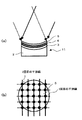
第2の実施形態の金型11で成型されたレンズの略錐形状25は、図5に示すように、その形状の先端部に平面部26が形成されている。図5は、成型されたレンズが持つ略錐形状25を模式的に示す断面図である。また、図6は作製された金型の錘形状20を模式的に示している。図6(a)は金型の錘形状の斜視図、図6(b)は錘形状の底部での横断面図である。図6(a)においては、金型のレンズ成型面の極一部を切り出して表示しているため、平面上に錘形状が形成されているように示されているが、実際は金型のレンズ形成面全面に錘形状20が形成されている。図6(b)に示すように、錘形状20の底面部には平面部21を有しているため、成型を行うと、この平面部21が略錐形状25の先端部に転写される。このように、先端部に平面部26を有し、また錘形状20と相補的な関係をなす略錐形状25は、完全な錘形状ではないが、図6(a)に示すような錘形状をレンズ面に有する場合と比較して、反射防止構造としては、実用上性能に差はない。
【0057】
なお、上記第1および第2の実施の形態では、レンズ面上に微細構造を有しているが、光学素子はレンズに限らず、例えば曲面を有するミラー面上にCGH等の微細構造を有してもよい。
【0058】
【発明の効果】
請求項1の発明では、金型母材上に加工層を形成し、その加工層にレンズ面等に対応する曲面を機械加工し、さらにその上に積層されたエッチング層に微細構造を形成している。そのため光学素子用金型の面精度は機械加工によって確保され、また微細構造の形状精度はエッチング層のエッチングによって得られる。その結果、高精度な金型が得られ、そのような金型を用いることで、高精度な光学素子を容易に低コストで大量に生産することができる。
【0059】
また、加工層に、曲面の機械加工を容易に行うことができる切削性のよい材料を使用するため、金型に剛性のある材料を用いることができる。さらに、エッチングの際に加工層が露出したとしても、エッチングされ難い材料のため、エッチングされることがなく、金型のレンズ面は良好な面精度、面粗さが得られる。また、エッチングされ難い特性を利用して、容易に微細構造の高さを制御できる。
【0060】
請求項4の発明では、加工層をレンズ面等の曲面に機械加工し、その上に形成されたエッチング層に微細構造を形成するため、機械加工による面精度の確保と複雑な微細構造とが同時に得られる光学素子用金型を製造することができる。そのような光学素子用金型を使用することで、高精度な光学素子を容易に低コストで大量に生産することができる。
【図面の簡単な説明】
【図1】第1の実施の形態の金型を模式的に示す縦断面図である。
【図2】第1の実施の形態の金型の製造工程を模式的に示す縦断面図である。
【図3】第2の実施の形態の金型の製造工程を模式的に示す縦断面図である。
【図4】錐形状を露光するための方法を説明する図である。
【図5】第2の実施の形態の金型を用いて成型されたレンズの、反射防止構造を拡大して示す縦断面図である。
【図6】第2の実施の形態の金型の錘形状を拡大して示す図である。
【図7】CGHレンズの例を模式的に示す図である。
【図8】CGHを模式的に示す縦断面図である。
【符号の説明】
1、11 金型
2 金型母材
3 加工層
4 エッチング層
5 レジスト
6 クロム膜(金属マスク)
15 CGHレンズ
16 CGH
17 光源
20 錐形状
21 平面部(錐形状底面)
25 略錐形状
26 平面部(略錐形状先端)[0001]
TECHNICAL FIELD OF THE INVENTION
The present invention relates to a mold for an optical element, and more particularly to a mold for molding an optical element having a fine structure on a curved surface. The invention also relates to a method for manufacturing such a mold.
[0002]
[Prior art]
[Patent Document 1]
JP-A-62-96902 [Patent Document 2]
Japanese Patent Application Laid-Open No. 2000-182024 [Patent Document 3]
JP 2002-326231 A [Patent Document 4]
JP-A-2002-274865
In recent years, it has been required to form a diffraction grating having a complicated structure typified by CGH (Computer Generated Hologram) or a fine structure for preventing reflection without using a deposited film on an optical element such as a lens surface. ing. For example, by integrating the CGH with the lens, one lens can realize the light-collecting (image-forming) function of the lens and another function by diffraction. Further, if a fine structure for performing anti-reflection is formed on the lens surface, higher-performance anti-reflection can be performed. That is, by forming these microstructures on the lens surface, it is possible to make the optical system highly functional, compact, and high-performance.
[0004]
On the other hand, in order to mass produce such an optical element at low cost, a mold is manufactured, and the mold shape is transferred to a synthetic resin material. In this case, it is necessary to process the shape of the lens surface and the fine structure in the mold. Molds having such a shape are described in
[0005]
The mold described in
[0006]
The mold described in
[0007]
On the other hand, there is also widely used a method in which a required element shape is manufactured as a master mold, and the shape of the master mold is copied by electroforming to form a mold.
[0008]
[Problems to be solved by the invention]
However, since the mold described in
[0009]
The mold described in
[0010]
The method of making a mold by electroforming makes it easy to duplicate the mold as long as a master mold is made. However, when high-performance imaging (light collecting) characteristics are required, it is not suitable for the following reasons. It is. In electroforming, as the thickness of the electroformed layer increases, a very large stress is generated inside. Therefore, the moment the electroformed layer is separated from the master mold, the mold surface is distorted. In a high-performance lens, since the surface accuracy of the lens surface is required to be equal to or less than the wavelength, an electroformed mold having a large distortion is not suitable for a high-performance lens.
[0011]
The present invention has been made in view of such a situation, and is an optical element for duplicating an optical element that achieves both high-performance optical action due to the curved surface of the optical element and optical action due to the fine structure. It is an object to provide a mold. Another object is to provide a method for manufacturing such a mold.
[0012]
[Means for Solving the Problems]
In order to achieve the above object, an invention according to
[0013]
According to a second aspect of the present invention, in the mold for an optical element according to the first aspect, the processed layer is made of any one of nickel, a nickel alloy, copper, a copper alloy, and brass.
[0014]
The invention according to
[0015]
The invention according to
[0016]
BEST MODE FOR CARRYING OUT THE INVENTION
Hereinafter, embodiments of the present invention will be described with reference to the drawings. The mold according to the first embodiment is a mold for molding a lens in which a lens surface and CGH are integrally formed. The CGH is a hologram created by calculating the distribution of the amplitude and phase of light to be recorded based on diffraction by a virtual object, and drawing the distribution. As shown in FIG. 8, the CGH of the present embodiment includes a large number of rectangular diffraction gratings formed at various intervals on a lens surface. In FIG. 8, the diffraction grating is described only one-dimensionally, but the direction of the periodic arrangement of the diffraction grating is two-dimensionally arranged in various directions. Hereinafter, the diffraction grating is referred to as CGH, and the lens having the CGH formed on the lens surface is referred to as a CGH lens.
[0017]
First, the
[0018]
Next, a method of manufacturing the
[0019]
(A) The
[0020]
(B) A nickel material is laminated to a thickness of 5 mm by electroforming on the
[0021]
(C) A desired optical mirror surface corresponding to the lens surface is formed on the
[0022]
As the mold base material, a material having high rigidity such as stainless steel is preferable, but it is difficult to form an optical mirror surface on an iron-based material such as stainless steel. It is for the following reasons. Generally, a diamond tool is used in mirror finishing, but if a diamond tool is used for iron-based material, an oxidation reaction occurs, and the diamond tool burns or excessively wears. . In this embodiment, an optical mirror surface is obtained by laminating a material having excellent machinability as a processing layer on a mold base material and processing the processing layer with high accuracy.
[0023]
(D) On the processed surface of the processed
The conditions for forming the TiN film are as follows.
Set temperature: 300 ° C., pressure: 1.3 Pa, gas: Ar (argon),
Gas flow rate: 10 sccm, applied power: 500 W
It is.
[0024]
The material of the film is not limited to TiN, but Si (silicon), SiO 2 (silicon dioxide), Al (aluminum), SiN (silicon nitride), Mo (molybdenum), SiC (silicon carbide), WC (tungsten carbide) ). The
[0025]
(E) A resist 5 is applied on the
[0026]
(F) Exposing the diffraction grating pattern corresponding to CGH. In this embodiment, since exposure is performed on a curved surface, it is difficult to perform exposure using a conventional exposure apparatus. However, exposure is performed by a method using an electron beam lithography apparatus described later.
[0027]
(G) The resist 5 is developed. The exposed portions of the resist are removed by development, and the processed
[0028]
(H) The etching layer 4 (TiN) is etched by a dry etching method to form
[0029]
[Table 1]
In Table 1, RF is high frequency applied power of 13.56 MHz. In addition, when two types of gas are described in the gas type column with / (slash) therebetween, it means a mixed gas thereof. In the flow rate column, values described between / (slash) are the flow rates for each gas type described in the gas type column.
[0031]
The height of the
(1) The height of the
(2) The
[0032]
In the present embodiment, etching is performed by the above method (2) until the
(I) Unnecessary resist 5 and polymer deteriorated by dry etching are removed by ashing (ashing).
[0033]
FIG. 1A is a longitudinal sectional view schematically showing the
[0034]
When the
[0035]
Next, a method of exposing a diffraction grating pattern on a curved surface regarding the step (F) will be described. In the present embodiment, the
[0036]
(Exposure method 1) This is a method using an electron beam drawing apparatus. Since an electron beam lithography apparatus generally performs exposure on a flat surface, when exposing on a curved surface, a desired fine shape cannot be drawn because the focal position does not match the drawing surface. Therefore, exposure is performed while moving the object to be exposed or the drawing apparatus (optical system) in the optical axis direction so as to compensate for the curved surface shape. This method is effective not only for electron beams but also for laser exposure apparatuses.
[0037]
(Exposure method 2) A contact exposure method. This is effective when the shape of the workpiece is large and the grating period of the diffraction grating pattern is large. However, when the curvature of the lens surface is large and the deviation from the plane is large, the lattice pattern is blurred. If the grating period is about 50 microns, it is possible to expose even a plane about 2 mm away from a plane. When the lattice period is large and the area of the workpiece (mold) is large, it is easier to fabricate using the contact exposure method.
[0038]
(Exposure method 3) This is a method using a projection exposure apparatus. The optical system of the projection exposure apparatus has image surface characteristics and distortion characteristics corresponding to the lens surface shape of the mold.
[0039]
The exposure of the diffraction grating pattern on the curved surface can be performed by using any of the above three exposure methods.
[0040]
Next, a lens mold having an antireflection fine structure according to a second embodiment will be described. It is known that an antireflection effect can be obtained with respect to light having a wide wavelength range by forming a conical shape finely and densely on the surface of glass or plastics. The mold of the present embodiment is for duplicating a lens having a fine shape (hereinafter, referred to as a substantially conical shape) having an action equivalent to such a conical shape as an antireflection structure.
[0041]
The lens replicated by the mold of the present embodiment is a lens of a micro lens system mounted on a mobile phone or the like, which is arranged at a position closest to the image sensor. The lens is a biconvex lens having an effective diameter of 5 mm and a radius of curvature of about 5 mm and about 250 mm. When surface reflection occurs on a surface having a large radius of curvature, reflected light is incident on the image sensor and ghost occurs. When the lens is molded of a synthetic resin material, it is difficult to perform a high-performance antireflection coating with a general dielectric film, and the manufacturing cost increases. By molding the substantially cone-shaped antireflection structure at the same time as molding the lens, the manufacturing cost can be significantly reduced.
[0042]
FIG. 3 is a diagram schematically illustrating a manufacturing process of the mold according to the second embodiment. Hereinafter, the method of manufacturing the mold will be described with reference to FIG.
[0043]
(A) A
[0044]
(B) A nickel material is laminated to a thickness of 5 mm by electroforming on the
[0045]
(C) A desired optical mirror surface corresponding to the lens surface is formed on the
[0046]
(D) A TiN (titanium nitride) film is formed on the processed surface of the processed
[0047]
The material of the film is not limited to TiN, but Si (silicon), SiO 2 (silicon dioxide), Al (aluminum), SiN (silicon nitride), Mo (molybdenum), SiC (silicon carbide), WC (tungsten carbide) ). The
[0048]
(E) A resist 5 is applied on the
[0049]
(F) Exposure of a pattern for forming a conical shape. FIG. 4 shows an exposure method. The laser beam is separated into two light beams (not shown), and the separated two light beams are incident on the resist 5 at an angle to each other as shown in FIG. Interference fringes are generated on the resist 5, and the interference fringe shape is exposed. When the
[0050]
(G) The resist 5 is developed. The black circle shown in FIG. 4B has a larger exposure amount than the other regions, so that a hole reaching the
[0051]
(H) A chromium film 6 is formed on the developed resist 5 by a vacuum evaporation method. The chromium film 6 is deposited on both the surface of the resist 5 and the
[0052]
(I) The resist 5 is removed, and the chromium film 6 (hereinafter, referred to as a metal mask) formed on the four etching layers is exposed on the surface (lift-off).
[0053]
(J) Perform dry etching on the mold. The etching conditions are the conditions shown in Table 1 described in the first embodiment. When dry etching is started, first, etching is started in a tapered shape from a position where the metal mask 6 on the etching layer is not present. Then, as the etching proceeds, the metal mask 6 is also gradually etched, and the
[0054]
(K) The unnecessary chromium film 6 remaining on the
[0055]
Using the
[0056]
As shown in FIG. 5, a substantially
[0057]
In the first and second embodiments, the fine structure is provided on the lens surface. However, the optical element is not limited to the lens. For example, the fine structure such as CGH is provided on the mirror surface having a curved surface. May be.
[0058]
【The invention's effect】
According to the first aspect of the present invention, a processed layer is formed on a mold base material, a curved surface corresponding to a lens surface or the like is machined on the processed layer, and a fine structure is formed on an etching layer laminated thereon. ing. Therefore, the surface accuracy of the optical element mold is ensured by machining, and the fine structure shape accuracy is obtained by etching the etching layer. As a result, a high-precision mold is obtained, and by using such a mold, high-precision optical elements can be easily mass-produced at low cost.
[0059]
In addition, since a material having good machinability, which can easily perform machining of a curved surface, is used for the processing layer, a rigid material can be used for the mold. Furthermore, even if the processed layer is exposed during the etching, the material is difficult to be etched, so that the material is not etched, and the lens surface of the mold can have good surface accuracy and surface roughness. In addition, the height of the fine structure can be easily controlled by using the characteristic that is hardly etched.
[0060]
According to the fourth aspect of the present invention, the processing layer is machined into a curved surface such as a lens surface, and a fine structure is formed on the etching layer formed thereon. A mold for an optical element obtained at the same time can be manufactured. By using such a mold for an optical element, a high-precision optical element can be easily mass-produced at low cost.
[Brief description of the drawings]
FIG. 1 is a longitudinal sectional view schematically showing a mold according to a first embodiment.
FIG. 2 is a longitudinal sectional view schematically showing a manufacturing process of the mold according to the first embodiment.
FIG. 3 is a longitudinal sectional view schematically showing a manufacturing process of a mold according to a second embodiment.
FIG. 4 is a diagram illustrating a method for exposing a conical shape.
FIG. 5 is an enlarged longitudinal sectional view of an anti-reflection structure of a lens molded using a mold according to a second embodiment.
FIG. 6 is an enlarged view showing a weight shape of a mold according to the second embodiment.
FIG. 7 is a diagram schematically illustrating an example of a CGH lens.
FIG. 8 is a longitudinal sectional view schematically showing a CGH.
[Explanation of symbols]
1, 11
15
17
25 Substantially
Claims (4)
金型母材上に加工層を形成する工程と、
加工層を所望の光学鏡面に加工する工程と
加工された加工層上にエッチング層を形成する工程と、
エッチング層上にレジストを塗布する工程と、
レジストに微細構造パターンを描画し現像処理により微細構造パターンを転写する工程と、
エッチング処理によってエッチング層に微細構造を形成する工程と、
を含み、曲面と微細構造を一体的に作製することを特徴とする光学素子用金型の製造方法。A method for manufacturing a mold for an optical element for molding an optical element having a fine structure on a curved surface,
Forming a working layer on the mold base material;
A step of processing the processing layer into a desired optical mirror surface and a step of forming an etching layer on the processed processing layer,
A step of applying a resist on the etching layer,
A step of drawing a fine structure pattern on a resist and transferring the fine structure pattern by a development process;
Forming a fine structure in the etching layer by an etching process;
Wherein the curved surface and the fine structure are integrally formed.
Priority Applications (1)
| Application Number | Priority Date | Filing Date | Title |
|---|---|---|---|
| JP2003060235A JP4218372B2 (en) | 2003-03-06 | 2003-03-06 | Manufacturing method of mold for optical element |
Applications Claiming Priority (1)
| Application Number | Priority Date | Filing Date | Title |
|---|---|---|---|
| JP2003060235A JP4218372B2 (en) | 2003-03-06 | 2003-03-06 | Manufacturing method of mold for optical element |
Publications (2)
| Publication Number | Publication Date |
|---|---|
| JP2004268331A true JP2004268331A (en) | 2004-09-30 |
| JP4218372B2 JP4218372B2 (en) | 2009-02-04 |
Family
ID=33122841
Family Applications (1)
| Application Number | Title | Priority Date | Filing Date |
|---|---|---|---|
| JP2003060235A Expired - Fee Related JP4218372B2 (en) | 2003-03-06 | 2003-03-06 | Manufacturing method of mold for optical element |
Country Status (1)
| Country | Link |
|---|---|
| JP (1) | JP4218372B2 (en) |
Cited By (9)
| Publication number | Priority date | Publication date | Assignee | Title |
|---|---|---|---|---|
| WO2005092588A1 (en) * | 2004-03-25 | 2005-10-06 | Sanyo Electric Co., Ltd. | Production method of curved-surface metal mold having fine uneven structure and production method of optical element using this metal mold |
| JP2006178213A (en) * | 2004-12-22 | 2006-07-06 | Sanyo Electric Co Ltd | Method for manufacturing die and optical element formed by using the die |
| JP2006243633A (en) * | 2005-03-07 | 2006-09-14 | Matsushita Electric Ind Co Ltd | Manufacturing method of member having antireflection structure body |
| WO2006126520A1 (en) * | 2005-05-24 | 2006-11-30 | Matsushita Electric Industrial Co., Ltd. | Dry etching method, method for forming fine structure, mold and method for producing same |
| JP2009155167A (en) * | 2007-12-27 | 2009-07-16 | Kanagawa Prefecture | Method for processing object to be processed, method for molding glass or resin, mold, and molded article of glass or resin |
| JP2013171253A (en) * | 2012-02-22 | 2013-09-02 | Dainippon Printing Co Ltd | Retardation film production plate and method of manufacturing retardation film production plate |
| KR20140010116A (en) * | 2011-03-16 | 2014-01-23 | 칼 짜이스 레이저 옵틱스 게엠베하 | Method for producing a reflective optical component for an euv projection exposure apparatus and component of this type |
| WO2014092132A1 (en) | 2012-12-13 | 2014-06-19 | 王子ホールディングス株式会社 | Mold for manufacturing optical element and production method for same, and optical element |
| JP2014115634A (en) * | 2012-12-06 | 2014-06-26 | Tatung Co | Antireflection substrate structure and manufacturing method thereof |
-
2003
- 2003-03-06 JP JP2003060235A patent/JP4218372B2/en not_active Expired - Fee Related
Cited By (13)
| Publication number | Priority date | Publication date | Assignee | Title |
|---|---|---|---|---|
| WO2005092588A1 (en) * | 2004-03-25 | 2005-10-06 | Sanyo Electric Co., Ltd. | Production method of curved-surface metal mold having fine uneven structure and production method of optical element using this metal mold |
| JP2006178213A (en) * | 2004-12-22 | 2006-07-06 | Sanyo Electric Co Ltd | Method for manufacturing die and optical element formed by using the die |
| JP2006243633A (en) * | 2005-03-07 | 2006-09-14 | Matsushita Electric Ind Co Ltd | Manufacturing method of member having antireflection structure body |
| WO2006126520A1 (en) * | 2005-05-24 | 2006-11-30 | Matsushita Electric Industrial Co., Ltd. | Dry etching method, method for forming fine structure, mold and method for producing same |
| US7919005B2 (en) | 2005-05-24 | 2011-04-05 | Panasonic Corporation | Dry etching method, fine structure formation method, mold and mold fabrication method |
| JP2009155167A (en) * | 2007-12-27 | 2009-07-16 | Kanagawa Prefecture | Method for processing object to be processed, method for molding glass or resin, mold, and molded article of glass or resin |
| KR102085237B1 (en) * | 2011-03-16 | 2020-03-05 | 칼 짜이스 에스엠티 게엠베하 | Method for producing a reflective optical component for an euv projection exposure apparatus and component of this type |
| KR20140010116A (en) * | 2011-03-16 | 2014-01-23 | 칼 짜이스 레이저 옵틱스 게엠베하 | Method for producing a reflective optical component for an euv projection exposure apparatus and component of this type |
| JP2013171253A (en) * | 2012-02-22 | 2013-09-02 | Dainippon Printing Co Ltd | Retardation film production plate and method of manufacturing retardation film production plate |
| JP2014115634A (en) * | 2012-12-06 | 2014-06-26 | Tatung Co | Antireflection substrate structure and manufacturing method thereof |
| US9224893B2 (en) | 2012-12-06 | 2015-12-29 | Tatung Company | Antireflection substrate structure and manufacturing method thereof |
| US9915758B2 (en) | 2012-12-13 | 2018-03-13 | Oji Holdings Corporation | Mold for manufacturing optical element and production method for same, and optical element |
| WO2014092132A1 (en) | 2012-12-13 | 2014-06-19 | 王子ホールディングス株式会社 | Mold for manufacturing optical element and production method for same, and optical element |
Also Published As
| Publication number | Publication date |
|---|---|
| JP4218372B2 (en) | 2009-02-04 |
Similar Documents
| Publication | Publication Date | Title |
|---|---|---|
| US7455957B2 (en) | Blazed holographic grating, method for producing the same and replica grating | |
| US7129028B2 (en) | Method of forming holographic grating | |
| US7760435B2 (en) | Method of fabricating tridimensional micro- and nanostructures as well as optical element assembly having a tridimensional convex structure obtained by the method | |
| JP2004012856A (en) | Optical element, mold for optical element, and method for manufacturing optical element | |
| JP2004268331A (en) | Mold for molding optical element and method for manufacturing mold | |
| JP3877444B2 (en) | Diffraction grating | |
| JP5852123B2 (en) | High contrast alignment mark by multi-stage imprint | |
| JP2005132660A (en) | Manufacturing method of optical element having non-reflective structure and optical element having non-reflective structure manufactured through the method | |
| JP2006317807A (en) | Member equipped with antireflection structure and manufacturing method of the member | |
| JPH1172606A (en) | Pattern etching method for sic | |
| JP2006243633A (en) | Manufacturing method of member having antireflection structure body | |
| JPH11160510A (en) | Manufacture of multistage staircase-like element and manufacture of mold for manufacturing the element | |
| JP5066815B2 (en) | Reflective diffraction grating | |
| JPH10337734A (en) | Mold and its manufacture | |
| JP2001296416A (en) | Method for manufacturing device or method for manufacturing diffraction optical device, and die for manufacture of diffraction optical device, diffraction optical device and optical system such as optical appliance by that method for manufacturing diffraction optical device | |
| JPH0322601B2 (en) | ||
| WO2020031945A1 (en) | Optical element with anti-reflection structure, method for producing same, method for producing production mold, and imaging device | |
| JP4594745B2 (en) | Method for manufacturing member having antireflection structure | |
| JP5671843B2 (en) | Tray for dry etching, dry etching method using the same, method for producing tray, and method for producing mold | |
| JPH0226851B2 (en) | ||
| JPH0915410A (en) | Production of optical element and production of metal mold for optical element | |
| JPH08227007A (en) | Formation of surface shape of object and production of metal mold | |
| JPS6249094B2 (en) | ||
| JP4534709B2 (en) | Diamond parts manufacturing method | |
| JP4262514B2 (en) | Manufacturing method of optical member |
Legal Events
| Date | Code | Title | Description |
|---|---|---|---|
| A711 | Notification of change in applicant |
Free format text: JAPANESE INTERMEDIATE CODE: A712 Effective date: 20050325 |
|
| A621 | Written request for application examination |
Effective date: 20050330 Free format text: JAPANESE INTERMEDIATE CODE: A621 |
|
| A977 | Report on retrieval |
Effective date: 20061003 Free format text: JAPANESE INTERMEDIATE CODE: A971007 |
|
| A131 | Notification of reasons for refusal |
Free format text: JAPANESE INTERMEDIATE CODE: A131 Effective date: 20070626 |
|
| A521 | Written amendment |
Free format text: JAPANESE INTERMEDIATE CODE: A523 Effective date: 20070822 |
|
| TRDD | Decision of grant or rejection written | ||
| A01 | Written decision to grant a patent or to grant a registration (utility model) |
Free format text: JAPANESE INTERMEDIATE CODE: A01 Effective date: 20081021 |
|
| A01 | Written decision to grant a patent or to grant a registration (utility model) |
Free format text: JAPANESE INTERMEDIATE CODE: A01 |
|
| A61 | First payment of annual fees (during grant procedure) |
Free format text: JAPANESE INTERMEDIATE CODE: A61 Effective date: 20081103 |
|
| FPAY | Renewal fee payment (prs date is renewal date of database) |
Free format text: PAYMENT UNTIL: 20111121 Year of fee payment: 3 |
|
| R150 | Certificate of patent (=grant) or registration of utility model |
Free format text: JAPANESE INTERMEDIATE CODE: R150 |
|
| FPAY | Renewal fee payment (prs date is renewal date of database) |
Year of fee payment: 3 Free format text: PAYMENT UNTIL: 20111121 |
|
| FPAY | Renewal fee payment (prs date is renewal date of database) |
Year of fee payment: 4 Free format text: PAYMENT UNTIL: 20121121 |
|
| LAPS | Cancellation because of no payment of annual fees |