WO2011102100A1 - Semiconductor device and stacked-type semiconductor device - Google Patents
Semiconductor device and stacked-type semiconductor device Download PDFInfo
- Publication number
- WO2011102100A1 WO2011102100A1 PCT/JP2011/000742 JP2011000742W WO2011102100A1 WO 2011102100 A1 WO2011102100 A1 WO 2011102100A1 JP 2011000742 W JP2011000742 W JP 2011000742W WO 2011102100 A1 WO2011102100 A1 WO 2011102100A1
- Authority
- WO
- WIPO (PCT)
- Prior art keywords
- solder
- electrodes
- interposer substrate
- openings
- semiconductor device
- Prior art date
- Legal status (The legal status is an assumption and is not a legal conclusion. Google has not performed a legal analysis and makes no representation as to the accuracy of the status listed.)
- Ceased
Links
Images







Classifications
-
- H—ELECTRICITY
- H10—SEMICONDUCTOR DEVICES; ELECTRIC SOLID-STATE DEVICES NOT OTHERWISE PROVIDED FOR
- H10W—GENERIC PACKAGES, INTERCONNECTIONS, CONNECTORS OR OTHER CONSTRUCTIONAL DETAILS OF DEVICES COVERED BY CLASS H10
- H10W90/00—Package configurations
-
- H—ELECTRICITY
- H10—SEMICONDUCTOR DEVICES; ELECTRIC SOLID-STATE DEVICES NOT OTHERWISE PROVIDED FOR
- H10W—GENERIC PACKAGES, INTERCONNECTIONS, CONNECTORS OR OTHER CONSTRUCTIONAL DETAILS OF DEVICES COVERED BY CLASS H10
- H10W42/00—Arrangements for protection of devices
- H10W42/121—Arrangements for protection of devices protecting against mechanical damage
-
- H—ELECTRICITY
- H10—SEMICONDUCTOR DEVICES; ELECTRIC SOLID-STATE DEVICES NOT OTHERWISE PROVIDED FOR
- H10W—GENERIC PACKAGES, INTERCONNECTIONS, CONNECTORS OR OTHER CONSTRUCTIONAL DETAILS OF DEVICES COVERED BY CLASS H10
- H10W70/00—Package substrates; Interposers; Redistribution layers [RDL]
- H10W70/60—Insulating or insulated package substrates; Interposers; Redistribution layers
- H10W70/67—Insulating or insulated package substrates; Interposers; Redistribution layers characterised by their insulating layers or insulating parts
- H10W70/68—Shapes or dispositions thereof
- H10W70/685—Shapes or dispositions thereof comprising multiple insulating layers
- H10W70/687—Shapes or dispositions thereof comprising multiple insulating layers characterized by the outer layers being for protection, e.g. solder masks, or for protection against chemical or mechanical damage
-
- H—ELECTRICITY
- H10—SEMICONDUCTOR DEVICES; ELECTRIC SOLID-STATE DEVICES NOT OTHERWISE PROVIDED FOR
- H10W—GENERIC PACKAGES, INTERCONNECTIONS, CONNECTORS OR OTHER CONSTRUCTIONAL DETAILS OF DEVICES COVERED BY CLASS H10
- H10W90/00—Package configurations
- H10W90/701—Package configurations characterised by the relative positions of pads or connectors relative to package parts
-
- H—ELECTRICITY
- H10—SEMICONDUCTOR DEVICES; ELECTRIC SOLID-STATE DEVICES NOT OTHERWISE PROVIDED FOR
- H10W—GENERIC PACKAGES, INTERCONNECTIONS, CONNECTORS OR OTHER CONSTRUCTIONAL DETAILS OF DEVICES COVERED BY CLASS H10
- H10W99/00—Subject matter not provided for in other groups of this subclass
-
- H—ELECTRICITY
- H05—ELECTRIC TECHNIQUES NOT OTHERWISE PROVIDED FOR
- H05K—PRINTED CIRCUITS; CASINGS OR CONSTRUCTIONAL DETAILS OF ELECTRIC APPARATUS; MANUFACTURE OF ASSEMBLAGES OF ELECTRICAL COMPONENTS
- H05K1/00—Printed circuits
- H05K1/02—Details
- H05K1/14—Structural association of two or more printed circuits
- H05K1/144—Stacked arrangements of planar printed circuit boards
-
- H—ELECTRICITY
- H10—SEMICONDUCTOR DEVICES; ELECTRIC SOLID-STATE DEVICES NOT OTHERWISE PROVIDED FOR
- H10W—GENERIC PACKAGES, INTERCONNECTIONS, CONNECTORS OR OTHER CONSTRUCTIONAL DETAILS OF DEVICES COVERED BY CLASS H10
- H10W70/00—Package substrates; Interposers; Redistribution layers [RDL]
- H10W70/60—Insulating or insulated package substrates; Interposers; Redistribution layers
- H10W70/67—Insulating or insulated package substrates; Interposers; Redistribution layers characterised by their insulating layers or insulating parts
- H10W70/68—Shapes or dispositions thereof
-
- H—ELECTRICITY
- H10—SEMICONDUCTOR DEVICES; ELECTRIC SOLID-STATE DEVICES NOT OTHERWISE PROVIDED FOR
- H10W—GENERIC PACKAGES, INTERCONNECTIONS, CONNECTORS OR OTHER CONSTRUCTIONAL DETAILS OF DEVICES COVERED BY CLASS H10
- H10W70/00—Package substrates; Interposers; Redistribution layers [RDL]
- H10W70/60—Insulating or insulated package substrates; Interposers; Redistribution layers
- H10W70/67—Insulating or insulated package substrates; Interposers; Redistribution layers characterised by their insulating layers or insulating parts
- H10W70/68—Shapes or dispositions thereof
- H10W70/685—Shapes or dispositions thereof comprising multiple insulating layers
-
- H—ELECTRICITY
- H10—SEMICONDUCTOR DEVICES; ELECTRIC SOLID-STATE DEVICES NOT OTHERWISE PROVIDED FOR
- H10W—GENERIC PACKAGES, INTERCONNECTIONS, CONNECTORS OR OTHER CONSTRUCTIONAL DETAILS OF DEVICES COVERED BY CLASS H10
- H10W72/00—Interconnections or connectors in packages
- H10W72/851—Dispositions of multiple connectors or interconnections
- H10W72/874—On different surfaces
- H10W72/884—Die-attach connectors and bond wires
-
- H—ELECTRICITY
- H10—SEMICONDUCTOR DEVICES; ELECTRIC SOLID-STATE DEVICES NOT OTHERWISE PROVIDED FOR
- H10W—GENERIC PACKAGES, INTERCONNECTIONS, CONNECTORS OR OTHER CONSTRUCTIONAL DETAILS OF DEVICES COVERED BY CLASS H10
- H10W74/00—Encapsulations, e.g. protective coatings
-
- H—ELECTRICITY
- H10—SEMICONDUCTOR DEVICES; ELECTRIC SOLID-STATE DEVICES NOT OTHERWISE PROVIDED FOR
- H10W—GENERIC PACKAGES, INTERCONNECTIONS, CONNECTORS OR OTHER CONSTRUCTIONAL DETAILS OF DEVICES COVERED BY CLASS H10
- H10W74/00—Encapsulations, e.g. protective coatings
- H10W74/10—Encapsulations, e.g. protective coatings characterised by their shape or disposition
- H10W74/111—Encapsulations, e.g. protective coatings characterised by their shape or disposition the semiconductor body being completely enclosed
- H10W74/114—Encapsulations, e.g. protective coatings characterised by their shape or disposition the semiconductor body being completely enclosed by a substrate and the encapsulations
-
- H—ELECTRICITY
- H10—SEMICONDUCTOR DEVICES; ELECTRIC SOLID-STATE DEVICES NOT OTHERWISE PROVIDED FOR
- H10W—GENERIC PACKAGES, INTERCONNECTIONS, CONNECTORS OR OTHER CONSTRUCTIONAL DETAILS OF DEVICES COVERED BY CLASS H10
- H10W90/00—Package configurations
- H10W90/701—Package configurations characterised by the relative positions of pads or connectors relative to package parts
- H10W90/721—Package configurations characterised by the relative positions of pads or connectors relative to package parts of bump connectors
- H10W90/722—Package configurations characterised by the relative positions of pads or connectors relative to package parts of bump connectors between stacked chips
-
- H—ELECTRICITY
- H10—SEMICONDUCTOR DEVICES; ELECTRIC SOLID-STATE DEVICES NOT OTHERWISE PROVIDED FOR
- H10W—GENERIC PACKAGES, INTERCONNECTIONS, CONNECTORS OR OTHER CONSTRUCTIONAL DETAILS OF DEVICES COVERED BY CLASS H10
- H10W90/00—Package configurations
- H10W90/701—Package configurations characterised by the relative positions of pads or connectors relative to package parts
- H10W90/721—Package configurations characterised by the relative positions of pads or connectors relative to package parts of bump connectors
- H10W90/724—Package configurations characterised by the relative positions of pads or connectors relative to package parts of bump connectors between a chip and a stacked insulating package substrate, interposer or RDL
-
- H—ELECTRICITY
- H10—SEMICONDUCTOR DEVICES; ELECTRIC SOLID-STATE DEVICES NOT OTHERWISE PROVIDED FOR
- H10W—GENERIC PACKAGES, INTERCONNECTIONS, CONNECTORS OR OTHER CONSTRUCTIONAL DETAILS OF DEVICES COVERED BY CLASS H10
- H10W90/00—Package configurations
- H10W90/701—Package configurations characterised by the relative positions of pads or connectors relative to package parts
- H10W90/731—Package configurations characterised by the relative positions of pads or connectors relative to package parts of die-attach connectors
- H10W90/734—Package configurations characterised by the relative positions of pads or connectors relative to package parts of die-attach connectors between a chip and a stacked insulating package substrate, interposer or RDL
-
- H—ELECTRICITY
- H10—SEMICONDUCTOR DEVICES; ELECTRIC SOLID-STATE DEVICES NOT OTHERWISE PROVIDED FOR
- H10W—GENERIC PACKAGES, INTERCONNECTIONS, CONNECTORS OR OTHER CONSTRUCTIONAL DETAILS OF DEVICES COVERED BY CLASS H10
- H10W90/00—Package configurations
- H10W90/701—Package configurations characterised by the relative positions of pads or connectors relative to package parts
- H10W90/751—Package configurations characterised by the relative positions of pads or connectors relative to package parts of bond wires
- H10W90/754—Package configurations characterised by the relative positions of pads or connectors relative to package parts of bond wires between a chip and a stacked insulating package substrate, interposer or RDL
Definitions
- the present invention relates to semiconductor devices and stacked-type semiconductor devices in which solder bumps serve as external connection terminals.
- CSPs chip scale packages
- BGA ball grid array
- Warping of the CSP or the BGA package causes a gap to form between terminal electrodes of the semiconductor device and board electrodes of the printed wiring board when the semiconductor device and the printed wiring board are joined to each other, causing defective solder joints to occur.
- the connection terminals of the CSP or the BGA package are to be arranged at a narrow pitch, it is necessary to reduce the volume of the solder bumps to prevent the occurrence of bridging between the solder bumps. This results in reduced height of the solder bumps.
- PTL 1 discusses a method that reduces the occurrence of defective joints by gradually increasing the height of the solder bumps relative to the electrodes toward the periphery of the semiconductor device where the semiconductor device is warped by a great amount.
- PTL 1 proposes two methods, namely, a method in which the supply of solder bumps is uniform but the diameter of openings in a resist is reduced toward the periphery of an interposer substrate, and a method in which the supply of solder bumps is gradually increased toward the periphery of the interposer substrate.
- the reduced diameter results in a reduced joint area between the solder bumps and the electrodes. This results in increased load due to a heating cycle occurring when the power of the semiconductor device is turned on and off.
- the diameter of the openings in the resist is reduced, since the solder bumps formed on the electrodes of the interposer substrate are each formed by surface tension into a spherical shape that is larger in size than the diameter of the corresponding opening in the resist, it is difficult to ensure sufficient height for the solder bumps, resulting in a low effect for reducing the occurrence of defective solder joints between the solder bumps and the board electrodes.
- this method because the solder joint area is small in sections where the warping amount of the interposer substrate is large, the solder joint strength is reduced, and the lifespan of the solder joints is shortened.
- the lifespan of the solder joints of the solder bumps is evaluated on the basis of an accumulation of distortion occurring in the solder bumps due to a mismatch between linear coefficients of expansion of the semiconductor device and the printed wiring board. Therefore, since distortion tends to occur when the contact area of the solder joints is small, it is necessary to ensure sufficient height for the solder bumps by forming the solder bumps with a maximum possible contact area in order to extend the lifespan of the solder joints. Specifically, it is necessary to ensure flatness of the solder bumps by increasing the height of the solder bumps from the electrodes so as to compensate for the warping of the interposer substrate, so that the solder bumps can be reliably soldered to the printed wiring board.
- the present invention provides a semiconductor device that avoids the occurrence of defective solder joints caused by a reduction in size and thickness of an interposer substrate and that allows for a longer lifespan of solder joints.
- a semiconductor device mounted on a printed wiring board includes an interposer substrate having a plurality of electrodes; a semiconductor element mounted on the interposer substrate; a solder resist provided on the interposer substrate and having a plurality of openings that expose the electrodes; and a plurality of solder bumps that protrude from the openings and connect the electrodes with board electrodes of the printed wiring board.
- the solder resist that forms the openings has a height that is set to increase with increasing gap distance between the electrodes of the interposer substrate and the board electrodes of the printed wiring board.
- Figs. 1A-1B are cross-sectional views illustrating a schematic configuration of a semiconductor device according to a first embodiment of the present invention.
- Figs. 2A-2G illustrate steps for forming a solder resist.
- Fig. 3 is a cross-sectional view illustrating a schematic configuration of a semiconductor device according to a second embodiment of the present invention.
- Fig. 4 is a cross-sectional view illustrating a schematic configuration of a stacked-type semiconductor device according to another embodiment of the present invention.
- Figs. 1A and 1B illustrate a schematic configuration of a semiconductor device according to a first embodiment of the present invention.
- a semiconductor device 1 includes a semiconductor element 2 and an interposer substrate 6 with the semiconductor element 2 mounted thereon, and is mounted on a printed wiring board 11, such as a motherboard, serving as a printed wiring board.
- the surface of the interposer substrate 6 on which the semiconductor element 2 is mounted will be defined as a top surface 6a.
- the top surface 6a is provided with a wire-bonding electrode 4.
- the semiconductor element 2 and the electrode 4 are connected to each other via a wire 3.
- the semiconductor element 2, the wire 3, and the electrode 4 are covered with molded resin 7.
- a wire-bonding technique is used for the mounting of the semiconductor element 2 in the first embodiment, a flip-chip technique may be used as an alternative.
- multiple semiconductor elements may be mounted on the top surface 6a of the interposer substrate 6.
- An undersurface 6b of the interposer substrate 6 is provided with a plurality of electrodes 5a, 5b, 5c, 5d, 5e, and 5f.
- the electrodes 5b and 5e are respectively disposed at the outer side of the electrodes 5c and 5d
- the electrodes 5a and 5f are respectively disposed at the outer side of the electrodes 5b and 5e.
- the electrodes 5a to 5f are flat electrode pads and are formed in, but not limited to, for example, a circular shape in plan view.
- the semiconductor device 1 includes a solder resist 8 formed at the undersurface 6b of the interposer substrate 6.
- the solder resist 8 has a plurality of openings 8a, 8b, 8c, 8d, 8e, and 8f that are located at positions corresponding to the electrodes 5a to 5f, respectively, so as to expose the electrodes 5a to 5f.
- the openings 8b and 8e are respectively formed at the outer side of the openings 8c and 8d
- the openings 8a and 8f are respectively formed at the outer side of the openings 8b and 8e.
- the openings 8a to 8f are set to have the same diameter.
- the openings 8a to 8f are formed in, but not limited to, for example, a circular shape in plan view.
- the printed wiring board 11 is provided with the same number of board electrodes 10a, 10b, 10c, 10d, 10e, and 10f as the electrodes 5a to 5f at positions corresponding to the electrodes 5a to 5f, respectively.
- the board electrodes 10a to 10f are flat electrode pads and are formed in, but not limited to, a circular shape in plan view.
- the semiconductor device 1 includes a plurality of solder bumps 9a, 9b, 9c, 9d, 9e, and 9f that are respectively provided on the electrodes 5a to 5f.
- the solder bumps 9a to 9f are set to contain the same amount of solder. This condition in which the solder bumps 9a to 9f contain the same amount of solder includes a case where the amount of solder is within a tolerance range.
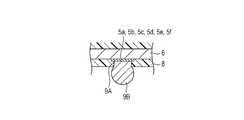
- the solder bumps 9a to 9f each have a columnar portion 9A retained by a sidewall of the corresponding opening 8a to 8f, and a solder ball portion 9B protruding from the corresponding opening 8a to 8f and not retained by the solder resist 8.
- the columnar portions 9A are connected to the corresponding electrodes 5a to 5f, and the solder ball portions 9B are connected to the corresponding board electrodes 10a to 10f.
- the solder resist 8 is composed of a solder material with low wettability so that the solder ball portions 9B of the solder bumps 9a to 9f form a protruding spherical shape without spreading over the solder resist 8.
- the interposer substrate 6 of the semiconductor device 1 can sometimes warp downward into a convex shape, as shown in Fig. 1A.
- the warping direction and the warping amount of the interposer substrate 6 are known from a preliminary experiment.
- the interposer substrate 6 is warped such that the gap distance between the electrodes 5a to 5f of the interposer substrate 6 and the board electrodes 10a to 10f of the printed wiring board 11 gradually increases from the center of the interposer substrate 6 toward the periphery thereof.
- the thickness of the solder resist 8 is set such that the height of the openings 8a to 8f from the respective electrodes 5a to 5f increases with increasing gap distance between the electrodes 5a to 5f of the interposer substrate 6 and the board electrodes 10a to 10f of the printed wiring board 11.
- the thickness of the solder resist 8 is set to increase with increasing distance from the center of the interposer substrate 6 toward the periphery thereof so as to increase the height of the openings 8a to 8f.
- the thickness of the solder resist 8 is set so as satisfy the following conditions: hc ⁇ hb ⁇ ha and hd ⁇ he ⁇ hf.
- the diameter of the solder ball portions 9B decreases with increasing height of the openings 8a to 8f. Therefore, in the first embodiment, the height of the openings 8a to 8f is adjusted, and the diameter of the solder ball portions 9B determined by the height of the openings 8a to 8f is adjusted, whereby the ends of the solder ball portions 9B of the solder bumps 9a to 9f are aligned on the same plane.
- the solder of each of the solder bumps 9a to 9f is retained by the sidewall of the corresponding opening 8a to 8f and is guided toward the corresponding board electrode 10a to 10f, thereby forming the columnar portion 9A. Consequently, the height of the solder bumps 9a to 9f can be sufficiently ensured.
- the solder ball portions 9B protruding from the openings 8a to 8f are brought close to the board electrodes 10a to 10f, and the ends of the solder ball portions 9B are aligned on the same plane.
- the solder bumps 9a to 9f are set to contain the same amount of solder. Therefore, bridging between the solder bumps 9a to 9f (for example, between the solder bump 9a and the solder bump 9b) can be avoided.
- solder ball portions 9B of the solder bumps 9a to 9f are brought close to the board electrodes 10a to 10f of the printed wiring board 11 and are aligned on the same plane so as to be connected to the board electrodes 10a to 10f. Therefore, a sufficient solder joint area can be ensured between the solder bumps 9a to 9f and the board electrodes 10a to 10f. In this case, since the openings 8a to 8f are set to have the same diameter, a sufficient joint area can be ensured between the solder bumps 9a to 9f and the electrodes 5a to 5f of the interposer substrate 6. Consequently, defective solder joints in the solder bumps 9a to 9f can be avoided, thereby extending the lifespan of solder joints.
- Techniques for forming the pattern of the solder resist 8 include a screen-printing technique using a thermosetting or ultraviolet curable ink material and a photographic technique using a photosensitive resin material. Because it is difficult to increase the positional accuracy of the solder resist 8 using the screen-printing technique, it is preferable to use the photographic technique.
- the pattern of the solder resist 8 is formed by performing a series of steps including a solder-resist application step, a pre-curing step, an exposure step, a developing step, and a main curing step.
- Figs. 2A to 2G illustrate the steps for forming the solder resist 8 by the photographic technique on the interposer substrate 6 provided with the electrodes 5a to 5f serving as a conductor pattern.
- the solder resist 8 used in the photographic technique may be formed by using either a photosensitive liquid solder resist or a dry-film solder resist. It is easier to form the solder resist 8 to an accurate height by using a dry-film solder resist having good flatness rather than using a photosensitive liquid solder resist.
- the interposer substrate 6 provided with the electrodes 5a to 5f serving as a conductor pattern is used.
- the solder resist 8 is applied onto the interposer substrate 6.
- Examples of methods for applying a liquid solder resist onto the interposer substrate 6 include a one-face application method and a double-face application method.
- the one-face application method can be performed by, for example, spraying or curtain coating, and the double-face application method can be performed by, for example, screening or roll coating.
- the first solder-resist application step is preferably performed by using a method by which the solder resist 8 can be simultaneously applied to both faces so as to prevent the conductor pattern from being contaminated.
- the applied solder resist 8 is cured in a pre-curing step. Then, an exposure step is performed by adhering a mask pattern film over the solder resist 8 and projecting light thereon. Subsequently, a developing step is performed. Consequently, as shown in Fig. 2C, openings are formed at positions corresponding to the electrodes 5a to 5f, thereby exposing the electrodes 5a to 5f. Because the exposed sections do not dissolve in a developing solution, these exposed sections remain after the developing step.
- the photosensitive solder resist may either be of a negative type in which the exposed sections do not dissolve in the developing solution, as described above, or a positive type in which the exposed sections are removed as a result of dissolving in the developing solution.
- an application step for applying the solder resist 8 to both faces of the interposer substrate 6 is performed.
- either the one-face application method or the double-face application method may be used.
- an exposure step is performed only on the face to be provided with different heights for the solder resist 8.
- a developing step is performed. Therefore, the face not to be provided with different heights for the solder resist 8 has the same height as that in Fig. 2C.
- Fig. 2F another application step for applying the solder resist 8 is performed.
- Fig. 2G an exposure step is performed by adhering a mask pattern film for only exposing sections of the solder resist 8 to be provided with different heights.
- a developing step is performed.
- the openings 8a to 8f having different heights ha to hf that gradually increase from the inner periphery toward the outer periphery of the interposer substrate 6 are formed in the solder resist 8.
- the semiconductor element 2 is mounted on the interposer substrate 6 and is sealed with resin, and the solder bumps 9a to 9f with different heights are subsequently formed.
- the openings 8c and 8d of the solder resist 8 that respectively correspond to the electrodes 5c and 5d are given a height of 20 micrometers from the electrodes 5c and 5d.
- the openings 8b and 8e of the solder resist 8 that respectively correspond to the electrodes 5b and 5e are given a height of 40 micrometers from the electrodes 5b and 5e.
- the openings 8a and 8f of the solder resist 8 that respectively correspond to the electrodes 5a and 5f are given a height of 60 micrometers from the electrodes 5a and 5f.
- the solder bumps 9a to 9f formed on the respective electrodes 5a to 5f have a diameter of 300 micrometers.
- the height from the surface of each electrode 5a to 5f to the end of the corresponding solder bump 9a to 9f is varied as follows.
- the openings 8c and 8d have a height of 20 micrometers and the solder bumps 9c and 9d have a height of 235 micrometers
- the openings 8b and 8e have a height of 40 micrometers and the solder bumps 9b and 9e have a height of 240 micrometers
- the openings 8a and 8f have a height of 60 micrometers and the solder bumps 9a and 9f have a height of 245 micrometers.
- the differences in the gap between the printed wiring board 11 and the interposer substrate 6 are complemented, and the ends of the solder bumps 9a to 9f are aligned on the same plane, thereby avoiding the occurrence of defective joints during the solder joining process.
- the heights ha, hb, and hc (hf, he, and hd) of the solder resist 8 are varied in a stepwise manner to 40 micrometers, 20 micrometers, and 20 micrometers, respectively, the occurrence of defective joints during the solder joining process can be similarly avoided.
- FIG. 3 An interposer substrate 6 of a semiconductor device 1A according to the present invention shown in Fig. 3 differs from that in the first embodiment in that the interposer substrate 6 warps upward into a convex shape during a solder joining process (210 to 240 degrees (Celsius)) of the solder bumps 9a to 9f.
- the height of the openings 8a to 8f of the solder resist 8 that respectively correspond to the electrodes 5a to 5f increases with increasing gap distance between the electrodes 5a to 5f and the board electrodes 10a to 10f.
- the height of the solder resist 8 is set such that the height of the openings 8a to 8f increases from the periphery of the interposer substrate 6 toward the center thereof.
- the thickness of the solder resist 8 is set so as satisfy the following conditions: ha ⁇ hb ⁇ hc and hf ⁇ he ⁇ hd. Consequently, the height of the openings 8a to 8f is adjusted, and the diameter of the solder ball portions 9B determined by the height of the openings 8a to 8f is adjusted, whereby the ends of the solder ball portions 9B of the solder bumps 9a to 9f are aligned on the same plane.
- the advantages similar to those in the first embodiment can be achieved. Specifically, by varying the height of the solder resist 8 from the electrodes 5a to 5f in accordance with the warping amount of the semiconductor device 1A, the differences in the gap between the printed wiring board 11 and the interposer substrate 6 are complemented, thereby avoiding the occurrence of defective joints during the solder joining process.
- the semiconductor device according to the present invention is not limited to the above-described embodiments, and design modifications are permissible so long as they are within the scope that satisfies the configuration of the invention.
- the height of the openings 8a to 8f in the solder resist 8 is gradually varied in the above-described embodiments, the height thereof may alternatively be varied in a stepwise manner.
- the printed wiring board is described as being a motherboard served by a printed wiring board in the above-described embodiments, the invention is not limited to this example. The invention is applicable to a case where the printed wiring board is served by another interposer substrate, as shown in Fig. 4.
- Fig. 4 illustrates a stacked-type semiconductor device 100 in which a first semiconductor device with a first semiconductor element mounted thereon is stacked on a second semiconductor device with a second semiconductor element mounted thereon.
- the stacked-type semiconductor device 100 has a configuration in which the semiconductor device 1 according to the first embodiment is electrically connected to an interposer substrate 26 via the solder bumps 9a to 9f.
- the interposer substrate 26 has a semiconductor element 22 mounted thereon and sends and receives a signal via at least one of the solder bumps 9a to 9f.
- a surface of the interposer substrate 26 opposite the semiconductor device 1 is provided with a plurality of solder bumps 19a to 19k that are to serve as external electrodes and to be mounted on a motherboard (not shown).
- the stacked-type semiconductor device 100 in Fig. 4 is equivalent to a configuration formed by mounting the semiconductor device 1 according to the first embodiment on the interposer substrate 26.
- this embodiment is not limited to such a configuration.
- the stacked-type semiconductor device 100 may alternatively be equivalent to a configuration formed by mounting the semiconductor device 1A according to the second embodiment on the interposer substrate 26.
- the warping shape is not limited thereto.
- the present invention is applicable to a case where the interposer substrate warps into various complex shapes.
- the interposer substrate warps into various complex shapes.
- the occurrence of defective joints can be avoided by forming the solder resist with appropriate heights in accordance the aforementioned shape.
- the height of solder bumps that are separated from the printed wiring board by a large distance can be increased by adjusting the exposed sections of the interposer substrate in accordance with the bent shape.
- the height of the openings of the solder resist is set to increase with increasing gap distance between the electrodes of the interposer substrate and the board electrodes of the printed wiring board. Therefore, sufficient height is ensured for the openings so that the solder of each of the solder bumps is retained by the corresponding opening and is guided toward the corresponding board electrode, thereby ensuring sufficient height for the solder bump. Since the solder ball portions protruding from the openings can be brought close to the board electrodes of the printed wiring board, there is no need to increase the size of the solder ball portions more than necessary by increasing the amount of solder to ensure sufficient height for the solder bumps. Therefore, bridging between the solder bumps can be avoided.
- solder ball portions are brought close to the board electrodes of the printed wiring board so as to be connected to the board electrodes of the printed wiring board, the solder joint area is increased. Consequently, defective solder joints in the solder bumps can be avoided, thereby extending the lifespan of solder joints.
Landscapes
- Electric Connection Of Electric Components To Printed Circuits (AREA)
Abstract
Description
Claims (5)
- A semiconductor device mounted on a printed wiring board, comprising:
an interposer substrate having a plurality of electrodes;
a semiconductor element mounted on the interposer substrate;
a solder resist provided on the interposer substrate and having a plurality of openings that expose the electrodes; and
a plurality of solder bumps that protrude from the openings and connect the electrodes with board electrodes of the printed wiring board,
wherein the solder resist that forms the openings has a height that is set to increase with increasing gap distance between the electrodes of the interposer substrate and the board electrodes of the printed wiring board. - The semiconductor device according to Claim 1, wherein the height of the solder resist that forms the openings gradually increases or decreases from a center of the interposer substrate toward a periphery thereof.
- The semiconductor device according to Claim 1, wherein the solder bumps each include a columnar portion that corresponds to the height of the solder resist and a solder ball portion that is not retained by the solder resist.
- The semiconductor device according to Claim 1, wherein the openings have the same diameter, and the solder bumps have the same amount of solder.
- A stacked-type semiconductor device comprising:
a first interposer substrate having a plurality of electrodes;
a first semiconductor element mounted on the first interposer substrate;
a solder resist provided on the first interposer substrate and having a plurality of openings that expose the electrodes;
a plurality of solder bumps each having a solder ball portion protruding from the corresponding opening;
a second interposer substrate connected to the solder bumps and having a plurality of electrodes;
a second semiconductor element mounted on the second interposer substrate; and
a plurality of external electrodes provided at a surface of the second interposer substrate different from a surface thereof provided with the plurality of electrodes,
wherein the solder resist that forms the openings has a height that is set to increase with increasing gap distance between the electrodes of the first interposer substrate and the electrodes of the second interposer substrate.
Priority Applications (1)
| Application Number | Priority Date | Filing Date | Title |
|---|---|---|---|
| US13/578,109 US8853866B2 (en) | 2010-02-17 | 2011-02-10 | Semiconductor device and stacked-type semiconductor device |
Applications Claiming Priority (2)
| Application Number | Priority Date | Filing Date | Title |
|---|---|---|---|
| JP2010032321A JP5409427B2 (en) | 2010-02-17 | 2010-02-17 | Printed circuit board and semiconductor device |
| JP2010-032321 | 2010-02-17 |
Publications (1)
| Publication Number | Publication Date |
|---|---|
| WO2011102100A1 true WO2011102100A1 (en) | 2011-08-25 |
Family
ID=43821858
Family Applications (1)
| Application Number | Title | Priority Date | Filing Date |
|---|---|---|---|
| PCT/JP2011/000742 Ceased WO2011102100A1 (en) | 2010-02-17 | 2011-02-10 | Semiconductor device and stacked-type semiconductor device |
Country Status (3)
| Country | Link |
|---|---|
| US (1) | US8853866B2 (en) |
| JP (1) | JP5409427B2 (en) |
| WO (1) | WO2011102100A1 (en) |
Cited By (3)
| Publication number | Priority date | Publication date | Assignee | Title |
|---|---|---|---|---|
| US9059106B2 (en) | 2012-10-31 | 2015-06-16 | International Business Machines Corporation | Compensating for warpage of a flip chip package by varying heights of a redistribution layer on an integrated circuit chip |
| TWI588958B (en) * | 2014-12-11 | 2017-06-21 | 精材科技股份有限公司 | Chip package and manufacturing method thereof |
| CN114503255A (en) * | 2019-10-04 | 2022-05-13 | 株式会社电装 | Semiconductor device with a plurality of semiconductor chips |
Families Citing this family (7)
| Publication number | Priority date | Publication date | Assignee | Title |
|---|---|---|---|---|
| US8952532B2 (en) * | 2013-05-13 | 2015-02-10 | Intel Corporation | Integrated circuit package with spatially varied solder resist opening dimension |
| KR102160786B1 (en) | 2013-10-29 | 2020-09-28 | 삼성전자주식회사 | Semiconductor Packages |
| JP6335513B2 (en) | 2014-01-10 | 2018-05-30 | 新光電気工業株式会社 | Semiconductor device and method for manufacturing semiconductor device |
| US11094658B2 (en) * | 2019-05-22 | 2021-08-17 | Lenovo (Singapore) Pte. Ltd. | Substrate, electronic substrate, and method for producing electronic substrate |
| CN112992805B (en) * | 2021-01-28 | 2022-09-27 | 日月光半导体制造股份有限公司 | Semiconductor package device and method of manufacturing the same |
| US20220359323A1 (en) * | 2021-05-07 | 2022-11-10 | Taiwan Semiconductor Manufacturing Company, Ltd. | Semiconductor package |
| TWI778835B (en) * | 2021-10-21 | 2022-09-21 | 隆達電子股份有限公司 | Electronic component sub-mount and electronic device using the same |
Citations (6)
| Publication number | Priority date | Publication date | Assignee | Title |
|---|---|---|---|---|
| US6271109B1 (en) * | 1999-07-27 | 2001-08-07 | Texas Instruments Incorporated | Substrate for accommodating warped semiconductor devices |
| JP3291368B2 (en) | 1993-07-06 | 2002-06-10 | シチズン時計株式会社 | Structure of ball grid array type semiconductor package |
| US6750549B1 (en) * | 2002-12-31 | 2004-06-15 | Intel Corporation | Variable pad diameter on the land side for improving the co-planarity of ball grid array packages |
| US20040227236A1 (en) * | 2003-03-17 | 2004-11-18 | Toshihiro Sawamoto | Semiconductor device, electronic device, electronic apparatus, and methods for manufacturing carrier substrate, semiconductor device, and electronic device |
| US6936922B1 (en) * | 2003-09-26 | 2005-08-30 | Amkor Technology, Inc. | Semiconductor package structure reducing warpage and manufacturing method thereof |
| JP2010032321A (en) | 2008-07-28 | 2010-02-12 | Yokohama National Univ | Method, device, and target member for detecting two direction movement |
Family Cites Families (5)
| Publication number | Priority date | Publication date | Assignee | Title |
|---|---|---|---|---|
| JPH08125062A (en) * | 1994-10-28 | 1996-05-17 | Seiko Epson Corp | Semiconductor device and manufacturing method thereof |
| JP3885254B2 (en) * | 1996-08-14 | 2007-02-21 | イビデン株式会社 | Method for manufacturing printed wiring board |
| JP5116268B2 (en) * | 2005-08-31 | 2013-01-09 | キヤノン株式会社 | Multilayer semiconductor device and manufacturing method thereof |
| JP4842864B2 (en) * | 2007-03-15 | 2011-12-21 | 新光電気工業株式会社 | Electronic device and manufacturing method thereof |
| KR101096039B1 (en) * | 2009-11-09 | 2011-12-19 | 주식회사 하이닉스반도체 | Printed Circuit Boards and Semiconductor Packages Using the Same |
-
2010
- 2010-02-17 JP JP2010032321A patent/JP5409427B2/en not_active Expired - Fee Related
-
2011
- 2011-02-10 US US13/578,109 patent/US8853866B2/en not_active Expired - Fee Related
- 2011-02-10 WO PCT/JP2011/000742 patent/WO2011102100A1/en not_active Ceased
Patent Citations (6)
| Publication number | Priority date | Publication date | Assignee | Title |
|---|---|---|---|---|
| JP3291368B2 (en) | 1993-07-06 | 2002-06-10 | シチズン時計株式会社 | Structure of ball grid array type semiconductor package |
| US6271109B1 (en) * | 1999-07-27 | 2001-08-07 | Texas Instruments Incorporated | Substrate for accommodating warped semiconductor devices |
| US6750549B1 (en) * | 2002-12-31 | 2004-06-15 | Intel Corporation | Variable pad diameter on the land side for improving the co-planarity of ball grid array packages |
| US20040227236A1 (en) * | 2003-03-17 | 2004-11-18 | Toshihiro Sawamoto | Semiconductor device, electronic device, electronic apparatus, and methods for manufacturing carrier substrate, semiconductor device, and electronic device |
| US6936922B1 (en) * | 2003-09-26 | 2005-08-30 | Amkor Technology, Inc. | Semiconductor package structure reducing warpage and manufacturing method thereof |
| JP2010032321A (en) | 2008-07-28 | 2010-02-12 | Yokohama National Univ | Method, device, and target member for detecting two direction movement |
Cited By (4)
| Publication number | Priority date | Publication date | Assignee | Title |
|---|---|---|---|---|
| US9059106B2 (en) | 2012-10-31 | 2015-06-16 | International Business Machines Corporation | Compensating for warpage of a flip chip package by varying heights of a redistribution layer on an integrated circuit chip |
| US9165850B2 (en) | 2012-10-31 | 2015-10-20 | Globalfoundries Inc. | Compensating for warpage of a flip chip package by varying heights of a redistribution layer on an integrated circuit chip |
| TWI588958B (en) * | 2014-12-11 | 2017-06-21 | 精材科技股份有限公司 | Chip package and manufacturing method thereof |
| CN114503255A (en) * | 2019-10-04 | 2022-05-13 | 株式会社电装 | Semiconductor device with a plurality of semiconductor chips |
Also Published As
| Publication number | Publication date |
|---|---|
| JP2011171428A (en) | 2011-09-01 |
| US20120299183A1 (en) | 2012-11-29 |
| JP5409427B2 (en) | 2014-02-05 |
| US8853866B2 (en) | 2014-10-07 |
Similar Documents
| Publication | Publication Date | Title |
|---|---|---|
| US8853866B2 (en) | Semiconductor device and stacked-type semiconductor device | |
| US8039761B2 (en) | Printed circuit board with solder bump on solder pad and flow preventing dam | |
| TWI383476B (en) | A packaged camera module with improved reliability of solder joint connections without an underfill encapsulant and method of the same | |
| JP4962217B2 (en) | Printed wiring board and electronic device manufacturing method | |
| US20100319974A1 (en) | Printed wiring board, electronic device, and method for manufacturing electronic device | |
| CN110729266B (en) | Bonding structure of package body and manufacturing method thereof | |
| US20050287705A1 (en) | Flip chip on leadframe package and method for manufacturing the same | |
| US9171814B2 (en) | Method of manufacturing semiconductor device and semiconductor device | |
| KR102511832B1 (en) | Semiconductor package device | |
| US6946601B1 (en) | Electronic package with passive components | |
| KR101565690B1 (en) | Circuit board, method for menufacturing of circuit board, electronic component package and method for menufacturing of electronic component package | |
| US20120313262A1 (en) | Stacked semiconductor device | |
| KR20090078543A (en) | Printed Circuit Boards and Semiconductor Packages Using the Same | |
| JP2014045190A (en) | Method for manufacturing printed-circuit board | |
| US10201086B2 (en) | Electronic device | |
| KR101069980B1 (en) | Method for forming solder bump | |
| US20160254241A1 (en) | Printed circuit board and soldering method | |
| KR20110013902A (en) | Package and manufacturing method | |
| KR101340348B1 (en) | Embedded chip package board using mask pattern and method for manufacturing the same | |
| KR101060791B1 (en) | Solder bump manufacturing method | |
| KR20110029466A (en) | Solder bump formation method and package substrate manufactured using the same | |
| US20250212547A1 (en) | Module and electronic equipment | |
| KR101162504B1 (en) | Bump for semiconductor device and method for manufacturing the same | |
| US9414488B2 (en) | Circuit board for mounting electronic components | |
| KR100818095B1 (en) | Flip chip package and forming method thereof |
Legal Events
| Date | Code | Title | Description |
|---|---|---|---|
| 121 | Ep: the epo has been informed by wipo that ep was designated in this application |
Ref document number: 11708333 Country of ref document: EP Kind code of ref document: A1 |
|
| WWE | Wipo information: entry into national phase |
Ref document number: 13578109 Country of ref document: US |
|
| NENP | Non-entry into the national phase |
Ref country code: DE |
|
| 122 | Ep: pct application non-entry in european phase |
Ref document number: 11708333 Country of ref document: EP Kind code of ref document: A1 |
|
| REG | Reference to national code |
Ref country code: BR Ref legal event code: B01A Ref document number: 112013012750 Country of ref document: BR |