WO2011065352A1 - 受電装置及び無線電力伝送システム - Google Patents
受電装置及び無線電力伝送システム Download PDFInfo
- Publication number
- WO2011065352A1 WO2011065352A1 PCT/JP2010/070871 JP2010070871W WO2011065352A1 WO 2011065352 A1 WO2011065352 A1 WO 2011065352A1 JP 2010070871 W JP2010070871 W JP 2010070871W WO 2011065352 A1 WO2011065352 A1 WO 2011065352A1
- Authority
- WO
- WIPO (PCT)
- Prior art keywords
- current
- power
- series
- parallel connection
- information
- Prior art date
- Legal status (The legal status is an assumption and is not a legal conclusion. Google has not performed a legal analysis and makes no representation as to the accuracy of the status listed.)
- Ceased
Links
Images




Classifications
-
- H—ELECTRICITY
- H02—GENERATION; CONVERSION OR DISTRIBUTION OF ELECTRIC POWER
- H02J—ELECTRIC POWER NETWORKS; CIRCUIT ARRANGEMENTS OR SYSTEMS FOR SUPPLYING OR DISTRIBUTING ELECTRIC POWER; SYSTEMS FOR STORING ELECTRIC ENERGY
- H02J50/00—Circuit arrangements or systems for wireless supply or distribution of electric power
- H02J50/40—Circuit arrangements or systems for wireless supply or distribution of electric power using two or more transmitting or receiving devices
-
- H—ELECTRICITY
- H02—GENERATION; CONVERSION OR DISTRIBUTION OF ELECTRIC POWER
- H02J—ELECTRIC POWER NETWORKS; CIRCUIT ARRANGEMENTS OR SYSTEMS FOR SUPPLYING OR DISTRIBUTING ELECTRIC POWER; SYSTEMS FOR STORING ELECTRIC ENERGY
- H02J50/00—Circuit arrangements or systems for wireless supply or distribution of electric power
- H02J50/10—Circuit arrangements or systems for wireless supply or distribution of electric power using inductive coupling
-
- H—ELECTRICITY
- H02—GENERATION; CONVERSION OR DISTRIBUTION OF ELECTRIC POWER
- H02J—ELECTRIC POWER NETWORKS; CIRCUIT ARRANGEMENTS OR SYSTEMS FOR SUPPLYING OR DISTRIBUTING ELECTRIC POWER; SYSTEMS FOR STORING ELECTRIC ENERGY
- H02J50/00—Circuit arrangements or systems for wireless supply or distribution of electric power
- H02J50/20—Circuit arrangements or systems for wireless supply or distribution of electric power using microwaves or radio frequency waves
Definitions
- the present invention relates to a power receiving device used in a space solar power generation system in which, for example, a huge solar cell panel is spread in outer space and generated electric power is transmitted to the ground by microwaves.
- SSPS space solar power system
- the power input to the rectenna fluctuates and is not necessarily constant at the design value. Since the resistance value that maximizes the RF-DC conversion efficiency changes according to the input power, if the resistance value is determined in accordance with the design value, the RF-DC conversion efficiency may be greatly reduced depending on the power reception status. There is a risk that.
- the power output from the rectenna may be supplied to the commercial power system.
- the load of the commercial power system becomes the load after the rectenna.
- the load on the commercial power system is determined by the user, and this load value cannot be freely changed. For this reason, a load that maximizes the RF-DC conversion efficiency cannot be selected, and the RF-DC conversion efficiency cannot be improved.
- the present invention has been made in view of such circumstances, and provides a power receiving apparatus and a wireless power transmission system capable of improving RF-DC conversion efficiency even when input power fluctuates. For the purpose.
- One aspect of the present invention is provided with a plurality of antennas and a plurality of rectification units that are respectively provided corresponding to the one or more antennas, convert electromagnetic waves received by the corresponding antennas into DC power, and output the DC power.
- a connection switching unit that is provided between the plurality of rectifying units and the load and switches a series-parallel connection state on the output side of the plurality of the rectifying units; a current measuring unit that measures a current flowing through the load; and the current measurement Based on the measured current measured by the unit, the rectifying unit is selected in a series-parallel connection state that maximizes the RF-DC conversion efficiency, and the connection switching unit is controlled so that the selected series-parallel connection state is obtained.
- a power receiving device including a control unit.
- the electromagnetic wave received by each antenna is output to the rectifying unit corresponding to the antenna, and converted to DC power by the rectifying unit.
- the DC power output from the rectifying unit is supplied to the load via the connection switching unit.
- the series-parallel connection state on the output side of the rectification unit can be switched by the connection switching unit, and the control unit can maximize the RF-DC conversion efficiency based on the current flowing through the load.
- the connection switching unit is controlled so as to be in a series-parallel connection state on the output side of the rectifying unit.
- control unit includes information that associates a measurement current with a series-parallel connection state that provides the maximum RF-DC conversion efficiency, and the measurement measured by the current measurement unit from the information. It is good also as controlling the said connection switching part so that the serial-parallel connection state with respect to an electric current may be acquired and it may become the acquired serial-parallel connection state.
- the control unit includes first information that associates input power of electromagnetic waves received by the plurality of receiving antennas, load resistance, and measurement current, input power of the electromagnetic waves, and load resistance.
- the second information associated with the RF-DC efficiency, the input power of the electromagnetic wave corresponding to the current load resistance and the measured current is acquired from the first information, and the input power of the electromagnetic wave corresponding to the acquired electromagnetic power
- a load resistance that provides the maximum RF-DC efficiency may be acquired from the second information, and the connection switching unit may be switched so as to obtain a series-parallel connection state in which a load resistance closest to the acquired load resistance is obtained.
- control unit controls the control switching unit using the first information and the second information, the RF-DC conversion efficiency can be easily improved.
- the power receiving device is, for example, a space solar power generation system that transmits power to the ground by electromagnetic waves such as microwaves from a solar power generation satellite to a ground power receiving facility, or a structure that is difficult to supply power by wire from a ground power supply facility. It is applied to a wireless power transmission system that transmits electric power as electromagnetic waves, and receives and converts them into electric power, such as a system that supplies electric power to electromagnetic waves (for example, ships, airplanes, airships), etc. And a suitable apparatus.
- a wireless power transmission system includes, for example, a space solar power generation system that transmits power to the ground using electromagnetic waves such as microwaves from a solar power generation satellite to a ground power receiving facility, and a ground power supply facility.
- a power transmission device that transmits electric power as electromagnetic waves such as a system that supplies electric power using electromagnetic waves to structures (for example, ships, airplanes, airships, etc.) that are difficult to supply power by wire, and transmission from power transmission devices
- a power receiving device that receives the converted electromagnetic wave and converts it into electric power.
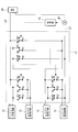
- FIG. 1 shows a schematic configuration of a power receiving device 1 applied to such a wireless power transmission system.
- the power receiving device 1 includes a plurality of antennas 11 and a plurality of rectenna rectifier circuits (rectifier units) 12 provided corresponding to the antennas 11.
- FIG. 1 illustrates the case where four antennas 11 and four rectenna rectifier circuits 12 are provided, but the number of antennas and the number of rectenna rectifier circuits 12 are not limited.
- FIG. 1 illustrates the case where a rectenna rectifier circuit 12 is provided corresponding to each antenna 11.
- a rectenna rectifier circuit 12 is provided for an antenna group including a plurality of antennas 11. May be provided.
- the rectenna rectifier circuit 12 includes, for example, a rectifier capacitor, a rectifier diode, and the like, and converts the electromagnetic wave received by the corresponding antenna 11 into DC power and outputs it.
- connection switching circuit 13 On the output side of the plurality of rectenna rectifier circuits 12, a connection switching circuit (connection switching unit) 13 that switches the series-parallel connection state on the output side of the plurality of rectenna rectifier circuits is provided.
- the connection switching circuit 13 includes a plurality of switching elements K ⁇ b> 1 and K ⁇ b> 2 connected to the output line of the rectenna rectifier circuit 12. By switching the switching elements K1 and K2, the connection state on the output side of the rectenna rectifier circuit 12 can be switched to three patterns of 4 parallel, 2 series 2 parallel, and 4 series.
- the output lines of the rectenna rectifier circuits 12 are connected to a common positive output line L1 and a negative output line L2 through a connection switching circuit 13, and through these output lines. Output power from the rectenna rectifier circuit 12 is supplied to the load 20.
- the positive output line L1 or the negative output L2 is provided with a current sensor (current measurement unit) 14 for measuring the current flowing through the load 20.
- the measurement current measured by the current sensor 14 is output to the control unit 15.
- the control unit 15 selects a series-parallel connection state of the rectenna rectifier circuit that maximizes the RF-DC conversion efficiency based on the measured current acquired from the current sensor 14 so that the selected series-parallel connection state is obtained.
- the connection switching circuit 13 is controlled.
- control unit 15 has information associating the measurement current with the series-parallel connection state in which optimum RF-DC conversion efficiency is obtained, and the measurement current measured by the current sensor 14 from the information.
- the connection switching circuit 13 is controlled so as to obtain the series-parallel connection state obtained.
- control unit 15 includes the first information associated with the input power, load resistance, and measurement current of the electromagnetic wave received by the plurality of receiving antennas 11, the input power of the electromagnetic wave, the load resistance, and the RF. -With second information associated with DC efficiency.
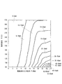
- Fig. 3 shows an example of the first information.
- the distribution of the output current (measurement current) I [mA] is shown on the coordinate axis with the horizontal axis indicating the input power P [dBm] of the electromagnetic wave and the vertical axis indicating the load resistance R [ ⁇ ].
- the output current I is shown in units of 5 mA, but this unit is not particularly limited.
- the current value without data may be obtained by interpolating existing data.
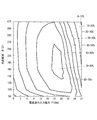
- FIG. 4 shows an example of the second information.
- the distribution of the RF-DC conversion efficiency ⁇ [%] is shown on the coordinate axis with the horizontal axis indicating the input power P [dBm] of the electromagnetic wave and the vertical axis indicating the load resistance R [ ⁇ ].
- the RF-DC conversion efficiency ⁇ is shown in units of 10%, but this unit is not particularly limited.
- the RF-DC conversion efficiency ⁇ with no data may be obtained by interpolating existing data.
- a maximum efficiency curve indicating the maximum RF-DC conversion efficiency may be obtained from the map shown in FIG. 4, and a characteristic formula of this maximum efficiency curve may be held as the second information.
- the control unit 15 acquires the input power of the electromagnetic wave corresponding to the measurement current and the current load resistance from the first information illustrated in FIG.
- the load resistance that provides the maximum RF-DC efficiency corresponding to the input power is obtained from the second information shown in FIG.
- switching element K1, K2 with which the connection switching circuit 13 is provided is switched so that it may become a serial parallel connection state from which the load resistance nearest to the acquired load resistance is obtained.
- the switches K1 and K2 of the connection switching circuit 13 are in the ON state. Therefore, the rectenna rectifier circuit 12 will be described assuming a case where four parallel connections are made on the output side.
- the electromagnetic waves received by the antennas 11 are converted into DC power by the corresponding rectenna rectifier circuits 12.
- This DC power is supplied to the load 20 via the output line of the rectenna rectifier circuit 12 and the common positive output line L1 and negative output line L2.
- the current sensor 14 measures the current current, and this measured current is output to the control unit 15.
- the control unit 15 acquires the input power of the electromagnetic wave corresponding to the measurement current by referring to the first information shown in FIG. 3 based on the input measurement current. Specifically, the control unit 15 calculates the load resistance for each rectenna rectifier circuit 12 from the current connection state (four parallel connection state) of the connection switching circuit 13 and the current value of the load 20. At this time, as the value of the load 20, a preset design value may be used, or the actual value of the load 20 may be measured and used.
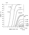
- the control unit 15 acquires the input power of the electromagnetic wave corresponding to the calculated load resistance and the measured current input from the current sensor 14 from the first information. For example, as shown in FIG. 6, when the calculated load resistance is 200 [ ⁇ ] and the measured current is 21 mA, 22 [dBm] is obtained as the input power of the electromagnetic wave.
- the control unit 15 acquires the load resistance R [ ⁇ ] that maximizes the RF-DC conversion efficiency corresponding to the input power of the electromagnetic wave obtained from FIG. 3 from the maximum efficiency curve shown in FIG. As a result, as shown in FIG. 7, 100 [ ⁇ ] is obtained as the load resistance that maximizes the RF-DC conversion efficiency at the electromagnetic wave input power of 22 [dBm].
- the control unit 15 considers the current value of the load 20 and selects the connection state in which the load resistance for each rectenna rectifier circuit 12 is closest to 100 [ ⁇ ] from among 4 parallel, 2 series, 2 parallel, and 4 series. Then, the switching elements K1 and K2 of the connection switching circuit 13 are controlled so that the selected connection state is obtained. As a result, the optimum load resistance for the current power receiving state can be selected, and the RF-DC conversion efficiency can be increased as much as possible.
- the connection state on the output side of the rectenna rectifier circuit 12 is changed with respect to the input power of the electromagnetic wave. Accordingly, the load resistance value for each rectenna rectifier circuit 12 can be apparently changed. Thereby, for example, even when the load 20 cannot be freely adjusted as in a commercial power system, the load resistance is such that the largest RF-DC conversion efficiency can be obtained with respect to the input power of the electromagnetic wave. Further, by changing the connection state on the output side of the rectenna rectifier circuit 12, it is possible to obtain the RF-DC conversion efficiency as much as possible.
- the control unit 15 holds the first information and the second information drawn as a map, and an optimum load resistance value corresponding to the input power of the electromagnetic wave is obtained based on the information.
- the connection switching circuit 13 is controlled based on the load resistance value. Instead, for example, the measurement current and the RF-CD conversion efficiency are maximized based on the first information and the second information.
- a correspondence table that directly associates the connection state of the rectenna rectifier circuit 12 is created in advance, and the output side connection state of the rectenna rectifier circuit is selected directly from the measured current based on the correspondence table. It is good. FIG.
- correspondence table that directly associates the measurement current with the connection state of the rectenna rectifier circuit that maximizes the RF-CD conversion efficiency.
- correspondence table for example, in the case of the first threshold value I 1 below measured current I is set in advance, switching elements K1 and K2 are in the ON state (4 parallel state) in the connection switching circuit 13 , the measurement current I is greater than the first threshold value I 1 which is set in advance, and when the second threshold value I 2 or less that is set in advance, the switching elements K1 in the connection switching circuit 13 is turned OFF, K2 There is an oN state (2 serial two-parallel state), when the measured current I is greater than the second threshold value I 2 which is set in advance, the switching elements K1 and K2 are in the OFF state (4 series state) .
- connection switching circuit 13 by controlling the connection switching circuit 13 using the correspondence table that directly associates the measurement current with the connection state of the rectenna rectifier circuit 12 that maximizes the RF-CD conversion efficiency, Compared to the case of using the map or the like, the processing can be reduced and the time can be shortened.
Landscapes
- Engineering & Computer Science (AREA)
- Computer Networks & Wireless Communication (AREA)
- Power Engineering (AREA)
- Dc-Dc Converters (AREA)
- Rectifiers (AREA)
Abstract
入力電力が変動する場合であってもRF-DC変換効率の向上を図ること。複数のアンテナ(11)と、各アンテナ(11)に対応してそれぞれ設けられ、対応するアンテナ(11)によって受信された電磁波を直流電力に変換して出力する複数のレクテナ整流回路(12)と、複数のレクテナ整流回路(12)と負荷(20)との間に設けられ、複数のレクテナ整流回路(12)の出力側の直並列接続状態を切り替える接続切替回路(13)と、負荷(20)に流れる電流を計測する電流センサ(14)と、電流センサ(14)によって計測された計測電流に基づいて、RF-DC変換効率が最大となるようなレクテナ整流回路(12)の直並列接続状態を選択し、選択した直並列接続状態となるように接続切替回路(13)を制御する制御部(15)とを具備する受電装置(1)を提供する。
Description
本発明は、例えば、宇宙空間に巨大な太陽電池パネルを広げ、発生した電力をマイクロ波で地上に送信するようにした宇宙太陽発電システムに用いられる受電装置に関するものである。
近年、化石燃料の利用による二酸化炭素排出量の増加に伴い、地球温暖化などの環境問題や化石燃料枯渇などのエネルギー問題がクローズアップされている。このためクリーンエネルギーの需要は年々高まっており、それらの問題に対する解決方法の一つとして宇宙太陽発電システム(SSPS:Space Solar Power System)計画が挙げられている。
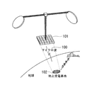
SSPS計画とは、図9に示すように、巨大な太陽電池パネルを搭載した人工衛星を赤道上空に打ち上げ、太陽光によって発電した電力を太陽電池パネルの中の送電モジュールによりマイクロ波に変換する。そして、マイクロ波100をマイクロ波送電部101から地上に設けた地上受電基地102へ送電し、地上において再び電力に変換して利用するという計画である。
SSPS計画とは、図9に示すように、巨大な太陽電池パネルを搭載した人工衛星を赤道上空に打ち上げ、太陽光によって発電した電力を太陽電池パネルの中の送電モジュールによりマイクロ波に変換する。そして、マイクロ波100をマイクロ波送電部101から地上に設けた地上受電基地102へ送電し、地上において再び電力に変換して利用するという計画である。
これにより太陽発電の欠点である天候や時間帯に左右されること無く、クリーンなエネルギーを安定して供給することができる。この計画の実現のためには、大電力送電、マイクロ波ビーム制御、運用コストの低減などが技術課題として挙げられ、それらを満足させるための様々な技術の一つとして、地上受電基地102におけるRF-DC変換効率の向上が挙げられる(例えば、特許文献1参照)。
上述したような電力をマイクロ波等の電磁波に変換して送電し、これを受電して電力を取り出すような無線電力伝送システムにおいて、受電装置におけるRF-DC変換効率を向上させるためには、一般的に、レクテナ(電磁波を直流電力に変換するRF-DC変換素子)の後段に、入力電力の設計値に対するRF-DC変換効率を最大とするような抵抗値を持つ抵抗を接続することが知られている。
しかしながら、無線電力伝送システムでは、電磁波の送電状況等によって受電の電波状態が変わるため、レクテナへ入力される電力は変動し、必ずしも設計値で一定とはならない。
RF-DC変換効率を最大とする抵抗値は入力電力に応じて変化するため、設計値に合わせて抵抗値を決定してしまうと、受電状況によってはRF-DC変換効率が大幅に低減してしまうおそれがある。
RF-DC変換効率を最大とする抵抗値は入力電力に応じて変化するため、設計値に合わせて抵抗値を決定してしまうと、受電状況によってはRF-DC変換効率が大幅に低減してしまうおそれがある。
無線電力伝送システムでは、レクテナから出力される電力を商用電力系統に供給する場合があり、この場合には、商用電力系統の負荷がレクテナ後段の負荷となる。しかしながら、商用電力系統の負荷はユーザ側で決められるものであり、この負荷値を自由に変更することはできない。このため、RF-DC変換効率を最大とする負荷を選択することができず、RF-DC変換効率を向上させることができなかった。
本発明は、このような事情に鑑みてなされたものであって、入力電力が変動する場合であってもRF-DC変換効率の向上を図ることのできる受電装置及び無線電力伝送システムを提供することを目的とする。
上記課題を解決するために、本発明は以下の部を採用する。
本発明の一態様は、複数のアンテナと、1または複数の前記アンテナに対応してそれぞれ設けられ、対応する前記アンテナによって受信された電磁波を直流電力に変換して出力する複数の整流部と、複数の前記整流部と負荷との間に設けられ、複数の前記整流部の出力側の直並列接続状態を切り替える接続切替部と、前記負荷に流れる電流を計測する電流計測部と、前記電流計測部によって計測された計測電流に基づいて、RF-DC変換効率が最大となるような前記整流部の直並列接続状態を選択し、選択した直並列接続状態となるように前記接続切替部を制御する制御部とを具備する受電装置を提供する。
本発明の一態様は、複数のアンテナと、1または複数の前記アンテナに対応してそれぞれ設けられ、対応する前記アンテナによって受信された電磁波を直流電力に変換して出力する複数の整流部と、複数の前記整流部と負荷との間に設けられ、複数の前記整流部の出力側の直並列接続状態を切り替える接続切替部と、前記負荷に流れる電流を計測する電流計測部と、前記電流計測部によって計測された計測電流に基づいて、RF-DC変換効率が最大となるような前記整流部の直並列接続状態を選択し、選択した直並列接続状態となるように前記接続切替部を制御する制御部とを具備する受電装置を提供する。
このような構成によれば、各アンテナによって受信された電磁波は、そのアンテナに対応する整流部にそれぞれ出力され、整流部によって直流電力に変換される。整流部から出力された直流電力は、接続切替部を介して負荷に供給される。この場合において、整流部の出力側における直並列接続状態は、接続切替部によって切替可能とされており、また、制御部が、負荷に流れる電流に基づいてRF-DC変換効率が最大となるような整流部の出力側の直並列接続状態となるように、接続切替部を制御する。これにより、例えば、負荷が商用電力系統のように、その値を自由に変更できないような場合であっても、各整流部に対する見かけ上の負荷を、RF-DC変換効率が最適となるように変化させることができる。これにより、入力される電磁波の状況が変化したとしても、その変化に追従してRF-DC変換効率が高まる方向へ負荷を調整することが可能となる。
上記受電装置において、前記制御部は、計測電流と最大のRF-DC変換効率が得られる直並列接続状態とを関連付けた情報を有しており、前記情報から前記電流計測部によって計測された計測電流に対する直並列接続状態を取得し、取得した直並列接続状態となるように前記接続切替部を制御することとしてもよい。
このように、負荷に流れる計測電流と最大のRF-DC変換効率が得られる整流部の直並列接続状態とを関連付けた情報を有しており、この情報に基づいて整流部の直並列接続状態を制御するので、容易にRF-DC変換効率を向上させることができる。
上記受電装置において、前記制御部は、複数の前記受信アンテナによって受電される電磁波の入力電力と、負荷抵抗と、計測電流とを関連付けた第1情報と、前記電磁波の入力電力と、負荷抵抗と、RF-DC効率とを関連付けた第2情報とを有し、現在の負荷抵抗と計測電流とに対応する電磁波の入力電力を前記第1情報から取得し、取得した電磁波の入力電力に対応する最大のRF-DC効率が得られる負荷抵抗を前記第2情報から取得し、取得した負荷抵抗に最も近い負荷抵抗が得られる直並列接続状態となるように前記接続切替部を切り替えることとしてもよい。
このように、制御部が第1情報及び第2情報を用いて制御切替部を制御するので、容易にRF-DC変換効率を向上させることができる。
上記受電装置は、例えば、太陽光発電衛星から地上受電設備に向けてマイクロ波等の電磁波により電力を地上に送電する宇宙太陽発電システムや、地上の電力供給施設から有線による電力供給が難しい構造物(例えば、船舶、飛行機、飛行船)等に対して電磁波を用いて電力を供給するシステム等のように、電力を電磁波として送信し、これを受信して電力に変換する無線電力伝送システムに適用されて好適な装置である。
本発明によれば、入力電力が変動する場合であってもRF-DC変換効率の向上を図ることができるという効果を奏する。
以下に、本発明の一実施形態に係る受電装置及び無線電力伝送システムについて、図面を参照して説明する。
本発明の一実施形態に係る無線電力伝送システムは、例えば、太陽光発電衛星から地上受電設備に向けてマイクロ波等の電磁波により電力を地上に送電する宇宙太陽発電システムや、地上の電力供給施設から有線による電力供給が難しい構造物(例えば、船舶、飛行機、飛行船)等に対して電磁波を用いて電力を供給するシステム等のように、電力を電磁波として送信する送電装置と、送電装置から送信された電磁波を受信して電力に変換する受電装置とを備えている。
本発明の一実施形態に係る無線電力伝送システムは、例えば、太陽光発電衛星から地上受電設備に向けてマイクロ波等の電磁波により電力を地上に送電する宇宙太陽発電システムや、地上の電力供給施設から有線による電力供給が難しい構造物(例えば、船舶、飛行機、飛行船)等に対して電磁波を用いて電力を供給するシステム等のように、電力を電磁波として送信する送電装置と、送電装置から送信された電磁波を受信して電力に変換する受電装置とを備えている。
図1に、このような無線電力伝送システムに適用される受電装置1の概略構成を示す。図1に示すように、受電装置1は、複数のアンテナ11と、各アンテナ11に対応して設けられた複数のレクテナ整流回路(整流部)12とを備えている。
図1では、4つのアンテナ11と、4つのレクテナ整流回路12とを備えている場合について例示しているが、アンテナの設置数およびレクテナ整流回路12の設置数は限定されない。図1では、各アンテナ11に対応してそれぞれレクテナ整流回路12が設けられている場合を例示しているが、例えば、複数のアンテナ11から構成されるアンテナ群に対して1つのレクテナ整流回路12が設けられていてもよい。
レクテナ整流回路12は、例えば、整流コンデンサ、整流ダイオード等を備えており、対応するアンテナ11によって受信された電磁波を直流電力に変換して出力する。
複数のレクテナ整流回路12の出力側には、複数のレクテナ整流回路の出力側の直並列接続状態を切り替える接続切替回路(接続切替部)13が設けられている。接続切替回路13は、図2に示すように、レクテナ整流回路12の出力線に接続された複数のスイッチング素子K1、K2を有している。このスイッチング素子K1、K2を切り替えることにより、レクテナ整流回路12の出力側の接続状態を4並列、2直2並列、4直列の3パターンに切り替えることができる。具体的には、スイッチング素子K1及びK2をON側に接続した場合には4並列状態、スイッチK1をON側に、スイッチK2をOFF側に接続した場合には2直2並列状態、スイッチK1及びK2をOFF側に接続した場合には4直列状態となる。本実施形態では、上記3パターンの切り替えが可能とされているが、接続切替回路13を更に複雑な構成とすることで、3直2並列についても可能とすることができる。
図1、図2に示されるように、各レクテナ整流回路12の出力線は、接続切替回路13を介して共通の正極出力線L1及び負極出力線L2に接続され、これらの出力線を介してレクテナ整流回路12からの出力電力が負荷20へ供給される。
正極出力線L1または負極出力L2には、負荷20に流れる電流を計測するための電流センサ(電流計測部)14が設けられている。電流センサ14によって計測された計測電流は、制御部15に出力される。制御部15は、電流センサ14から取得した計測電流に基づいて、RF-DC変換効率が最大となるようなレクテナ整流回路の直並列接続状態を選択し、選択した直並列接続状態となるように接続切替回路13を制御する。このように、各レクテナ整流回路の直並列接続状態を変えることで、負荷20の値を直接的に変えずに、各レクテナ整流回路12に対する負荷の見かけ上の値を変化させることが可能となる。
具体的には、制御部15は、計測電流と最適なRF-DC変換効率が得られる直並列接続状態とを関連付けた情報を有しており、該情報から電流センサ14によって計測された計測電流に対する直並列接続状態を取得し、取得した直並列接続状態となるように接続切替回路13を制御する。
より具体的には、制御部15は、複数の受信アンテナ11によって受電される電磁波の入力電力、負荷抵抗、及び計測電流が関連付けられた第1情報と、電磁波の入力電力、負荷抵抗、及びRF-DC効率が関連付けられた第2情報とを有している。
図3に第1情報の一例を示す。図3には、横軸に電磁波の入力電力P[dBm]、縦軸に負荷抵抗R[Ω]が示された座標軸上に出力電流(計測電流)I[mA]の分布が示されている。図3において、出力電流Iは5mA単位で示されているが、この単位は特に限定されない。データがない電流値については、存在するデータを補間することにより求めることとしてもよい。更に、図3に示したようなマップとしてではなく、関係演算式として保有していてもよい。
図4に、第2情報の一例を示す。図4には、横軸に電磁波の入力電力P[dBm]、縦軸に負荷抵抗R[Ω]が示された座標軸上にRF-DC変換効率η[%]の分布が示されている。図4において、RF-DC変換効率ηは10%単位で示されているが、この単位は特に限定されない。データがないRF-DC変換効率ηについては、存在するデータを補間することにより求めることとしてもよい。更に、図4に示したようなマップとしてではなく、関係演算式として保有していてもよい。図5に示すように、図4に示したマップから最大のRF-DC変換効率を示す最大効率曲線を求め、この最大効率曲線の特性式を第2情報として保有していてもよい。
制御部15は、電流センサ14から計測電流が入力されると、この計測電流と現在の負荷抵抗とに対応する電磁波の入力電力を図3に示した第1情報から取得し、取得した電磁波の入力電力に対応する最大のRF-DC効率が得られる負荷抵抗を図4に示した第2情報から取得する。そして、取得した負荷抵抗に最も近い負荷抵抗が得られる直並列接続状態となるように接続切替回路13が備えるスイッチング素子K1、K2を切り替える。
次に、上述した構成を備える本実施形態に係る受電装置の作用について説明する。ここでは、説明の便宜上、接続切替回路13のスイッチK1、K2はON状態とされている。したがって、レクテナ整流回路12はその出力側において4並列接続されている場合を想定して説明する。
受電装置1において、各アンテナ11により受信された電磁波は、それぞれ対応するレクテナ整流回路12によって直流電力に変換される。この直流電力は、レクテナ整流回路12の出力線及び共通の正極出力線L1及び負極出力線L2を介して負荷20へ供給される。また、電流センサ14によって現在の電流が計測され、この計測電流が制御部15へ出力される。
制御部15は、入力された計測電流に基づいて図3に示した第1情報を参照することにより、計測電流に対応する電磁波の入力電力を取得する。具体的には、制御部15は、現在の接続切替回路13の接続状態(4並列接続状態)と現在の負荷20の値とから、各レクテナ整流回路12に対する負荷抵抗を算出する。このとき、負荷20の値は、予め設定した設計値を用いてもよいし、実際の負荷20の値を計測し、その値を用いることとしてもよい。
続いて、制御部15は、算出した負荷抵抗と電流センサ14から入力された計測電流とに対応する電磁波の入力電力を第1情報から取得する。例えば、図6に示すように、算出した負荷抵抗が200[Ω]、計測電流が21mAであった場合には、電磁波の入力電力として22[dBm]が得られる。
続いて、制御部15は、図3から得られた電磁波の入力電力に対応し、RF-DC変換効率が最大となる負荷抵抗R[Ω]を図5に示した最大効率曲線から取得する。この結果、図7に示すように、電磁波の入力電力22[dBm]において最もRF-DC変換効率が最大となる負荷抵抗として、100[Ω]が得られる。制御部15は、現在の負荷20の値を考慮して、各レクテナ整流回路12に対する負荷抵抗が100[Ω]に最も近くなる接続状態を4並列、2直2並列、4直列の中から選択し、選択した接続状態となるように、接続切替回路13のスイッチング素子K1,K2を制御する。これにより、現在の受電状態に最適な負荷抵抗が選択でき、RF-DC変換効率を可能な限り高めることができる。
以上、説明してきたように、本実施形態に係る受電装置及び無線電力伝送システムによれば、レクテナ整流回路12の出力側における接続状態を電磁波の入力電力に対して変化させるので、電磁波の入力電力に応じて、各レクテナ整流回路12に対する負荷抵抗値を見かけ上変化させることが可能となる。これにより、例えば、負荷20が商用電力系統のように自由に調整できないような場合であっても、電磁波の入力電力に対して最も大きなRF-DC変換効率が得られるような負荷抵抗となるようにレクテナ整流回路12の出力側の接続状態を変えることで、可能な限りのRF-DC変換効率を得ることが可能となる。
〔変形例1〕
上述した実施形態では、例えば、マップとして描かれた第1情報、第2情報を制御部15が保有しており、これらの情報に基づいて電磁波の入力電力に応じた最適な負荷抵抗値を求め、この負荷抵抗値に基づいて接続切替回路13を制御することとしたが、これに代えて、例えば、第1情報、第2情報に基づいて、計測電流とRF-CD変換効率が最大となるようなレクテナ整流回路12の接続状態とを直接的に対応付けた対応テーブルを予め作成しておき、この対応テーブルに基づいて計測電流から直接的にレクテナ整流回路の出力側接続状態を選択することとしてもよい。図8に計測電流とRF-CD変換効率が最大となるようなレクテナ整流回路の接続状態とを直接的に対応付けた対応テーブルの一例を示す。このような対応テーブルにおいては、例えば、計測電流Iが予め設定されている第1閾値I1以下の場合には、接続切替回路13におけるスイッチング素子K1及びK2がON状態(4並列状態)とされ、計測電流Iが予め設定されている第1閾値I1よりも大きく、かつ、予め設定されている第2閾値I2以下の場合には、接続切替回路13におけるスイッチング素子K1がOFF状態、K2がON状態(2直2並列状態)とされ、計測電流Iが予め設定されている第2閾値I2よりも大きい場合には、スイッチング素子K1及びK2がOFF状態(4直列状態)とされる。
上述した実施形態では、例えば、マップとして描かれた第1情報、第2情報を制御部15が保有しており、これらの情報に基づいて電磁波の入力電力に応じた最適な負荷抵抗値を求め、この負荷抵抗値に基づいて接続切替回路13を制御することとしたが、これに代えて、例えば、第1情報、第2情報に基づいて、計測電流とRF-CD変換効率が最大となるようなレクテナ整流回路12の接続状態とを直接的に対応付けた対応テーブルを予め作成しておき、この対応テーブルに基づいて計測電流から直接的にレクテナ整流回路の出力側接続状態を選択することとしてもよい。図8に計測電流とRF-CD変換効率が最大となるようなレクテナ整流回路の接続状態とを直接的に対応付けた対応テーブルの一例を示す。このような対応テーブルにおいては、例えば、計測電流Iが予め設定されている第1閾値I1以下の場合には、接続切替回路13におけるスイッチング素子K1及びK2がON状態(4並列状態)とされ、計測電流Iが予め設定されている第1閾値I1よりも大きく、かつ、予め設定されている第2閾値I2以下の場合には、接続切替回路13におけるスイッチング素子K1がOFF状態、K2がON状態(2直2並列状態)とされ、計測電流Iが予め設定されている第2閾値I2よりも大きい場合には、スイッチング素子K1及びK2がOFF状態(4直列状態)とされる。
このように、計測電流とRF-CD変換効率が最大となるようなレクテナ整流回路12の接続状態とを直接的に対応付けた対応テーブルを用いて、接続切替回路13を制御することにより、上記のマップ等を使用する場合に比べ、処理の軽減、時間短縮を図ることが可能となる。
1 受電装置
11 アンテナ
12 レクテナ整流回路
13 接続切替回路
14 電流センサ
15 制御部
20 負荷
11 アンテナ
12 レクテナ整流回路
13 接続切替回路
14 電流センサ
15 制御部
20 負荷
Claims (4)
- 複数のアンテナと、
1または複数の前記アンテナに対応してそれぞれ設けられ、対応する前記アンテナによって受信された電磁波を直流電力に変換して出力する複数の整流部と、
複数の前記整流部と負荷との間に設けられ、複数の前記整流部の出力側の直並列接続状態を切り替える接続切替部と、
前記負荷に流れる電流を計測する電流計測部と、
前記電流計測部によって計測された計測電流に基づいて、RF-DC変換効率が最大となるような前記整流部の直並列接続状態を選択し、選択した直並列接続状態となるように前記接続切替部を制御する制御部と
を具備する受電装置。 - 前記制御部は、計測電流と最大のRF-DC変換効率が得られる直並列接続状態とを関連付けた情報を有しており、前記情報から前記電流計測部によって計測された計測電流に対する直並列接続状態を取得し、取得した直並列接続状態となるように前記接続切替部を制御する請求項1に記載の受電装置。
- 前記制御部は、
複数の前記受信アンテナによって受電される電磁波の入力電力と、負荷抵抗と、計測電流とを関連付けた第1情報と、
前記電磁波の入力電力と、負荷抵抗と、RF-DC効率とを関連付けた第2情報と
を有し、
現在の負荷抵抗と計測電流とに対応する電磁波の入力電力を前記第1情報から取得し、取得した電磁波の入力電力に対応する最大のRF-DC効率が得られる負荷抵抗を前記第2情報から取得し、取得した負荷抵抗に最も近い負荷抵抗が得られる直並列接続状態となるように前記接続切替部を切り替える請求項1に記載の受電装置。 - 請求項1から請求項3のいずれか一項に記載の受電装置を有する無線電力伝送システム。
Priority Applications (1)
| Application Number | Priority Date | Filing Date | Title |
|---|---|---|---|
| US13/387,500 US9287717B2 (en) | 2009-11-26 | 2010-11-24 | Power receiving device and wireless power transmission system |
Applications Claiming Priority (2)
| Application Number | Priority Date | Filing Date | Title |
|---|---|---|---|
| JP2009-269197 | 2009-11-26 | ||
| JP2009269197A JP5419650B2 (ja) | 2009-11-26 | 2009-11-26 | 受電装置及び無線電力伝送システム |
Publications (1)
| Publication Number | Publication Date |
|---|---|
| WO2011065352A1 true WO2011065352A1 (ja) | 2011-06-03 |
Family
ID=44066457
Family Applications (1)
| Application Number | Title | Priority Date | Filing Date |
|---|---|---|---|
| PCT/JP2010/070871 Ceased WO2011065352A1 (ja) | 2009-11-26 | 2010-11-24 | 受電装置及び無線電力伝送システム |
Country Status (3)
| Country | Link |
|---|---|
| US (1) | US9287717B2 (ja) |
| JP (1) | JP5419650B2 (ja) |
| WO (1) | WO2011065352A1 (ja) |
Cited By (4)
| Publication number | Priority date | Publication date | Assignee | Title |
|---|---|---|---|---|
| US8933589B2 (en) | 2012-02-07 | 2015-01-13 | The Gillette Company | Wireless power transfer using separately tunable resonators |
| CN105119387A (zh) * | 2015-08-27 | 2015-12-02 | 西安空间无线电技术研究所 | 一种基于能量分布特性的提高能量传输效率的系统及方法 |
| US10574094B2 (en) | 2017-04-13 | 2020-02-25 | Kabushiki Kaisha Toyota Chuo Kenkyusho | Transmitter and microwave power transmission system |
| US12531411B2 (en) | 2022-03-31 | 2026-01-20 | Softbank Corp. | Switching circuit, DC power output apparatus, wireless power transmission system, solar power generation system, output control method and program |
Families Citing this family (14)
| Publication number | Priority date | Publication date | Assignee | Title |
|---|---|---|---|---|
| US10523276B2 (en) * | 2011-08-16 | 2019-12-31 | Qualcomm Incorporated | Wireless power receiver with multiple receiver coils |
| JP2014176170A (ja) * | 2013-03-07 | 2014-09-22 | Toshiba Corp | 受電装置および充電システム |
| KR102391190B1 (ko) | 2015-03-13 | 2022-04-28 | 삼성전자주식회사 | 무선 충전 시스템에서 무선 전력 수신기의 로드 생성 방법 및 무선 전력 수신기 |
| GB201518859D0 (en) * | 2015-10-23 | 2015-12-09 | Airbus Defence & Space Ltd | High-efficiency amplifier |
| JP6691394B2 (ja) * | 2016-02-29 | 2020-04-28 | 日本電信電話株式会社 | レクテナアレー |
| KR102686599B1 (ko) * | 2016-08-23 | 2024-07-22 | 삼성전자주식회사 | 전력 제공 장치 및 전력을 수신하는 전자 장치와 그 제어 방법 |
| JP6972349B2 (ja) * | 2018-07-18 | 2021-11-24 | 三菱電機株式会社 | レクテナ制御器及びそれを備えたレクテナ装置 |
| US12081046B2 (en) * | 2021-01-19 | 2024-09-03 | Datalogic IP Tech, S.r.l. | Apparatus for dynamic control of wireless power transfer |
| TWI785680B (zh) * | 2021-07-14 | 2022-12-01 | 元太科技工業股份有限公司 | 射頻整流器電路及電子紙顯示裝置 |
| US12603527B2 (en) | 2021-12-28 | 2026-04-14 | Sony Semiconductor Solutions Corporation | Energy collection device and rectifier circuit |
| WO2023181359A1 (ja) * | 2022-03-25 | 2023-09-28 | Tdk株式会社 | レクテナ装置 |
| BG67724B1 (bg) * | 2022-04-29 | 2025-05-15 | Иван Игнатов Михайлов | Наноелектронна система за охлаждане на процесори и ram памети |
| JP2024085833A (ja) * | 2022-12-15 | 2024-06-27 | 株式会社東芝 | 無線電力受電装置、無線電力伝送システム及び無線電力受電方法 |
| JP7557004B1 (ja) * | 2023-04-25 | 2024-09-26 | ソフトバンク株式会社 | 電力供給システム及び無線電力伝送システム |
Citations (2)
| Publication number | Priority date | Publication date | Assignee | Title |
|---|---|---|---|---|
| WO2007048052A2 (en) * | 2005-10-21 | 2007-04-26 | The Regents Of The University Of Colorado | Systems and methods for receiving and managing power in wireless devices |
| JP2009038924A (ja) * | 2007-08-02 | 2009-02-19 | Kyoto Univ | 無線電力受電アダプタ |
Family Cites Families (8)
| Publication number | Priority date | Publication date | Assignee | Title |
|---|---|---|---|---|
| JPH0833243A (ja) * | 1994-07-18 | 1996-02-02 | Nissan Motor Co Ltd | マイクロ波受電装置 |
| JPH1146451A (ja) * | 1997-07-24 | 1999-02-16 | Sekisui Jushi Co Ltd | 太陽電池式電源装置 |
| JP3485445B2 (ja) * | 1997-07-24 | 2004-01-13 | 積水樹脂株式会社 | 太陽電池式電源装置 |
| JP2003309938A (ja) * | 2002-04-15 | 2003-10-31 | Mitsubishi Electric Corp | 宇宙太陽光発電システム、携行型小電力電子機器、受信アンテナ装置及び電力システム |
| WO2005104331A1 (ja) | 2004-03-30 | 2005-11-03 | Mitsubishi Denki Kabushiki Kaisha | レクテナ太陽電池ハイブリッドパネル、及びハイブリッド太陽光発電システム |
| JP2008199857A (ja) * | 2007-02-15 | 2008-08-28 | Fujifilm Corp | レクテナ装置 |
| JP2009065726A (ja) * | 2007-09-04 | 2009-03-26 | Fujifilm Corp | レクテナ装置 |
| JP2009278782A (ja) * | 2008-05-15 | 2009-11-26 | Nissan Diesel Motor Co Ltd | マイクロ波受電システム |
-
2009
- 2009-11-26 JP JP2009269197A patent/JP5419650B2/ja not_active Expired - Fee Related
-
2010
- 2010-11-24 US US13/387,500 patent/US9287717B2/en not_active Expired - Fee Related
- 2010-11-24 WO PCT/JP2010/070871 patent/WO2011065352A1/ja not_active Ceased
Patent Citations (2)
| Publication number | Priority date | Publication date | Assignee | Title |
|---|---|---|---|---|
| WO2007048052A2 (en) * | 2005-10-21 | 2007-04-26 | The Regents Of The University Of Colorado | Systems and methods for receiving and managing power in wireless devices |
| JP2009038924A (ja) * | 2007-08-02 | 2009-02-19 | Kyoto Univ | 無線電力受電アダプタ |
Cited By (6)
| Publication number | Priority date | Publication date | Assignee | Title |
|---|---|---|---|---|
| US8933589B2 (en) | 2012-02-07 | 2015-01-13 | The Gillette Company | Wireless power transfer using separately tunable resonators |
| US9634495B2 (en) | 2012-02-07 | 2017-04-25 | Duracell U.S. Operations, Inc. | Wireless power transfer using separately tunable resonators |
| CN105119387A (zh) * | 2015-08-27 | 2015-12-02 | 西安空间无线电技术研究所 | 一种基于能量分布特性的提高能量传输效率的系统及方法 |
| CN105119387B (zh) * | 2015-08-27 | 2017-08-29 | 西安空间无线电技术研究所 | 一种基于能量分布特性的提高能量传输效率的系统及方法 |
| US10574094B2 (en) | 2017-04-13 | 2020-02-25 | Kabushiki Kaisha Toyota Chuo Kenkyusho | Transmitter and microwave power transmission system |
| US12531411B2 (en) | 2022-03-31 | 2026-01-20 | Softbank Corp. | Switching circuit, DC power output apparatus, wireless power transmission system, solar power generation system, output control method and program |
Also Published As
| Publication number | Publication date |
|---|---|
| JP5419650B2 (ja) | 2014-02-19 |
| US9287717B2 (en) | 2016-03-15 |
| US20120133216A1 (en) | 2012-05-31 |
| JP2011114949A (ja) | 2011-06-09 |
Similar Documents
| Publication | Publication Date | Title |
|---|---|---|
| JP5419650B2 (ja) | 受電装置及び無線電力伝送システム | |
| CN102598472B (zh) | 发电系统及发电单元 | |
| US9130389B2 (en) | Apparatus for wireless power transmission using multi antenna and method for controlling the same | |
| Agamy et al. | An efficient partial power processing DC/DC converter for distributed PV architectures | |
| US20100277001A1 (en) | Systems, Methods, and Apparatus for Converting DC Power to AC Power | |
| WO2013116289A1 (en) | Techniques for grid coupling photovoltaic cells using ratiometric voltage conversion | |
| KR20130124772A (ko) | 전력변환 시스템 및 전력변환 방법과, 그 시스템을 제어하는 장치 및 방법 | |
| CN101860088A (zh) | 用于飞艇的微波无线传能系统 | |
| KR20160077933A (ko) | 웨어러블 기기의 무선 충전 장치 및 시스템 | |
| US11764611B2 (en) | Low gain wireless power transfer system and method | |
| US10284115B2 (en) | Inverter system | |
| CN102111087A (zh) | 智能虚拟低电压光伏模块和使用其的光伏电力系统 | |
| CN107658900B (zh) | 光伏并网系统 | |
| WO2018126551A1 (zh) | 光伏阵列的最大功率点跟踪控制系统及光伏空调系统 | |
| US20130234524A1 (en) | Control method for arranging dc/ac converters in parallel | |
| US11038373B2 (en) | Power transmission system including power transmitter apparatus, power receiver apparatus, or power transmitter and receiver apparatus easily attachable and detachable to/from transmission path | |
| WO2020186708A1 (zh) | 一种数字无线检测变换器及输电线路监测设备 | |
| KR20170008901A (ko) | 광대역 전자기파를 포집 및 이용하는 에너지 하베스팅 시스템 | |
| JP2015192549A (ja) | 電力変換装置及び電力変換方法 | |
| CN104734177B (zh) | 并网连接设备及其控制方法和并网供电系统 | |
| CN203895990U (zh) | 光伏并网系统 | |
| EP4593277A1 (en) | Power conversion system and ripple current suppression method therefor | |
| Dong et al. | A dual-active single-ended wireless v2h system with mutually synchronized phase-difference control method | |
| CN203632269U (zh) | 并网连接设备和并网供电系统 | |
| JP2014090633A (ja) | 非接触電力伝送装置 |
Legal Events
| Date | Code | Title | Description |
|---|---|---|---|
| 121 | Ep: the epo has been informed by wipo that ep was designated in this application |
Ref document number: 10833198 Country of ref document: EP Kind code of ref document: A1 |
|
| WWE | Wipo information: entry into national phase |
Ref document number: 13387500 Country of ref document: US |
|
| NENP | Non-entry into the national phase |
Ref country code: DE |
|
| 122 | Ep: pct application non-entry in european phase |
Ref document number: 10833198 Country of ref document: EP Kind code of ref document: A1 |