WO2011064993A1 - 受光素子の作製方法、受光素子作製装置 - Google Patents
受光素子の作製方法、受光素子作製装置 Download PDFInfo
- Publication number
- WO2011064993A1 WO2011064993A1 PCT/JP2010/006858 JP2010006858W WO2011064993A1 WO 2011064993 A1 WO2011064993 A1 WO 2011064993A1 JP 2010006858 W JP2010006858 W JP 2010006858W WO 2011064993 A1 WO2011064993 A1 WO 2011064993A1
- Authority
- WO
- WIPO (PCT)
- Prior art keywords
- light
- type semiconductor
- receiving element
- local
- light receiving
- Prior art date
- Legal status (The legal status is an assumption and is not a legal conclusion. Google has not performed a legal analysis and makes no representation as to the accuracy of the status listed.)
- Ceased
Links
Images




Classifications
-
- H—ELECTRICITY
- H10—SEMICONDUCTOR DEVICES; ELECTRIC SOLID-STATE DEVICES NOT OTHERWISE PROVIDED FOR
- H10F—INORGANIC SEMICONDUCTOR DEVICES SENSITIVE TO INFRARED RADIATION, LIGHT, ELECTROMAGNETIC RADIATION OF SHORTER WAVELENGTH OR CORPUSCULAR RADIATION
- H10F71/00—Manufacture or treatment of devices covered by this subclass
-
- C—CHEMISTRY; METALLURGY
- C23—COATING METALLIC MATERIAL; COATING MATERIAL WITH METALLIC MATERIAL; CHEMICAL SURFACE TREATMENT; DIFFUSION TREATMENT OF METALLIC MATERIAL; COATING BY VACUUM EVAPORATION, BY SPUTTERING, BY ION IMPLANTATION OR BY CHEMICAL VAPOUR DEPOSITION, IN GENERAL; INHIBITING CORROSION OF METALLIC MATERIAL OR INCRUSTATION IN GENERAL
- C23C—COATING METALLIC MATERIAL; COATING MATERIAL WITH METALLIC MATERIAL; SURFACE TREATMENT OF METALLIC MATERIAL BY DIFFUSION INTO THE SURFACE, BY CHEMICAL CONVERSION OR SUBSTITUTION; COATING BY VACUUM EVAPORATION, BY SPUTTERING, BY ION IMPLANTATION OR BY CHEMICAL VAPOUR DEPOSITION, IN GENERAL
- C23C14/00—Coating by vacuum evaporation, by sputtering or by ion implantation of the coating forming material
- C23C14/22—Coating by vacuum evaporation, by sputtering or by ion implantation of the coating forming material characterised by the process of coating
- C23C14/34—Sputtering
- C23C14/3435—Applying energy to the substrate during sputtering
-
- H—ELECTRICITY
- H10—SEMICONDUCTOR DEVICES; ELECTRIC SOLID-STATE DEVICES NOT OTHERWISE PROVIDED FOR
- H10K—ORGANIC ELECTRIC SOLID-STATE DEVICES
- H10K30/00—Organic devices sensitive to infrared radiation, light, electromagnetic radiation of shorter wavelength or corpuscular radiation
- H10K30/10—Organic devices sensitive to infrared radiation, light, electromagnetic radiation of shorter wavelength or corpuscular radiation comprising heterojunctions between organic semiconductors and inorganic semiconductors
-
- H—ELECTRICITY
- H10—SEMICONDUCTOR DEVICES; ELECTRIC SOLID-STATE DEVICES NOT OTHERWISE PROVIDED FOR
- H10P—GENERIC PROCESSES OR APPARATUS FOR THE MANUFACTURE OR TREATMENT OF DEVICES COVERED BY CLASS H10
- H10P14/00—Formation of materials, e.g. in the shape of layers or pillars
- H10P14/20—Formation of materials, e.g. in the shape of layers or pillars of semiconductor materials
-
- H—ELECTRICITY
- H10—SEMICONDUCTOR DEVICES; ELECTRIC SOLID-STATE DEVICES NOT OTHERWISE PROVIDED FOR
- H10P—GENERIC PROCESSES OR APPARATUS FOR THE MANUFACTURE OR TREATMENT OF DEVICES COVERED BY CLASS H10
- H10P14/00—Formation of materials, e.g. in the shape of layers or pillars
- H10P14/20—Formation of materials, e.g. in the shape of layers or pillars of semiconductor materials
- H10P14/22—Formation of materials, e.g. in the shape of layers or pillars of semiconductor materials using physical deposition, e.g. vacuum deposition or sputtering
-
- H—ELECTRICITY
- H10—SEMICONDUCTOR DEVICES; ELECTRIC SOLID-STATE DEVICES NOT OTHERWISE PROVIDED FOR
- H10P—GENERIC PROCESSES OR APPARATUS FOR THE MANUFACTURE OR TREATMENT OF DEVICES COVERED BY CLASS H10
- H10P14/00—Formation of materials, e.g. in the shape of layers or pillars
- H10P14/20—Formation of materials, e.g. in the shape of layers or pillars of semiconductor materials
- H10P14/29—Formation of materials, e.g. in the shape of layers or pillars of semiconductor materials characterised by the substrates
- H10P14/2901—Materials
-
- H—ELECTRICITY
- H10—SEMICONDUCTOR DEVICES; ELECTRIC SOLID-STATE DEVICES NOT OTHERWISE PROVIDED FOR
- H10P—GENERIC PROCESSES OR APPARATUS FOR THE MANUFACTURE OR TREATMENT OF DEVICES COVERED BY CLASS H10
- H10P14/00—Formation of materials, e.g. in the shape of layers or pillars
- H10P14/20—Formation of materials, e.g. in the shape of layers or pillars of semiconductor materials
- H10P14/34—Deposited materials, e.g. layers
- H10P14/3402—Deposited materials, e.g. layers characterised by the chemical composition
-
- H—ELECTRICITY
- H10—SEMICONDUCTOR DEVICES; ELECTRIC SOLID-STATE DEVICES NOT OTHERWISE PROVIDED FOR
- H10K—ORGANIC ELECTRIC SOLID-STATE DEVICES
- H10K30/00—Organic devices sensitive to infrared radiation, light, electromagnetic radiation of shorter wavelength or corpuscular radiation
- H10K30/50—Photovoltaic [PV] devices
-
- Y—GENERAL TAGGING OF NEW TECHNOLOGICAL DEVELOPMENTS; GENERAL TAGGING OF CROSS-SECTIONAL TECHNOLOGIES SPANNING OVER SEVERAL SECTIONS OF THE IPC; TECHNICAL SUBJECTS COVERED BY FORMER USPC CROSS-REFERENCE ART COLLECTIONS [XRACs] AND DIGESTS
- Y02—TECHNOLOGIES OR APPLICATIONS FOR MITIGATION OR ADAPTATION AGAINST CLIMATE CHANGE
- Y02E—REDUCTION OF GREENHOUSE GAS [GHG] EMISSIONS, RELATED TO ENERGY GENERATION, TRANSMISSION OR DISTRIBUTION
- Y02E10/00—Energy generation through renewable energy sources
- Y02E10/50—Photovoltaic [PV] energy
- Y02E10/549—Organic PV cells
-
- Y—GENERAL TAGGING OF NEW TECHNOLOGICAL DEVELOPMENTS; GENERAL TAGGING OF CROSS-SECTIONAL TECHNOLOGIES SPANNING OVER SEVERAL SECTIONS OF THE IPC; TECHNICAL SUBJECTS COVERED BY FORMER USPC CROSS-REFERENCE ART COLLECTIONS [XRACs] AND DIGESTS
- Y02—TECHNOLOGIES OR APPLICATIONS FOR MITIGATION OR ADAPTATION AGAINST CLIMATE CHANGE
- Y02P—CLIMATE CHANGE MITIGATION TECHNOLOGIES IN THE PRODUCTION OR PROCESSING OF GOODS
- Y02P70/00—Climate change mitigation technologies in the production process for final industrial or consumer products
- Y02P70/50—Manufacturing or production processes characterised by the final manufactured product
Definitions
- the present invention relates to a light receiving element manufacturing method, and more particularly to a light receiving element manufacturing method and a light receiving element manufacturing apparatus capable of easily manufacturing an element having sensitivity to a specific wavelength without selecting a material.
- the light receiving element receives light in a state where a depletion layer is formed by applying a reverse bias voltage to the PN junction.
- Light incident on the light receiving surface of the light receiving element is absorbed in a region having a small energy band called a light absorbing layer, and carriers are generated in the light absorbing layer.
- Carriers generated by light absorption are accelerated by an internal electric field gradient based on the applied reverse bias voltage and detected as an electric signal.
- the wavelength region where the light receiving sensitivity can be given is limited due to the limitation of the material technology.
- Non-Patent Document 1 a technique for detecting only near-field light having no sensitivity to propagating light using a non-adiabatic process using near-field light has been proposed.
- the technique of Non-Patent Document 1 described above does not focus on how easily an element having sensitivity to a specific wavelength can be produced without selecting a material.
- the present invention has been devised in view of the above-described problems, and the object of the present invention is to easily select an element having sensitivity to a specific wavelength without selecting a material.
- An object of the present invention is to provide a light receiving element manufacturing method and a light receiving element manufacturing apparatus.
- a method for manufacturing a light receiving element according to claim 1 of the present invention is connected to a PN junction obtained by bonding a P-type semiconductor and an N-type semiconductor, and to the P-type semiconductor and the N-type semiconductor, respectively.
- a material constituting any one of the P-type semiconductor, the N-type semiconductor, and the electrodes is applied with a reverse bias voltage, and the absorption wavelength of the material to be deposited
- the irradiated light of the desired wavelength is absorbed through a non-adiabatic process by the near-field light generated in the local shape to generate electrons, and the generated electrons
- Non-adiabatic flow that continuously cancels the occurrence of the local electric field based on the reverse bias voltage in the place shape, and the place where the local electric field based on the reverse bias voltage occurs in the place where the local shape is not formed
- Particles constituting the material are sequentially adsorbed, and when the local shape is formed through the adsorption process, the particle adsorbing flow moves to the non-adiabatic flow.
- the method for producing a light receiving element according to claim 2 of the present application is the invention according to claim 1, wherein the non-adiabatic flow and the particle adsorption flow are continuously performed, whereby the local surface is deposited on the surface of the deposited material. It is characterized in that the shape is sequentially formed.
- the light receiving element according to claim 3 of the present application is manufactured by the method for manufacturing a light receiving element according to claim 1 or 2.
- a light receiving element manufacturing apparatus manufactures a light receiving element having a PN junction obtained by bonding a P-type semiconductor and an N-type semiconductor, and each electrode connected to the P-type semiconductor and the N-type semiconductor.
- the material constituting any one of the P-type semiconductor, the N-type semiconductor, and the electrodes is longer than the voltage application means for applying a reverse bias voltage and the absorption wavelength of the material to be deposited.
- the irradiation light of the desired wavelength is absorbed through the non-adiabatic process by the near-field light generated in the local shape to generate electrons, and the generated electrons generate the electrons.
- a non-adiabatic flow that continuously cancels the occurrence of a local electric field based on the reverse bias voltage in the shape, and the location where the local electric field based on the reverse bias voltage is generated at a location where the local shape is not formed.
- the particles constituting the material are sequentially adsorbed, and when the local shape is formed through the adsorption process, a particle adsorption flow that moves to the non-adiabatic flow is executed.
- an element having sensitivity to a specific wavelength can be easily manufactured without selecting a material.
- FIG. 1 shows a configuration of a sputtering apparatus 3 for realizing a light receiving element manufacturing method to which the present invention is applied.
- the light receiving element 1 In the sputtering apparatus 3, the light receiving element 1, a base 32 for installing the light receiving element 1, a target 34 disposed on the side facing the light receiving element 1, and the target 34 are mounted.
- the power supply 36 is provided outside the chamber 31 and connected to the electrode 35, and the optical oscillator 37 is provided on the side of the chamber 31. Composed.
- an inert gas such as Ar is introduced, and a voltage is applied to the electrodes by the power source 36 to discharge.
- a plasma state can be created in the vicinity of the surface of the target 34. Since the potential of the generated plasma is usually higher than the surface of the target 34, a DC electric field is generated between the plasma and the target 34. Positive ions such as Ar + in the inert gas are accelerated by the generated electric field and collide with the surface of the target 34.
- sputtering occurs, so that fine particles on the target 34 are sequentially emitted. Incidentally, the emitted fine particles are deposited on the light receiving element 1 without colliding with molecules of the inert gas.
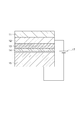
- FIG. 2 shows a detailed configuration of the light receiving element 1 actually installed on the table 32.
- the light receiving element includes a first electrode 12 stacked on a substrate 11, an N-type semiconductor 13 connected to the first electrode 2, a P-type semiconductor 14 forming a PN junction with the N-type semiconductor 13, And a second electrode 15 connected to the P-type semiconductor 14.
- a power source 17 is connected to the first electrode 12 and the second electrode 15, and a reverse bias voltage is loaded so that the N-type side is a positive voltage and the P-type side is a negative voltage.
- the substrate 11 is formed of a so-called sapphire, silicon substrate, or the like.
- the first electrode 12 is composed of a transparent electrode or the like, and for example, ITO (Indium Tin Oxide) may be used.
- ITO Indium Tin Oxide
- Ag or the like may be used for the second electrode 15.
- the first electrode 12 and the second electrode 15 are not limited to these, and any material may be used.
- the N-type semiconductor 13 for example, a semiconductor represented by ZnO, In 2 O 3 , SnO 2 or the like may be used.
- the P-type semiconductor 14 polythiophene (P3HT) or the like may be used.
- the N-type semiconductor 13 and the P-type semiconductor 14 constituting the PN junction are not limited to these, and any material may be used.
- the power source 17 is composed of a stabilized DC power source, a battery, and the like.
- the material constituting any of the P-type semiconductor 14, the N-type semiconductor 13, and the electrodes 12 and 15 is deposited by sputtering.
- this deposition step light having a wavelength longer than the absorption wavelength of the material to be deposited is applied to the optical oscillator 37 while applying a reverse bias voltage to the PN junction composed of the P-type semiconductor 14 and the N-type semiconductor 13 described above. Is emitted.
- the light emitted from the optical oscillator 37 is guided onto the light receiving element 1 through the window 31a.
- the wavelength of the light emitted from the optical oscillator 37 is referred to as a desired wavelength.
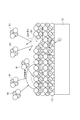
- FIG. 3 shows a microscopic state of the material surface when the material constituting the N-type semiconductor 13 is deposited by sputtering.
- a local electric field based on the reverse bias voltage is generated on the surface of the N-type semiconductor 13.
- the particles 51 constituting the material of the N-type semiconductor 13 are sequentially adsorbed at the location where the local electric field is generated. Through this adsorption process, materials are sequentially deposited on the surface of the N-type semiconductor 13.
- the flow in which the particles 51 are sequentially adsorbed to the local electric field is referred to as a particle adsorption flow.
- the local shape 54 shown in FIG. 3 may be formed by chance.
- the local shape 54 is a shape that can generate near-field light more effectively when the above-described light having the desired wavelength is irradiated.
- the local shape 54 that can generate this near-field light varies depending on the wavelength of the irradiated light. For this reason, when the desired wavelength is changed, the local shape 54 that can generate near-field light is naturally different. That is, the local shape 54 is unique for each desired wavelength.
- the local shape 54 capable of effectively generating near-field light with respect to the desired wavelength to be irradiated this time is a shape as shown in FIG. 3, the local shape 54 is temporarily formed in another location. Therefore, near-field light based on the desired wavelength is generated in the same manner.
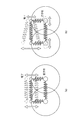
- FIG. 4 shows a conceptual diagram of the potential energy of the material of the N-type semiconductor 13. It is stable in a state where the internuclear distance of the atoms constituting the material of the N-type semiconductor 13 is kept constant. However, photon energy excites electrons in the molecular orbitals.
- This non-adiabatic process can be thought of as a model in which bonds between atoms are replaced with springs, as shown in FIG.
- the wavelength of propagating light is much larger than the size of the molecule, so it can be regarded as a spatially uniform electric field at the molecular level.
- adjacent electrons are vibrated with the same amplitude and the same phase by the spring. Since the atomic nucleus of the photosensitive resin film 12 is heavy, it cannot follow the vibration of the electrons, and the molecular vibration is hardly caused in the propagating light. In this way, in propagation light, it can be ignored that molecular vibrations are involved in the excitation process of electrons, so this process is called an adiabatic process (see Non-Patent Document 1).
- the spatial electric field gradient of near-field light decreases very steeply. For this reason, near-field light gives different vibrations to adjacent electrons, and as shown in FIG. 5B, heavy nuclei are also vibrated by the vibrations of the different electrons.
- energy corresponds to the form of molecular vibration. Therefore, in near-field light, as shown in FIG. 4, an excitation process (non-adiabatic process) via a vibration level occurs. It becomes possible.
- the excitation process via the vibration level of the nucleus is called a non-adiabatic process because the nucleus moves in response to the adiabatic process that is a normal optical response (see Non-Patent Document 1).
- the non-adiabatic process electrons are excited through vibration levels as shown in FIG. 4, so that even a light having a wavelength longer than the absorption wavelength of the material to be deposited can be excited to an excited state. Electrons can be generated.
- the local shape 54 is excited to an excited state based on a non-adiabatic process.
- this non-adiabatic process even light of low energy, that is, light having a desired wavelength that is longer than the absorption wavelength of the material to be deposited can be excited by the excitation process via the vibration level described above.
- electrons can be selectively generated only for the local shape 54.
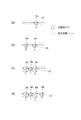
- a flow in which electrons are generated in the local shape 54 through a non-adiabatic process based on such near-field light and a local electric field is generated in the local shape 54 based on the generated electrons is hereinafter referred to as a non-adiabatic flow.
- a non-adiabatic flow is continuously generated in the local shape 54, and electrons are continuously generated in the local shape 54.
- the generation of a local electric field in the local shape 54 is always canceled by the electrons.
- the local shape 54 can prevent the particles 51 constituting the material of the N-type semiconductor 13 from being adsorbed. It becomes possible. As a result, the local shape 54 is not adsorbed by the particles 51, and the shape is maintained until the deposition process is completed.
- the method of manufacturing the light receiving element to which the present invention is applied allows the local shape 54 to be sequentially formed on the surface of the deposited material by continuously executing the non-adiabatic flow and the particle adsorption flow described above. To do.
- the local shape 54 is sequentially formed on the surface of the deposited material.
- a large number of local shapes 54 are formed on the surface of the N-type semiconductor 13 where the deposition process is finally completed.
- the first electrode 12 and the second electrode 15 have a positive voltage on the N-type side.
- the reverse bias voltage is loaded so that the P-type side becomes a negative voltage, and the depletion layer formed in the PN junction is irradiated with light to be received.
- near-field light is generated in the local shape 54 when light having a desired wavelength is incident. This is because the local shape 54 can generate near-field light more effectively when irradiated with light of a desired wavelength, as described above.
- a light receiving element having sensitivity to a specific wavelength when it is desired to manufacture a light receiving element having sensitivity to a specific wavelength, by irradiating light having the specific wavelength as a desired wavelength, A light receiving element capable of receiving light of the desired wavelength can be manufactured. Therefore, according to the present invention, an element having sensitivity to a specific wavelength can be easily manufactured without selecting a material.
- FIG. 8 shows the wavelength dependence with respect to the photocurrent of the light receiving element 1 manufactured through the method for manufacturing the light receiving element to which the present invention is applied.
- Each plot is an example when the light intensity of incident light is 0.1 mW, 0.5 mW, and 1.0 mW, respectively.
- the horizontal axis represents wavelength and the vertical axis represents photocurrent.
- the peak of the received photocurrent was 620 nm.
- near-field light is generated in the local shape 54 and a non-adiabatic process occurs, and light of a desired wavelength having a wavelength of 660 nm is received as light on a low wavelength side centering on the wavelength of 620 nm. Can do.
- the present invention is not limited to this, and other P-type semiconductors 14, the respective electrodes 12, The same technical idea can be applied when depositing 15.
- MBE Molecular Beam Epitaxy
- CVD Chemical Vapor Deposition
Landscapes
- Chemical & Material Sciences (AREA)
- Chemical Kinetics & Catalysis (AREA)
- Engineering & Computer Science (AREA)
- Materials Engineering (AREA)
- Mechanical Engineering (AREA)
- Metallurgy (AREA)
- Organic Chemistry (AREA)
- Inorganic Chemistry (AREA)
- Physics & Mathematics (AREA)
- Electromagnetism (AREA)
- Light Receiving Elements (AREA)
- Electroluminescent Light Sources (AREA)
Abstract
Description
3 スパッタリング装置
11 基板
12 第1の電極
13 N型半導体
14 P型半導体
15 第2の電極
17 電源
31 チャンバ
32 台
34 ターゲット
35 電極
36 電源
37 光発振器
51 粒子
54 局所形状
Claims (4)
- P型半導体とN型半導体とを接合したPN接合と、上記P型半導体並びにN型半導体にそれぞれ接続された各電極とを有する受光素子の作製方法において、
上記P型半導体、上記N型半導体、上記各電極の何れかを構成する材料を、逆バイアス電圧を印加するとともに、堆積させる材料の吸収波長よりも長波長である希望波長の光を照射しつつ堆積させる堆積工程を有し、
上記堆積工程は、
上記希望波長の照射光により近接場光を発生可能な局所形状が上記堆積させている材料表面に形成されている箇所では、当該局所形状に発生した近接場光による非断熱過程を通じて上記希望波長の照射光を光吸収して電子を生成するとともに、その生成した電子により当該局所形状に上記逆バイアス電圧に基づく局所電場が生じるのを打ち消すことを連続して行う非断熱フローと、
上記局所形状が未形成の箇所では、上記逆バイアス電圧に基づく局所電場が生じた箇所に上記材料を構成する粒子を順次吸着させ、その吸着プロセスを経て上記局所形状が形成された場合には上記非断熱フローへ移行する粒子吸着フローとを有すること
を特徴とする受光素子の作製方法。 - 上記非断熱フローと上記粒子吸着フローとを継続して実行することにより、上記堆積させている材料表面に上記局所形状を順次形成させていくこと
を特徴とする請求項1記載の受光素子の作製方法。 - 請求項1又は2記載の受光素子の作製方法により作製されたことを特徴とする受光素子。
- P型半導体とN型半導体とを接合したPN接合と、上記P型半導体並びにN型半導体にそれぞれ接続された各電極とを有する受光素子を作製するための受光素子作製装置において、
上記P型半導体、上記N型半導体、上記各電極の何れかを構成する材料を、逆バイアス電圧を印加する電圧印加手段と、
堆積させる材料の吸収波長よりも長波長である希望波長の光を照射しつつ堆積させる堆積手段とを有し、
上記堆積手段は、
上記希望波長の照射光により近接場光を発生可能な局所形状が上記堆積させている材料表面に形成されている箇所では、当該局所形状に発生した近接場光による非断熱過程を通じて上記希望波長の照射光を光吸収して電子を生成するとともに、その生成した電子により当該局所形状に上記逆バイアス電圧に基づく局所電場が生じるのを打ち消すことを連続して行う非断熱フローと、
上記局所形状が未形成の箇所では、上記逆バイアス電圧に基づく局所電場が生じた箇所に上記材料を構成する粒子を順次吸着させ、その吸着プロセスを経て上記局所形状が形成された場合には上記非断熱フローへ移行する粒子吸着フローとを実行すること
を特徴とする受光素子作製装置。
Priority Applications (3)
| Application Number | Priority Date | Filing Date | Title |
|---|---|---|---|
| CN201080035324.9A CN102473791B (zh) | 2009-11-25 | 2010-11-24 | 受光元件的制作方法、受光元件制作装置 |
| DE112010004544T DE112010004544T5 (de) | 2009-11-25 | 2010-11-24 | Verfahren zur Herstellung eines Lichtaufnahmeelements und Vorrichtung zur Herstellung des Lichtaufnahmeelements |
| US13/511,734 US20130009193A1 (en) | 2009-11-25 | 2010-11-24 | Method of fabricating light receiving element and apparatus for fabricating light receiving element |
Applications Claiming Priority (2)
| Application Number | Priority Date | Filing Date | Title |
|---|---|---|---|
| JP2009267811A JP5209592B2 (ja) | 2009-11-25 | 2009-11-25 | 受光素子の作製方法 |
| JP2009-267811 | 2009-11-25 |
Publications (1)
| Publication Number | Publication Date |
|---|---|
| WO2011064993A1 true WO2011064993A1 (ja) | 2011-06-03 |
Family
ID=44066101
Family Applications (1)
| Application Number | Title | Priority Date | Filing Date |
|---|---|---|---|
| PCT/JP2010/006858 Ceased WO2011064993A1 (ja) | 2009-11-25 | 2010-11-24 | 受光素子の作製方法、受光素子作製装置 |
Country Status (5)
| Country | Link |
|---|---|
| US (1) | US20130009193A1 (ja) |
| JP (1) | JP5209592B2 (ja) |
| CN (1) | CN102473791B (ja) |
| DE (1) | DE112010004544T5 (ja) |
| WO (1) | WO2011064993A1 (ja) |
Cited By (1)
| Publication number | Priority date | Publication date | Assignee | Title |
|---|---|---|---|---|
| JP2012169565A (ja) * | 2011-02-16 | 2012-09-06 | Optoelectronics Industry And Technology Development Association | 受光素子の作製方法 |
Families Citing this family (4)
| Publication number | Priority date | Publication date | Assignee | Title |
|---|---|---|---|---|
| JP5946278B2 (ja) * | 2012-01-18 | 2016-07-06 | 特定非営利活動法人ナノフォトニクス工学推進機構 | 被加工体の熱加工方法 |
| JP6073599B2 (ja) * | 2012-08-24 | 2017-02-01 | 特定非営利活動法人ナノフォトニクス工学推進機構 | エレクトロルミネッセンス素子の作製方法 |
| JP6100200B2 (ja) * | 2014-04-24 | 2017-03-22 | 信越半導体株式会社 | 貼り合わせsoiウェーハの製造方法 |
| JP6529048B2 (ja) * | 2017-09-22 | 2019-06-12 | 株式会社ソディック | 発光デバイスの製造方法 |
Citations (2)
| Publication number | Priority date | Publication date | Assignee | Title |
|---|---|---|---|---|
| JP2004277813A (ja) * | 2003-03-14 | 2004-10-07 | Japan Science & Technology Agency | 薄膜の作製方法、並びに微粒子の堆積方法 |
| JP2009094345A (ja) * | 2007-10-10 | 2009-04-30 | Univ Of Tokyo | 表面平坦化方法 |
-
2009
- 2009-11-25 JP JP2009267811A patent/JP5209592B2/ja not_active Expired - Fee Related
-
2010
- 2010-11-24 WO PCT/JP2010/006858 patent/WO2011064993A1/ja not_active Ceased
- 2010-11-24 CN CN201080035324.9A patent/CN102473791B/zh not_active Expired - Fee Related
- 2010-11-24 US US13/511,734 patent/US20130009193A1/en not_active Abandoned
- 2010-11-24 DE DE112010004544T patent/DE112010004544T5/de not_active Withdrawn
Patent Citations (2)
| Publication number | Priority date | Publication date | Assignee | Title |
|---|---|---|---|---|
| JP2004277813A (ja) * | 2003-03-14 | 2004-10-07 | Japan Science & Technology Agency | 薄膜の作製方法、並びに微粒子の堆積方法 |
| JP2009094345A (ja) * | 2007-10-10 | 2009-04-30 | Univ Of Tokyo | 表面平坦化方法 |
Non-Patent Citations (1)
| Title |
|---|
| SOTARO YUKITAKE ET AL.: "Hi Dannetsu Katei ni Motozuku Hacho Sentakusei o Yusuru Koden Henkan Soshi no Kaihatsu", EXTENDED ABSTRACTS, JAPAN SOCIETY OF APPLIED PHYSICS AND RELATED SOCIETIES, 57TH, 2010, pages 18A - 4-13 * |
Cited By (1)
| Publication number | Priority date | Publication date | Assignee | Title |
|---|---|---|---|---|
| JP2012169565A (ja) * | 2011-02-16 | 2012-09-06 | Optoelectronics Industry And Technology Development Association | 受光素子の作製方法 |
Also Published As
| Publication number | Publication date |
|---|---|
| US20130009193A1 (en) | 2013-01-10 |
| CN102473791B (zh) | 2014-10-08 |
| JP2011114076A (ja) | 2011-06-09 |
| JP5209592B2 (ja) | 2013-06-12 |
| DE112010004544T5 (de) | 2012-12-06 |
| CN102473791A (zh) | 2012-05-23 |
Similar Documents
| Publication | Publication Date | Title |
|---|---|---|
| Guo et al. | Refining the substrate surface morphology for achieving efficient inverted perovskite solar cells | |
| Widmann et al. | Electrical charge state manipulation of single silicon vacancies in a silicon carbide quantum optoelectronic device | |
| Hou et al. | Concurrent inhibition and redistribution of spontaneous emission from all inorganic perovskite photonic crystals | |
| Li et al. | High performance photodetector based on 2D CH3NH3PbI3 perovskite nanosheets | |
| Nguyen et al. | Efficient radiative and nonradiative energy transfer from proximal CdSe/ZnS nanocrystals into silicon nanomembranes | |
| Qian et al. | Ultra‐Sensitive β‐Ga2O3 Solar‐Blind Photodetector with High‐Density Al@ Al2O3 Core− Shell Nanoplasmonic Array | |
| Karbalaei Akbari et al. | ALD-developed plasmonic two-dimensional Au–WO3–TiO2 heterojunction architectonics for design of photovoltaic devices | |
| JP5209592B2 (ja) | 受光素子の作製方法 | |
| Al Amin et al. | Achieving a highly stable perovskite photodetector with a long lifetime fabricated via an all-vacuum deposition process | |
| Wyrsch et al. | Review of amorphous silicon based particle detectors: the quest for single particle detection | |
| CN103178150A (zh) | 天线耦合太赫兹探测器 | |
| Shaheen et al. | Spatiotemporal observation of electron-impact dynamics in photovoltaic materials using 4D electron microscopy | |
| Lu et al. | Localized surface plasmon enhanced photoresponse of AlGaN MSM solar-blind ultraviolet photodetectors | |
| Lin et al. | Packaging glass with a hierarchically nanostructured surface: a universal method to achieve self-cleaning omnidirectional solar cells | |
| Guo et al. | Surface/interface carrier-transport modulation for constructing photon-alternative ultraviolet detectors based on self-bending-assembled ZnO nanowires | |
| Xi et al. | Plasmonic resonance enabling 2D perovskite single crystal to detect telecommunication light | |
| Li et al. | Beating the Responsivity‐Speed Trade‐Off in Asymmetric GaN‐Based UV Photodetectors: A Novel van der Waals Metal Contact Approach | |
| Wang et al. | Back-reflected performance-enhanced flexible perovskite photodetectors through substrate texturing with femtosecond laser | |
| Mortazavifar et al. | Ultra-thin broadband solar absorber based on stadium-shaped silicon nanowire arrays | |
| Xu et al. | Narrow-band solar-blind ultraviolet detectors based on AlSnO films with tunable band gap | |
| Cai et al. | Ultrahigh Sensitivity Solar‐Blind UV Detection via Multistage‐Concentric‐Annulus Architecture Metasurface | |
| Hötger et al. | Photovoltage and photocurrent absorption spectra of sulfur vacancies locally patterned in monolayer MoS2 | |
| Nekita et al. | Diffusion-dominated luminescence dynamics of CsPbBr3 studied using cathodoluminescence and microphotoluminescence spectroscopy | |
| Wang et al. | Computational discovery of intermolecular singlet fission materials using many-body perturbation theory | |
| Razeen et al. | Enhanced Performance of Metal‐Semiconductor‐Metal UV Photodetectors on Algan/Gan Hemt Structure via Periodic Nanohole Patterning |
Legal Events
| Date | Code | Title | Description |
|---|---|---|---|
| WWE | Wipo information: entry into national phase |
Ref document number: 201080035324.9 Country of ref document: CN |
|
| 121 | Ep: the epo has been informed by wipo that ep was designated in this application |
Ref document number: 10832843 Country of ref document: EP Kind code of ref document: A1 |
|
| WWE | Wipo information: entry into national phase |
Ref document number: 1120100045445 Country of ref document: DE Ref document number: 112010004544 Country of ref document: DE |
|
| WWE | Wipo information: entry into national phase |
Ref document number: 13511734 Country of ref document: US |
|
| 122 | Ep: pct application non-entry in european phase |
Ref document number: 10832843 Country of ref document: EP Kind code of ref document: A1 |