WO2011049083A1 - 座標入力装置 - Google Patents
座標入力装置 Download PDFInfo
- Publication number
- WO2011049083A1 WO2011049083A1 PCT/JP2010/068380 JP2010068380W WO2011049083A1 WO 2011049083 A1 WO2011049083 A1 WO 2011049083A1 JP 2010068380 W JP2010068380 W JP 2010068380W WO 2011049083 A1 WO2011049083 A1 WO 2011049083A1
- Authority
- WO
- WIPO (PCT)
- Prior art keywords
- contact
- contact group
- counter electrode
- electrode
- substrate
- Prior art date
- Legal status (The legal status is an assumption and is not a legal conclusion. Google has not performed a legal analysis and makes no representation as to the accuracy of the status listed.)
- Ceased
Links
Images






Classifications
-
- G—PHYSICS
- G06—COMPUTING OR CALCULATING; COUNTING
- G06F—ELECTRIC DIGITAL DATA PROCESSING
- G06F3/00—Input arrangements for transferring data to be processed into a form capable of being handled by the computer; Output arrangements for transferring data from processing unit to output unit, e.g. interface arrangements
- G06F3/01—Input arrangements or combined input and output arrangements for interaction between user and computer
- G06F3/03—Arrangements for converting the position or the displacement of a member into a coded form
- G06F3/033—Pointing devices displaced or positioned by the user, e.g. mice, trackballs, pens or joysticks; Accessories therefor
- G06F3/0338—Pointing devices displaced or positioned by the user, e.g. mice, trackballs, pens or joysticks; Accessories therefor with detection of limited linear or angular displacement of an operating part of the device from a neutral position, e.g. isotonic or isometric joysticks
-
- H—ELECTRICITY
- H01—ELECTRIC ELEMENTS
- H01H—ELECTRIC SWITCHES; RELAYS; SELECTORS; EMERGENCY PROTECTIVE DEVICES
- H01H2203/00—Form of contacts
- H01H2203/02—Interspersed fingers
-
- H—ELECTRICITY
- H01—ELECTRIC ELEMENTS
- H01H—ELECTRIC SWITCHES; RELAYS; SELECTORS; EMERGENCY PROTECTIVE DEVICES
- H01H25/00—Switches with compound movement of handle or other operating part
- H01H25/04—Operating part movable angularly in more than one plane, e.g. joystick
- H01H25/041—Operating part movable angularly in more than one plane, e.g. joystick having a generally flat operating member depressible at different locations to operate different controls
Definitions
- the present invention relates to a coordinate input device used for a portable terminal or the like.
- a so-called multi-directional key which has a plurality of contact points in the east, west, south, and north directions and detects an input vector by turning the contacts on and off. 1) is known.
- This method is easy to detect, but has a problem that the detection accuracy of the vector direction depends on the number of contacts, and the size is difficult to detect.
- Patent Document 2 and Patent Document 3 are known that combine a fixed contact with a movable contact made of pressure-sensitive conductive rubber and detect an input vector in an analog manner.
- an expensive pressure-sensitive conductive rubber must be used, and after determining the conduction resistance of each contact, an input vector must be calculated from the coordinate data of the contact on the substrate.
- Patent Document 4 a detection method for measuring the resistance ratio of two pressure-sensitive resistance elements has been proposed, but a dedicated detection circuit must also be prepared, and other on- In addition to an off-type input device, a pressure-sensitive resistance element must be formed by screen printing, which takes time and effort to manage this load-resistance characteristic.
- the coordinates obtained are in the same circular shape as the contact arrangement unless any correction is made.
- the east, west, north, and south directions are the vertices. Since it is a rhombus, some correction was required to match the rectangular display screen.
- touch panels for detecting the position touched on the display screen by an LCD or CRT are provided.
- a touch panel a resistive film type is often used, and interface devices for this resistive film type are in circulation.
- the present invention can use an existing interface, uses an inexpensive conductive rubber contact, and easily outputs a rectangular coordinate similar to a display screen used for a portable device or the like depending on the configuration of the contact.
- An object is to provide a coordinate input device that can be obtained.
- an XY orthogonal coordinate system is set on the main surface, and the first Y-direction contact group and the first Y-direction contact group arranged opposite to each other in the Y direction across the origin.
- the group has two contact points that face each other across the Y axis, and the X direction first contact group and the X direction second contact group each have two contact points that face each other across the X axis.
- the first contact group in the Y direction, the second contact group in the Y direction, the first contact group in the X direction, and the second contact group in the X direction each have a first electrode and a second electrode.
- a second substrate displaceable with respect to the first substrate, the Y-direction first counter electrode, the Y-direction second counter electrode, and the X-direction first electrode.
- an existing interface can be used, an inexpensive conductive rubber contact is used, and, depending on the configuration of the contact, rectangular coordinate output similar to that of a display screen used for a portable device or the like can be easily performed. Can get to.
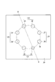
- FIG. 1 is a diagram illustrating an example of contact arrangement of the coordinate input device according to the first embodiment.
- an XY orthogonal coordinate system is set in the main surface of the flat insulating first substrate 10, and the Y-direction first contact groups 11 and 12 that face each other across the origin O in the Y direction and the Y direction. Second contact groups 13 and 14 are formed. Further, X-direction first contact groups 15 and 16 and X-direction second contact groups 17 and 18 that face each other across the origin O in the X direction are formed.
- the Y-direction first contact groups 11 and 12 are composed of a Y-direction first contact 11 and a Y-direction second contact 12 facing each other across the Y-axis, and the Y-direction second contact groups 13 and 14 sandwich the Y-axis.
- the Y-direction third contact 13 and the Y-direction fourth contact 14 are opposed to each other.
- the X-direction first contact groups 15 and 16 are composed of an X-direction first contact 15 and an X-direction second contact 16 facing each other with the X-axis interposed therebetween, and the X-direction second contact groups 17 and 18 sandwich the X-axis.
- the X-direction third contact 17 and the X-direction fourth contact 18 are opposed to each other.
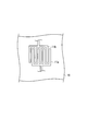
- FIG. 2 is a diagram showing the Y-direction first contact 11.
- the first contact 11 in the Y direction is formed in a comb-teeth shape and includes a first electrode 11a and a second electrode 11b arranged so as to be fitted to each other.
- the other contacts 12 to 18 are also configured in the same shape.
- Such a comb-shaped electrode has good pressure-sensitive characteristics by accurately detecting the area of the counter electrode described later.
- contacts 11 to 18 of the present embodiment are not limited to the comb-teeth shape, and may be configured as other shapes such as electrodes extending in parallel.
- the four contacts 14 form a quadrangular shape 1 such as a rectangle.
- These Y direction first contact groups 11 and 12 and Y direction second contact groups 13 and 14 constitute a Y direction press detecting means.
- the X direction first contact 15 and the X direction second contact 16 of the X direction first contact group 15, 16, and the X direction third contact 17 and the X direction fourth contact of the X direction second contact group 17, 18. 18 also constitutes a square shape 2 such as a rectangle.
- These X direction first contact groups 15 and 16 and the X direction second contact groups 17 and 18 constitute an X direction press detecting means.
- the Y direction first to fourth contacts 11 to 14 and the X direction first to fourth contacts 15 to 18 are located on the circumference 3 equidistant from the origin O.
- the Y direction first to fourth contacts 11 to 14 and the X direction first to fourth contacts 15 to 18 are not limited to the circumference 3 but may be located on the ellipse circumference.
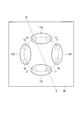
- FIG. 3 is a diagram showing the arrangement of the counter electrodes provided on the second substrate facing the first substrate.
- the second substrate 20 is disposed at a predetermined distance so as to be displaceable facing the first substrate 10.
- a Y-direction first counter electrode 121 having an electrode 21 and a second counter electrode 22 is provided, and a third counter facing the Y-direction third contact 13 and the Y-direction fourth contact 14 of the Y-direction second contact group 13, 14.
- a Y-direction second counter electrode 122 having an electrode 23 and a fourth counter electrode 24 is provided.
- an X-direction first counter electrode 123 having a fifth counter electrode 25 and a sixth counter electrode 26 facing the X-direction first contact 15 and the X-direction second contact 16 of the X-direction first contact group 15, 16 is provided.
- the X-direction second counter electrode 124 having the seventh counter electrode 27 and the eighth counter electrode 28 facing the X-direction third contact 17 and the X-direction fourth contact 18 of the X-direction second contact group 17, 18 is provided. It has been.
- the first to eighth counter electrodes 21 to 28 constituting these counter electrodes 121 to 124 are molded into a substantially spherical shape by so-called conductive rubber in which carbon-based, silver-based, or other conductive particles are blended with, for example, silicon rubber. Has been.
- this conductive rubber in addition to what is called a pressure-sensitive conductive grade, an inexpensive conductive rubber used for a general on-off switch can be used.
- FIG. 4 is a diagram showing another aspect of the arrangement of the counter electrodes provided on the second substrate facing the first substrate.
- the present embodiment is not limited to the configuration shown in FIG. 3, and the Y-direction first counter electrode 121, the Y-direction second counter electrode 122, the X-direction first counter electrode 123, and the X-direction second counter electrode 124 are included. It can also be configured as a single electrode.
- a Y-direction first counter electrode 121 facing the Y-direction first contact groups 11, 12 of the first substrate 10 is provided, and the Y-direction second contact group 13. , 14 is provided in the Y direction second counter electrode 122.
- an X-direction first counter electrode 123 facing the X-direction first contact groups 15 and 16 is provided, and an X-direction second counter electrode 124 facing the X-direction second contact groups 17 and 18 is provided.
- FIG. 5 is a diagram showing resistance characteristics against the pressing load of the conductive rubber.
- Curve a in the figure shows the characteristics of the pressure-sensitive conductive grade conductive rubber. Such conductive rubber, resistance decreases as the pressing load increases, asymptotically approaches a constant stable resistance R ON.
- Curve b in the figure shows the characteristics of the conductive rubber used for the on-off switch. Such conductive rubber, a stable resistance R ON of steep resistance when the pressing load increases are reduced.
- the rubber hardness is preferably 35 to 80 degrees as defined in JIS K6253 type A, and is set to a range of 40 degrees or more from the operational feeling, 75 degrees or less from the durability, and 45 to 70 degrees from the total balance. It is more preferable.
- FIG. 6 is a diagram showing the relationship between the contacts and the counter electrode.
- the second substrate 20 is supported at a predetermined distance so as to be displaceable with respect to the first substrate 10.
- the first counter electrode 21 of the Y-direction first counter electrode 121 is the first electrode 11 a of the Y-direction first contact 11 constituting the first contact groups 11, 12 formed on the first substrate 10. And it is formed to face the second electrode 11b.
- the first counter electrode 21 When the second substrate 20 is pressed, the first counter electrode 21 is pressed against the first contact 11 in the Y direction according to the pressing load, and conducts between the first electrode 11a and the second electrode 11b.
- the area where the first counter electrode 21 made of conductive rubber contacts the Y-direction first contact 11 increases according to the pressing force due to the elastic force of the rubber.
- the first electrode 11a and the second electrode 11b are electrically connected when the pressing force reaches a predetermined value, and thereafter, when the resistance value decreases according to the pressing force or when the stable resistance RON reaches a predetermined value. Stay at that value.
- the relationship with the 1st counter electrode 21 was shown about the Y direction 1st contact 11 among the Y direction 1st contact groups 11 and 12 here, the Y direction 2nd contact of the Y direction 1st contact groups 11 and 12 was shown. 12, the Y-direction second contact groups 13, 14, the X-direction first contact groups 15, 16 and the X-direction second contact groups 17, 18 have the same relationship as the corresponding counter electrodes 22 to 28.
- FIG. 7 is a cross-sectional view of the coordinate input device of the present embodiment.
- This figure corresponds to a cross section obtained by cutting the first substrate 10 shown in FIG. 1 along a straight line II and the second substrate 20 shown in FIG. 3 along a straight line II-II.
- FIG. 7A is a cross-sectional view of the coordinate input device in a state where the pressing operation is not performed.
- the second substrate 20 is supported at a predetermined distance from the first substrate 10 by a dome-shaped elastic support member 31 so that the second substrate 20 can be displaced with respect to the first substrate 10.
- the first substrate 10 includes a first electrode 11a and a second electrode 11b of the Y-direction first contact 11 of the Y-direction first contact groups 11 and 12, and a Y-direction fourth contact 14 of the Y-direction second contact groups 13 and 14.
- the first electrode 14a and the second electrode 14b are formed.
- a counter electrode 21 is formed facing the Y-direction first contact 11
- a fourth counter electrode 24 is formed facing the Y-direction fourth contact 14.
- a pressing member 32 that can be operated with a finger or the like to apply a pressing force to the second substrate 20 is provided on the opposite surface on which the second substrate 20 is disposed.
- the counter electrode In such a state where the electrode is not pressed, the counter electrode is held away from the opposing first and second electrodes, or is in contact with the first and second electrodes with at least a slight pressing force.
- the first and second electrodes are insulated or have a sufficiently high resistance value.
- FIG. 7B is a cross-sectional view of the coordinate input device in a state where the pressing operation is performed.
- the elastic support member 31 When a pressing force is applied to the pressing member 32 by the finger 100 or the like, the elastic support member 31 is elastically deformed and buckles as necessary to generate a click feeling.
- the first electrode 11a and the second electrode 11b of the Y-direction first contact 11 of the Y-direction first contact groups 11 and 12 are in contact with the first counter electrode 21, and between the first electrode 11a and the second electrode 12a.
- the resistance rapidly decreases as the pressing force increases, and eventually becomes a constant stable resistance RON .
- FIG. 8 is a cross-sectional view of a coordinate input device according to another aspect.
- a first central contact 19 (third contact) and a central counter electrode 29 are formed in the central portions of the first substrate 10 and the second substrate 20, respectively.
- the first central contact 19 includes a first electrode 19a and a second electrode 19b.
- the contact and the counter electrodes 19 and 29 provided in the central part can be provided for detecting the start of coordinate input operation.
- the contact and the counter electrode for detecting such an input operation are not limited to the central portion of the first substrate 10 and the second substrate 20, but may be provided on the outer peripheral portion.
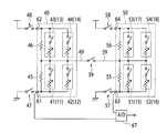
- FIG. 9 is a diagram showing a detection circuit diagram of the coordinate input device according to the present embodiment.
- the detection circuit includes a Y-direction coordinate detection unit 40 and an X-direction coordinate detection unit 50.
- the Y-direction first contact 41 (11) and the Y-direction second contact 42 (12) of the Y-direction first contact group 11, 12 and the first dummy resistor 45 are connected in parallel.
- One end 61 is connected to the ground level via the first switch 47, and the other is the Y-direction common potential line 49.
- the Y-direction third contact 43 (13) and the Y-direction fourth contact 44 (14) of the Y-direction second contact group 13, 14 are connected in parallel with the second dummy resistor 46, one of which is the Y-direction common potential.
- the other end 62 is connected to the power supply level via the second switch 48.
- the Y-direction first contact groups 11 and 12 and the Y-direction second contact group 13 are measured by measuring the potential of the Y-direction common potential line 49 with the first switch 47 and the second switch 48 turned on. , 14 can be detected.
- the resistance ratio between the corresponding dummy resistors 45 and 46 and the contact group in the on state can be detected.
- the X-direction first contact 51 (15) and the X-direction second contact 52 (16) of the X-direction first contact groups 15 and 16 and the third dummy resistor 55 are connected in parallel.
- One end 63 is connected to the ground level via the third switch 57, and the other is the X-direction common potential line 59.
- the X-direction third contact 53 (17) and the X-direction fourth contact 54 (18) of the X-direction second contact group 17, 18 are connected in parallel with the fourth dummy resistor 56, and one of them is the Y-direction common potential.
- the other end 64 is connected to the power supply level via the fourth switch 58.
- the X-direction first contact groups 15 and 16 and the X-direction second contact group 17 are measured by measuring the potential of the X-direction common potential line 59 with the third switch 57 and the fourth switch 58 turned on. , 18 can be detected.
- the resistance ratio between the corresponding dummy resistors 55 and 56 and the contact group in the on state can be detected.
- the dummy resistor 45,46,55,56 shall be 1-30 times the value of the ballast resistor R ON. This smaller and power consumption is increased, it becomes difficult to capture the transient change in resistance of up to stabilize the resistance R ON from a large and an insulating state. Furthermore, in order to obtain a practical output range, it is more preferably 2 to 6 times.
- inexpensive on - the conductive rubber for off for R ON is approximately 0.3 ⁇ 1 k [Omega, set around a 1 ⁇ 3.3k.
- the Y-direction common potential line 49 of the Y-direction coordinate detection unit 40 and the X-direction common potential line 59 of the X-direction coordinate detection unit 50 are connected via the fifth switch 39. As described above, when the Y direction coordinate detection unit 40 and the X direction coordinate detection unit 50 detect the XY coordinates independently, the fifth switch 39 is turned off.
- the fifth switch 39 is turned on to connect the Y-direction common potential line 49 of the Y-direction coordinate detection unit 40 and the X-direction common potential line 59 of the X-direction coordinate detection unit 50.
- the existing resistive touch panel interface can be diverted.
- the Y-direction coordinate detection unit 40 is, for example, a Y-side resistance film
- the X-direction coordinate detection unit 50 is an X-side resistance film
- the first switch 47 and the second switch 48 connected to the Y-direction coordinate detection unit 40, the X direction
- a so-called constant voltage driving system is used.
- input coordinates can be easily obtained.
- the Y-direction coordinate detection unit 40 is turned on and the X-direction coordinate detection unit 50 is turned off.
- the Y-direction common potential line 49 and the X-direction common potential line 59 have potentials related to the coordinates in the Y direction.
- the Y-direction coordinate detection unit 40 is turned off and the X-direction coordinate detection unit 50 is turned on.
- Y-direction common potential line 49 and the X-direction common potential line 59 potentials relating to coordinates in the X direction are obtained.
- the potentials of the Y-direction common potential line 49 and the X-direction common potential line 59 can be input to the interface of the resistive touch panel.
- the first switch 47 and the second switch 48 are turned on, the third switch 57 and the fourth switch 58 are turned off, and the Y direction coordinate detection unit 40 is turned on.
- the potential difference of the Y-side resistance film is measured at one end 61 or the other end 62 of the Y-side.
- the first switch 47 and the second switch 48 are turned off, the third switch 57 and the fourth switch 58 are turned on. Measure the potential difference. For example, such measurement can be performed by supplying the output of one end 61 of the Y direction coordinate detection unit 40 and one end 63 of the X direction coordinate detection unit 50 to the A / D converter 67.
- the fifth switch 39 can be omitted if it is not necessary to detect the start of the input operation on the coordinate input device side.
- the fifth switch 39 can also be constituted by the first central contact 19 and the central counter electrode 29 shown in FIG.
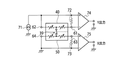
- FIG. 10 is a diagram showing a second embodiment of the coordinate input device.
- the fifth switch 39 connecting the Y direction coordinate detection unit 40 and the X direction coordinate detection unit 50 is turned on, and one end 61 of the Y direction coordinate detection unit 40 is fixed via the first detection resistor 72.
- the current source 71 is connected, and the other end 62 is directly connected to the constant current source 71.
- one end 63 of the X-direction coordinate detection unit 50 is connected to the ground level via the second detection resistor 73, and the other end 64 is directly connected to the ground level.
- the potential difference between the one end 61 and the other end 62 of the Y-direction coordinate detection unit 40 is detected as the Y output by detecting the potential difference between both ends of the first detection resistor 72 by the first differential amplifier 74. Further, the potential difference between the one end 63 and the other end 64 of the X direction coordinate detection unit 50 is detected as the X difference by detecting the potential difference between both ends of the second detection resistor 73 by the second differential amplifier 75.
- the second embodiment there is no need to switch between the Y-direction coordinate detection unit 40 and the X-direction coordinate detection unit 50. Therefore, since there is little noise associated with switching and the operating frequency is low, when a contact rubber with non-linear current / voltage characteristics is used, such as an inexpensive conductive rubber used for general on-off switches However, stable input coordinates can be obtained.
- Such a second embodiment also has a configuration equivalent to that obtained by diverting an existing interface for a resistive touch panel.
- the interface in this case corresponds to, for example, a constant current power source, first and second detection resistors 72 and 73, and first and second differential amplifiers 74 and 75.
- the Y-direction first contact groups 11 and 12 When the input operation is not performed, the Y-direction first contact groups 11 and 12, the Y-direction second contact groups 13 and 14, the X-direction first contact groups 15 and 16 and the X-direction second contact on the first substrate 10. Groups 17 and 18 are all off.
- the pressing member 32 shown in FIG. 7 When the pressing member 32 shown in FIG. 7 is pressed to apply a pressing force to the portion corresponding to the Y-direction first contact groups 11 and 12 in the negative region of the Y axis in FIG. 1, the second substrate 20 is displaced.
- the Y-direction first counter electrode 121 shown in FIG. 3 contacts the Y-direction first contact groups 11 and 12.
- the first electrode and the second electrode of the Y-direction first contact groups 11 and 12 are electrically connected, and the area where the Y-direction first counter electrode 121 contacts the Y-direction first contact groups 11 and 12 according to the pressing force.
- the resistance decreases and eventually becomes a constant stable resistance RON .
- comb-shaped contacts 11 to 18 having a diameter of 3 mm are arranged in a regular octagon on a circumference of 10 mm in the first substrate 10.
- a counter electrode having a curvature of 2.4 mm was formed of conductive silicon rubber 87C40P (manufactured by Shin-Etsu Polymer: rubber hardness 45 degrees).
- the annular pressing member 32 (see FIG. 7) was made of acrylic having a thickness of 0.9 mm. Ballast resistance R ON of the contacts 11-18 was 600 ⁇ when load 500 gf.
- the detection circuit shown in FIG. 9 is used, 3.3 k ⁇ is used as the first to fourth dummy resistors 45, 46, 55, 56, the fifth switch 39 is turned on, and the Y-direction coordinate detection unit 40 is common in the Y direction.
- the potential line 49 and the X-direction common potential line 59 of the X-direction coordinate detection unit 50 are connected.
- the circuit configuration shown in FIG. 10 was applied, the first detection resistor 72 and the second detection resistor 73 were each set to 20 ⁇ , and the 1 mA constant current source 71 was used.
- a potential difference between both ends of the first detection resistor 72 and the second detection resistor 73 is detected by a first differential amplifier 74 and a second differential amplifier 75 having an internal resistance of 1 k ⁇ and a differential gain of 200 times, and Y output and X output, respectively. It was.
- the present invention can be used for coordinate input in various electronic devices such as portable terminals.
Landscapes
- Engineering & Computer Science (AREA)
- General Engineering & Computer Science (AREA)
- Theoretical Computer Science (AREA)
- Human Computer Interaction (AREA)
- Physics & Mathematics (AREA)
- General Physics & Mathematics (AREA)
- Position Input By Displaying (AREA)
Abstract
既存のインターフェイスを使用し、安価な導電ゴムの接点を使用し、かつ、四角形の座標出力の座標入力装置を提供する。Y方向第1接点群(11,12)及びY方向第2接点群(13,14)は、それぞれ、Y軸を挟んで対向する2個の接点を有し、X方向第1接点群(15,16)及びX方向第2接点群(17,18)は、それぞれ、X軸を挟んで対向する2個の接点を有し、Y方向第1接点群(11,12)、Y方向第2接点群(13,14)、X方向第1接点群(15,16)及びX方向第2接点群(17,18)の各接点は、それぞれ、第1電極及び第2電極を有し、Y方向第1対向電極(121)、Y方向第2対向電極(122)、X方向第1対向電極(123)及びX方向第2対向電極(124)は、第1基板(10)に接触すると、それぞれ第1電極及び第2電極を電気的に導通し、かつ、第1基板に接触する面積を可変できる弾性体からなる。
Description
本発明は、携帯端末などに使用される座標入力装置に関する。
従来、電話や各種のゲーム機などの携帯端末における座標入力装置として、東西南北方向とその間に複数の接点を設け、その接点のオン-オフで、入力ベクトルを検出するいわゆる多方向キー(特許文献1)が知られている。この方法は、検出が簡便である反面、ベクトルの方向の検出精度が接点数に依存し、また、大きさについては検出が困難などの問題があった。
これらオン-オフ接点に代えて、固定接点に感圧導電ゴムからなる可動接点を組み合わせ、アナログ的に入力ベクトルを検出する座標入力装置(特許文献2、特許文献3)が知られている。これらの方法は、高価な感圧導電ゴムを使用しなければならず、また、個々の接点の導通抵抗を求めた上で、基板上の接点の座標データから入力ベクトルを計算しなければならない。
また、2つの感圧抵抗素子の抵抗比を測定する検出方法(特許文献4)も提案されているが、やはり専用の検出回路を用意しなければならず、かつ、キーパッドなど他のオン-オフタイプの入力装置のほかスクリーン印刷で、感圧抵抗素子を形成しなければならず、この荷重-抵抗特性の管理など手間がかかる。
また、何れの方法でも、得られる座標は、何らかの補正を行なわない限り、接点の配列と同様の円形のものであり、特に東西南北に各1個の接点しかない場合は東西南北を頂点とするひし形となるため、長方形の表示画面に一致させるためには何らかの補正が必要であった。
一方、LCDやCRTなどが表示画面上においてタッチした位置を検出するタッチパネルが提供されている。タッチパネルとしては抵抗膜方式のものが多く利用され、この抵抗膜方式のためのインターフェイスデバイスが流通している。
本発明は、既存のインターフェイスを使用することができ、安価な導電ゴムの接点を使用し、かつ、接点の構成によっては携帯機器などに使用される表示画面と同様の四角形の座標出力を容易に得ることができる座標入力装置を提供することを目的とする。
上述の課題を解決するために、本発明の一態様は、主面にXY直交座標系が設定され、原点を挟んでY方向に対向して配置されたY方向第1接点群及びY方向第2接点群と、原点を挟んでX方向に対向して配置されたX方向第1接点群及びX方向第2接点群とを有し、前記Y方向第1接点群及び前記Y方向第2接点群が、それぞれY軸を挟んで対向する2個の接点を有し、前記X方向第1接点群及び前記X方向第2接点群が、それぞれX軸を挟んで対向する2個の接点を有し、前記Y方向第1接点群及び前記Y方向第2接点群並びに前記X方向第1接点群及び前記X方向第2接点群の各接点が、それぞれ第1電極及び第2電極を有する第1基板と、前記第1基板に対向する主面に、前記Y方向第1接点群及び前記Y方向第2接点群にそれぞれ対向して配置されたY方向第1対向電極及びY方向第2対向電極と、前記X方向第1接点群及び前記X方向第2接点群にそれぞれ対向して配置されたX方向第1対向電極及びX方向第2対向電極とを有する、前記第1基板に対して変位可能な第2基板とを有し、前記Y方向第1対向電極、前記Y方向第2対向電極、前記X方向第1対向電極及び前記X方向第2対向電極は、前記第1基板に接触すると、それぞれ第1電極及び第2電極を電気的に導通し、かつ前記第1基板に接触する面積を可変できる弾性体からなる。
本発明によると、既存のインターフェイスを使用することができ、安価な導電ゴムの接点を使用し、かつ、接点の構成によっては携帯機器などに使用される表示画面と同様の四角形の座標出力を容易に得ることができる。
次に、図面を参照して、本発明の実施の形態を説明する。以下の図面の記載において、同一又は類似の部分には同一又は類似の符号を付している。ただし、図面は模式的なものであり、各構成部材の比率等は現実のものとは異なることに留意すべきである。したがって、具体的な寸法は以下の説明を参酌して判断すべきものである。又、図面相互間においても互いの寸法の関係や比率が異なる部分が含まれていることはもちろんである。
又、以下に示す実施の形態は、この発明の技術的思想を具体化するための装置や方法を例示するものであって、この発明の実施の形態は、構成部材の材質、形状、構造、配置等を下記のものに特定するものでない。この発明の実施の形態は、特許請求の範囲において、種々の変更を加えることができる。
[第1の実施の形態]
図1は、第1の実施の形態の座標入力装置の接点配置の一例を示す図である。
図1は、第1の実施の形態の座標入力装置の接点配置の一例を示す図である。
座標入力装置においては、平坦な絶縁性の第1基板10の主面内にXY直交座標系が設定され、Y方向に原点Oを挟んで対向するY方向第1接点群11,12及びY方向第2接点群13,14が形成されている。また、X方向に原点Oを挟んで対向するX方向第1接点群15,16及びX方向第2接点群17,18が形成されている。
Y方向第1接点群11,12は、Y軸を挟んで対向するY方向第1接点11及びY方向第2接点12から構成され、Y方向第2接点群13,14は、Y軸を挟んで対向するY方向第3接点13及びY方向第4接点14から構成されている。X方向第1接点群15,16は、X軸を挟んで対向するX方向第1接点15及びX方向第2接点16から構成され、X方向第2接点群17,18は、X軸を挟んで対向するX方向第3接点17及びX方向第4接点18から構成されている。
図2は、Y方向第1接点11を示す図である。
Y方向第1接点11は、櫛歯形状に形成され、互いに嵌め込まれるように配置された第1電極11a及び第2電極11bから構成されている。他の接点12~18も、同様な形状に構成されている。このような櫛歯形状の電極は、後述する対向電極の面積を正確に検出することにより、良好な感圧特性を有する。
なお、本実施の形態の接点11~18は、櫛歯形状に限られず、平行に伸びる電極など他の形状として構成することもできる。
図1に戻り、Y方向第1接点群11,12のY方向第1接点11及びY方向第2接点12と、Y方向第2接点群13,14のY方向第3接点13及びY方向第4接点14は、矩形の如き四角形状1を構成している。これらのY方向第1接点群11,12及びY方向第2接点群13,14は、Y方向押圧検出手段を構成している。
同様に、X方向第1接点群15,16のX方向第1接点15及びX方向第2接点16と、X方向第2接点群17,18のX方向第3接点17及びX方向第4接点18も、矩形の如き四角形状2を構成している。これらX方向第1接点群15,16及びX方向第2接点群17,18は、X方向押圧検出手段を構成している。
また、Y方向第1~第4接点11~14及びX方向第1~第4接点15~18は、原点Oから等距離の円周3上に位置している。なお、Y方向第1~第4接点11~14及びX方向第1~第4接点15~18は、円周3上に限らず、楕円周上に位置してもよい。
図3は、第1基板に対向する第2基板に設けられた対向電極の配置を示す図である。
第2基板20は、第1基板10に対向して変位可能に所定距離をおいて配置される。第2基板20の平坦な絶縁性の主面上には、第1基板10のY方向第1接点群11,12のY方向第1接点11及びY方向第2接点12に対向する第1対向電極21及び第2対向電極22を有するY方向第1対向電極121が設けられ、Y方向第2接点群13,14のY方向第3接点13及びY方向第4接点14に対向する第3対向電極23及び第4対向電極24を有するY方向第2対向電極122が設けられている。また、X方向第1接点群15,16のX方向第1接点15及びX方向第2接点16に対向する第5対向電極25及び第6対向電極26を有するX方向第1対向電極123が設けられ、X方向第2接点群17,18のX方向第3接点17及びX方向第4接点18に対向する第7対向電極27及び第8対向電極28を有するX方向第2対向電極124が設けられている。
これらの対向電極121~124を構成する第1~第8対向電極21~28は、例えばシリコンゴムにカーボン系、あるいは銀系、あるいはその他の導電粒子を配合した所謂導電ゴムで略球面状に成型されている。この導電ゴムは、感圧導電グレードと言われるものの他、一般のオン-オフスイッチに使用される安価な導電ゴムを使用することができる。
図4は、第1基板に対向する第2基板に設けられた対向電極の配置の他の態様を示す図である。
本実施の形態は、図3に示したような構成に限られず、Y方向第1対向電極121、Y方向第2対向電極122、X方向第1対向電極123及びX方向第2対向電極124を単一の電極として構成することもできる。
この態様では、第2基板20の主面上には、第1基板10のY方向第1接点群11,12に対向するY方向第1対向電極121が設けられ、Y方向第2接点群13,14に対向するY方向第2対向電極122が設けられている。また、X方向第1接点群15,16に対向するX方向第1対向電極123が設けられ、X方向第2接点群17,18に対向するX方向第2対向電極124が設けられている。
図5は、導電ゴムの押圧荷重に対する抵抗特性を示す図である。
図中の曲線aは、感圧導電グレードの導電ゴムの特性を示す。このような導電ゴムは、押圧荷重が増加するにつれて抵抗が減少し、一定の安定抵抗RONに漸近的に近づく。図中の曲線bは、オン-オフスイッチに使用される導電ゴムの特性を示す。このような導電ゴムは、押圧荷重が増加すると急峻に抵抗が減少してある安定抵抗RONとなる。
なお、ゴム硬度は、JIS K6253タイプAに規定された35~80度が好ましく、操作感からは40度以上、耐久性からは75度以下、トータルのバランスから45~70度の範囲に設定することがより好ましい。
図6は、接点と対向電極の関係を示す図である。
第2基板20は、第1基板10に対して変位可能に所定距離おいて支持されている。第2基板20において、Y方向第1対向電極121の第1対向電極21は、第1基板10に形成された第1接点群11,12を構成するY方向第1接点11の第1電極11a及び第2電極11bに対向するように形成されている。
第2基板20は、押圧時には、第1対向電極21が押圧荷重に応じてY方向第1接点11に対して押し付けられ、第1電極11a及び第2電極11b間を導通する。導電ゴムからなる第1対向電極21がY方向第1接点11に接触する面積は、ゴムの弾性力により押圧力に応じて増加する。
したがって、第1電極11a及び第2電極11b間は、押圧力が所定値に達すると導通され、その後は押圧力に応じて抵抗値が減少するか、または所定値の安定抵抗RONに達するとその値で留まる。
なお、ここではY方向第1接点群11,12のうちY方向第1接点11について第1対向電極21との関係を示したが、Y方向第1接点群11,12のY方向第2接点12、Y方向第2接点群13,14、X方向第1接点群15,16及びX方向第2接点群17,18についても、対応する対向電極22~28と同様の関係を有する。
図7は、本実施の形態の座標入力装置の断面図である。
この図は、図1に示した第1基板10を直線I-Iで、図3に示した第2基板20を直線II-IIで切断した断面に相当するものである。
図7Aは、押圧操作をしていない状態での座標入力装置の断面図である。第2基板20は、第1基板10に対して変位可能なように、ドーム状の弾性支持部材31によって第1基板10に対して所定距離をおいて支持されている。
第1基板10には、Y方向第1接点群11,12のY方向第1接点11の第1電極11a及び第2電極11b、Y方向第2接点群13,14のY方向第4接点14の第1電極14a及び第2電極14bが形成されている。第2基板20には、Y方向第1接点11に対向して対向電極21、Y方向第4接点14に対向して第4対向電極24が、それぞれ形成されている。
弾性支持部材31においては、第2基板20を配置する反対側の面に、第2基板20に対して押圧力を加えるために指などで操作可能な押圧部材32が設けられている。
このように押圧されていない状態では、対向電極は対向する第1及び第2電極から離間された状態で保持されるか、少なくとも僅少な押圧力で第1及び第2電極に接触するため、第1及び第2電極間は絶縁されているかまたは十分に高い抵抗値を示す。
図7Bは、押圧操作をした状態での座標入力装置の断面図である。
押圧部材32に指100などにより押圧力が加えられると、弾性支持部材31は、弾性的に変形し、必要に応じて座屈することでクリック感を生じさせる。
ここでは、Y方向第1接点群11,12のY方向第1接点11の第1電極11a及び第2電極11bが第1対向電極21に接触し、第1電極11aと第2電極12a間の抵抗は押圧力の増加に従い急速に減少し、やがて一定の安定抵抗RONとなる。
なお、この図3においては、Y方向第1接点群11,12のY方向第1接点11及びY方向第2接点群13,14のY方向第4接点14について例示したが、このことは他の接点群に対しても同様である。
図8は、他の態様の座標入力装置の断面図である。
他の態様においては、第1基板10及び第2基板20の中央部に、それぞれ第1中央接点19(第3の接点)及び中央対向電極29が形成されている。第1中央接点19は、第1電極19a及び第2電極19bから構成されている。このような中央部に設けられた接点及び対向電極19,29は、座標入力の操作開始を検出するために設けることができる。
なお、このような入力操作の検出のための接点及び対向電極は、第1基板10及び第2基板20の中央部に限られず、外周部に設けることもできる。
図9は、本実施の形態の座標入力装置の検出回路図を示す図である。
この検出回路は、Y方向座標検出部40及びX方向座標検出部50から構成されている。
Y方向座標検出部40においては、Y方向第1接点群11,12のY方向第1接点41(11)及びY方向第2接点42(12)と第1ダミー抵抗45とが並列接続され、その一端61が第1スイッチ47を介して接地レベルに接続され、他方がY方向共通電位線49とされている。
ここで、この回路図においては、Y方向第1接点群11,12のY方向第1接点11及びY方向第2接点12をスイッチと可変抵抗が直列接続された等価回路41,42で示し、対応関係を明らかにするために符号41(11)、42(12)で示すことにする。以下でも同様とする。
また、Y方向第2接点群13,14のY方向第3接点43(13)及びY方向第4接点44(14)が第2ダミー抵抗46とが並列接続され、その一方がY方向共通電位線49とされ、その他端62が第2スイッチ48を介して電源レベルに接続されている。
ここで、第1スイッチ47及び第2スイッチ48をオンとした状態で、Y方向共通電位線49の電位を測定することで、Y方向第1接点群11,12とY方向第2接点群13,14のオン抵抗比を検出することができる。または、いずれか一方の接点群がオフ状態では、対応するダミー抵抗45,46とオン状態の接点群の抵抗比を検出することができる。
X方向座標検出部50においては、X方向第1接点群15,16のX方向第1接点51(15)及びX方向第2接点52(16)と第3ダミー抵抗55とが並列接続され、その一端63が第3スイッチ57を介して接地レベルに接続され、他方がX方向共通電位線59とされている。
また、X方向第2接点群17,18のX方向第3接点53(17)及びX方向第4接点54(18)が第4ダミー抵抗56とが並列接続され、その一方がY方向共通電位線59とされ、他端64が第4スイッチ58を介して電源レベルに接続されている。
ここで、第3スイッチ57及び第4スイッチ58をオンとした状態で、X方向共通電位線59の電位を測定することで、X方向第1接点群15,16とX方向第2接点群17,18のオン抵抗比を検出することができる。または、いずれか一方の接点群がオフ状態では、対応するダミー抵抗55,56とオン状態の接点群の抵抗比を検出することができる。
なお、ダミー抵抗45,46,55,56は、安定抵抗RONの値の1~30倍とする。これより小さいと消費電力が増大し、大きいと絶縁状態から安定抵抗RONに至るまでの過渡的な抵抗変化を捉えることが難しくなる。さらに、実用上、適切な出力レンジを得るために、より好ましくは2~6倍である。通常、安価なオン-オフ用の導電ゴムではRONは概ね0.3~1kΩであるため、1~3.3kΩを中心に設定する。
これらY方向座標検出部40のY方向共通電位線49とX方向座標検出部50のX方向共通電位線59は、第5スイッチ39を介して接続されている。上述のように、Y方向座標検出部40とX方向座標検出部50において、XY座標を独立に検出する場合には、この第5スイッチ39はオフとされている。
本実施の形態の座標入力装置は、第5スイッチ39をオンとしてY方向座標検出部40のY方向共通電位線49とX方向座標検出部50のX方向共通電位線59を接続することにより、既存の抵抗膜式タッチパネルのインターフェイスを転用することができる。
すなわち、Y方向座標検出部40を例えばY側抵抗膜とし、X方向座標検出部50をX側抵抗膜とし、Y方向座標検出部40に接続する第1スイッチ47及び第2スイッチ48、X方向座標検出部50の接続する第3スイッチ57及び第4スイッチ58の組み合わせを交互にオン-オフし、Y方向座標検出部40とX方向座標検出部50を切り替えることにより、所謂定電圧駆動方式の抵抗膜式タッチパネルと同様に簡便に入力座標を得ることが可能になる。
具体的に、第1スイッチ47及び第2スイッチ48をオンとし、第3スイッチ57及び第4スイッチ58をオフとすることにより、Y方向座標検出部40がオン、X方向座標検出部50がオフとなり、Y方向共通電位線49及びX方向共通電位線59には、Y方向の座標に関する電位が得られる。一方、第1スイッチ47及び第2スイッチ48をオフとし、第3スイッチ57及び第4スイッチ58をオンとすることにより、Y方向座標検出部40がオフ、X方向座標検出部50がオンとなり、Y方向共通電位線49及びX方向共通電位線59には、X方向の座標に関する電位が得られる。これらY方向共通電位線49及びX方向共通電位線59の電位を抵抗膜式タッチパネルのインターフェイスへの入力とすることができる。
既存の抵抗膜式タッチパネルインターフェースを転用する場合は、Y方向の測定では、第1スイッチ47及び第2スイッチ48をオン、第3スイッチ57及び第4スイッチ58をオフとし、Y方向座標検出部40の一端61または他端62でY側抵抗膜の電位差を測定する。X方向の測定では、第1スイッチ47及び第2スイッチ48をオフ、第3スイッチ57及び第4スイッチ58をオンとし、X方向座標検出部50の一端63または他端64でX側抵抗膜の電位差を測定する。例えば、このような測定は、Y方向座標検出部40の一端61とX方向座標検出部50の一端63の出力をA/Dコンバータ67に供給することで行うことができる。
なお、第5のスイッチ39は、入力操作の開始を座標入力装置側で検出する必要がなければ省略することができる。この第5のスイッチ39は、図8に示した第1中央接点19及び中央対向電極29で構成することもできる。
[第2の実施の形態]
図10は、座標入力装置の第2の実施の形態を示す図である。
図10は、座標入力装置の第2の実施の形態を示す図である。
第2の実施の形態では、Y方向座標検出部40とX方向座標検出部50を結ぶ第5スイッチ39をオンとし、Y方向座標検出部40の一端61を第1検出抵抗72を介して定電流源71を接続し、他端62を直接に定電流源71に接続する。また、X方向座標検出部50の一端63を第2検出抵抗73を介して接地レベルに接続し、他端64は直接に接地レベルに接続する。
そして、Y方向座標検出部40の一端61と他端62の間の電位差を第1検出抵抗72の両端の電位差を第1差動アンプ74により検出することでY出力とする。また、X方向座標検出部50の一端63と他端64の間の電位差を第2検出抵抗73の両端の電位差を第2差動アンプ75により検出することでX出力とする。
この第2の実施の形態によると、Y方向座標検出部40とX方向座標検出部50を切り替える必要がない。したがって、切り替えに伴うノイズが少なく、かつ動作周波数が低いため、導電ゴムとして般のオン-オフスイッチに使用される安価な導電ゴムのように接点の電流・電圧特性が非線形のものを使用した場合でも、安定した入力座標を得ることが可能である。
このような第2の実施の形態も、既存の抵抗膜式タッチパネル用のインターフェイスを転用したものと同等の構成である。この場合のインターフェイスには、例えば定電流電源、第1及び第2検出抵抗72,73及び第1及び第2差動アンプ74,75が相当する。
次に、本実施の形態の座標入力装置の動作について説明する。
入力操作を行なっていない状態では、第1基板10上のY方向第1接点群11,12、Y方向第2接点群13,14、X方向第1接点群15,16及びX方向第2接点群17,18は、すべてオフの状態である。
図7に示した押圧部材32を押圧することにより、図1のY軸の負の領域のY方向第1接点群11,12に相当する部分に押圧力を加えると、第2基板20が変位し、図3に示したY方向第1対向電極121がY方向第1接点群11,12に接触する。これによって、Y方向第1接点群11,12の第1電極及び第2電極がそれぞれ導通し、押圧力にしたがってY方向第1対向電極121がY方向第1接点群11,12に接触する面積が増加するにつれて抵抗が減少し、やがて一定の安定抵抗RONとなる。
この状態で、押圧位置を原点Oに関して時計周り方向に移動すると、Y方向第1接点群11,12のY方向第2接点12の抵抗が上昇し、やがてオフ状態となり、Y方向第2接点群13,14のY方向第4接点14がY方向第2対向電極122に接触し抵抗が減少する。さらに押圧位置を時計回り方向に移動するとやがてY方向第1接点群11,12のY方向第1接点11がオフになり、Y方向第2接点群13,14のY方向第3接点13がY方向第2対向電極122に接触し、Y方向第2接点群13,14のY方向第3接点13及びY方向第4接点14が同時にオンの状態となる。
なお、ここではY方向第1接点群11,12及びY方向第2接点群13,14についての動作を説明したが、X方向第2接点群15,16及びX方向第2接点群17,18についての動作も同様である。
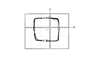
この座標入力装置の出力電圧をXY面内でプロットすると、各接点11~18の抵抗がRONになるような大きな力で環状の押圧部材32を押圧し、図1の原点Oの周囲を円を描くようになぞるような操作を行なった場合、略四角形の図形が描かれた。一方、各接点11~18の抵抗がRONに至らない小さな力で同様に押圧部材32をなぞる操作を行った場合、電圧は略円形の図形が描かれた。
図11に示すように、第1基板10において直径10mmの円周上に直径3mmの櫛歯状接点11~18を正八角形に配置した。第1基板10に対向する第2基板20上に、導電性のシリコンゴム87C40P(信越ポリマー製:ゴム硬度45度)で曲率2.4mmの対向電極を形成した。環状の押圧部材32(図7参照)は、厚み0.9mmのアクリル製とした。接点11~18の安定抵抗RONは、荷重500gfのとき600Ωであった。
図9に示した検出回路を使用し、第1~第4ダミー抵抗45,46,55,56として3.3kΩを使用し、第5スイッチ39をオンとしてY方向座標検出部40のY方向共通電位線49とX方向座標検出部50のX方向共通電位線59を接続した。
そして、図10に示した回路構成を適用し、第1検出抵抗72及び第2検出抵抗73をそれぞれ20Ωとし、1mAの定電流源71を用いた。第1検出抵抗72及び第2検出抵抗73の両端の電位差を、内部抵抗1kΩ、差動利得200倍の第1差動アンプ74及び第2差動アンプ75で検出し、それぞれY出力及びX出力とした。
環状の押圧部材32の表面を親指で強く押しながら、円を描くようになぞり、インターフェイスの出力をXY面に表示した。その結果、図12に示すような略四角形状の図形が観察された。
一方、環状の押圧部材32の表面を小指で弱く押しながら、円を描くようになぞり、インターフェイスの出力をXY面に表示した。その結果、図13に示すような略円周状の図形が観察された。
[第3の実施の形態]
次に、櫛歯状接点を正四角形に配置し、その他は同様に座標入力装置を構成した入力を行なった。
次に、櫛歯状接点を正四角形に配置し、その他は同様に座標入力装置を構成した入力を行なった。
環状の押圧部材32の表面を親指で強く押しながら、円を描くようになぞり、インターフェイスの出力をXY面に表示した。その結果、図14に示すようなXY方向とは各辺の方向が異なるひし形状の図形が描かれた。また、XY方向の接点の切り替えに際しても波形に乱れが生じたことが観察されたが、座標データを得ることができた。
[その他の実施の形態]
上記のように、本発明は実施の形態によって記載したが、この開示の一部をなす論述および図面は例示的なものであり、この発明を限定するものであると理解すべきではない。この開示から当業者には様々な代替実施の形態、実施例および運用技術が明らかとなろう。
上記のように、本発明は実施の形態によって記載したが、この開示の一部をなす論述および図面は例示的なものであり、この発明を限定するものであると理解すべきではない。この開示から当業者には様々な代替実施の形態、実施例および運用技術が明らかとなろう。
このように、本発明はここでは記載していない様々な実施の形態などを含む。
本発明は、携帯端末などさまざまな電子機器における座標入力に使用することができる。
10 第1基板
11,12 Y方向第1接点群
13,14 Y方向第2接点群
15.16 X方向第1接点群
17,18 X方向第2接点群
20 第2基板
21~28 第1~第8対向電極
121 Y方向第1対向電極
122 Y方向第2対向電極
123 X方向第1対向電極
124 X方向第2対向電極
11,12 Y方向第1接点群
13,14 Y方向第2接点群
15.16 X方向第1接点群
17,18 X方向第2接点群
20 第2基板
21~28 第1~第8対向電極
121 Y方向第1対向電極
122 Y方向第2対向電極
123 X方向第1対向電極
124 X方向第2対向電極
Claims (12)
- 主面にXY直交座標系が設定され、原点を挟んでY方向に対向して配置されたY方向第1接点群及びY方向第2接点群と、原点を挟んでX方向に対向して配置されたX方向第1接点群及びX方向第2接点群とを有し、前記Y方向第1接点群及び前記Y方向第2接点群が、それぞれY軸を挟んで対向する2個の接点を有し、前記X方向第1接点群及び前記X方向第2接点群が、それぞれX軸を挟んで対向する2個の接点を有し、前記Y方向第1接点群及び前記Y方向第2接点群並びに前記X方向第1接点群及び前記X方向第2接点群の各接点が、それぞれ第1電極及び第2電極を有する第1基板と、
前記第1基板に対向する主面に、前記Y方向第1接点群及び前記Y方向第2接点群にそれぞれ対向して配置されたY方向第1対向電極及びY方向第2対向電極と、前記X方向第1接点群及び前記X方向第2接点群にそれぞれ対向して配置されたX方向第1対向電極及びX方向第2対向電極とを有する、前記第1基板に対して変位可能な第2基板とを有し、
前記Y方向第1対向電極、前記Y方向第2対向電極、前記X方向第1対向電極及び前記X方向第2対向電極は、前記第1基板に接触すると、それぞれ第1電極及び第2電極を電気的に導通し、かつ前記第1基板に接触する面積を可変できる弾性体からなることを特徴とする座標入力装置。 - 前記Y方向第1対向電極及び前記Y方向第2対向電極は、それぞれY軸を挟んで対向する2個の対向電極を有し、前記X方向第1対向電極及び前記X方向第2対向電極は、それぞれX軸を挟んで対向する2個の対向電極を有することを特徴とする請求項1記載の座標入力装置。
- 前記Y方向第1接点群、前記Y方向第2接点群、前記X方向第1接点群及び前記X方向第2接点群が含む2個の接点は、それぞれ並列に接続されることを特徴とする請求項1又は2記載の座標入力装置。
- 前記Y方向第1接点群、前記Y方向第2接点群、前記X方向第1接点群及び前記X方向第2接点群に並列に抵抗を接続したことを特徴とする請求項3記載の座標入力装置。
- 前記Y方向第1接点群及び前記Y方向第2接点群は直列に接続され、前記X方向第1接点群及び前記X方向第2接点群は直列に接続されることを特徴とする請求項4記載の座標入力装置。
- 前記Y方向第1接点群、前記Y方向第2接点群、前記X方向第1接点群及び前記X方向第2接点群のほかに第3の接点または接点群を有することを特徴とする請求項1乃至5のいずれかに記載の座標入力装置。
- 前記Y方向第1対向電極、前記Y方向第2対向電極、前記X方向第1対向電極及び前記X方向第2対向電極は、導電ゴムからなることを特徴とする請求項1乃至6のいずれかに記載の座標入力装置。
- 前記Y方向第1接点群及び前記Y方向第2接点群の各接点は、四角形を構成することを特徴とする請求項1乃至7のいずれかに記載の座標入力装置。
- 前記X方向第1接点群及び前記X方向第2接点群の各接点は、四角形を構成することを特徴とする請求項1乃至8のいずれかに記載の座標入力装置。
- 前記Y方向第1接点群、前記Y方向第2接点群、前記X方向第1接点群及び前記X方向第2接点群の各接点は、円周又は楕円周上にあることを特徴とする請求項1乃至9のいずれかに記載の座標入力装置。
- 前記第1基板に対して前記第2基板を変位可能に支持する弾性支持部材をさらに有することを特徴とする請求項1乃至10のいずれかに記載の座標入力装置。
- 前記第1電極及び前記第2電極は、櫛歯状であることを特徴とする請求項1乃至11のいずれかに記載の座標入力装置。
Applications Claiming Priority (2)
| Application Number | Priority Date | Filing Date | Title |
|---|---|---|---|
| JP2009241711A JP2011090402A (ja) | 2009-10-20 | 2009-10-20 | 座標入力装置 |
| JP2009-241711 | 2009-10-20 |
Publications (1)
| Publication Number | Publication Date |
|---|---|
| WO2011049083A1 true WO2011049083A1 (ja) | 2011-04-28 |
Family
ID=43900307
Family Applications (1)
| Application Number | Title | Priority Date | Filing Date |
|---|---|---|---|
| PCT/JP2010/068380 Ceased WO2011049083A1 (ja) | 2009-10-20 | 2010-10-19 | 座標入力装置 |
Country Status (2)
| Country | Link |
|---|---|
| JP (1) | JP2011090402A (ja) |
| WO (1) | WO2011049083A1 (ja) |
Citations (1)
| Publication number | Priority date | Publication date | Assignee | Title |
|---|---|---|---|---|
| JPH11126126A (ja) * | 1997-10-23 | 1999-05-11 | Fujitsu Ltd | 携帯電話機用スクロールスイッチ装置 |
-
2009
- 2009-10-20 JP JP2009241711A patent/JP2011090402A/ja active Pending
-
2010
- 2010-10-19 WO PCT/JP2010/068380 patent/WO2011049083A1/ja not_active Ceased
Patent Citations (1)
| Publication number | Priority date | Publication date | Assignee | Title |
|---|---|---|---|---|
| JPH11126126A (ja) * | 1997-10-23 | 1999-05-11 | Fujitsu Ltd | 携帯電話機用スクロールスイッチ装置 |
Also Published As
| Publication number | Publication date |
|---|---|
| JP2011090402A (ja) | 2011-05-06 |
Similar Documents
| Publication | Publication Date | Title |
|---|---|---|
| US10042455B2 (en) | Detecting sensor having position detection and pressing force detection electrodes | |
| US7064561B2 (en) | Resistance type sensor | |
| EP2407864A1 (en) | Pressure sensitive touch control device | |
| JP4260406B2 (ja) | 押圧方向検出センサ及びこれを用いた入力装置 | |
| JP3539794B2 (ja) | タッチパネル及びディジタイザ機能を兼ね備えた情報入力装置及びその駆動方法 | |
| CN100381989C (zh) | 位置检测设备及包括其的数据输入设备 | |
| US20120086668A1 (en) | Integrated touch control device | |
| KR101004941B1 (ko) | 촉각 센서 | |
| JP6493608B1 (ja) | タッチパネル | |
| JP5266186B2 (ja) | 座標入力装置 | |
| WO2011049117A1 (ja) | 座標入力装置 | |
| JP4303167B2 (ja) | 入力装置 | |
| WO2011049083A1 (ja) | 座標入力装置 | |
| WO2006002661A1 (en) | Keypad signal input apparatus | |
| JP2011076341A (ja) | タッチパネル測定治具および測定方法 | |
| JP4508886B2 (ja) | 抵抗膜方式タッチパネル | |
| KR101370811B1 (ko) | 멤브레인 스위치시트와 이를 포함하는 멤브레인 스위치 키보드 | |
| JP2006521606A (ja) | 内蔵された信号検出要素を有するキーボードの連続操作可能なキー及び信号を処理する方法 | |
| JP2008146679A (ja) | 入力装置及びそれを備えた電子機器 | |
| KR101876128B1 (ko) | 벡터 포인팅 디바이스 및 그의 벡터 포인팅 검출 방법 | |
| JP3406078B2 (ja) | 座標指示器および位置入力装置 | |
| JPH0659798A (ja) | 座標入力装置 | |
| JPS58103077A (ja) | 座標入力装置 | |
| JP2011096488A (ja) | 抵抗シート、感圧スイッチおよびそれを用いた入力装置 | |
| JPH06202790A (ja) | 座標入力装置 |
Legal Events
| Date | Code | Title | Description |
|---|---|---|---|
| 121 | Ep: the epo has been informed by wipo that ep was designated in this application |
Ref document number: 10824932 Country of ref document: EP Kind code of ref document: A1 |
|
| 122 | Ep: pct application non-entry in european phase |
Ref document number: 10824932 Country of ref document: EP Kind code of ref document: A1 |