WO2011042964A1 - 電子放出素子の製造方法 - Google Patents
電子放出素子の製造方法 Download PDFInfo
- Publication number
- WO2011042964A1 WO2011042964A1 PCT/JP2009/067498 JP2009067498W WO2011042964A1 WO 2011042964 A1 WO2011042964 A1 WO 2011042964A1 JP 2009067498 W JP2009067498 W JP 2009067498W WO 2011042964 A1 WO2011042964 A1 WO 2011042964A1
- Authority
- WO
- WIPO (PCT)
- Prior art keywords
- electron
- conductive film
- cathode
- insulating layer
- emitting device
- Prior art date
- Legal status (The legal status is an assumption and is not a legal conclusion. Google has not performed a legal analysis and makes no representation as to the accuracy of the status listed.)
- Ceased
Links
Images




Classifications
-
- H—ELECTRICITY
- H01—ELECTRIC ELEMENTS
- H01J—ELECTRIC DISCHARGE TUBES OR DISCHARGE LAMPS
- H01J9/00—Apparatus or processes specially adapted for the manufacture, installation, removal, maintenance of electric discharge tubes, discharge lamps, or parts thereof; Recovery of material from discharge tubes or lamps
- H01J9/02—Manufacture of electrodes or electrode systems
- H01J9/022—Manufacture of electrodes or electrode systems of cold cathodes
- H01J9/027—Manufacture of electrodes or electrode systems of cold cathodes of thin film cathodes
-
- H—ELECTRICITY
- H01—ELECTRIC ELEMENTS
- H01J—ELECTRIC DISCHARGE TUBES OR DISCHARGE LAMPS
- H01J1/00—Details of electrodes, of magnetic control means, of screens, or of the mounting or spacing thereof, common to two or more basic types of discharge tubes or lamps
- H01J1/02—Main electrodes
- H01J1/30—Cold cathodes, e.g. field-emissive cathode
- H01J1/316—Cold cathodes, e.g. field-emissive cathode having an electric field parallel to the surface, e.g. thin film cathodes
-
- H—ELECTRICITY
- H01—ELECTRIC ELEMENTS
- H01J—ELECTRIC DISCHARGE TUBES OR DISCHARGE LAMPS
- H01J31/00—Cathode ray tubes; Electron beam tubes
- H01J31/08—Cathode ray tubes; Electron beam tubes having a screen on or from which an image or pattern is formed, picked up, converted, or stored
- H01J31/10—Image or pattern display tubes, i.e. having electrical input and optical output; Flying-spot tubes for scanning purposes
- H01J31/12—Image or pattern display tubes, i.e. having electrical input and optical output; Flying-spot tubes for scanning purposes with luminescent screen
- H01J31/123—Flat display tubes
- H01J31/125—Flat display tubes provided with control means permitting the electron beam to reach selected parts of the screen, e.g. digital selection
- H01J31/127—Flat display tubes provided with control means permitting the electron beam to reach selected parts of the screen, e.g. digital selection using large area or array sources, i.e. essentially a source for each pixel group
Definitions
- the present invention relates to an electron-emitting device used for a display or the like.
- Patent Document 1 discloses a field emission type electron-emitting device having a fine protrusion portion where an electric field concentrates.
- Patent Document 2 discloses an electron-emitting device in which irregularities are provided on the surface of a conductive film.
- Patent Document 3 discloses an electron-emitting device having an insulating layer between a pair of conductive films and having a recess on the surface of the insulating layer.
- an object of the present invention is to provide a manufacturing method capable of realizing a fine protrusion by a simple method with good controllability in order to obtain good electron emission characteristics.
- a method of manufacturing an electron-emitting device having a cathode having a plurality of protrusions wherein a substrate is formed by a sputtering method in which a conductive film made of a material constituting the cathode is performed at a total pressure of 1.0 Pa to 2.8 Pa. And a step of forming a cathode having a plurality of protrusions on the surface by performing an etching process on the conductive film.
- an electron-emitting device having a fine protrusion and having good electron emission characteristics by a simple method with good controllability.
- FIG. 1A is a schematic plan view of the electron-emitting device
- FIG. 1B is a schematic cross-sectional view taken along the line AA in FIG. 1A and the line AA in FIG.
- FIG. 1C is a side view of the electron-emitting device viewed from the direction of the arrow in FIG.
- FIG. 3 is an enlarged schematic view of a part of FIG.
- the electron-emitting device includes an insulating member 3 stacked on the surface of the substrate 1 and a gate 5 provided on the upper surface of the insulating member 3 so as to sandwich the insulating member 3 between the substrate 1. Furthermore, the cathode 6 provided on the side surface of the insulating member 3 is provided. The cathode 6 extends to a part of the upper surface of the insulating member 3 and has a plurality of protrusions 16. . The plurality of protrusions 16 are provided side by side along a corner 32 that is a boundary between the side surface (3f in FIG. 1B) and the upper surface (3e in FIG. 1B) of the insulating member 3. Yes. Each of the plurality of protrusions 16 corresponds to an electron emission portion.
- a gap 8 that is a gap is formed between the gate 5 and the protrusion 16 of the cathode 6. Then, a voltage is applied between the cathode 6 and the gate 5 such that the potential of the gate 5 is higher than the potential of the cathode 6, whereby electrons are emitted from the plurality of protrusions 16 of the cathode 6.
- the arrangement position of the gate 5 is not limited to the form shown in FIGS. 1 (a) to 1 (c). That is, what is necessary is just to arrange
- the insulating member 3 shall be comprised by one insulating layer. You can also.
- the insulating member 3 can also be composed of a plurality of three or more insulating layers.
- the second insulating layer 3b is laminated on a part of the upper surface 3e of the first insulating layer 3a. That is, the side surface 3d of the second insulating layer 3b is provided farther from the cathode 6 than the side surface 3f of the first insulating layer 3a.
- the upper surface of the insulating member 3 can be provided with the recessed part 7. FIG. For this reason, the upper surface of the insulating member 3 is provided with a step.
- An insulating layer 30 to be the first insulating layer 3 a is formed on the surface of the substrate 1, and then an insulating layer 40 to be the second insulating layer 3 b is laminated on the upper surface of the insulating layer 30. Then, a conductive layer 50 to be the gate 5 is stacked on the upper surface of the insulating layer 40 (FIG. 8A).
- a material different from the material of the insulating layer 30 is selected so that the amount of etching with respect to an etching solution (etchant) used in Step 3 to be described later is larger than the material of the insulating layer 30.
- the first etching process is a process of etching the conductive layer 50, the insulating layer 40, and the insulating layer 30 after forming a resist pattern on the conductive layer 50 by a photolithography technique or the like.
- the step 2 basically, the first insulating layer 3a and the gate 5 constituting the electron-emitting device shown in FIGS. 1A to 1C are formed.
- the angle ( ⁇ ) formed between the side surface (slope) 3f of the first insulating layer 3a formed in this step and the surface of the substrate 1 may be made smaller than 90 °. preferable.
- the angle formed between the side surface (slope) 5a of the gate 5 and the upper surface 3e of the first insulating layer 3a (or the surface of the substrate 1) is such that the side surface (slope) 3f of the first insulating layer 3a and the surface of the substrate 1 are the same. It is preferable to make it smaller than the formed angle ( ⁇ ).
- Step 3 basically forms the second insulating layer 3b constituting the electron-emitting device shown in FIGS. 1 (a) to 1 (c).
- a recess 7 is formed which is formed of a part of the upper surface 3e of the first insulating layer 3a and the side surface 3d of the second insulating layer 3b. More specifically, the recess 7 is formed by a part of the lower surface of the gate 5, a part of the upper surface 3e of the first insulating layer 3a, and the side surface 3d of the second insulating layer 3b.
- Step 3 since the side surface of the insulating layer 40 is etched, a part of the upper surface 3e of the first insulating layer 3a is exposed.
- a corner portion 32 is a portion where the upper surface 3e of the first insulating layer 3a and the side surface 3f of the first insulating layer 3a are connected (a boundary portion between the upper surface 3e and the side surface 3f).
- a substrate on which a conductive film 60A described later is deposited is formed. That is, in this embodiment, the insulating member 3 or the substrate 1 and the insulating member 3 corresponds to a base on which the conductive film 60A is deposited.
- the conductive film 60A made of a conductive material that constitutes the cathode 6 extends from at least the slope 3f that is the side surface of the first insulating layer 3a on the cathode electrode 2 side to a part of the upper surface 3e of the first insulating layer 3a. It deposits by sputtering method (FIG.8 (d)).
- the conductive film 60A is formed by sputtering under a condition where the total pressure is 1.0 Pa or more and 2.8 Pa or less. By forming the film under these conditions, it is possible to form a conductive film 60A having crystal grain portions and crystal grain boundary portions suitable for forming a significant protrusion 16 by etching in step 5 described later.
- the conductive film 60A covers at least a part of the corner portion 32 of the first insulating layer 3a, and is formed to extend from the side surface 3f of the first insulating layer 3a to the upper surface 3e of the first insulating layer 3.
- a conductive film 60 B made of a material constituting the cathode 6 is also deposited on the gate 5. 8D shows an example in which the conductive film 60A and the conductive film 60B are in contact with each other, but the conductive film 60A and the conductive film 60B are not in contact with each other. In some cases, the conductive film 60A and the conductive film 60B are formed.
- the third etching process is a process whose main purpose is to form a plurality of protrusions 16.
- the gap 8 is formed between them by this step.
- the distance d between the gate 5 and the cathode 6 in the gap 8 is increased by this step.
- Step 5 forms a plurality of protrusions 16 along the corners 32 of the first insulating layer 3a, as shown in FIG. Further, in step 5, an extra conductive material adhering in the recess 7 can be removed. As a result, the cathode 6 and the conductive film 6B are formed. In step 5, the exposed surfaces of the conductive films (60A, 60B) are all exposed to the etchant. Further, the conductive film 6B may be removed without leaving it. In the case of removing the conductive film 6B, for example, a sacrificial layer may be provided on the surface of the gate 5 before the step 4, and the conductive film 6B may be removed together with the sacrificial layer.
- Step 6 A cathode electrode 2 for supplying electrons to the cathode 6 is formed (FIG. 8F). This step can be changed before or after other steps.
- the cathode 6 can also function as the cathode electrode 2 without using the cathode electrode 2. In that case, step 6 can be omitted.
- the electron-emitting device having the cathode 6 having the plurality of protrusions 16 shown in FIGS. 1 (a) to 1 (c) is formed. Can do.
- the cathode 6 can be increased in resistance by oxidizing the cathode 6 after the step 5, for example.
- the substrate 1 is a substrate for supporting the electron-emitting device. Quartz glass, glass with reduced impurity content such as Na, blue plate glass, and the like can be used. Functions necessary for the substrate 1 include not only high mechanical strength but also resistance to alkalis and acids such as dry etching, wet etching, and developer. In addition, when used in an image display device, since it undergoes a heating step or the like, it is desirable that the difference in thermal expansion coefficient with the member to be laminated is small. In consideration of heat treatment, it is desirable to use a material in which alkali elements from the inside of the glass are difficult to diffuse into the electron-emitting device.
- the material constituting the insulating layer 30 (first insulating layer 3a) and the insulating layer 40 (second insulating layer 3b) is made of a material excellent in workability, such as silicon nitride (typically Si 3 N 4 ) or oxidized Silicon (typically SiO 2 ).
- the insulating layer 30 and the insulating layer 40 can be formed by a general vacuum film forming method such as a sputtering method, a CVD method, or a vacuum evaporation method.
- the thickness of the insulating layer 30 is set in the range of several nm to several tens of ⁇ m, and is preferably selected in the range of several tens of nm to several hundreds of nm.
- the thickness of the insulating layer 40 is thinner than that of the insulating layer 30 and is set in the range of several nm to several hundreds of nm, and preferably selected in the range of several nm to several tens of nm.
- the insulating layer 40 is more than the insulating layer 30 with respect to the said 2nd etching process.
- the relationship is set so that the etching amount is large.
- the ratio of the etching amount between the insulating layer 30 and the insulating layer 40 is preferably 10 or more, and more preferably 50 or more.
- the insulating layer 30 is formed of a silicon nitride film
- the insulating layer 40 is formed of a silicon oxide film, a high phosphorus concentration PSG, a high boron concentration BSG film, or the like. It ’s fine.
- PSG is phosphorus silicate glass
- BSG is boron silicate glass.
- the conductive layer 50 has conductivity and is formed by a general vacuum film forming technique such as vapor deposition or sputtering.
- the material of the conductive layer 50 to be the gate 5 is preferably a material having high thermal conductivity and high melting point in addition to conductivity.
- metals such as Be, Mg, Ti, Zr, Hf, V, Nb, Ta, Mo, W, Al, Cu, Ni, Cr, Au, Pt, and Pd, or alloy materials thereof can be used. Carbides, borides and nitrides can also be used.
- the thickness of the conductive layer 50 is set in the range of several nm to several hundred nm, and preferably selected in the range of several tens of nm to several hundred nm. Since the conductive layer 50 serving as the gate 5 may be set in a range where the film thickness is smaller than that of the cathode electrode 2, it is desirable that the conductive layer 50 be a material having a lower resistance than the material of the cathode electrode 2.
- a fluorine-based gas such as CF 4 , CHF 3, or SF 6 is selected when the target member to be processed is a material that produces fluoride.
- a chlorine-based gas such as Cl 2 or BCl 3 is selected.
- Step 2 basically forms the same or substantially the same shape as the first insulating layer 3a and the gate 5 shown in FIGS. 1 (a) to 1 (c). However, this does not mean that the first insulating layer 3a and the gate 5 are not etched at all by various etching processes performed after the step 2.
- the angle formed by the side surface (slope) 3f of the first insulating layer 3a and the surface of the substrate 1 is desirable for controlling conditions such as gas type, pressure, and the like.
- the value can be controlled.
- ⁇ is preferably an angle smaller than 90 °.
- the angle formed between the side surface (slope) 5a of the gate 5 and the upper surface 3e of the first insulating layer 3a (or the surface of the substrate 1) is such that the side surface (slope) 3f of the first insulating layer 3a and the surface of the substrate 1 are the same. It is preferable to make it smaller than the angle formed.
- the angle formed between the upper surface 3e of the first insulating layer 3a and the side surface 3f of the first insulating layer 3a can be regarded as 180 ° - ⁇ .
- ⁇ can be expressed as an angle formed between the tangent and the substrate 1 when a tangent is drawn from the corner 32 toward the substrate 1 on the side surface 3f of the first insulating layer 3a (FIG. 8B). reference).
- the insulating layer 3a is formed on the surface of the substrate 1 by a film forming method generally used, it can be said that the upper surface 3e of the insulating layer 3a is parallel (substantially parallel) to the surface of the substrate 1.
- the upper surface 3e of the insulating layer 3a may be completely parallel to the surface of the substrate 1, but it may normally be slightly inclined depending on the film forming environment and conditions. Including parallel categories.
- step 3 the etching solution is selected so that the amount by which the insulating layer 3a is etched by the etching solution is sufficiently lower than the amount by which the insulating layer 40 is etched by the etching solution (etchant).
- the etching solution is commonly called buffered hydrofluoric acid (BHF).
- BHF buffered hydrofluoric acid
- Buffered hydrofluoric acid (BHF) is a mixed solution of ammonium fluoride and hydrofluoric acid.
- a hot phosphoric acid etching solution may be used as the etchant.
- step 3 the same or substantially the same pattern as the second insulating layer 3b shown in FIGS. 1 (a) to 1 (c) is formed. However, this does not mean that the second insulating layer 3b is not etched at all in the etching process performed after the step 3.
- the depth of the recess 7 (distance in the depth direction) is deeply related to the leakage current of the electron-emitting device. The deeper the recess 7, the smaller the leak current value. However, if the recess 7 is made too deep, problems such as deformation of the gate 5 occur. For this reason, it is practically set to 30 nm or more and 200 nm or less.
- the depth of the recessed part 7 can also be paraphrased as the distance from the side surface 3f (or corner
- the upper surface 3e and the side surface 3f of the insulating member 3 are not limited to the form of connecting at a right angle, but can be connected at an obtuse angle.
- the corner portion 32 which is a connecting portion (a boundary portion between the upper surface and the side surface) where the upper surface and the side surface of the insulating member 3 are connected, may have a predetermined curvature.
- the side surface of the 1st insulating layer 3a is equivalent to the side surface of the insulating member 3 (about process 4).
- the conductive films (60A, 60B) are formed by depositing the material constituting the cathode 6 by a sputtering method.
- the material of the conductive films (60A, 60B) may be any material that is conductive and capable of field emission of electrons, and preferably has a high melting point of 2000 ° C. or higher. Selected from materials.
- the conductive material is a work function material of 5 eV or less, and the oxide is preferably formed of a material that can be easily etched. Suitable examples of such conductive materials include metals such as Hf, V, Nb, Ta, Mo, W, Au, Pt, and Pd, or alloy materials thereof. In consideration of performing the etching process in step 5, it is particularly preferable to use Mo or W as the conductive material.
- the conductive film (60A, 60B) is formed by sputtering under a total pressure of 1.0 Pa or more and 2.8 Pa or less.
- a conductive film including a region having a high film density (crystal grain part) and a region having a low film density (crystal grain boundary part) can be controlled and formed.
- the density and composition of the conductive films (60A, 60B) are generally measured using XRR, XPS, or the like, but it may be difficult to measure with an actual electron-emitting device.
- the following method can be employed as a method for measuring density and composition. That is, a high-resolution electron energy loss spectroscopic electron microscope combining TEM (transmission electron microscope) and EELS (electron energy loss spectroscopy) can perform quantitative analysis of elements to calculate density and composition.
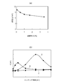
- 6A shows the relationship between the total pressure during film formation and the film density of the conductive film to be formed, and this relationship is suitable for the conductive films (60A, 60B) described above.
- the material shows the same tendency. Moreover, if the power at the time of sputtering or the distance between the substrate 1 and the sputtering target is in a general range, no particular dependency is observed.
- argon (Ar) gas, krypton (Kr) gas, xenon (Xe) gas, and the like can be used as the sputtering gas, but it is particularly preferable to use argon gas from the viewpoint of manufacturing cost.
- a DC power source or an RF power source having an industrial power frequency such as 13.56 MHz can be used as the sputtering power source.
- the power during sputtering is a value obtained by dividing the discharge power by the area of the target. As a general range, it can be set to, for example, 1 W / cm 2 or more and 5 W / cm 2 or less.
- the distance between the sputtering target and the substrate 1 can be set to, for example, 50 mm or more and 200 mm or less as a general range.
- the second conductive film may be formed between the side surface 3f and the upper surface 3e of the first insulating layer 3a between the step 3 and the step 4 under a pressure lower than the above pressure range.
- the second conductive film may be formed on the surface of the cathode 6 (at least the plurality of protrusions 16) formed through the step 5 under a pressure lower than the above pressure range.
- the process resistance of the cathode 6 and the stability during driving can be improved.
- the occurrence of the voltage drop described above can be suppressed even if the cathode 6 becomes high resistance through the step 5.
- the conductive film 60A and the conductive film 60B may be made of the same material or different materials. However, it is preferable that the conductive film 60A and the conductive film 60B are simultaneously formed of the same material from the viewpoint of ease of manufacture and controllability of etching. Further, the above-described second conductive film may be the same material as the conductive film 60A or may be a different material. However, it is preferable to form the film with the same material as that of the conductive film 60A because of ease of manufacture.
- the conductive film 60A and the conductive film 60B may be formed in contact with each other or may be formed without contact.
- the gap 8 can be formed by the step 5. Therefore, it is desirable to form the conductive film 60A and the conductive film 60B in contact with each other because the controllability of the gap 8 is improved.
- a conductive film is formed on the corner portion 32 of the first insulating layer 3a shown in FIG. 8C. Since it is necessary to deposit 60A, it is preferable to use a directional sputtering method.
- a shielding plate is provided between the substrate 1 and the target.
- a so-called collimation sputtering method using a collimator that gives directivity to the sputtered particles is also a category of the above-mentioned directivity sputtering method. In this way, only a limited number of sputtered particles (sputtered atoms or sputtered particles) are incident on the deposition surface.
- the incident angle of the sputtered particles (film forming material) to the inclined surface 3f of the first insulating layer 3a is smaller than the incident angle of the sputtered particles (film forming material) to the upper surface 3e (corner portion 32) of the first insulating layer 3a. It is preferable to make the angle (shallow). However, the incident angle of the sputtered particles with respect to the upper surface 3e of the first insulating layer 3a is set closer to 90 degrees than the incident angle of the sputtered particles with respect to the inclined surface 3f of the first insulating layer 3a.
- the sputtered particles can be incident on the upper surface 3e of the first insulating layer 3 in a state closer to the vertical than the inclined surface 3f of the first insulating layer 3.
- the protruding portion 16 can be formed with good controllability on the corner portion 32 of the first insulating layer 3a.
- the third etching process may be either dry etching or wet etching, but it is preferable to select wet etching in consideration of the ease of setting the etching selectivity with other materials.
- the combination of the material of the conductive films (60A, 60B) and the etchant used for the third etching process is not particularly limited.
- the material of the conductive films (60A, 60B) is molybdenum (Mo)
- TMAH tetramethylammonium hydroxide
- aqueous ammonia etchant
- a mixture of 2 (2-n-butoxyethoxy) ethanol and alkanolamine, DMSO (dimethyl sulfoxide), or the like can also be used as an etchant.
- the material of the conductive films (60A, 60B) is tungsten (W)
- nitric acid, hydrofluoric acid, sodium hydroxide solution, or the like is preferably used as the etchant.
- the film density and the etching rate are in an inversely proportional relationship.
- the etching rate means the amount of change in film thickness per unit time.
- the conductive films (60A, 60B) formed in the pressure range shown in step 4 include a crystal grain portion and a crystal grain boundary portion suitable for forming the significant protrusion 16. It is a conductive film. There is an etching selectivity between the crystal grain part and the crystal grain boundary part. Therefore, if the conductive film (60A, 60B) formed in the pressure range described above is subjected to the etching process in step 5, the crystal grain boundary part is preferentially etched compared to the crystal grain part. Yes. As a result, it is considered that the cathode 6 including the significant protrusion 16 mainly composed of the crystal grain portion can be formed. An image of this process is shown in FIG. Step 5 does not necessarily intend to remove all the crystal grain boundaries.
- FIG. 5B is a schematic diagram showing the relationship between the standard deviation ⁇ of the distance d between the cathode 6 and the gate 5 and the electron emission current Ie. As shown in FIG. 5B, there is a phenomenon in which the electron emission current Ie increases as ⁇ increases. From this phenomenon, it can be understood that, for the electron-emitting device, obtaining the protruding portion 16 capable of forming a large ⁇ leads to obtaining a large electron-emitting current Ie.
- the standard deviation ⁇ of the distance d is measured, for example, by measuring the distance d between the cathode and the gate 5 in the gap 8 along the direction in which the gap 8 extends (the direction in which the corner portion 32 of the insulating member 3 extends). To do. Specifically, the distance d is measured by observing the gap 8 with an SEM from the direction of the arrow in FIG. 4 (a) and 4 (b) schematically show a part of the gap 8 observed with an SEM from the direction of the arrow in FIG. 1 (b). 4A shows a schematic diagram when the gate does not include the conductive film 6B, and FIG. 4B shows a schematic diagram when the gate 5 includes the conductive film 6B. Yes. Then, the distance d of the gap 8 is sequentially measured along the direction in which the gap 8 extends (Y direction), and the standard deviation ⁇ can be obtained from the measured value.
- FIG. 6B is a graph showing a change in the distance d between the cathode 6 and the gate 5 with the lapse of etching time when the total pressure during sputtering is changed.
- the horizontal axis represents the etching time
- the vertical axis represents the standard deviation ⁇ of the distance d between the cathode 6 and the gate 5 in the gap 8.
- a curve indicated by A indicates a case where the total pressure is 1.7 Pa, and is a similar curve when the total pressure is 1.0 Pa or more and 2.8 Pa or less.
- the curve shown by B has shown the case where the total pressure is 3.0 Pa, and becomes a similar curve in the range where the total pressure is higher than 2.8 Pa.
- a curve indicated by C shows a case where the total pressure is 0.1 Pa, and is a similar curve when the total pressure is lower than 1.0 Pa.
- the characteristics shown in FIG. 6B show the same tendency in the materials suitable for the conductive films (60A, 60B) described above, and are particularly reproducible when Mo or W is used. In addition, the characteristics shown in FIG. 6B are not particularly dependent on the power during sputtering and the distance between the substrate 1 and the sputtering target in the general range as described above.
- the ⁇ is larger than that in the case where the film is formed at a pressure different from the pressure range described above. Can be obtained.
- the film is formed under a pressure smaller than the above-described pressure range, the tendency that ⁇ hardly changes even when the etching time in Step 5 is increased becomes remarkable. That is, the formation of the protruding portion 16 by the step 5 is not substantially performed. This is because, compared to the case where the film is formed in the above-described pressure range, a larger number of crystal grain portions are formed, so that the significant etching for forming the protruding portion 16 is not performed in Step 5. thinking.
- FIG. 5 (a) plots the maximum value of ⁇ obtained by etching in step 5 when the total pressure during sputtering is changed. As can be seen from this graph, a large ⁇ can be stably obtained within a pressure range of 1.0 Pa to 2.8 Pa in total pressure.
- the protrusion 16 capable of forming a large ⁇ is formed. It can be controlled and formed stably.
- the cathode electrode 2 has conductivity like the gate 5 and can be formed by a general vacuum film forming technique such as a vapor deposition method or a sputtering method, or a photolithography technique.
- the material of the cathode electrode 2 may be the same material as the gate 5 or a different material.
- the thickness of the cathode electrode 2 is set in the range of several tens of nm to several ⁇ m, and preferably selected in the range of several hundreds of nm to several ⁇ m.
- the cathode 6 includes a plurality of protrusions 16 provided side by side along a corner 32 (see FIG. 3), which is a boundary between the upper surface 3e of the insulating member 3 and the side surface 3f of the insulating member 3 (see FIG. 3). (Refer FIG.1 (c)).
- the protrusion 16 has a convex shape in the ZX plane as shown in FIG. 1B, and also has a convex shape in the ZY plane as shown in FIG. 1C.
- Each of the plurality of protruding portions 16 protrudes from the corner portion 32 of the insulating member 3 so as to be separated from the upper surface of the insulating member 3.
- FIG. 9 the electron beam emitting device described later using FIG. 9 and the display panel described later using FIG.
- each of the plurality of protruding portions 16 protrudes from the corner portion 32 of the insulating member 3 toward the anode described later. Yes. Therefore, it can be said that each of the plurality of protruding portions 16 protrudes along the direction in which the insulating member 3 is laminated on the substrate 1 or along the direction perpendicular to the surface of the substrate 1. .
- the distance between the periphery of the protrusion 16 and the gate 5 is larger than the distance between the protrusion 16 and the gate 5.
- the electrons emitted from the protrusions 16 are isotropically scattered at the gate 5, and among the scattered electrons, the electrons scattered on both sides of the protrusions 16 are portions where the distance from the gate 5 is wide.
- the electron emission efficiency ⁇ can be improved as compared with the case where the cathode 6 is flat along the corner 32, that is, as compared with the case where the distance between the gate and the cathode is constant along the corner 32. it can.
- the end portion on the gate 5 side of the cathode 6 covers at least a part of the side surface (3f) side of the upper surface (3e) of the insulating member 3, as shown in FIGS.
- the plurality of projecting portions 16 constituting the end portion of the cathode 6 are corner portions 32 (see FIG. 1C) that are boundaries between the upper surface (3e) of the insulating member 3 and the side surface (3f) of the insulating member 3. )
- each of the plurality of protrusions 16 of the cathode 6 covers a part of the side surface (3f) side of the upper surface (3e) of the insulating member 3.
- a part of the protrusion 16 of the cathode 6 enters the recess 7 of the insulating member 3 and a part of the protrusion 16 is connected to the upper surface of the insulating member 3.
- the tip When the protrusion 16 is enlarged, as shown in FIG. 3, the tip has a shape represented by a curvature radius r. Depending on the radius of curvature r, the electric field strength at the tip changes. As r is smaller, the lines of electric force are concentrated, so that a high electric field can be formed at the tip of the protrusion 16. Since the distance d between the gate 5 and the cathode 6 affects the difference in the number of electron scattering at the gate, the electron emission efficiency ( ⁇ ) can be increased as r is smaller and d is larger. From the viewpoint of suppressing the driving voltage Vf necessary for emitting electrons, the driving voltage increases if d is larger than 10 nm.
- d is preferably 1 nm or more. This is because if the thickness is smaller than 1 nm, the cathode protrusion 16 may be destroyed during driving due to field evaporation, discharge, short circuit, or the like. Therefore, practically, d is preferably 1 nm or more and 10 nm or less.
- the following four merits can be considered because the protruding portion 16 covers a part of the upper surface 3e of the insulating member 3.
- the first merit is that the projecting portion 16 serving as an electron emitting portion comes into contact with the insulating member 3 with a large area, so that the mechanical adhesion is increased (adhesion strength is increased).
- the second merit is that the thermal contact area between the projecting portion 16 serving as the electron emitting portion and the insulating member 3 is widened, and the heat generated in the electron emitting portion can be efficiently released to the insulating layer 3 ( Thermal resistance is reduced).
- the third merit is that the electric field strength at the triple point generated at the boundary between the insulator, the vacuum and the metal is weakened by contacting the upper surface of the insulating member 3 with a gentle inclination, and an abnormal electric field is generated. Thus, the possibility of occurrence of a discharge phenomenon can be suppressed.
- the fourth merit is that the electron emission efficiency is increased by making the surface of the protrusion 16 on the second insulating layer 3b side inclined with respect to the normal to the back surface 5b of the gate 5. .
- the protrusion 16 covers not only the side surface 3f of the insulating member 3 but also a part of the upper surface 3e of the insulating member 3 will be described in more detail.
- the time variation of initial Ie and Ie was measured by changing the length x of the end (protrusion 16) on the gate 5 side of the cathode 6 entering the recess 7 from the side surface 3f of the insulating member 3.
- the intrusion length x corresponds to x in FIG. 3 and can be regarded as the length of the protrusion 16 connected to the upper surface of the insulating member 3.
- Ie means the amount of emission current and corresponds to the amount of electrons reaching the anode 20 in FIG.
- the value of x is set to 10 nm or more and 30 nm or less.
- the value of x can be controlled by controlling the angle during deposition of the material of the cathode 6, the thickness of the second insulating layer 3 b, and the thickness of the gate 5.
- the value of x is larger than 30 nm, a leak occurs between the cathode 6 and the gate 5 via the upper surface of the insulating member 3, and the leak current increases.
- the tip of the protruding portion 16 of the cathode 6 be separated from the gate 5 as much as possible (the interval d is increased). By doing so, scattering of electrons in the gate 5 can be reduced, and as a result, the electron emission efficiency ⁇ and the emission current amount Ie can be improved.
- the gate 5 it is desirable to provide an offset amount Dx between the tip of the protruding portion 16 of the cathode 6 and the side surface 5b of the gate 5.
- the electron emission efficiency ⁇ (emission current amount Ie) can be improved, and at the same time, an invalid current (element current If) flowing through the gate 5 is reduced, so that thermal deformation of the gate is suppressed.
- stable electron emission can be realized.
- the triple point In general, the place where three types of materials with different dielectric constants such as vacuum, insulators, and metals are in contact with each other is called a triple point.
- the electric field strength at the triple point is extremely higher than the surroundings, it can cause discharge. There is. Therefore, if the angle ⁇ (see FIG. 3) at which the protrusion 16 and the upper surface of the insulating member 3 are in contact is greater than 90 degrees, there is no great difference from the surrounding electric field.
- the angle ⁇ is 90 degrees or less. It becomes.
- a strong electric field is formed in the part where the cathode 6 is peeled off, and electron emission occurs from this part, or the electron-emitting device may be destroyed by creeping discharge triggered by this electron emission. Therefore, a desirable angle of the angle ⁇ at which the protruding portion 16 of the cathode 6 and the upper surface of the insulating member 3 are in contact is greater than 90 degrees.
- a part (6b) which is a part of the cathode 6 and is located between each of the plurality of protrusions 16 is made to move electrons from the cathode electrode 2 toward the protrusions 16.
- a mode in which the resistance is higher than that of the other portion (6a) along the flow is desirable. More specifically, it is desirable that the resistance value between two adjacent protrusions of the plurality of protrusions 16 be larger than the resistance value between each protrusion 16 and the cathode electrode. By doing in this way, the mutual influence of the some protrusion parts 16 of the cathode 6 can be reduced.
- the resistance is increased by selectively oxidizing only the portion shown in 6b exposed in a state where the portion shown in 6a of the cathode 6 is masked. Can do.
- the method for increasing the resistance is not limited to oxidation, and the resistance can be increased by other known methods such as doping.
- a resistor is provided on all or part of the portion indicated by 6a in FIG. 2A (portion connecting the cathode electrode 2 and the protruding portion 16). This is preferable because a resistance can be individually provided for each electron emission portion (protrusion portion 16), and time variation of the emission current from each electron emission portion can be suppressed. Even in this case, the resistance value between two adjacent protrusions of the plurality of protrusions 16 is made larger than the resistance value between each protrusion 16 and the cathode electrode.
- the portion indicated by 6a in FIG. 2A is thicker than the portion indicated by 6b.
- the creepage distance between the several protrusion parts 16 used as an electron emission part is enlarged. can do.
- the portion indicated by 6b can have a higher resistance than the portion indicated by 6a. Therefore, as described above, the influence of the plurality of protrusions 16 on each other can be reduced. Can do.
- the part shown by 6b can be removed, and it can also be set as the aspect shown in FIG.2 (b).
- the cathode 6 has a portion indicated by 6b in addition to a portion essential for connecting each of the plurality of protrusions 16 and the cathode electrode 2 indicated by 6a.
- a portion indicated by 6b is a part of the side surface 3f of the insulating member 3, and a portion located between each of the plurality of projecting portions 16 is prevented from being exposed to vacuum and charged in the portion.
- FIG. 2B when the cathode 6 does not include the portion indicated by 6b, a part of the electrons emitted from the protrusion 16 and isotropically scattered by the gate 5 are insulated.
- the cathode 6 is positioned between each of the plurality of protrusions 16 in addition to the essential part (6a) for connecting each of the plurality of protrusions 16 and the cathode electrode 2. It is desirable to provide the part (6b) to do.
- the side surface 3f of the insulating member 3b as shown in FIG. 1 (C) and FIG.
- the cathode 6 also covers the portion located between them. By disposing a part of the cathode 6 between the plurality of protrusions 16 in this manner, charging of the surface of the insulating member 3 between each of the plurality of protrusions 16 can be suppressed, and electron emission can be stabilized. it can.
- a step of increasing the resistance of the cathode 6 may be performed after step 5.
- the resistance can be increased by lightly oxidizing the cathode 6.
- the method for increasing the resistance is not limited to oxidation, and the resistance can be increased by other known methods such as doping.
- the cathode electrode 2 is provided on the surface of the substrate 1, and the cathode 6 is provided on the cathode electrode 2 located immediately below the opening 30 of the gate 5.
- the gate 5 sandwiches the insulating member 3 between the substrate 1 and a circular opening 30.
- the cathode electrode 2 is also provided between the insulating member 3 and the substrate 1.
- the cathode electrode 2 need not be provided between the insulating member 3 and the substrate 1. Also good.
- the manufacturing method described above is applied to the electron-emitting device having such an aspect, first, the cathode electrode 2, the insulating member 3, and the gate 5 are stacked on the substrate 1, and then the opening 30 is formed in the gate. At the same time, an opening communicating with the opening 30 is formed in the insulating member 3. Then, by performing Step 4 and Step 5 described above, the electron-emitting device having the mode shown in FIG. 2C can be formed.
- the cathode electrode 2 corresponds to a substrate on which a conductive film made of a material constituting the cathode 6 is deposited.
- the substrate 1 and the cathode electrode 2 correspond to a substrate on which a conductive film made of a material constituting the cathode 6 is deposited.
- the electron emission characteristics can be measured with the configuration shown in FIG. In FIG.
- Vf is a voltage applied between the gate 5 and the cathode 6, and If is an element current flowing between the gate 5 and the cathode 6 when Vf is applied between the gate 5 and the cathode 6.
- Va is a voltage applied between the cathode 6 and the anode 20, and Ie is an electron emission current.
- a power source that applies a potential to the anode 20 and a power source that applies a potential to the cathode 6 may be provided separately. As shown in FIG.
- FIG. 10 (a) is a schematic view showing an example of a display panel 77 configured using an electron source in which electron-emitting devices are arranged in a matrix, and a part thereof is cut away so that the inside can be seen.
- 61 is an electron source substrate
- 62 is an X direction wiring
- 63 is a Y direction wiring.
- the electron source substrate 61 corresponds to the substrate 1 of the electron-emitting device described above.
- Reference numeral 64 schematically shows the above-described electron-emitting device.
- the X-direction wiring 62 is a wiring that commonly connects the cathode electrodes 2 described above
- the Y-direction wiring 63 is a wiring that commonly connects the gates 5 described above.
- the electron-emitting device is provided at the intersection of the X-direction wiring 62 and the Y-direction wiring 63 is shown schematically, but the electron-emitting device is an intersection of the X-direction wiring 62 and the Y-direction wiring 63.
- the electron source substrate On the side of the electron source substrate.
- the X direction wiring 62 is connected to a scanning signal applying means (not shown) for applying a scanning signal for selecting a row of the electron-emitting devices 64 arranged in the X direction.
- the Y direction wiring 63 is connected to a modulation signal generating means (not shown) for modulating each column of the electron-emitting devices 64 arranged in the Y direction according to an input signal.
- the drive voltage applied to each electron-emitting device is supplied as a difference voltage between the scanning signal and the modulation signal applied to the device.
- the electron source substrate 61 is fixed to the rear plate 71. Further, on the inner surface of the glass substrate 73, a light emitter 74 made of, for example, a phosphor that emits light when irradiated with electrons emitted from the electron-emitting device, and a metal back 75 corresponding to the anode 20 described above are laminated.
- the face plate 76 is configured. Further, the rear plate 71 and the face plate 76 are airtightly bonded to each other via a support frame 72 provided between the rear plate 71 and the face plate 76 and a bonding member such as frit glass, so that the display panel 77 is formed. It is configured.
- the display panel 77 includes the face plate 76, the support frame 72, and the rear plate 71.
- the rear plate 71 is provided mainly for the purpose of reinforcing the strength of the electron source substrate 61, if the electron source substrate 61 itself has sufficient strength, the separate rear plate 71 is not required. Can do.
- a support not shown
- a spacer between the face plate 76 and the rear plate 71 it is possible to provide a structure with sufficient strength against atmospheric pressure.
- the receiving circuit 20 includes a tuner, a decoder, and the like, receives various signals such as satellite broadcasting and terrestrial television signals, data broadcasting via a network, and outputs decoded video data to the image processing unit 21. To do.
- the “received signal” described above can be rephrased as “input signal”.
- the image processing unit 21 includes a ⁇ correction circuit, a resolution conversion circuit, an I / F circuit, and the like.
- the image processing unit 21 converts the image-processed video data into a display format of a display (image display device) 25 and puts it on the display (image display device) 25. Output as an image signal.
- the display 25 includes at least the display panel 77 described above, and further includes the drive circuit 108 and the control circuit 22 that controls the drive circuit 108 described above.
- the control circuit 22 performs signal processing such as correction processing on the input image signal and outputs the image signal and various control signals to the drive circuit 108.
- the control circuit 22 includes a synchronization signal separation circuit, an RGB conversion circuit, a luminance signal conversion unit, a timing control circuit, and the like.
- the drive circuit 108 outputs a drive signal to the electron-emitting devices inside the display panel 77 based on the input image signal, and a television image is displayed based on the drive signal.
- the drive circuit 108 includes a scanning circuit, a modulation circuit, a high-voltage power supply circuit that supplies an anode potential, and the like.
- the receiving circuit 20 and the image processing circuit 21 may be housed in a housing separate from the display 25 as a set-top box (STB 26), or may be housed in a housing integral with the display 25.
- STB 26 set-top box
- the television device 27 displays a television image.
- the receiving circuit 20 is a circuit that receives video distributed through a line such as the Internet
- the television device 27 functions as a video display device capable of displaying various videos as well as television videos. .
- Example 1 With reference to FIGS. 8A to 8F, a method of manufacturing the electron-emitting device of this example will be described.
- insulating layers 30 and 40 and a conductive layer 50 are stacked on the substrate 1.
- substrate 1 used the high strain point low sodium glass (Asahi Glass Co., Ltd. product PD200).
- a silicon nitride film was formed by a sputtering method, and the thickness thereof was set to 500 nm.
- a silicon oxide film was formed by a sputtering method, and its thickness was 30 nm.
- the conductive layer 50 is made of a tantalum nitride film, formed by sputtering, and has a thickness of 30 nm.
- the conductive layer 50, the insulating layer 40, and the insulating layer 30 were sequentially processed by using a dry etching method. .
- the conductive layer 50 and the insulating layer 30 are patterned to become the gate 5 and the first insulating layer 3a.
- a CF 4 gas is used as the etching gas at this time.
- the angle of the side surfaces after etching of the insulating layers (30, 40) and the gate 5 was formed at an angle of about 60 ° with respect to the surface (horizontal plane) of the substrate.
- the insulating layer 40 is formed using BHF (high purity buffered hydrofluoric acid LAL100 manufactured by Stella Chemifa Co., Ltd.) as shown in FIG. Was etched.
- the thickness on the slope 3f of the first insulating layer 3a is at least 35 nm on the slope 3f and the upper surface 3e of the first insulating layer 3a and on the gate 5.
- Mo molybdenum
- the substrate 1 was set so that the surface thereof was horizontal with respect to the sputter target.
- a shielding plate is provided between the substrate 1 and the target so that the sputtered particles are incident on the surface of the substrate 1 at a limited angle (specifically, 90 ⁇ 10 ° with respect to the surface of the substrate 1). Provided.
- the power of argon plasma at the time of sputtering was 1 W / cm 2
- the distance between the substrate 1 and the target was 100 mm
- the total pressure was 1.7 Pa.
- the conductive film 60A was formed so that the amount of the conductive film 60A entering the recess 7 (distance x in FIG. 3) was 35 nm.
- the conductive film 60A and the conductive film 60B were simultaneously formed.
- the conductive film 60A and the conductive film 60B were formed so as to be in contact with each other.
- a wet etching process (third etching process) was performed on the conductive film 60A and the conductive film 60B.
- TMAH tetramethylammonium hydride
- the conductive film 60A and the conductive film 60B were immersed in this etchant for 40 seconds, and then washed with running water for 5 minutes.
- the cathode electrode 2 was formed. Copper (Cu) was used as the material of the cathode electrode 2. A sputtering method was used as the production method, and the thickness was 500 nm.
- an anode electrode 20 was provided 1.7 mm above the electron-emitting device prepared in this example as shown in FIG. 9 and the electron emission characteristics were measured, it was applied between the cathode electrode 2 and the gate 5.
- the drive voltage Vf was 23 V
- the electron emission current Ie was 6 ⁇ A.
- Comparative Example 1 An electron-emitting device was produced in the same manner as in Example 1 except that the total pressure during sputtering in Example 1 was changed to 0.1 Pa.
- the electron emission current Ie was 1 ⁇ A when the drive voltage applied between the cathode electrode 2 and the gate 5 was 23V.
- the average value of the distance d of the gap 8 of the electron-emitting device of this comparative example is slightly smaller than the electron-emitting device of Example 1, and the standard deviation ⁇ of the distance d in the electron-emitting device of this comparative example is that of Example 1.
- the distance d between the protruding portion 16 and the gate 5 is substantially constant along the corner portion 32, and the corner portion 32 as shown in FIG. A plurality of significant protrusions 16 dotted along (in the Y direction) were not confirmed.
- Comparative Example 2 In Comparative Example 1, an electron-emitting device was produced in the same manner as in Example 1, except that the total pressure during sputtering in Example 1 was changed to 3.0 Pa.
- the electron emission current Ie was 1.5 ⁇ A when the drive voltage applied between the cathode electrode 2 and the gate 5 was 23V.
- the average value of the distance d of the gap 8 of the electron-emitting device of this comparative example is larger than that of the electron-emitting device of Example 1, and the standard deviation ⁇ of the distance d in the electron-emitting device of this comparative example is that of Comparative Example 1. It was larger than the standard deviation ⁇ of the distance d in the electron-emitting device. However, the standard deviation ⁇ in the electron-emitting device of this comparative example was smaller than the standard deviation ⁇ in the electron-emitting device of Example 1.
- Example 2 an electron-emitting device was fabricated basically in the same manner as in Example 1 except that the second conductive film was formed before forming the conductive films (60A, 60B). The second conductive film was also formed by sputtering Mo.
- the same sputtering conditions were used except that the total pressure during sputtering of the conductive film (60A, 60B) of Example 1 was 0.1 Pa.
- the film was formed so as to have a film thickness of 20 nm.
- the formed second conductive film was immersed in BHF (Stella Chemifa Co., Ltd., high-purity buffered hydrofluoric acid LAL100) for 30 seconds, and then washed with running water for 5 minutes.
- BHF tella Chemifa Co., Ltd., high-purity buffered hydrofluoric acid LAL100
- conductive films (60A, 60B) were formed to a thickness of 20 nm under the same conditions as in Example 1. Thereafter, the same process as in Example 1 was performed to produce the electron-emitting device of this example.
- Example 3 an electron-emitting device was fabricated basically in the same manner as in Example 1 except that the second conductive film was formed after the conductive films (60A, 60B) were formed. The second conductive film was also formed by sputtering Mo.
- the conductive films (60A, 60B) were formed to a thickness of 20 nm under the same conditions as in Example 1, and thereafter the same etching treatment as in Example 1 was performed.
- a second conductive film was formed.
- the second conductive film in this example was formed to a thickness of 15 nm under the same conditions as the second conductive film formed in Example 2, but in this example, the second conductive film was formed.
- the etching process performed on the second conductive film in Example 2 was not performed. Thereafter, the cathode electrode 2 was formed in the same manner as in Example 1 to produce the electron-emitting device of this example.
- Example 4 In this example, an electron source in which the electron-emitting devices of Example 1 were arranged in a matrix was created, and a display panel was created using this. Specifically, on the rear plate 71 made of a glass substrate, 1080 row wirings and 3 ⁇ 1920 column wirings were formed by a screen printing method using a silver paste. Subsequently, an electron-emitting device was formed in the vicinity of each intersection of the row wiring and the column wiring by the same method as the manufacturing method of Example 1.
- 1080 ⁇ 3 ⁇ 1920 phosphors 74 (1080 rows ⁇ 1920 columns of pixels) are formed on the surface of the glass substrate 73, and a metal back 75 made of aluminum is laminated thereon to form a face plate. 76 was formed. Then, in the vacuum chamber, a support frame 72 provided with frit glass in advance is disposed between the rear plate 71 and the face plate 76, and between the rear plate 71 and the support frame and between the face plate 76 and the support frame. And hermetically sealed with frit glass. As a result, an FED display (display panel 77) in which the inside was maintained in a vacuum was formed. Then, when the television device 27 shown in FIG. 10B was formed using this display panel, a high-luminance image could be displayed over a long period of time.
Landscapes
- Engineering & Computer Science (AREA)
- Manufacturing & Machinery (AREA)
- Cold Cathode And The Manufacture (AREA)
- Cathode-Ray Tubes And Fluorescent Screens For Display (AREA)
Abstract
電子放出に寄与する突出部をより多く制御して形成すると共に、突出部を大面積に渡って簡易に制御して形成する。 カソードを構成する導電性材料からなる導電性膜を、全圧が1.0Pa以上2.8Pa以下で行うスパッタリング法によって、形成し、前記導電性膜に対してエッチング処理を行って、表面に複数の突出部を備えるカソードを形成する。
Description
本発明は、ディスプレイなどに用いられる電子放出素子に関する。
ディスプレイなどに用いられる電子放出素子として電界放出型の電子放出素子が知られている。特許文献1には、電界が集中する微細な突起部を備えた電界放出型の電子放出素子が開示されている。また、特許文献2には、導電性膜の表面に凹凸が設けられた電子放出素子が開示されている。また、特許文献3には、一対の導電性膜の間に絶縁層を備え、その絶縁層の表面に凹部を有する電子放出素子が開示されている。
電子放出特性を向上させる上で、電子放出点の数をより多く且つ制御して形成するためには、突出部を制御して形成することが重要となる。しかしながら、従来は、電子放出に寄与する突出部をより多く制御して形成することが不十分であったり、突出部を大面積に渡って簡易に制御して形成することが不十分であったりする場合があった。そこで、本発明は、良好な電子放出特性を得るために、微細な突出部を制御性よく簡易な方法で実現することのできる製造方法を提供することを目的とする。
複数の突出部を備えるカソードを有する電子放出素子の製造方法であって、前記カソードを構成する材料からなる導電性膜を、全圧が1.0Pa以上2.8Pa以下で行うスパッタリング法によって、基体の上に形成する工程と、前記導電性膜に対してエッチング処理を行うことにより、表面に複数の突出部を備えるカソードを形成する工程と、を少なくとも有することを特徴とする。
本発明によれば、微細な突出部を有し、良好な電子放出特性を備える電子放出素子を、制御性よく簡易な方法で形成することができる。
以下に図面を参照して、好適な実施の形態を例示的に詳しく説明する。ただし、この実施の形態に記載されている構成部品の寸法、材質、形状、その相対配置などは、特に特定的な記載がない限りは、本発明の範囲をそれらのみに限定する趣旨のものではない。
まず本実施形態に係る製造方法が好ましく適用される電子放出素子の一例について図1(a)~図1(c)、図3を用いて説明する。
図1(a)は電子放出素子の平面模式図であり、図1(b)は図1(a)におけるA-A線および図1(c)のA-A線での断面模式図である。図1(c)は図1(b)における矢印の方向から電子放出素子を眺めたときの側面図である。図3は、図1(b)における一部の拡大模式図である。
電子放出素子は、基板1の表面に積層された絶縁部材3と、基板1との間に絶縁部材3を挟むように、絶縁部材3の上面に設けられたゲート5を備えている。更に、絶縁部材3の側面に設けられたカソード6を備えており、カソード6は、その一部が絶縁部材3の上面の一部にまで延在し、複数の突出部16を有している。複数の突出部16は絶縁部材3の側面(図1(b)においては3f)と上面(図1(b)においては3e)との境界部である角部32に沿って並んで設けられている。この複数の突出部16の各々が電子放出部に相当する。また、ゲート5とカソード6の突出部16との間には空隙である間隙8が形成されている。そして、カソード6とゲート5との間に、ゲート5の電位がカソード6の電位よりも高くなるように電圧を印加することで、カソード6の複数の突出部16から電子が電界放出される。尚、ゲート5の配置位置は、図1(a)~図1(c)に示す形態に限られるものではない。即ち、電子放出部である複数の突出部16に電界放出可能な電界を印加することができるように、カソード6と所定の間隔を置いて、配置されればよい。また、ここで示す例では、絶縁部材3を第1絶縁層3aと第2絶縁層3bとの積層体で構成した態様を示しているが、絶縁部材3は、1つの絶縁層で構成することもできる。また、絶縁部材3は、3つ以上の複数の絶縁層から構成することもできる。そして、図1(a)~図1(c)に示す態様では、第1絶縁層3aの上面3eの一部の上に第2絶縁層3bが積層している。即ち、第2絶縁層3bの側面3dを第1絶縁層3aの側面3fよりもカソード6から離れるように設けている。このようにすることで、絶縁部材3の上面が凹部7を備えることができる。このため、絶縁部材3の上面は段差を備えることになる。
次に、上記態様の電子放出素子を例に、本実施形態の製造方法の一連の工程を図8(a)~図8(f)を用いて簡単に説明し、その後、各工程について詳述する。
(工程1)
第1絶縁層3aとなる絶縁層30を基板1の表面に形成し、続いて、第2絶縁層3bとなる絶縁層40を絶縁層30の上面に積層する。そして、絶縁層40の上面にゲート5となる導電層50を積層する(図8(a))。
第1絶縁層3aとなる絶縁層30を基板1の表面に形成し、続いて、第2絶縁層3bとなる絶縁層40を絶縁層30の上面に積層する。そして、絶縁層40の上面にゲート5となる導電層50を積層する(図8(a))。
絶縁層40の材料は、絶縁層30の材料よりも、後述する工程3で用いるエッチング液(エッチャント)に対するエッチング量が多くなるように、絶縁層30の材料とは異なる材料が選択される。
(工程2)
次に、導電層50、絶縁層40、絶縁層30に対するエッチング処理(第1エッチング処理)を行う(図8(b))。
次に、導電層50、絶縁層40、絶縁層30に対するエッチング処理(第1エッチング処理)を行う(図8(b))。
第1エッチング処理は、具体的には、フォトリソグラフィー技術等により導電層50上にレジストパターンを形成したのち、導電層50、絶縁層40、絶縁層30をエッチングする処理である。工程2により、基本的には、図1(a)~図1(c)に示した電子放出素子を構成する第1絶縁層3aとゲート5が形成される。尚、図8(b)に示す様に、この工程で形成される第1絶縁層3aの側面(斜面)3fと基板1の表面とが成す角度(θ)を90°よりも小さくすることが好ましい。また、ゲート5の側面(斜面)5aと第1絶縁層3aの上面3e(又は基板1の表面)とが成す角度が、第1絶縁層3aの側面(斜面)3fと基板1の表面とが成す角度(θ)よりも小さくすることが好ましい。
(工程3)
続いて、絶縁層40に対するエッチング処理(第2エッチング処理)を行う(図8(c))。
続いて、絶縁層40に対するエッチング処理(第2エッチング処理)を行う(図8(c))。
工程3により、基本的には、図1(a)~図1(c)に示した電子放出素子を構成する第2絶縁層3bが形成される。この結果、第1絶縁層3aの上面3eの一部と第2絶縁層3bの側面3dとからなる凹部7が形成される。より詳細には、ゲート5の下面の一部と第1絶縁層3aの上面3eの一部と第2絶縁層3bの側面3dとで凹部7が形成される。また、工程3において、絶縁層40の側面がエッチングされるので第1絶縁層3aの上面3eの一部が露出する。第1絶縁層3aの上面3eと第1絶縁層3aの側面3fとが接続している部分(上面3eと側面3fの境界部)が角部32である。この工程により、後述する導電性膜60Aを堆積させる基体が形成される。即ち、本実施形態では、絶縁部材3が、あるいは、基板1と絶縁部材3とが、導電性膜60Aを堆積させる基体に相当する。
(工程4)
カソード6を構成する導電性材料からなる導電性膜60Aを、少なくとも第1絶縁層3aのカソード電極2側の側面となる斜面3fから、第1絶縁層3aの上面3eの一部に至るようにスパッタリング法により堆積する(図8(d))。
カソード6を構成する導電性材料からなる導電性膜60Aを、少なくとも第1絶縁層3aのカソード電極2側の側面となる斜面3fから、第1絶縁層3aの上面3eの一部に至るようにスパッタリング法により堆積する(図8(d))。
尚、この時、詳しくは後述するが、全圧が1.0Pa以上2.8Pa以下の条件下で、スパッタリング法により導電性膜60Aを成膜する。この条件で成膜することで、後述する工程5におけるエッチングによって有意な突出部16を形成するのに適した、結晶粒部分と結晶粒界部分とを備える導電性膜60Aを形成できる。
尚、導電性膜60Aは、第1絶縁層3aの角部32の少なくとも一部を覆い、第1絶縁層3aの側面3fから第1絶縁層3の上面3eにかけて延在するように成膜される。また、同時に、カソード6を構成する材料からなる導電性膜60Bも、ゲート5の上に堆積する。尚、図8(d)では、導電性膜60Aと導電性膜60Bとが接触するように成膜した例を示しているが、導電性膜60Aと導電性膜60Bとが接触しないように、導電性膜60Aと導電性膜60Bを成膜する場合もある。
(工程5)
続いて、少なくとも導電性膜60Aに対してエッチング処理(第3エッチング処理)を行い、カソード6を形成する(図8(e))。
続いて、少なくとも導電性膜60Aに対してエッチング処理(第3エッチング処理)を行い、カソード6を形成する(図8(e))。
第3エッチング処理は、複数の突出部16を形成することを主眼とした処理である。尚、工程4で導電性膜60Aと導電性膜60Bとを接触するように成膜した場合には、本工程により、その間に間隙8が形成される。また、工程4で導電性膜60Aと導電性膜60Bとを接触しないように成膜した場合には、本工程により、間隙8におけるゲート5とカソード6との距離dが広げられる。
工程5により、図1(c)に示すように、第1絶縁層3aの角部32に沿って、複数の突出部16が形成される。また、工程5により、凹部7内に付着している余計な導電材料を除去することもできる。これらの結果、カソード6と導電性膜6Bとが形成される。尚、工程5では、導電性膜(60A、60B)の露出している表面が全てエッチャントに曝されることになる。また、導電性膜6Bは残さずに除去しても良い。導電性膜6Bを除去する場合は、例えば、工程4の前にゲート5の表面に犠牲層を設け、犠牲層と共に導電性膜6Bを除去すればよい。
(工程6)
カソード6に電子を供給するためのカソード電極2を形成する(図8(f))。この工程は、他の工程の前や後に変更することもできる。尚、カソード電極2を用いずに、カソード電極2の機能をカソード6が兼ねることもできる。その場合には、工程6は省略できる。
カソード6に電子を供給するためのカソード電極2を形成する(図8(f))。この工程は、他の工程の前や後に変更することもできる。尚、カソード電極2を用いずに、カソード電極2の機能をカソード6が兼ねることもできる。その場合には、工程6は省略できる。
基本的には、以上の(工程1)~(工程6)により、図1(a)~図1(c)に示した複数の突出部16を備えるカソード6を有する電子放出素子を形成することができる。
尚、工程4においてゲート5の上に堆積した導電性膜60Bを完全に除去せずにゲート5の上に導電性膜6Bとして残す場合には、残った導電性膜6Bはゲート5の一部と見なすことができる。
また、工程5以降にカソード6を高抵抗化する工程を備える場合には、例えば、工程5以降にカソード6を酸化することでカソード6を高抵抗化することができる。
以下、各工程について詳細に説明する。
(工程1について)
基板1は電子放出素子を支持するための基板である。石英ガラス,Na等の不純物含有量を減少させたガラス、青板ガラスなどを用いることができる。基板1に必要な機能としては、機械的強度が高いだけでなく、ドライエッチング、ウェットエッチング、現像液等のアルカリや酸に対して耐性があることが挙げられる。また、画像表示装置に用いる場合は、加熱工程などを経るので、積層する部材と熱膨張率差が小さいものが望ましい。また熱処理を考慮すると、ガラス内部からのアルカリ元素等が電子放出素子に拡散しづらい材料が望ましい。
基板1は電子放出素子を支持するための基板である。石英ガラス,Na等の不純物含有量を減少させたガラス、青板ガラスなどを用いることができる。基板1に必要な機能としては、機械的強度が高いだけでなく、ドライエッチング、ウェットエッチング、現像液等のアルカリや酸に対して耐性があることが挙げられる。また、画像表示装置に用いる場合は、加熱工程などを経るので、積層する部材と熱膨張率差が小さいものが望ましい。また熱処理を考慮すると、ガラス内部からのアルカリ元素等が電子放出素子に拡散しづらい材料が望ましい。
絶縁層30(第1絶縁層3a)と絶縁層40(第2絶縁層3b)を構成する材料は、加工性に優れる材料からなり、たとえば窒化シリコン(典型的にはSi3N4)や酸化シリコン(典型的にはSiO2)である。絶縁層30と絶縁層40は、スパッタ法等の一般的な真空成膜法、CVD法、真空蒸着法で形成することができる。また絶縁層30の厚さは、数nmから数十μmの範囲で設定され、好ましくは数十nmから数百nmの範囲に選択される。また絶縁層40の厚さは、絶縁層30よりも薄く、数nmから数百nmの範囲で設定され、好ましくは数nmから数十nmの範囲で選択される。
尚、絶縁層30と絶縁層40を基板1上に積層した後に工程3にて凹部7を形成する場合は、上記第2エッチング処理に対して、絶縁層30よりも絶縁層40の方がよりエッチング量が多い関係に設定する。望ましくは絶縁層30と絶縁層40との間のエッチング量の比は、10以上であることが好ましく、50以上であることが更に好ましい。
このようなエッチング量の比を得るためには、例えば、絶縁層30を窒化シリコン膜で形成し、絶縁層40を酸化シリコン膜やリン濃度の高いPSGやホウ素濃度の高いBSG膜等で構成すれば良い。尚、PSGはリンシリケートガラスであり、BSGはボロンシリケートガラスである。
導電層50(ゲート5)は導電性を有しており、蒸着法、スパッタ法等の一般的真空成膜技術により形成されるものである。ゲート5となる導電層50の材料は、導電性に加えて高い熱伝導率があり、融点が高い材料が望ましい。例えば、Be,Mg,Ti,Zr,Hf,V,Nb,Ta,Mo,W,Al,Cu,Ni,Cr,Au,Pt,Pd等の金属またはこれらの合金材料が使用できる。また、炭化物や硼化物や窒化物も使用できる。また、導電層50(ゲート5)の厚さは、数nmから数百nmの範囲で設定され、好ましくは数十nmから数百nmの範囲で選択される。ゲート5となる導電層50は、カソード電極2に比べてその膜厚が薄い範囲で設定される場合があるので、カソード電極2の材料よりも低抵抗な材料であることが望ましい。
(工程2について)
上記第1エッチング処理では、エッチングガスをプラズマ化して材料に照射することで材料の精密なエッチング加工が可能な、RIE(Reactive Ion Etching)を用いることが好ましい。
上記第1エッチング処理では、エッチングガスをプラズマ化して材料に照射することで材料の精密なエッチング加工が可能な、RIE(Reactive Ion Etching)を用いることが好ましい。
RIEに用いるガスとしては、加工する対象部材がフッ化物を作る材料である場合には、CF4やCHF3やSF6などのフッ素系ガスが選ばれる。また加工する対象部材がSiやAlのような塩化物を形成する材料である場合には、Cl2、BCl3などの塩素系ガスが選ばれる。またレジストとの選択比を取るため、またエッチング面の平滑性の確保あるいはエッチングスピードを上げるため、水素、酸素、アルゴンガスの少なくともいずれかをエッチングガスに添加することが好ましい。
工程2により、基本的に、図1(a)~図1(c)に示した第1絶縁層3a及びゲート5と同一または略同一の形状が形成される。しかしながら、工程2以降に行われる各種のエッチング処理で、第1絶縁層3aとゲート5が全くエッチングされないことを意味する訳ではない。
また、第1絶縁層3aの側面(斜面)3fと基板1の表面とが成す角度(図8(b)にθで表示)は、ガス種、圧力、等の条件を制御することに所望の値に制御可能である。θは、90°よりも小さい角度とすることが好ましい。θを90°よりも小さい角度に設定することで、結果としてゲート5のカソード電極2側の側面5aは、第1絶縁層3aのカソード電極2側の側面3fよりも後退させることができる。また、ゲート5の側面(斜面)5aと第1絶縁層3aの上面3e(又は基板1の表面)とが成す角度が、第1絶縁層3aの側面(斜面)3fと基板1の表面とが成す角度よりも小さくすることが好ましい。尚、第1絶縁層3aの上面3eと第1絶縁層3aの側面3fとの成す角度は、180°-θとみなせる。尚、θは、第1絶縁層3aの側面3fにおいて、角部32から基板1方向へ接線を引いたときに、この接線と基板1とのなす角度で表すことができる(図8(b)参照)。
また、絶縁層3aは基板1の表面に一般的に用いられる成膜方法によって形成されているので、絶縁層3aの上面3eは基板1の表面と平行(実質的に平行)であると言える。即ち、絶縁層3aの上面3eは基板1の表面と完全に平行である場合もあるが、成膜環境や条件などにより、通常、僅かに傾きを有する場合が考えられるので、このような場合も含めて、平行の範疇である。
(工程3について)
工程3では、エッチング液(エッチャント)によって絶縁層40がエッチングされる量に対して、エッチング液によって絶縁層3aがエッチングされる量が十分に低くなるようにエッチング液が選択される。
工程3では、エッチング液(エッチャント)によって絶縁層40がエッチングされる量に対して、エッチング液によって絶縁層3aがエッチングされる量が十分に低くなるようにエッチング液が選択される。
上記第2エッチング処理は、例えば絶縁層40が酸化シリコンで形成され、第1絶縁層3a(絶縁層30)が窒化シリコンで形成されている場合、エッチング液は通称バッファードフッ酸(BHF)を用いればよい。バッファードフッ酸(BHF)はフッ化アンモニウムとフッ酸との混合溶液である。また、絶縁層40が窒化シリコンで形成され第1絶縁層3a(絶縁層30)が酸化シリコンで形成されている場合は、エッチャントは熱リン酸系エッチング液を使用すればよい。
工程3により、図1(a)~図1(c)に示した第2絶縁層3bと同一または略同一のパターンが形成される。しかしながら、工程3以降に行われるエッチング処理で、第2絶縁層3bが全くエッチングされないことを意味する訳ではない。
凹部7の深さ(奥行き方向の距離)は、電子放出素子のリーク電流に深く関わる。凹部7を深く形成するほどリーク電流の値が小さくなる。しかし、あまり凹部7を深くするとゲート5が変形する等の課題が発生する。このため、実用的には30nm以上200nm以下に設定される。尚、凹部7の深さは、絶縁層3aの側面3f(または角部32)から絶縁層3bの側面3dまでの距離と言い換えることもできる。
尚、絶縁部材3の上面3eと側面3fは直角に接続する形態に限定されず、鈍角で接続する形態とすることができる。また、図3のように、絶縁部材3の上面と側面とが接続する接続部(上面と側面の境界部)である角部32が、所定の曲率を有する形態とすることもできる。尚、絶縁部材3が、第1絶縁層3aと第2絶縁層3bとで構成される場合には、第1絶縁層3aの側面が絶縁部材3の側面に相当する
(工程4について)
導電性膜(60A、60B)は、カソード6を構成する材料をスパッタリング法により成膜することで形成される。
(工程4について)
導電性膜(60A、60B)は、カソード6を構成する材料をスパッタリング法により成膜することで形成される。
導電性膜(60A、60B)の材料(即ちカソード6を構成する材料)は、導電性があり、電子を電界放出することのできる材料であればよく、好ましくは、2000℃以上の高融点の材料から選択される。また、導電性材料は、5eV以下の仕事関数材料であり、その酸化物が簡易にエッチング可能な材料で形成されることが好ましい。このような導電性材料の好適な例として、例えば、Hf,V,Nb,Ta,Mo,W,Au,Pt,Pd等の金属またはこれらの合金材料が挙げられる。工程5におけるエッチング処理を行うことを考慮すると、導電性材料は、MoまたはWを用いることが特に好ましい。
導電性膜(60A、60B)のスパッタリング法による成膜は、1.0Pa以上2.8Pa以下の全圧下で行う。
このような成膜を行うことで、膜密度が高い領域(結晶粒部分)と膜密度が低い領域(結晶粒界部分)とを備える導電性膜を制御して形成することができる。尚、導電性膜(60A、60B)の密度や組成の測定は、一般にはXRR、XPSなどが用いられるが、実際の電子放出素子では測定が困難な場合がある。そのような場合には、密度や組成の測定手法として、例えば、以下の方法を採用することができる。即ち、TEM(透過電子顕微鏡)とEELS(電子エネルギー損失分光)を組み合わせた高分解能電子エネルギー損失分光電子顕微鏡で、元素の定量分析を行い、密度や組成を算出することができる。
図6(a)に示すように、スパッタ時の全圧を変化させて導電性膜(60A、60B)の成膜を行ったところ、1.0Paを境に、膜密度の減少率が急激に低下することがわかった。このように、上記圧力範囲よりも低い圧力下で成膜した場合に比べ、上記圧力範囲で成膜した導電性膜の膜密度は低くなる(結晶粒界部分が多くなる)。そのため、上記圧力範囲で成膜した導電性膜(60A、60B)に対して工程5の第3エッチング処理を行うと、工程5による有意な突出部16を簡易に制御して形成することができる。尚、図6(a)は成膜時の全圧と、形成される導電性膜の膜密度との関係を示しており、この関係は、前述した導電性膜(60A、60B)に好適な材料では同様の傾向を示す。また、スパッタリング時のパワーや、基板1とスパッタターゲットとの距離などが一般的な範囲であれば、特段の依存性は見られない。
尚、スパッタガスとしてはアルゴン(Ar)ガス、クリプトン(Kr)ガス、キセノン(Xe)ガスなどを用いることができるが、特にアルゴンガスを用いる方が製造コストの面から望ましい。スパッタ電源としては、DC電源、あるいは13.56MHzなどの工業用電源周波数のRF電源が使用できる。スパッタリング時のパワーは、放電電力をターゲットの面積で除した値であり、一般的範囲としては、例えば、1W/cm2以上5W/cm2以下とすることができる。また、スパッタターゲットと基板1との距離は、一般的範囲としては、例えば、50mm以上200mm以下とすることができる。
また、工程3と工程4の間に、上記圧力範囲よりも低い圧力の下で、第1絶縁層3aの側面3fから上面3eに渡って、第2導電性膜を成膜する場合もある。このようにして、カソード6となる導電性膜60Aの下に高い膜密度を備える第2導電性膜を設けて形成した電子放出素子では、電子放出素子を駆動する配線やカソード電極2と、各突出部16(電子放出部)とを低抵抗に接続することができる。そのため、電子放出素子を駆動した際に電圧降下が発生して所定の電子放出電流Ieが得られないという事態を抑制することができる。また、導電性膜60Aの絶縁部材3への密着性を向上することができるという効果もある。
また、一方で、工程5を経て形成した、カソード6の表面(少なくとも複数の突出部16)に、上記圧力範囲よりも低い圧力の下で、第2導電性膜を成膜する場合もある。このようにして、カソード6の表面を膜密度が高い第2導電性膜で被覆することで、カソード6のプロセス耐性や駆動時の安定性を向上させることができる。また、同時に、工程5を経てカソード6が高抵抗になっても前述した電圧降下の発生を抑制することもできる。
導電性膜60Aと導電性膜60Bは、同一材料でも良いし、異なる材料でも構わない。しかしながら、製造の容易性、エッチングの制御性から、導電性膜60Aと導電性膜60Bは同一材料で同時に成膜することが好ましい。また、上記した第2導電性膜は、導電性膜60Aと同一材料でも良いし、異なる材料でも構わない。しかしながら、製造の容易性から、導電性膜60Aと同一材料で成膜することが好ましい。
また、本工程では、導電性膜60Aと導電性膜60Bとを接触させて形成しても良いし接触せずに形成しても良い。接触させて形成した場合には、工程5によって、間隙8を形成することができる。そのため、導電性膜60Aと導電性膜60Bとを接触して形成する方が間隙8の制御性が向上するので望ましい。
そして、図1(a)~図1(c)に示す態様の電子放出素子を形成する場合には、図8(c)に示す第1絶縁層3aの角部32の上に、導電性膜60Aを堆積させる必要があるために、指向性スパッタリング法を用いることが好ましい。
指向性スパッタでは、例えば、基板1とスパッタターゲットとの角度を設定した上で、基板1とターゲットの間に遮蔽板を設ける。スパッタ粒子に指向性を与えるコリメータを用いる、いわゆるコリメーションスパッタ法も上記指向性スパッタリング法の範疇である。このようにして、限られた角度のスパッタ粒子(スパッタされた原子またはスパッタされた粒子)のみが被成膜面に入射される様にする。特に、スパッタ粒子(成膜材料)の第1絶縁層3aの斜面3fに対する入射角度が、スパッタ粒子(成膜材料)の第1絶縁層3aの上面3e(角部32)に対する入射角度よりも小さい(浅い)角度になる様にすることが好ましい。但し、スパッタ粒子の第1絶縁層3aの上面3eに対する入射角度は、スパッタ粒子の第1絶縁層3aの斜面3fに対する入射角度よりも、90度に近く設定する。このようにすることで、スパッタ粒子は、第1絶縁層3の斜面3fに対してよりも第1絶縁層3の上面3eに対して、より垂直に近い状態で入射させることができる。このような成膜を行うことで、第1絶縁層3aの角部32上に突出部16を制御性よく形成できる。
(工程5について)
第3エッチング処理としてはドライエッチング、ウェットエッチングの何れでも構わないが、他材料とのエッチング選択比の設定の容易さを考慮して、ウェットエッチングを選択することが好ましい。
第3エッチング処理としてはドライエッチング、ウェットエッチングの何れでも構わないが、他材料とのエッチング選択比の設定の容易さを考慮して、ウェットエッチングを選択することが好ましい。
導電性膜(60A、60B)の材料と第3エッチング処理に用いるエッチャントの組み合わせは、特に限定されるものではない。しかしながら、例えば、導電性膜(60A、60B)の材料がモリブデン(Mo)であれば、エッチャントはTMAH(水酸化テトラメチルアンモニウム)やアンモニア水などのアルカリ溶液を用いることが好ましい。或は、エッチャントとして、2(2-n-ブトキシエトキシ)エタノールとアルカノールアミンの混合物やDMSO(ジメチルスルホキシド)等も用いることもできる。また、導電性膜(60A、60B)の材料がタングステン(W)の場合は、硝酸やフッ酸や水酸化ナトリウム溶液等をエッチャントとして用いることが好ましい。
エッチング処理で除去される単位時間当たりの原子数は、導電性膜(60A、60B)の材料とエッチング液で一意に決まるので、膜密度とエッチングレートは反比例の関係にある。上記エッチングレートとは、単位時間当たりの膜厚変化量を意味している。
また、前述したように、工程4に示した圧力範囲で成膜した導電性膜(60A、60B)は、有意な突出部16を形成するのに適する結晶粒部分と結晶粒界部分とを含む導電性膜である。そして、結晶粒部分と結晶粒界部分との間にはエッチングの選択比がある。そのため、前述した圧力範囲で成膜した導電性膜(60A、60B)に対して工程5のエッチング処理を行うと、結晶粒界部分が結晶粒部分に比べて優先的にエッチングされると考えている。そして、その結果、結晶粒部分を主体とした有意な突出部16を備えるカソード6が形成することができると考えている。このプロセスのイメージを図7に示す。尚、工程5は、結晶粒界部分を全て除去することを必ずしも意図するものではない。
図5(b)は、カソード6のゲート5との間隔dの標準偏差σと電子放出電流Ieとの関係を示す模式図である。図5(b)に示すように、σが大きくなるにつれて電子放出電流Ieが大きくなる現象がある。この現象から、電子放出素子にとって、大きなσを形成することのできる突出部16を得ることが、大きな電子放出電流Ieを得ることに繋がることがわかる。
間隔dの標準偏差σは、例えば、間隙8におけるカソードとゲート5との間隔dを間隙8が延在する方向(絶縁部材3の角部32が延在する方向)に沿って測長することで行う。具体的には、間隔dの測長は、図1(b)の矢印の方向から間隙8をSEMにて観察して行う。図4(a)、図4(b)は間隙8を図1(b)の矢印の方向からSEMにて観察した際の一部の様子を模式的に示している。図4(a)は、ゲートが導電性膜6Bを備えていない場合の模式図を示しており、図4(b)はゲート5が導電性膜6Bを備えている場合の模式図を示している。そして、間隙8の延在する方向(Y方向)に沿って、間隙8の間隔dを順次測長し、この測長した値から標準偏差σを求めることができる。
また、カソード6とゲート5との間隔d(突出部16の形状)は、エッチング時間に対する依存性がある。図6(b)は、スパッタリング時の全圧を変えた時に、エッチング時間の経過による、カソード6とゲート5との間隔dの変化を示すグラフである。横軸はエッチング時間を表しており、縦軸は、間隙8におけるカソード6のゲート5との間隔dの標準偏差σを表している。図6(b)において、Aで示す曲線は、全圧が1.7Paの場合を示しており、全圧が1.0Pa以上2.8Pa以下の範囲では似通った曲線となる。また、Bで示す曲線は、全圧が3.0Paの場合を示しており、全圧が2.8Paよりも高い範囲では似通った曲線となる。また、Cで示す曲線は、全圧が0.1Paの場合を示しており、全圧が1.0Paよりも低い範囲では似通った曲線となる。
図6(b)に示す特性は、前述した導電性膜(60A、60B)に好適な材料では同様の傾向を示し、MoやWの時に特に再現性よく発現する。また、図6(b)に示す特性は、スパッタリング時のパワーや、基板1とスパッタターゲットとの距離などが、前述したような一般的な範囲であれば、特段の依存性は見られない。
図6(b)に示すように、全圧が1.0Pa以上2.8Pa以下の圧力範囲で成膜した場合は、上述した圧力範囲とは異なる圧力で成膜した場合に比べて、大きなσを得ることができる。
一方、上述した圧力範囲よりも大きな圧力下で成膜した場合は、σの変化がエッチング時間に対してより敏感になり、上述した圧力範囲で成膜した場合に比べて、制御性が劣る傾向が顕著になる。これは、上述した圧力範囲で成膜した場合に比べて、結晶粒界部分が多く形成されるために、工程5のエッチングによる突出部16の形成を、安定に且つ制御して行うことが困難になるためであると考えている。また、得られるσの最大値も、上述した圧力範囲で成膜した場合に比べて小さな値となる。
また、上述した圧力範囲よりも小さな圧力下で成膜した場合は、工程5のエッチング時間を増やしてもσはほとんど変化しなくなる傾向が顕著になる。つまり、工程5による突出部16の形成は実質的に行われない。これは、上述した圧力範囲で成膜した場合に比べて、結晶粒部分が多く形成されるために、工程5によって、突出部16を形成するための有意なエッチングが行われないためであると考えている。
図5(a)には、スパッタリング時の全圧を変えた時に、工程5のエッチングにより得られるσの最大値をプロットした。このグラフからわかるように全圧が1.0Pa以上2.8Pa以下の圧力範囲内で、大きなσを安定して得ることができる。
このように、工程4で示した圧力範囲で成膜した導電性膜(60A、60B)に対して、工程5で示したエッチングを行うことで、大きなσを形成することのできる突出部16を制御して安定に形成することができる。
(工程6について)
カソード電極2は、前記ゲート5と同様に導電性を有しており、蒸着法、スパッタ法等の一般的真空成膜技術、フォトリソグラフィー技術により形成することができる。カソード電極2の材料は、ゲート5と同じ材料であってもよく、異なる材料であってもよい。カソード電極2の厚さとしては、数十nmから数μmの範囲で設定され、好ましくは数百nmから数μmの範囲で選択される。
カソード電極2は、前記ゲート5と同様に導電性を有しており、蒸着法、スパッタ法等の一般的真空成膜技術、フォトリソグラフィー技術により形成することができる。カソード電極2の材料は、ゲート5と同じ材料であってもよく、異なる材料であってもよい。カソード電極2の厚さとしては、数十nmから数μmの範囲で設定され、好ましくは数百nmから数μmの範囲で選択される。
次に、上記製造方法により形成される電子放出素子の突出部16の周辺構造について説明する。
カソード6は、絶縁部材3の上面3eと絶縁部材3の側面3fとの境界部である、角部32(図3参照)に沿って並んで設けられた複数の突出部16を備えている(図1(c)参照)。突出部16は、図1(b)のように、Z-X平面において凸形状であると同時に、図1(c)に示すように、Z-Y平面においても凸形状である。複数の突出部16の各々は絶縁部材3の上面から離れるように、絶縁部材3の角部32から突出している。図9を用いて後述する電子線放出装置や図10(a)を用いて後述するディスプレイパネルでは、複数の突出部16の各々は絶縁部材3の角部32から後述するアノードに向かって突出している。そのため、複数の突出部16の各々は、基板1に絶縁部材3が積層される方向に沿って、あるいは、基板1の表面に対して垂直な方向に沿って、突出していると言うこともできる。
カソード6に突出部16を設けた場合、突出部16の周囲とゲート5との距離は、突出部16とゲート5との距離よりも広くなる。その結果、突出部16から放出された電子はゲート5で等方的に散乱するが、その散乱した電子のうち、突出部16の両脇に散乱した電子は、ゲート5との間隔が広い部分を抜けてアノードに到達することができる。従って、角部32に沿ってカソード6が平坦である場合と比べて、即ち、角部32に沿ってゲートとカソードとの間隔が一定の場合と比べて、電子放出効率ηを向上させることができる。
カソード6のゲート5側の端部は、図1(b)、図3に示すように、絶縁部材3の上面(3e)の側面(3f)側の少なくとも一部を覆っている。そして、カソード6の端部を構成する複数の突出部16は、絶縁部材3の上面(3e)と絶縁部材3の側面(3f)との境界部である角部32(図1(c)参照)に沿って並んでいる。そのため、カソード6の複数の突出部16の各々は、絶縁部材3の上面(3e)の側面(3f)側の一部を覆っていると言うことができる。或は、カソード6の突出部16の一部が絶縁部材3の凹部7内に入り込んでおり、且つ、絶縁部材3の上面に突出部16の一部が接続していると言うことができる。
突出部16を拡大すると、図3に示すように、その先端部は曲率半径rで代表される形状を有する。この曲率半径rに依存して、先端部の電界強度が変化する。rが小さいほど電気力線の集中が生じるため突出部16の先端に高い電界を形成することが可能となる。ゲート5とカソード6との間隔dは、ゲートでの電子の散乱回数の違いに影響するため、rが小さく、dが大きいほど電子放出効率(η)を高くすることができる。尚、電子を放出させるのに必要な駆動電圧Vfを抑える観点から、dが10nmより大きいと駆動電圧が高くなってしまう。また、駆動時の安定性の観点から、dが1nm以上となることが好ましい。1nmより小さいと、電界蒸発や放電、短絡などによりカソード突出部16が駆動時に破壊される可能性がある為である。そのため、実用的には、dは1nm以上10nm以下であることが好ましい。
突出部16が、絶縁部材3の上面3eの一部を覆っていることで、以下の4つのメリットが考えられる。1つ目のメリットは、電子放出部となる突出部16が絶縁部材3に広い面積を持って接触するので、機械的な密着力があがる(密着強度が上昇する)ことである。2つ目のメリットは、電子放出部となる突出部16と絶縁部材3との熱的な接触面積が広がり、電子放出部で発生する熱を効率よく絶縁層3に逃がすことが可能となる(熱抵抗が低減する)ことである。3つ目のメリットは、緩やかな傾斜を伴って絶縁部材3の上面と接触することで、絶縁体と真空と金属との境界で生じる三重点での電界強度を弱め、異常な電界が発生して放電現象が発生する可能性を抑制できることである。4つ目のメリットは、突出部16の第2絶縁層3b側の表面を、ゲート5の裏面5bに対する法線に対して傾斜させた形状とする事で、電子放出効率が増大することである。
ここで、突出部16が絶縁部材3の側面3fだけでなく絶縁部材3の上面3eの一部を覆っているメリットについてさらに詳細に説明する。
カソード6のゲート5側の端部(突出部16)の、絶縁部材3の側面3fから凹部7内への侵入する長さxを変化させて、初期のIeとIeの時間変動量を測定したところ、xの値が少なくなるにつれ、初期のIeからの低下量が大きくなる傾向があった。尚、侵入する長さxは、図3におけるxに相当し、絶縁部材3の上面と接続している突出部16の長さとみなすことができる。また、Ieとは、放出電流量を意味し、後述の図9におけるアノード20に到達する電子の量に相当する。
また、xの値が少ないほど初期のIeからの低下量が多かった。しかし、xの値が20nmを越えるとxの値に対する依存性が小さくなる傾向が見られた。
これらの結果から推察すると、xの値が増加することで、絶縁部材3に広い面積で突出部16が接触するため、熱抵抗が低減することが考えられる。更には、突出部16の体積増加による熱容量の増大などの作用も働いて、突出部16の先端の温度が低下することで初期変動が小さくなるのではないかと推察される。
尚、xの値は大きいほど良いという訳ではない。実用的にはxの値は10nm以上30nm以下に設定される。カソード6の材料の蒸着時の角度、第2絶縁層3bの厚さ、ゲート5の厚さを制御して、xの値を制御することができる。xの値を30nmよりも大きくすると、絶縁部材3の上面を介して、カソード6とゲート5との間のリークが発生し、リーク電流が増大する。
カソード6の突出部16の先端は、可能な限りゲート5から離す(間隔dを大きくする)ことが望ましい。このようにすることで、ゲート5における電子の散乱を減らし、結果、電子放出効率η並びに放出電流量Ieを向上させることができる。
また、図3に示すように、カソード6の突出部16の先端とゲート5の側面5bとの間に、オフセット量Dxを設けることが望ましい。言い換えると、カソード6の突出部(特にその先端)よりもゲート5の側面5aが、第2絶縁層3bの近くに位置するように、ゲート5を配置することが望ましい。これは、電子放出効率ηの向上(放出電流量Ieの向上)のため、および、電子放出の安定化のためである。突出部16の先端の真上にゲート5が存在しないことで、突出部16の先端から電界放出された電子がゲート5の裏面5bに衝突する可能性を低減することができる。その結果、電子放出効率η(放出電流量Ie)が向上することができるのと同時に、ゲート5に流れる無効な電流(素子電流If)が低減されるためにゲートの熱的な変形などが抑制されて安定な電子放出を実現することができる。
次に、三重点について述べる。一般に真空、絶縁体、金属の様に誘電率が異なる三種類の材料が接する場所は三重点と呼ばれ、三重点における電界強度が周囲よりも極端に高くなることで放電等の要因になる場合がある。そのため、突出部16と絶縁部材3の上面とが接する角度θ(図3参照)が90度よりも大きければ周囲の電界と大差がない。しかし、例えば、カソード6が、何らかの機械的強度不足により、絶縁部材3の上面から剥がれ、絶縁部材3の上面とカソード6との間に隙間が生じてしまった場合は、角度θが90度以下となる。この結果、カソード6の剥がれた部分に強大な電界が形成され、この部分から電子放出が生じる、あるいは、この電子放出が引き金となった沿面放電により電子放出素子の破壊が生じる場合がある。従って、カソード6の突出部16と絶縁部材3の上面とが接する角度θの望ましい角度は90度よりも大きい角度である。
次に、上述した本実施形態の製造方法を適用して形成される電子放出素子の変形例について説明する。
電子放出特性の安定化、特に放出電流の安定化のためには、カソード6の複数の突出部16同士が、互いに影響を及ぼすことを低減することが望ましい。
そこで、図2(a)に示すように、カソード6の一部であって、複数の突出部16の各々の間に位置する部分(6b)を、カソード電極2から突出部16に向かう電子の流れに沿って、その他の部分(6a)よりも高抵抗とする態様が望ましい。より詳細には、各突出部16とカソード電極との間の抵抗値よりも、複数の突出部16の隣り合う2つの突出部の間の抵抗値を大きくする態様が望ましい。このようにすることで、カソード6の複数の突出部16同士の相互の影響を低減することができる。6bに示す部分を高抵抗とする方法としては、例えば、カソード6の6aに示す部分にマスクを施した状態で露出する6bに示す部分のみを選択的に酸化することで高抵抗化を行うことができる。尚、高抵抗化の方法は酸化に限定されず、ドーピングするなどその他の周知の方法によっても高抵抗化を行うことができる。
上記態様に加えて、図2(a)における6aで示された部分(カソード電極2と突出部16を繋ぐ部分)の全てまたは一部に抵抗体を設けた態様とすることが望ましい。このようにすれば、各電子放出部(突出部16)毎に個別に抵抗を備えさせることができ、各電子放出部からの放出電流の時間変動が抑制できるので好ましい。尚、この態様の場合にも、各突出部16とカソード電極との間の抵抗値よりも、複数の突出部16の隣り合う2つの突出部の間の抵抗値を大きくする。
また、絶縁層3の側面3fが平坦である場合には、図2(a)における6aで示された部分を6bで示された部分よりも膜厚を厚くすることが望ましい。このようにすることで、6aで示された部分の膜厚と6bで示された部分の膜厚を等しくした場合に比べ、電子放出部となる複数の突出部16の間の沿面距離を大きくすることができる。また、同時に、6bで示された部分を6aで示された部分よりも高抵抗にすることができるので、前述したように、複数の突出部16同士が、互いに影響を及ぼすことを低減することができる。さらには、6bで示した部分を取り除いて、図2(b)に示す態様とすることもできる。この態様では、6bで示した部分がないので、複数の突出部16同士の影響が一層低減できる。また、6aで示した部分の各々が備える突出部16の数は、図2(a)では1つとして示したが、図2(b)のように、複数備えることもできるが。しかしながら、複数の突出部16同士の干渉(影響)を低減するためには、6aで示した部分の各々が備える突出部16の数は1つとするのが望ましい。
図2(a)で示した態様では、6aで示された、複数の突出部16の各々とカソード電極2とを接続するために必須の部分以外に、6bで示された部分をカソード6が備えている。6bで示した部分は、絶縁部材3の側面3fの一部であって、複数の突出部16の各々の間に位置する部分が、真空中に露出して当該部分が帯電することを抑制する役割を持つ。図2(b)に示すように、6bで示された部分をカソード6が備えていない場合には、突出部16から放出されてゲート5で等方的に散乱した電子の一部が、絶縁部材3の側面3fの一部であって複数の突出部16の各々の間に位置する部分を帯電させる。その結果、電子の放出が不安定になったり、放出された電子の軌道が経時的に変動したりすることが考えられる。そのため、図2(a)の様に、カソード6は、複数の突出部16の各々とカソード電極2とを接続する必須の部分(6a)以外に、複数の突出部16の各々の間に位置する部分(6b)を備えることが望ましい。また、絶縁部材3bの側面3fだけでなく、図1(C)や図2(a)に示すように、絶縁部材3の角部32の一部であって、隣り合う2つの突出部16の間に位置する部分をも、カソード6が覆うことが望ましい。このように複数の突出部16の間にカソード6の一部分を配置することで、複数の突出部16の各々の間に絶縁部材3の表面の帯電を抑制でき、電子放出を安定にすることができる。
また、図2(a)の6bで示した部分だけでなく、単に、突出部16を含めて、導電性膜6を高抵抗にするだけでも、放出電流の安定化に寄与する。そのためには、例えば、工程5以降にカソード6を高抵抗化する工程を行えば良い。例えば、カソード6を軽く酸化することで高抵抗化を行うことができる。尚、高抵抗化の方法は酸化に限定されず、ドーピングするなどその他の周知の方法によっても高抵抗化を行うことができる。
以上説明した例では、電子放出素子としてカソード6を絶縁部材3の側面に設けた態様を説明した。しかしながら、本実施形態の製造方法が適用される電子放出素子の態様は、このような態様に限定されるものではない。例えば、図2(c)のように、基板1の表面にカソード電極2が設けられており、ゲート5の開孔30の直下に位置するカソード電極2の上にカソード6が設けられた態様でもよい。尚、ゲート5は、基板1との間に絶縁部材3を挟んでおり、円形の開孔30を備えている。図2(c)ではカソード電極2が絶縁部材3と基板1との間にも設けられているが、カソード6に電子を供給できれば良いので、絶縁部材3と基板1との間に設けなくても良い。このような態様の電子放出素子に上述した製造方法を適用する場合には、まず、基板1上にカソード電極2と絶縁部材3とゲート5とを積層した後に、ゲートに開孔30を形成すると共に絶縁部材3に開孔30と連通する開孔を形成する。そして、その後に、前述した工程4と工程5を行うことで、図2(c)に示した態様の電子放出素子を形成することができる。尚、この態様の場合には、カソード電極2がカソード6を構成する材料からなる導電性膜を堆積させる基体に相当する。或は、基板1とカソード電極2がカソード6を構成する材料からなる導電性膜を堆積させる基体に相当する。
次に、本実施形態の製造方法によって製造された電子放出素子の電子放出特性の測定方法と、カソード6から放出された電子のアノードへの到達効率、即ち、電子放出効率(η)について説明する。電子放出効率ηは、電子放出素子に電圧を印加したときに検出される電流Ifと真空中に取り出される電流(アノードへ到達する電流)Ieを用いて、η=Ie/(If+Ie)で与えられる。電子放出特性の測定は図9に示す構成で行うことができる。図9において、Vfはゲート5とカソード6の間に印加する電圧であり、IfはVfをゲート5とカソード6の間に印加した際にゲート5とカソード6の間に流れる素子電流である。また、Vaはカソード6とアノード20の間に印加される電圧であり、Ieは電子放出電流である。尚、ここでは、Vaをカソード6とアノード20の間に印加する例を示したが、アノード20に電位を印加する電源と、カソード6に電位を印加する電源とを別々に設けても良い。図9に示すように、電子放出素子が設けられた基板1の上方に、ゲート5およびカソード6よりも高電位に規定されるアノード20を設けることで、複数の突出部16から放出された電子をアノード20に到達させる電子線放出装置が構成される。
以下、本実施形態の製造方法によって製造された電子放出素子を複数、基板上に設けた電子源と、電子源を用いたディスプレイパネルについて、図10(a)、図10(b)を用いて説明する。
図10(a)は電子放出素子をマトリクス状に配置した電子源を用いて構成したディスプレイパネル77の一例を示す模式図であり、内部がわかるように一部を切り欠いて示している。図10(a)において、61は電子源基板、62はX方向配線、63はY方向配線であり、電子源基板61は先に説明した電子放出素子の基板1に相当する。また、64は上記した電子放出素子を模式的に示している。尚、X方向配線62は、上述のカソード電極2を共通に接続する配線であり、Y方向配線63は上述のゲート5を共通に接続する配線である。ここでは、電子放出素子が、X方向配線62とY方向配線63の交差部に設けた例を模式的に示しているが、電子放出素子は、X方向配線62とY方向配線63の交差部の脇の電子源基板上に設けることができる。
X方向配線62には、X方向に配列した電子放出素子64の行を選択するための走査信号を印加する、不図示の走査信号印加手段が接続される。一方、Y方向配線63には、Y方向に配列した電子放出素子64の各列を入力信号に応じて変調するための、不図示の変調信号発生手段が接続される。各電子放出素子に印加される駆動電圧は、当該素子に印加される走査信号と変調信号の差電圧として供給される。
上記構成においては、単純なマトリクス配線を用いて、個別の素子を選択して、独立に駆動可能とすることができる。
図10(a)において、電子源基板61はリアプレート71に固定されている。また、ガラス基板73の内面に、電子放出素子から放出された電子が照射されることで発光する例えば蛍光体からなる発光体74と、前述したアノード20に相当するメタルバック75と、を積層してフェースプレート76を構成している。また、リアプレート71とフェースプレート76が、リアプレート71とフェースプレート76との間に設けられた支持枠72と、フリットガラス等の接合部材を介して、気密に接合されて、ディスプレイパネル77が構成されている。ディスプレイパネル77は、上述の如く、フェースプレート76、支持枠72、リアプレート71で構成される。ここで、リアプレート71は主に電子源基板61の強度を補強する目的で設けられるため、電子源基板61自体で十分な強度を持つ場合には、別体のリアプレート71は不要とすることができる。一方、フェースプレート76とリアプレート71との間に、スペーサーとよばれる不図示の支持体を設置することにより、大気圧に対して十分な強度を持たせた構成とすることもできる。
次に、図10(b)のブロック図を用いて、上述したディスプレイパネル77を備えたディスプレイ25並びにテレビジョン装置27について説明する。
受信回路20は、チューナーやデコーダ等からなり、衛星放送や地上波等のテレビ信号、ネットワークを介したデータ放送等をの各種の信号を受信し、復号化した映像データを画像処理部21に出力する。尚、上記した「受信した信号」は「入力された信号」と言い換えることができる。画像処理部21はγ補正回路や解像度変換回路やI/F回路等を含み、画像処理された映像データをディスプレイ(画像表示装置)25の表示フォーマットに変換してディスプレイ(画像表示装置)25に画像信号として出力する。
ディスプレイ25は、前述したディスプレイパネル77を少なくとも含み、さらに、前述した駆動回路108及び駆動回路108を制御する制御回路22をも含む。制御回路22は、入力した画像信号に補正処理等の信号処理を施すともに、駆動回路108に画像信号及び各種制御信号を出力する。制御回路22には、同期信号分離回路、RGB変換回路、輝度信号変換部、タイミング制御回路等が含まれる。駆動回路108は、入力された画像信号に基づいて、ディスプレイパネル77内部の電子放出素子に駆動信号を出力し、駆動信号に基づきテレビ映像が表示される。駆動回路108には、走査回路や変調回路やアノード電位を供給する高圧電源回路等が含まれる。受信回路20と画像処理回路21は、セットトップボックス(STB26)としてディスプレイ25とは別の筐体に収められていてもよいし、またディスプレイ25と一体の筐体に収められていてもよい。ここでは、テレビジョン装置27がテレビ映像を表示する例を説明した。しかし、受信回路20をインターネットなどの回線を通じて配信される映像を受信する回路とすれば、テレビジョン装置27は、テレビ映像に限らず、様々な映像を表示することができる映像表示装置として機能する。
以下、上記実施の形態に基づいた、より具体的な実施例について説明する。
(実施例1)
図8(a)~図8(f)を参照しながら、本実施例の電子放出素子の製造方法を説明する。
図8(a)~図8(f)を参照しながら、本実施例の電子放出素子の製造方法を説明する。
まず最初に図8(a)に示すように基板1上に絶縁層30、40と、導電層50を積層する。尚、基板1は高歪点低ナトリウムガラス(旭硝子株式会社製 PD200)を用いた。
絶縁層30は、窒化シリコン膜をスパッタ法にて形成し、その厚さとしては、500nmとした。絶縁層40は、酸化シリコン膜を、スパッタ法にて形成し、その厚さとしては、30nmとした。導電層50は窒化タンタル膜で構成し、スパッタ法にて形成し、その厚さとしては、30nmとした。
次に、図8(b)に示すように、フォトリソグラフィー技術により導電層50上にレジストパターンを形成したのち、ドライエッチング法を用いて導電層50、絶縁層40、絶縁層30を順に加工した。この第1エッチング処理により、導電層50および絶縁層30はパターニングされてゲート5および第1絶縁層3aとなる。この時のエッチングガスとしては、絶縁層(30、40)及び導電層50にはフッ化物を作る材料が選択されているため、CF4系のガスを用いた。このガスを用いてRIEを行った結果、絶縁層(30、40)、およびゲート5のエッチング後の側面の角度は基板の表面(水平面)に対しておよそ60°の角度で形成されていた。
レジストを剥離した後、図8(C)に示すようにBHF(ステラケミファ(株)製 高純度バッファードフッ酸LAL100)を用いて、凹部7の深さが約70nmになるように絶縁層40をエッチングした。尚、BHFは、NH4HF2=0.9wt%とNF4F=16.4wt%の混合物である。この第2エッチング処理により、第1絶縁層3aと第2絶縁層3bとからなる絶縁部材3に、凹部7を形成した。
次に、図8(d)に示すように、第1絶縁層3aの斜面3f上および上面3e上、及びゲート5上に、少なくとも第1絶縁層3aの斜面3f上の厚さが35nmになるように、モリブデン(Mo)を指向性スパッタ法によりスパッタリングする。ここでは、基板1の表面がスパッタタ-ゲットに対して水平になるようにセットした。本実施例では、スパッタ粒子が限られた角度(具体的には基板1の表面に対して90±10°)で基板1の表面に入射されるよう、基板1とターゲットの間に遮蔽板を設けた。また、スパッタリング時のアルゴンプラズマのパワーを1W/cm2、基板1とターゲットとの間の距離を100mm、全圧1.7Paの条件で行った。そして、凹部7内への導電性膜60Aの入り込み量(図3における距離x)が35nmとなるように導電性膜60Aを形成した。
このようにして、導電性膜60Aと導電性膜60Bを同時に成膜した。尚、導電性膜60Aと導電性膜60Bは接触するように形成した。
次に、図8(e)に示すように、導電性膜60Aと導電性膜60Bに対するウェットエッチング処理(第3エッチング処理)を行った。エッチャントには濃度0.238wt%のTMAH(テトラメチルアンモニウムハイドライド)を用い、このエッチャントに導電性膜60Aと導電性膜60Bを40秒間浸漬処理した後に、流水で5分間洗浄した。このようにして導電性膜(60A、60B)に対するアルカリ処理を行うことで、膜密度の低い結晶粒界部分を優先的にエッチングすることで、多数の突出部16を、角部32に沿って、形成した。
最後に図8(f)に示すように、カソード電極2を形成した。カソード電極2の材料には銅(Cu)を用いた。その作成方法としてはスパッタ法を用い、その厚さは、500nmとした。
本実施例で作成した電子放出素子の1.7mm上方にアノード電極20を、図9に示すように、設けて、電子放出特性を測定したところ、カソード電極2とゲート5との間に印加する駆動電圧Vfが23Vの時に、電子放出電流Ieが6μAであった。
(比較例1)
本比較例1では、実施例1のスパッタリング時の全圧を0.1Paに変更した点以外は、実施例1と同様にして、電子放出素子を作成した。この電子放出素子の電子放出特性を実施例1と同様に測定したところ、カソード電極2とゲート5との間に印加する駆動電圧が23Vの時に、電子放出電流Ieが1μAであった。本比較例の電子放出素子の間隙8の間隔dの平均値は、実施例1の電子放出素子よりも若干小さく、本比較例の電子放出素子における間隔dの標準偏差σは、実施例1の電子放出素子における間隔dの標準偏差σに比較して、明らかに小さかった。また電子放出特性を確認後、SEMを用いて観察した結果、突出部16とゲート5との間隔dは角部32に沿ってほぼ一定であり、図1(c)のような、角部32に沿って(Y方向に)点在する複数の有意な突出部16は確認されなかった。
本比較例1では、実施例1のスパッタリング時の全圧を0.1Paに変更した点以外は、実施例1と同様にして、電子放出素子を作成した。この電子放出素子の電子放出特性を実施例1と同様に測定したところ、カソード電極2とゲート5との間に印加する駆動電圧が23Vの時に、電子放出電流Ieが1μAであった。本比較例の電子放出素子の間隙8の間隔dの平均値は、実施例1の電子放出素子よりも若干小さく、本比較例の電子放出素子における間隔dの標準偏差σは、実施例1の電子放出素子における間隔dの標準偏差σに比較して、明らかに小さかった。また電子放出特性を確認後、SEMを用いて観察した結果、突出部16とゲート5との間隔dは角部32に沿ってほぼ一定であり、図1(c)のような、角部32に沿って(Y方向に)点在する複数の有意な突出部16は確認されなかった。
(比較例2)
本比較例1では、実施例1のスパッタリング時の全圧を3.0Paに変更した点以外は、実施例1と同様にして、電子放出素子を作成した。この電子放出素子の電子放出特性を実施例1と同様に測定したところ、カソード電極2とゲート5との間に印加する駆動電圧が23Vの時に、電子放出電流Ieが1.5μAであった。本比較例の電子放出素子の間隙8の間隔dの平均値は実施例1の電子放出素子よりも大きく、また、本比較例の電子放出素子における間隔dの標準偏差σは、比較例1の電子放出素子における間隔dの標準偏差σに比較して、大きかった。しかし、実施例1の電子放出素子における標準偏差σに比較して、本比較例の電子放出素子における標準偏差σは、小さかった。
本比較例1では、実施例1のスパッタリング時の全圧を3.0Paに変更した点以外は、実施例1と同様にして、電子放出素子を作成した。この電子放出素子の電子放出特性を実施例1と同様に測定したところ、カソード電極2とゲート5との間に印加する駆動電圧が23Vの時に、電子放出電流Ieが1.5μAであった。本比較例の電子放出素子の間隙8の間隔dの平均値は実施例1の電子放出素子よりも大きく、また、本比較例の電子放出素子における間隔dの標準偏差σは、比較例1の電子放出素子における間隔dの標準偏差σに比較して、大きかった。しかし、実施例1の電子放出素子における標準偏差σに比較して、本比較例の電子放出素子における標準偏差σは、小さかった。
(実施例2)
本実施例では、導電性膜(60A、60B)を成膜する前に第2の導電性膜を形成した点以外は、基本的には実施例1と同様にして電子放出素子を作成した。第2の導電性膜膜もMoをスパッタリングすることで形成した。
本実施例では、導電性膜(60A、60B)を成膜する前に第2の導電性膜を形成した点以外は、基本的には実施例1と同様にして電子放出素子を作成した。第2の導電性膜膜もMoをスパッタリングすることで形成した。
本実施例における第2の導電性膜の成膜方法としては、実施例1の導電性膜(60A。60B)のスパッタリング時の全圧を0.1Paとした以外は同様のスパッタ条件で、その膜厚が20nmになるように成膜した。そして、成膜した第2導電性膜に対して、BHF(ステラケミファ株式会社製 高純度バッファードフッ酸 LAL100)に30秒間浸した後、流水で5分間洗浄した。このようにして第2の導電性膜を形成した後、導電性膜(60A、60B)を実施例1と同様の条件で、20nmの膜厚になるように成膜した。その後は、実施例1と同様の処理を施して本実施例の電子放出素子を作成した。
本実施例の電子放出素子の電子放出特性を実施例1と同様に測定したところ、同じ放出電流Ieを得るために必要な駆動電圧Vfが減少した。
(実施例3)
本実施例では、導電性膜(60A、60B)を形成した後に第2の導電性膜を形成した点以外は、基本的には実施例1と同様にして電子放出素子を作成した。第2の導電性膜もMoをスパッタリングすることで形成した。
(実施例3)
本実施例では、導電性膜(60A、60B)を形成した後に第2の導電性膜を形成した点以外は、基本的には実施例1と同様にして電子放出素子を作成した。第2の導電性膜もMoをスパッタリングすることで形成した。
本実施例では、導電性膜(60A、60B)を実施例1と同様の条件で、20nmの膜厚になるように成膜し、その後は、実施例1と同様のエッチング処理を施した後に、第2の導電性膜を形成した。本実施例における第2の導電性膜の成膜は、実施例2で形成した第2の導電性膜と同様の条件で、15nmの膜厚になるように行ったが、本実施例では実施例2で第2の導電性膜に対して行ったエッチング処理は行わなかった。その後は、実施例1と同様にカソード電極2を形成して本実施例の電子放出素子を作成した。
本実施例の電子放出素子の電子放出特性を実施例1と同様に測定したところ、実施例1の電子放出素子に比べ、放出電流Ieの減少率が低減した。
(実施例4)
本実施例では、実施例1の電子放出素子をマトリクス状に配列した電子源を作成し、これを用いて、ディスプレイパネルを作成した。具体的には、ガラス基板からなるリアプレート71の上に、1080行の行配線と、3×1920列の列配線と、を銀ペーストを用いたスクリーン印刷法で形成した。続いて、実施例1の製造方法と同様の方法で、電子放出素子を、行配線と列配線との各交差部の近傍に形成した。一方で、ガラス基板73の表面に、1080×3×1920個の蛍光体74(1080行×1920列の画素)を形成し、その上に、アルミニウムからなるメタルバック75を積層して、フェースプレート76を形成した。そして、真空チャンバー内で、リアプレート71とフェースプレート76との間に、フリットガラスを予め設けた支持枠72を配置し、リアプレート71と支持枠の間とフェースプレート76と支持枠の間を、フリットガラスによって気密に封着した。以上により、内部が真空に維持されたFEDディスプレイ(ディスプレイパネル77)を形成した。そして、このディスプレイパネルを用いて図10(b)に示すテレビジョン装置27を形成したところ、高輝度な画像を長期に渡って表示することができた。
(実施例4)
本実施例では、実施例1の電子放出素子をマトリクス状に配列した電子源を作成し、これを用いて、ディスプレイパネルを作成した。具体的には、ガラス基板からなるリアプレート71の上に、1080行の行配線と、3×1920列の列配線と、を銀ペーストを用いたスクリーン印刷法で形成した。続いて、実施例1の製造方法と同様の方法で、電子放出素子を、行配線と列配線との各交差部の近傍に形成した。一方で、ガラス基板73の表面に、1080×3×1920個の蛍光体74(1080行×1920列の画素)を形成し、その上に、アルミニウムからなるメタルバック75を積層して、フェースプレート76を形成した。そして、真空チャンバー内で、リアプレート71とフェースプレート76との間に、フリットガラスを予め設けた支持枠72を配置し、リアプレート71と支持枠の間とフェースプレート76と支持枠の間を、フリットガラスによって気密に封着した。以上により、内部が真空に維持されたFEDディスプレイ(ディスプレイパネル77)を形成した。そして、このディスプレイパネルを用いて図10(b)に示すテレビジョン装置27を形成したところ、高輝度な画像を長期に渡って表示することができた。
1 基板
2 カソード電極
3 絶縁部材
5 ゲート
6 カソード
16 突出部
2 カソード電極
3 絶縁部材
5 ゲート
6 カソード
16 突出部
Claims (7)
- 複数の突出部を備えるカソードを有する電子放出素子の製造方法であって、
前記カソードを構成する材料からなる導電性膜を、全圧が1.0Pa以上2.8Pa以下で行うスパッタリング法によって、基体の上に形成する工程と、
前記導電性膜に対してエッチング処理を行うことにより、表面に複数の突出部を備えるカソードを形成する工程と、
を少なくとも有することを特徴とする電子放出素子の製造方法。 - 前記導電性膜を形成する工程の前に、前記導電性膜とは別の導電性膜を、全圧が1.0Paよりも低い圧力の下で行うスパッタリング法によって、前記導電性膜と前記基体との間に前記別の導電性膜を形成する工程を備えていることを特徴とする請求項1に記載の電子放出素子の製造方法。
- 前記エッチング処理の後に、前記導電性膜とは別の導電性膜を、全圧が1.0Paよりも低い圧力の下で行うスパッタリング法によって、前記カソードの上に前記別の導電性膜を積層する工程を備えていることを特徴とする請求項1に記載の電子放出素子の製造方法。
- 前記導電性膜と前記別の導電性膜とを構成する材料が同じ材料であることを特徴とする請求項2または3に記載の電子放出素子の製造方法。
- 前記カソードを構成する材料はモリブデンまたはタングステンであることを特徴とする請求項1乃至4のいずれか1項に記載の電子放出素子の製造方法。
- 前記基体は、上面と該上面と接続する側面とを備える絶縁部材であり、
前記導電性膜は、前記絶縁部材の前記側面から前記上面にかけて延在し、且つ、前記側面と前記上面との境界部の少なくとも一部を覆うように形成されることを特徴とする請求項1に記載の電子放出素子の製造方法。 - 複数の電子放出素子と、該複数の電子放出素子から放出された電子が照射される発光体と、を備える画像表示装置の製造方法であって、前記複数の電子放出素子の各々が、請求項1乃至6のいずれか1項に記載の製造方法で製造されることを特徴とする画像表示装置の製造方法。
Priority Applications (2)
| Application Number | Priority Date | Filing Date | Title |
|---|---|---|---|
| PCT/JP2009/067498 WO2011042964A1 (ja) | 2009-10-07 | 2009-10-07 | 電子放出素子の製造方法 |
| US12/896,766 US20110081819A1 (en) | 2009-10-07 | 2010-10-01 | Method for producing electron-emitting device |
Applications Claiming Priority (1)
| Application Number | Priority Date | Filing Date | Title |
|---|---|---|---|
| PCT/JP2009/067498 WO2011042964A1 (ja) | 2009-10-07 | 2009-10-07 | 電子放出素子の製造方法 |
Publications (1)
| Publication Number | Publication Date |
|---|---|
| WO2011042964A1 true WO2011042964A1 (ja) | 2011-04-14 |
Family
ID=43823523
Family Applications (1)
| Application Number | Title | Priority Date | Filing Date |
|---|---|---|---|
| PCT/JP2009/067498 Ceased WO2011042964A1 (ja) | 2009-10-07 | 2009-10-07 | 電子放出素子の製造方法 |
Country Status (2)
| Country | Link |
|---|---|
| US (1) | US20110081819A1 (ja) |
| WO (1) | WO2011042964A1 (ja) |
Citations (2)
| Publication number | Priority date | Publication date | Assignee | Title |
|---|---|---|---|---|
| JP2001256884A (ja) * | 2000-03-10 | 2001-09-21 | Sony Corp | 冷陰極電界電子放出素子及びその製造方法、並びに、冷陰極電界電子放出表示装置及びその製造方法 |
| JP2002304942A (ja) * | 2001-04-04 | 2002-10-18 | Mitsubishi Electric Corp | 薄膜型電子放出素子 |
Family Cites Families (4)
| Publication number | Priority date | Publication date | Assignee | Title |
|---|---|---|---|---|
| JPWO2006064634A1 (ja) * | 2004-12-17 | 2008-06-12 | パイオニア株式会社 | 電子放出素子及びその製造方法 |
| JP4594077B2 (ja) * | 2004-12-28 | 2010-12-08 | キヤノン株式会社 | 電子放出素子及びそれを用いた電子源並びに画像表示装置および情報表示再生装置 |
| JP2007311093A (ja) * | 2006-05-17 | 2007-11-29 | Sony Corp | 平面型表示装置、並びに、スペーサ |
| TW201042065A (en) * | 2009-05-22 | 2010-12-01 | Ind Tech Res Inst | Methods for fabricating copper indium gallium diselenide (CIGS) compound thin films |
-
2009
- 2009-10-07 WO PCT/JP2009/067498 patent/WO2011042964A1/ja not_active Ceased
-
2010
- 2010-10-01 US US12/896,766 patent/US20110081819A1/en not_active Abandoned
Patent Citations (2)
| Publication number | Priority date | Publication date | Assignee | Title |
|---|---|---|---|---|
| JP2001256884A (ja) * | 2000-03-10 | 2001-09-21 | Sony Corp | 冷陰極電界電子放出素子及びその製造方法、並びに、冷陰極電界電子放出表示装置及びその製造方法 |
| JP2002304942A (ja) * | 2001-04-04 | 2002-10-18 | Mitsubishi Electric Corp | 薄膜型電子放出素子 |
Non-Patent Citations (1)
| Title |
|---|
| YASUHITO GOTO ET AL.: "Magnetron Sputter-ho ni yoru Sen'i Kinzoku Tankabutsu Hakumaku no Keisei to Rei Inkyoku Zairyo to shite no Hyoka", JOURNAL OF THE VACUUM SOCIETY OF JAPAN, vol. 45, no. 3, 20 March 2002 (2002-03-20), pages 212 - 214 * |
Also Published As
| Publication number | Publication date |
|---|---|
| US20110081819A1 (en) | 2011-04-07 |
Similar Documents
| Publication | Publication Date | Title |
|---|---|---|
| US8388400B2 (en) | Method of fabricating electron-emitting device and method of manufacturing image display apparatus | |
| RU2432636C2 (ru) | Эмитирующее электроны устройство и панель отображения, включающая в себя такое устройство | |
| US20050007009A1 (en) | Image displaying apparatus having a potential regulating electrode, an anode, and a spacing member, for suppressing undesired discharge | |
| US20110305314A1 (en) | Electron emitting device, image display apparatus using the same, radiation generation apparatus, and radiation imaging system | |
| KR101148555B1 (ko) | 전자 방출 소자 및 그것을 사용한 화상 표시 패널, 화상 표시 장치 및 정보 표시 장치 | |
| US20100060141A1 (en) | Electron beam device and image display apparatus using the same | |
| JP4637233B2 (ja) | 電子放出素子の製造方法及びこれを用いた画像表示装置の製造方法 | |
| JP2010146914A (ja) | 電子放出素子の製造方法および画像表示装置の製造方法 | |
| WO2011042964A1 (ja) | 電子放出素子の製造方法 | |
| US8177987B2 (en) | Method for producing electron-emitting device and method for producing image display apparatus including the same | |
| US7786658B1 (en) | Electron-emitting device and image display apparatus using the same | |
| JP2011018491A (ja) | 電子放出素子とこれを用いた電子線装置、画像表示装置 | |
| US20110074744A1 (en) | Electron-emitting device, display panel, and image display apparatus | |
| JP2012156035A (ja) | 電子放出素子、電子線装置、画像表示装置及びこれらの製造方法 | |
| JP2010146917A (ja) | 電子放出素子およびこれを用いた画像表示装置の製造方法 | |
| JP2010262892A (ja) | 電子線装置及びこれを用いた画像表示装置 | |
| US8134288B2 (en) | Electron-emitting device, electron source, and image display apparatus | |
| JP2010267474A (ja) | 電子線装置及びこれを用いた画像表示装置 | |
| JP2009032585A (ja) | 集束型電界放出カソードと電界放出型表示装置 | |
| JP2010146913A (ja) | 電子放出素子および該電子放出素子を用いた画像表示装置 | |
| JP2012156034A (ja) | 電子放出素子、電子線装置及び画像表示装置の製造方法 | |
| JP2010186615A (ja) | 電子線装置及びこれを用いた画像表示装置 | |
| JP2012113999A (ja) | 電子放出素子及び電子放出素子を有する画像表示装置 | |
| JP2009043480A (ja) | 画像表示装置の製造方法 | |
| JP2010186655A (ja) | 電子線装置及びこれを用いた画像表示装置 |
Legal Events
| Date | Code | Title | Description |
|---|---|---|---|
| 121 | Ep: the epo has been informed by wipo that ep was designated in this application |
Ref document number: 09850235 Country of ref document: EP Kind code of ref document: A1 |
|
| NENP | Non-entry into the national phase |
Ref country code: DE |
|
| 122 | Ep: pct application non-entry in european phase |
Ref document number: 09850235 Country of ref document: EP Kind code of ref document: A1 |
|
| NENP | Non-entry into the national phase |
Ref country code: JP |