WO2011040465A1 - プラズマ処理装置及びこれに用いる遅波板 - Google Patents
プラズマ処理装置及びこれに用いる遅波板 Download PDFInfo
- Publication number
- WO2011040465A1 WO2011040465A1 PCT/JP2010/066946 JP2010066946W WO2011040465A1 WO 2011040465 A1 WO2011040465 A1 WO 2011040465A1 JP 2010066946 W JP2010066946 W JP 2010066946W WO 2011040465 A1 WO2011040465 A1 WO 2011040465A1
- Authority
- WO
- WIPO (PCT)
- Prior art keywords
- planar antenna
- processing apparatus
- plasma processing
- wave plate
- slow wave
- Prior art date
- Legal status (The legal status is an assumption and is not a legal conclusion. Google has not performed a legal analysis and makes no representation as to the accuracy of the status listed.)
- Ceased
Links
Images












Classifications
-
- H—ELECTRICITY
- H01—ELECTRIC ELEMENTS
- H01J—ELECTRIC DISCHARGE TUBES OR DISCHARGE LAMPS
- H01J37/00—Discharge tubes with provision for introducing objects or material to be exposed to the discharge, e.g. for the purpose of examination or processing thereof
- H01J37/32—Gas-filled discharge tubes
- H01J37/32009—Arrangements for generation of plasma specially adapted for examination or treatment of objects, e.g. plasma sources
- H01J37/32192—Microwave generated discharge
- H01J37/32211—Means for coupling power to the plasma
- H01J37/3222—Antennas
-
- H—ELECTRICITY
- H01—ELECTRIC ELEMENTS
- H01J—ELECTRIC DISCHARGE TUBES OR DISCHARGE LAMPS
- H01J37/00—Discharge tubes with provision for introducing objects or material to be exposed to the discharge, e.g. for the purpose of examination or processing thereof
- H01J37/32—Gas-filled discharge tubes
- H01J37/32009—Arrangements for generation of plasma specially adapted for examination or treatment of objects, e.g. plasma sources
- H01J37/32192—Microwave generated discharge
-
- H—ELECTRICITY
- H01—ELECTRIC ELEMENTS
- H01J—ELECTRIC DISCHARGE TUBES OR DISCHARGE LAMPS
- H01J37/00—Discharge tubes with provision for introducing objects or material to be exposed to the discharge, e.g. for the purpose of examination or processing thereof
- H01J37/32—Gas-filled discharge tubes
- H01J37/32009—Arrangements for generation of plasma specially adapted for examination or treatment of objects, e.g. plasma sources
- H01J37/32192—Microwave generated discharge
- H01J37/32211—Means for coupling power to the plasma
- H01J37/32238—Windows
-
- H—ELECTRICITY
- H05—ELECTRIC TECHNIQUES NOT OTHERWISE PROVIDED FOR
- H05H—PLASMA TECHNIQUE; PRODUCTION OF ACCELERATED ELECTRICALLY-CHARGED PARTICLES OR OF NEUTRONS; PRODUCTION OR ACCELERATION OF NEUTRAL MOLECULAR OR ATOMIC BEAMS
- H05H1/00—Generating plasma; Handling plasma
- H05H1/24—Generating plasma
- H05H1/46—Generating plasma using applied electromagnetic fields, e.g. high frequency or microwave energy
-
- H—ELECTRICITY
- H10—SEMICONDUCTOR DEVICES; ELECTRIC SOLID-STATE DEVICES NOT OTHERWISE PROVIDED FOR
- H10P—GENERIC PROCESSES OR APPARATUS FOR THE MANUFACTURE OR TREATMENT OF DEVICES COVERED BY CLASS H10
- H10P14/00—Formation of materials, e.g. in the shape of layers or pillars
- H10P14/60—Formation of materials, e.g. in the shape of layers or pillars of insulating materials
- H10P14/63—Formation of materials, e.g. in the shape of layers or pillars of insulating materials characterised by the formation processes
- H10P14/6302—Non-deposition formation processes
- H10P14/6316—Formation by nitridation, e.g. nitridation of the substrate
-
- H—ELECTRICITY
- H10—SEMICONDUCTOR DEVICES; ELECTRIC SOLID-STATE DEVICES NOT OTHERWISE PROVIDED FOR
- H10P—GENERIC PROCESSES OR APPARATUS FOR THE MANUFACTURE OR TREATMENT OF DEVICES COVERED BY CLASS H10
- H10P14/00—Formation of materials, e.g. in the shape of layers or pillars
- H10P14/60—Formation of materials, e.g. in the shape of layers or pillars of insulating materials
- H10P14/63—Formation of materials, e.g. in the shape of layers or pillars of insulating materials characterised by the formation processes
- H10P14/6302—Non-deposition formation processes
- H10P14/6319—Formation by plasma treatments, e.g. plasma oxidation of the substrate
Definitions
- the present invention relates to a plasma processing apparatus that guides an electromagnetic wave having a predetermined frequency through a processing container, generates plasma, and plasma-treats an object to be processed, and a slow wave plate used for the plasma processing apparatus.
- a processing container using a planar antenna having a plurality of slots As a plasma processing apparatus for performing plasma processing such as oxidation processing, nitriding processing, etching processing, CVD (Chemical Vapor Deposition) processing on an object to be processed such as a semiconductor wafer, a processing container using a planar antenna having a plurality of slots 2.
- a slot antenna type plasma processing apparatus is known in which a microwave is introduced to generate plasma. In such a microwave plasma processing apparatus, it is possible to generate high-density surface wave plasma in the processing container.
- the distribution of the plasma generated in the processing container is controlled by the shape and arrangement of the slots, the shape design of the processing container and the microwave transmission plate, and the like.
- the planar antenna In order to change the plasma distribution according to the processing content, it is necessary to replace the planar antenna with a different slot shape or arrangement.
- This replacement of the planar antenna is a large-scale work that requires time and effort. It was.
- the plasma distribution is broken and the plasma distribution is decentered in the processing vessel due to various factors such as manufacturing tolerances, assembly errors, etc. for flat antennas, processing vessels, etc. Since there was no means to correct by a simple method, there was a problem that a large device modification such as replacement of a planar antenna was required.
- the present invention has been made in view of the above circumstances, and an object of the present invention is to provide a plasma processing apparatus capable of controlling the distribution of plasma generated in a processing container by simple means.
- a plasma processing apparatus of the present invention includes a processing container that can be evacuated to accommodate an object to be processed, a planar antenna member that introduces electromagnetic waves generated by an electromagnetic wave generator into the processing container, A waveguide for supplying electromagnetic waves to the planar antenna member; a retardation plate provided on the planar antenna member so as to change the wavelength of the electromagnetic waves supplied from the waveguide; and the retardation plate And a cover member that covers the planar antenna member from above, wherein the slow wave plate is made of a dielectric, and a dielectric constant of a region between the planar antenna member and the cover member is The cross section parallel to the upper surface of the antenna member is not uniform.
- the present invention is a retardation plate that is provided over a planar antenna member of a plasma processing apparatus and changes the wavelength of an electromagnetic wave supplied from a waveguide,
- the dielectric constant of the region between the planar antenna member and the cover member that covers the planar antenna member from above is non-uniform in a cross section parallel to the top surface of the planar antenna member.
- the retardation plate made of a dielectric is configured such that the dielectric constant of the region between the planar antenna member and the cover member changes in a cross section parallel to the upper surface of the planar antenna member.
- FIG. 1 It is a schematic sectional drawing which shows the structural example of the plasma processing apparatus which concerns on the 1st Embodiment of this invention. It is a top view of a planar antenna board. It is an external appearance perspective view which shows arrangement
- It is principal part sectional drawing of the plasma processing apparatus which shows the mounting state of the slow wave board of FIG.
- FIG. 1 is a cross-sectional view schematically showing a configuration example of a plasma processing apparatus 100 according to the first embodiment of the present invention.
- FIG. 2 is a plan view showing a planar antenna used in the plasma processing apparatus 100 of FIG.
- the plasma processing apparatus 100 generates plasma by introducing microwaves into a processing container using a planar antenna having a plurality of slot-shaped holes, particularly a RLSA (Radial Line Slot Antenna). It is configured as a plasma processing apparatus that can generate plasma having a low density and a low electron temperature.
- RLSA Random Line Slot Antenna
- the plasma processing apparatus 100 processing with plasma having a plasma density of 10 9 / cm 3 to 10 13 / cm 3 and a low electron temperature of 2 eV or less is possible. Therefore, the plasma processing apparatus 100 can be suitably used in the manufacturing process of various semiconductor devices.
- the plasma processing apparatus 100 includes, as main components, an airtight processing container 1 ⁇ , a gas supply device 18 that supplies gas into the processing container 1, a gas introduction unit 15 that is connected to the gas supply device 18, An exhaust device 24 for evacuating the inside of the processing vessel 1, a microwave introduction mechanism 27 that is provided above the processing vessel 1 and introduces microwaves into the processing vessel 1, and each component of the plasma processing device 100 And a control unit 50 as control means for controlling the above.
- the gas supply device 18, the exhaust device 24, and the microwave introduction mechanism 27 constitute plasma generation means for generating plasma of the processing gas in the processing container 1.
- the gas supply device 18 may not be included in the constituent parts of the plasma processing apparatus 100, and an external gas supply device may be connected to the gas introduction unit 15 for use.
- the processing container 1 is formed of a grounded substantially cylindrical container. Note that the processing container 1 may be formed of a rectangular tube-shaped container.
- the processing container 1 has a bottom wall 1a and a side wall 1b made of a material such as aluminum.
- a processing table 1 is provided with a mounting table 2 for horizontally supporting a silicon wafer (hereinafter simply referred to as “wafer”) W, which is an object to be processed.
- the mounting table 2 is made of a material having high thermal conductivity, such as ceramics such as AlN.
- the mounting table 2 is supported by a cylindrical support member 3 extending upward from the center of the bottom of the exhaust chamber 11.
- the support member 3 is made of ceramics such as AlN, for example.
- the mounting table 2 includes a heating or cooling mechanism, and the temperature of the wafer W can be controlled in a range from room temperature to 900 ° C., for example.
- the mounting table 2 is provided with wafer support pins (not shown) for supporting the wafer W and moving it up and down.
- Each wafer support pin is provided so as to protrude and retract with respect to the surface of the mounting table 2.
- a circular exhaust port 10 is formed at a substantially central portion of the bottom wall 1 a of the processing container 1.
- the bottom wall 1a is provided with an exhaust chamber 11 that communicates with the exhaust port 10 and protrudes downward.
- An exhaust pipe 12 is connected to the exhaust chamber 11 and is connected to an exhaust device 24 via the exhaust pipe 12.
- a plate 13 having an inner periphery formed as a lid for opening and closing the processing container 1 is arranged.
- the inner peripheral portion of the plate 13 protrudes toward the inner side (the inner space of the soot processing container) and forms an annular support portion 13 a that supports the transmission plate 28.
- the plate 13 and the processing container 1 are hermetically sealed via a seal member 14.
- An annular gas introduction portion 15 is provided on the side wall 1b of the processing vessel 1.
- the gas introduction unit 15 is connected to a gas supply device 18 that supplies an oxygen-containing gas and a plasma excitation gas via a pipe.
- the gas introduction part 15 may be provided in a nozzle shape protruding into the processing container 1 or a shower shape having a plurality of gas holes.
- the gas supply device 18 supplies, for example, a rare gas such as Ar, Kr, Xe, or He for plasma generation, an oxidizing gas such as an oxygen gas in an oxidation process, a processing gas such as a nitriding gas in a nitriding process, or the like. It has a source (not shown).
- a rare gas such as Ar, Kr, Xe, or He
- an oxidizing gas such as an oxygen gas in an oxidation process
- a processing gas such as a nitriding gas in a nitriding process, or the like. It has a source (not shown).
- an etching gas such as Cl 2 , BCl 3 , CF 4, etc.
- a film forming raw material gas N 2 , Ar, etc.
- a gas supply source for supplying a purge gas, a cleaning gas such as ClF 3 or NF 3 used for cleaning the inside of the processing container 1 can be provided.
- Each gas supply source includes a mass flow controller and an open / close valve (not shown) so that the supplied gas can be switched and the flow rate can be controlled.
- a loading / unloading port 16 for loading / unloading the wafer W between the plasma processing apparatus 100 and a transfer chamber (not shown) adjacent to the plasma processing apparatus 100, and the loading / unloading port 16 are provided on the side wall 1b of the processing container 1.
- the exhaust device 24 includes a high-speed vacuum pump such as a turbo molecular pump. As described above, the exhaust device 24 is connected to the exhaust chamber 11 of the processing container 1 through the exhaust pipe 12. By operating the exhaust device 24, the gas in the processing container 1 flows uniformly into the space 11 a of the exhaust chamber 11 and is further exhausted to the outside through the exhaust pipe 12 from the space 11 a. Thereby, it is possible to depressurize the inside of the processing container 1 at a high speed, for example, to 0.133 Pa.
- the microwave introduction mechanism 27 includes a transmission plate 28, a planar antenna plate 31, a slow wave plate 33, a cover member 34, a waveguide 37, a matching circuit 38, and an electromagnetic wave generator 39 as main components.
- the transmission plate 28 that transmits microwaves is provided on a support portion 13 a that protrudes toward the inner periphery of the plate 13.
- the transmission plate 28 is made of a dielectric, for example, ceramics such as quartz, Al 2 O 3 , and AlN.
- a gap between the transmission plate 28 and the support portion 13a is hermetically sealed through a seal member 29. Accordingly, the transmission plate 28 closes the upper opening of the processing container 1 via the plate 13, and the airtightness in the processing container 1 is maintained.
- the planar antenna plate 31 is provided above the transmission plate 28 so as to face the mounting table 2.
- the planar antenna plate 31 has a disk shape.
- the shape of the planar antenna plate 31 is not limited to a disk shape, and may be a square plate shape, for example.
- the planar antenna plate 31 is locked to the upper end of the plate 13.
- the planar antenna plate 31 is made of, for example, a copper plate or an aluminum plate whose surface is plated with gold or silver.
- the planar antenna plate 31 has a number of slot-shaped microwave radiation holes 32 that radiate microwaves.
- the microwave radiation holes 32 are formed through the planar antenna plate 31 in a predetermined pattern.
- the individual microwave radiation holes 32 have an elongated rectangular shape (slot shape), for example, as shown in FIG. And typically, the adjacent microwave radiation holes 32 are arranged in a “T” shape. Further, the microwave radiation holes 32 arranged in combination in a predetermined shape (for example, T shape) are further arranged concentrically as a whole.
- the length and arrangement interval of the microwave radiation holes 32 are determined according to the wavelength ( ⁇ g) of the microwave.
- the interval between the microwave radiation holes 32 is arranged to be ⁇ g / 4 to ⁇ g.
- the interval between adjacent microwave radiation holes 32 formed concentrically is indicated by ⁇ r.
- the microwave radiation hole 32 may have another shape such as a circular shape or an arc shape.
- the arrangement form of the microwave radiation holes 32 is not particularly limited, and may be arranged in a spiral shape, a radial shape, or the like in addition to the concentric shape.
- a slow wave plate 33 is provided on the planar antenna plate 31.
- the slow wave plate 33 is made of a material having a dielectric constant larger than that of a vacuum. Examples of the material of the slow wave plate 33 include quartz, alumina, and aluminum nitride.
- the slow wave plate 33 has a function of adjusting the electrolytic distribution of the microwave on the upper surface of the planar antenna plate by making the wavelength of the microwave shorter than in the air.
- the lower surface of the slow wave plate 33 is in contact with the planar antenna plate 31, and the upper surface is in contact with a metal cover member 34.
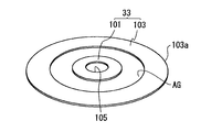
- the slow wave plate 33 having a structure separated into an inner and outer double is used.
- FIG. 3 is an external perspective view showing the arrangement of the slow wave plate 33
- FIG. 4 is a plan view of the slow wave plate 33
- FIG. 5 is a cross-sectional view of the main part showing the slow wave plate 33 provided on the planar antenna plate 31.
- the slow wave plate 33 includes a small-diameter member 101 disposed inside and a large-diameter member 103 surrounding the small-diameter member 101. Both the small diameter member 101 and the large diameter member 103 are flat plates formed in a ring shape.
- the small diameter member 101 and the large diameter member 103 may be formed of materials having the same dielectric constant, or may be formed of materials having different dielectric constants.
- An opening 105 penetrating in the thickness direction is provided at the center of the small diameter member 101 in order to be fixed to an inner conductor 41 (described later) passing through the center of the coaxial waveguide 37a. That is, the small diameter member 101 is fixed to the inner conductor 41 at the opening 105.
- the large diameter member 103 is fixed to, for example, the cover member 34 or the planar antenna plate 31 at the peripheral edge portion 103a.
- the small-diameter member 101 and the large-diameter member 103 are arranged with a space therebetween.
- An air layer (air gap AG) is interposed between the small diameter member 101 and the large diameter member 103.
- the dielectric of the region between the planar antenna plate 31 and the cover member 34 is made using the material of the small diameter member 101 and the large diameter member 103 and, if necessary, the air gap AG. Control the rate.
- Each of the small diameter member 101 and the large diameter member 103 is made of a dielectric material having a relative dielectric constant ⁇ exceeding 1.
- the relative dielectric constant ⁇ of the air gap AG which is an air layer is approximately 1.
- the small diameter member 101 and the large diameter member 103 are arranged,
- the dielectric constant in the region is non-uniform in a cross section parallel to the upper surface of the planar antenna plate 31.
- quartz having a relative dielectric constant ⁇ of 3.8 is used as the material of the small-diameter member 101 and the large-diameter member 103
- the dielectric constant in the upper region adjacent to the planar antenna plate 31 is the upper surface of the planar antenna plate 31.
- the interval between the small diameter member 101 and the large diameter member 103 (that is, the width L of the air gap AG) can be set to an arbitrary size.
- the width L of the air gap AG can be set smaller than that in FIG.
- the radial position where the air gap AG is provided can be variably adjusted. Even when the width L is the same, the ratio (area ratio and volume ratio) between the small diameter member 101 and the large diameter member 103 can be changed by changing the position where the air gap AG is provided.
- the distribution of the dielectric constant in the region between the planar antenna plate 31 and the cover member 34 can be easily changed. Can do.
- the small diameter member 101 and the large diameter member 103 in the slow wave plate 33 are not limited to an annular shape, and any shape can be adopted.
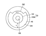
- FIG. 7 shows an example in which the large-diameter member 103 has an uneven shape.
- the inner periphery of the large-diameter member 103A is deformed so as to have a first arc portion CA1 and a second arc portion CA2 having a smaller radius of curvature than the first arc portion CA1.
- the width L of the air gap AG which is the distance between the small-diameter member 101 and the large-diameter member 103A, is not uniform and can be designed to be partially reduced only between the second arc CA2.
- illustration is omitted, the same configuration can be obtained by deforming the outer peripheral shape of the small diameter member 101 instead of the inner peripheral shape of the large diameter member 103.
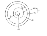
- the small-diameter member 101A is arranged eccentric from the center of the large-diameter member 103 (the same as the center of the planar antenna plate 31 or the center of the coaxial waveguide 37a).
- the width L of the air gap AG is set in the eccentric direction.
- the eccentric width can be partially reduced, and conversely, the side opposite to the eccentric direction can be designed to increase by the eccentric width. 7 and FIG.
- the asymmetric shape and the asymmetrical arrangement of the members constituting the slow wave plate 33 are such that the dielectric constant in both the radial direction and the circumferential direction on a plane parallel to the upper surface of the planar antenna plate 31. Can be made non-uniform. Therefore, for example, when the distribution of plasma in the processing container 1 has local strength and is biased, it is effective in correcting the bias. Furthermore, as shown in FIG. 9, the same configuration can be obtained by decentering the inner periphery of the large-diameter member 103.
- materials having different dielectric constants can be used as the material of the small diameter member 101 (101A) and the large diameter member 103 (103A).
- the planar antenna plate 31 is used in the case where quartz is used as the material of the small-diameter member 101 in FIGS. 3 to 5 and alumina (Al 2 O 3 ) having a relative dielectric constant ⁇ of 8.5 is used as the material of the large-diameter member 103.
- the planar antenna plate 31 is used.
- the distribution of the dielectric constant in the region between the planar antenna plate 31 and the cover member 34 can be easily changed. If the materials of the small diameter member 101 and the large diameter member 103 are different, the small diameter member 101 and the large diameter member 103 may be brought into contact with each other without providing the air gap AG unless damage is caused by thermal expansion or the like.
- the dielectric constant can be made non-uniform. In this case, it is preferable to select a material having the same thermal expansion coefficient between the small diameter member 101 and the large diameter member 103.
- a plurality of slow wave plates 33 are provided instead of a single slow wave plate, so that a region directly above the planar antenna plate 31 has a different dielectric constant. Can be subdivided into a plurality of small areas. Therefore, it is possible to finely control the adjustment of the wavelength of the microwave as compared with the case where a single slow wave plate is used, and the distribution of the plasma generated in the processing container 1 can be finely controlled.
- the members constituting the slow wave plate 33 are not limited to two members, the small diameter member 101 and the large diameter member 103, and three or more members may be used in combination.
- the thickness of the slow wave plate 33 is preferably set in consideration of the wavelength reduction due to the dielectric constant of the material constituting the slow wave plate 33 and the periodicity of the standing wave in the slow wave plate 33.
- a cover member 34 having a function of forming a waveguide is provided on the top of the processing container 1 so as to cover the planar antenna plate 31 and the slow wave plate 33.
- the cover member 34 is formed of a metal material such as aluminum, stainless steel, or copper.
- the upper end of the plate 13 and the cover member 34 are sealed by a sealing member 35 such as a spiral shield ring having conductivity so that microwaves do not leak outside.
- the cover member 34 is formed with a cooling water flow path 34a.
- the cover member 34, the slow wave plate 33, the planar antenna plate 31 and the transmission plate 28 can be cooled by allowing cooling water to flow through the cooling water flow path 34a. By this cooling mechanism, the cover member 34, the slow wave plate 33, the planar antenna plate 31, the transmission plate 28, and the plate 13 are prevented from being deformed or damaged by the heat of plasma.
- the plate 13, the planar antenna plate 31, and the cover member 34 are grounded.
- An opening 36 is formed at the center of the cover member 34, and the lower end of the waveguide 37 is connected to the opening 36.
- An electromagnetic wave generating device 39 that generates a microwave is connected to the other end side of the waveguide 37 via a matching circuit 38.
- the frequency of the microwave generated by the electromagnetic wave generator 39 for example, 2.45 GHz is preferably used, and 800 MHz to 1 GHz (preferably 800 MHz to 915 MHz), 8.35 GHz, 1.98 GHz, etc. can also be used.
- the waveguide 37 is connected to a coaxial waveguide 37a having a circular cross section extending upward from the opening 36 of the cover member 34, and an upper end portion of the coaxial waveguide 37a via a mode converter 40. And a rectangular waveguide 37b extending in the horizontal direction.
- the mode converter 40 has a function of converting the microwave propagating in the TE mode in the rectangular waveguide 37b into the TEM mode.
- An inner conductor 41 extends in the center of the coaxial waveguide 37a.
- the inner conductor 41 is connected and fixed to the center of the planar antenna plate 31 at its lower end. With such a structure, the microwave is efficiently and uniformly propagated radially and uniformly to the planar antenna plate 31 through the coaxial waveguide 37 a having the inner conductor 41.
- the microwave generated by the electromagnetic wave generator 39 is propagated to the planar antenna plate 31 through the waveguide 37 and further into the processing container 1 through the transmission plate 28. It has been introduced.
- the control unit 50 includes a process controller 51 including a CPU, and a user interface 52 and a storage unit 53 connected to the process controller 51.
- the process controller 51 controls each component (eg, the gas supply device 18, the exhaust device 24, the electromagnetic wave generation device 39, etc.) related to process conditions such as gas flow rate, pressure, and microwave output. It is a control means to control.
- the user interface 52 includes a keyboard on which a process manager manages command input to manage the plasma processing apparatus 100, a display for visualizing and displaying the operating status of the plasma processing apparatus 100, and the like.
- the storage unit 53 stores a recipe in which a control program (software) for realizing various processes executed by the plasma processing apparatus 100 under the control of the process controller 51 and processing condition data are recorded. Yes.
- recipes such as the control program and processing condition data may be stored in a computer-readable storage medium such as a CD-ROM, hard disk, flexible disk, flash memory, DVD, or Blu-ray disk. Alternatively, it may be transmitted from other devices as needed via, for example, a dedicated line and used online.
- the plasma processing apparatus 100 configured as described above, it is possible to perform damage-free plasma processing on the base film and the like. In addition, since the plasma processing apparatus 100 is excellent in plasma uniformity, process uniformity can be realized.
- a command is input from the user interface 52 to perform plasma nitridation processing in the plasma processing apparatus 100.
- the process controller 51 reads the recipe stored in the storage unit 53.
- a control signal is sent from the process controller 51 to each end device of the plasma processing apparatus 100 such as the gas supply device 18, the exhaust device 24, and the electromagnetic wave generator 39 so that the plasma nitridation process is executed under conditions based on the recipe.
- the gate valve 17 is opened and the wafer W is loaded into the processing chamber 1 through the loading / unloading port 16 and mounted on the mounting table 2.
- an inert gas and a nitrogen-containing gas are introduced from the gas supply device 18 into the processing container 1 through the gas introduction unit 15 at a predetermined flow rate. Further, the inside of the processing container 1 is adjusted to a predetermined pressure by adjusting the exhaust amount and the gas supply amount.
- the power of the electromagnetic wave generator 39 is turned on to generate microwaves.
- a microwave having a predetermined frequency, for example, 2.45 GHz is guided to the waveguide 37 through the matching circuit 38.
- the microwave guided to the waveguide 37 sequentially passes through the rectangular waveguide 37 b and the coaxial waveguide 37 a and is supplied to the planar antenna plate 31.
- the microwave propagates in the TE mode in the rectangular waveguide 37b, and the TE mode microwave is converted into the TEM mode by the mode converter 40, and the coaxial waveguide 37a is directed toward the planar antenna plate 31.
- Propagate The wavelength of the microwave is shortened by the slow wave plate 33 when propagating through the flat waveguide between the planar antenna plate 31 and the cover member 34.
- a small-diameter member 101, a large-diameter member 103, and a slow-wave plate 33 are used as the wave retardation plate 33 so that the dielectric constant of the flat waveguide is nonuniform in the radial direction of the planar antenna plate 31.
- It is composed of a double member having inner and outer members, and has a structure in which an air gap AG is interposed as required. As a result, the microwave passing through the flat waveguide can be controlled to a desired wavelength.
- the microwave whose wavelength has been shortened by the slow wave plate 33 enters the space above the wafer W in the processing chamber 1 from the microwave radiation hole 32, which is a hole formed through the planar antenna plate 31, through the transmission plate 28. Radiated.
- the microwave output is preferably in the range of 0.41 to 4.19 W / cm 2 as the power density per 1 cm 2 area of the planar antenna plate 31 from the viewpoint of efficiently supplying microwaves.
- the microwave output can be selected from a range of about 500 to 5000 W, for example, so that the power density is within the above range according to the purpose.
- An electromagnetic field is formed in the processing container 1 by the microwave radiated from the planar antenna plate 31 to the processing container 1 through the transmission plate 28.
- the inert gas and the nitrogen-containing gas are turned into plasma, respectively.
- the plasma excited by this microwave has a high density of 10 9 / cm 3 to 10 13 / cm 3 by radiating the microwave from a large number of microwave radiation holes 32 of the planar antenna plate 31 and the wafer. In the vicinity of W, the plasma has a low electron temperature of about 2 eV or less.
- the high-density plasma formed in this way has little plasma damage due to ions or the like on the underlying film.
- the silicon surface of the wafer W is nitrided by the action of active species such as radicals or ions in the plasma to form a thin silicon nitride film SiN.
- active species such as radicals or ions in the plasma
- silicon can be oxidized, and by using a film-forming raw material gas, a film can be formed by a plasma CVD method. It is also possible to perform etching using a gas.
- the slow wave plate 33 made of a dielectric has the dielectric constant in the region between the planar antenna plate 31 and the cover member 34 so that the planar antenna plate 31 has a dielectric constant. Since the cross section parallel to the upper surface of the substrate is configured to change in the radial direction and / or the circumferential direction, the wavelength of the microwave is controlled to control the plasma distribution in the processing chamber 1 without replacing the planar antenna plate 31. can do. Therefore, the plasma can be stably maintained in a desired distribution in the processing container 1. Even when the processing container 1 is increased in size in response to an increase in the size of the wafer W, the plasma distribution generated in the processing container 1 can be easily adjusted by changing the configuration of the slow wave plate 33.
- FIG. 11 is a plan view of the wave retardation plate 33 according to the second embodiment.
- the slow wave plate 33 includes a small-diameter member 101 disposed inside, a large-diameter member 103 surrounding the small-diameter member 101, and a plurality (eight in FIG. 11) disposed between the small-diameter member 101 and the large-diameter member 103.
- Each piece 107 is made of a dielectric.
- the piece 107 may be made of the same material as the small diameter member 101 and the large diameter member 103 or may be made of a different material. It is also possible to use a different material for each piece 107.
- the piece 107 is configured to be detachable from the slow wave plate 33, and one or a plurality of pieces 107 can be attached or detached.
- FIG. 11 shows a state where one piece 107 is removed.
- the portion becomes an air layer (air gap AG). Therefore, the distribution of the dielectric constant in the region between the planar antenna plate 31 and the cover member 34 can be easily changed by changing the number and arrangement of the pieces 107. That is, the dielectric constant in the region can be changed to be nonuniform in various patterns in the radial direction and the circumferential direction in a cross section parallel to the upper surface of the planar antenna plate 31.
- the pieces 107 are arranged in contact with the small diameter member 101 and / or the large diameter member 103, but may be separated from each other.
- the piece 107 is brought into contact with the small diameter member 101 and / or the large diameter member 103, it is preferable to select a material having the same thermal expansion coefficient as that of the small diameter member 101 and / or the large diameter member 103.
- an air layer air gap AG; not shown is interposed in the separated portion.
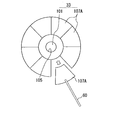
- FIG. 12 shows a mode in which the small-diameter member 101 and a plurality of detachable pieces 107A (eight in FIG. 12) are combined as a modified example of the slow wave plate 33 shown in FIG.
- a piece 107 ⁇ / b> A is disposed around the small diameter member 101 so as to surround the small diameter member 101.
- Each of the pieces 107A is made of a dielectric.
- the piece 107A may be made of the same material as the small diameter member 101 or may be made of a different material. It is also possible to use a different material for each piece 107A.
- the piece 107A is configured to be detachable using the arm 60, and one or a plurality of pieces 107A can be attached or detached.
- the portion becomes an air layer (air gap AG). Therefore, the distribution of the dielectric constant in the region between the planar antenna plate 31 and the cover member 34 can be easily changed by changing the number and arrangement of the pieces 107A. That is, the dielectric constant in the region can be changed to be nonuniform in various patterns in the radial direction and the circumferential direction in a cross section parallel to the upper surface of the planar antenna plate 31.
- the pieces 107A are arranged in contact with the small diameter member 101, but may be separated from each other.
- the piece 107A is brought into contact with the small diameter member 101, it is preferable to select a material having the same thermal expansion coefficient as that of the small diameter member 101.
- an air layer air gap AG; not shown
- the adjacent pieces 107A may be brought into contact with each other or separated from each other, and when they are brought into contact with each other, it is preferable to select a material having the same thermal expansion coefficient.
- an air layer air gap AG; not shown
- FIG. 13 shows a further modification of the present embodiment, which includes a base plate 111 and a plurality of detachable planar rectangular pieces 113 arranged in combination with the base plate 111.
- Both the base plate 111 and the piece 113 are made of a dielectric.
- the piece 113 may be made of the same material as the base plate 111 or may be made of a different material. It is also possible to use a different material for each piece 113.
- the base plate 111 is provided with a plurality of notches 111a, and an area between the planar antenna plate 31 and the cover member 34 is obtained by inserting or removing the piece 113 into or from the notches 111a.
- the distribution of the dielectric constant can be easily changed.
- an air layer air gap AG
- the dielectric is formed in the radial direction and the circumferential direction in a cross section parallel to the upper surface of the planar antenna plate 31. The rate becomes non-uniform.
- the dielectric constant is not uniform in the cross section parallel to the upper surface of the planar antenna plate 31 if the base plate 111 and the piece 113 are the same material. If the base plate 111 and the piece 113 are made of different materials, the dielectric constant becomes non-uniform in the radial direction and the circumferential direction in the cross section parallel to the upper surface of the planar antenna plate 31, and a dielectric constant distribution is generated. .
- FIG. 14 is a perspective view showing an external configuration of the slow wave plate 33 used in the third embodiment
- FIG. 15 is a cross-sectional view of the main part of the plasma processing apparatus showing a state where the slow wave plate 33 is attached. .
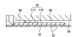
- the slow wave plate 33 includes a disk member 115 that is a flat plate having an area substantially the same as that of the planar antenna plate 31, and a ring-shaped member 117 that is disposed on the disk member 115.
- the ring-shaped member 117 is formed in a smaller area than the disk member 115.
- Both the disk member 115 and the ring-shaped member 117 are made of a dielectric.
- the disk member 115 and the ring-shaped member 117 may be made of the same material or different materials.
- the distribution of the dielectric constant in the region between the planar antenna plate 31 and the cover member 34 can be easily changed.
- the region immediately above the disk member 115 is an air layer (air gap AG) except for the portion where the ring-shaped member 117 having a predetermined dielectric constant exists, so that the dielectric constant is parallel to the upper surface of the planar antenna plate 31.
- the cross section is non-uniform.
- the ring-shaped member 117 is configured to be movable so that the arrangement can be changed by the arm 60 on the disk member 115. Since the shape of the air gap AG is changed by changing the arrangement of the ring-shaped member 117 ⁇ ⁇ , the dielectric constant distribution in the region between the planar antenna plate 31 and the cover member 34 is parallel to the upper surface of the planar antenna plate 31. It can be easily changed in a simple cross section.
- FIG. 16 is a cross-sectional view of the main part of the plasma processing apparatus 100 showing a state in which the slow wave plate 33 is attached.
- the ring-shaped member 117 is disposed in contact with the upper surface of the planar antenna plate 31, and the disk member 115 is stacked thereon.
- the ring-shaped member 115 is not movable but is fixed to the inner conductor 41 passing through the center of the coaxial waveguide 37a, for example.
- the ring-shaped member 117 is interposed between the disk member 115 and the planar antenna plate 31, so that the dielectric constant of the region between the planar antenna plate 31 and the cover member 34 is changed to the planar antenna plate 31. It is possible to make it non-uniform in a cross section parallel to the upper surface. That is, the region immediately below the disk member 115 is an air layer (air gap AG) except for a portion where the ring-shaped member 117 having a predetermined dielectric constant exists, and therefore, in a cross section parallel to the upper surface of the planar antenna plate 31. A dielectric constant distribution is generated.
- FIG. 17 is a cross-sectional view of a main part of the plasma processing apparatus showing a state where the slow wave plate 33 used in the fourth embodiment is attached.
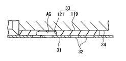
- the slow wave plate 33 of the present embodiment includes a base plate 119 and a recess, that is, a groove 121 partially formed in the base plate 119.
- one or more grooves 121 are partially formed on the upper surface of the base plate 119 (on the side opposite to the surface in contact with the planar antenna plate 31).
- the position, shape, depth, size, and the like of the groove 121 are not particularly limited.
- the groove 121 may be provided in an annular shape so as to surround the coaxial waveguide 37a, or a plurality of grooves 121 may be provided within the surface of the base plate 119. You may provide so that the groove
- the dielectric constant of the region between the planar antenna plate 31 and the cover member 34 is finely divided in a cross section parallel to the upper surface of the planar antenna plate 31. can do. That is, since the portion of the groove 121 ⁇ ⁇ becomes an air layer (air gap AG), a dielectric constant difference occurs between the base plate 119 having a predetermined dielectric constant. Therefore, the dielectric constant of the region between the planar antenna plate 31 and the cover member 34 can be made non-uniform in a cross section parallel to the upper surface of the planar antenna plate 31.
- a groove 121 may be partially provided on the lower surface of the base plate 119 (the surface in contact with the planar antenna plate 31).
- the grooves 121 may be partially provided on the upper and lower surfaces of the plate 119.
- the plasma processing apparatus of the present embodiment is the same as the plasma processing apparatus 100 (FIG. 1) of the first embodiment except that the configuration of the slow wave plate 33 is different. Only the configuration of the slow wave plate 33 will be described.
- 19 and 20 are plan views of the slow wave plate 33 according to the present embodiment.
- the slow wave plate 33 of the present embodiment has a single base plate 123 and one or a plurality of (9 in FIG. 19, one in FIG. 20) through-openings 125 penetrating in the thickness direction. .
- the shape, size, and arrangement position of the through-opening 125 in the base plate 123 are arbitrary and are not particularly limited. For example, a spiral shape, an annular shape, a semicircular shape, and an arc shape so as to surround the coaxial waveguide 37a. Etc. are preferably provided.
- the dielectric constant of the region between the planar antenna plate 31 and the cover member 34 is finely divided in a cross section parallel to the upper surface of the planar antenna plate 31. be able to. That is, since the portion of the through-opening 125 becomes an air layer (air gap AG), a dielectric constant difference occurs between the base plate 123 having a predetermined dielectric constant, and the dielectric constant is parallel to the upper surface of the planar antenna plate 31.
- the cross section can be non-uniform.
- the through openings 125 are non-uniformly arranged in the base plate 123, for example, the mounting position of the base plate 123 is arbitrary as shown by arrows in FIGS. By rotating at an angle of, it is possible to easily change the dielectric constant distribution in the region between the planar antenna plate 31 and the cover member 34.
- the finite element method is used to determine the effect of the structure of the slow wave plate 33 on the efficiency of introducing microwave power into the processing container 1. It was verified by 3D simulation. In the simulation, COMSOL (trade name; manufactured by COMSOL) was used as software, and the electric field strength and its distribution immediately below the transmission plate 28 were calculated when the following three types of slow wave plates were mounted.
- the material of the slow wave plate 33 is quartz.
- Slow wave plate A (example of the present invention): In a double wave structure slow wave plate similar to that shown in FIGS. 3 to 5, the radial distance from the center to the outer periphery of the small diameter member 101 is about 160 mm.
- the width of the air gap AG was set to 10 mm, 20 mm, 30 mm, 40 mm, 50 mm, 60 mm, and 72.5 mm.
- Slow wave plate B (example of the present invention): In a slow wave plate having a double ring structure similar to that shown in FIGS. 3 to 5, the radial distance from the center to the outer peripheral portion of the small diameter member 101 is about 195 mm.
- the width of the air gap AG was set to 10 mm, 20 mm, 30 mm, and 38.5 mm, respectively.
- Slow wave plate S (comparative example): A single disk shape.
- FIG. 21 shows the electric field intensity distribution immediately below the transmission plate 28 in black and white.
- the white area has a high electric field intensity and the black area has a low electric field intensity.
- the electric field distribution in the processing container 1 can be greatly changed.
- the width L of the air gap AG when the width L of the air gap AG is 30 mm, the electric field distribution is strong immediately below the peripheral portion of the transmission plate 28, and when the width L is 40 mm, the electric field distribution is strong immediately below the center portion of the transmission plate 28.
- the tendency of the electric field distribution to change depending on the width L of the air gap AG was recognized.
- the electric field distribution is biased such that the electric field is strengthened only in a portion where the electric field distribution is locally weak in the processing container 1. It is thought that control that positively corrects is possible.
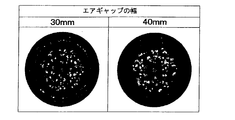
- a plasma nitriding process was performed on the silicon wafer using a plasma processing apparatus having the same configuration as the plasma processing apparatus 100 shown in FIG.
- a plasma processing apparatus having the same configuration as the plasma processing apparatus 100 shown in FIG.
- the retardation plate 33 a retardation plate having a double ring structure similar to that shown in FIGS. 3 to 5 was used.
- the width of the air gap AG was 30 mm or 40 mm.
- the process conditions are as follows.
- FIG. 22 shows the electric field intensity distribution immediately below the transmission plate 28 in the simulation experiment in black and white.
- the white area has a high electric field strength
- the black area has a low electric field intensity.
- the plasma processing apparatus 100 of the present invention can be applied to, for example, a plasma oxidation processing apparatus, a plasma CVD processing apparatus, a plasma etching processing apparatus, a plasma ashing processing apparatus, etc. in addition to a plasma nitriding processing apparatus.
- the plasma processing apparatus 100 including the planar antenna plate 31 according to the present invention is not limited to processing a semiconductor wafer as an object to be processed.
- a flat panel display apparatus such as a liquid crystal display apparatus or an organic EL display apparatus
- the present invention can also be applied to a plasma processing apparatus using a substrate of a battery panel as an object to be processed.
Landscapes
- Physics & Mathematics (AREA)
- Engineering & Computer Science (AREA)
- Plasma & Fusion (AREA)
- Chemical & Material Sciences (AREA)
- Analytical Chemistry (AREA)
- Electromagnetism (AREA)
- Spectroscopy & Molecular Physics (AREA)
- Plasma Technology (AREA)
- Drying Of Semiconductors (AREA)
- Chemical Vapour Deposition (AREA)
Abstract
Description
誘電体によって構成されるとともに、前記平面アンテナ部材と、前記平面アンテナ部材を上方から覆うカバー部材との間の領域の誘電率が、前記平面アンテナ部材の上面と平行な断面において、非均一である。
以下、本発明の実施の形態について図面を参照して詳細に説明する。図1は、本発明の第1の実施の形態に係るプラズマ処理装置100の構成例を模式的に示す断面図である。図2は、図1のプラズマ処理装置100に用いられる平面アンテナを示す平面図である。プラズマ処理装置100は、複数のスロット状の孔を有する平面アンテナ、特にRLSA(Radial Line Slot Antenna;ラジアルラインスロットアンテナ)にて処理容器内にマイクロ波を導入してプラズマを発生させることにより、高密度かつ低電子温度のプラズマを発生させ得るプラズマ処理装置として構成されている。プラズマ処理装置100では、109/cm3~1013/cm3のプラズマ密度で、かつ2eV 以下の低電子温度を有するプラズマによる処理が可能である。従って、プラズマ処理装置100は、各種半導体装置の製造過程において好適に利用できるものである。
次に、図11から図13を参照しながら、本発明の第2の実施の形態に係るプラズマ処理装置について説明する。本実施の形態のプラズマ処理装置は、遅波板33の構成が異なる点以外は、第1の実施の形態のプラズマ処理装置100(図1)と同じであるため、全体の説明は省略し、遅波板33の構成についてのみ説明を行う。図11は、第2の実施の形態に係る遅波板33の平面図である。遅波板33は、内側に配置される小径部材101と、小径部材101を囲む大径部材103と、小径部材101と大径部材103との間に介在配置された複数(図11では8個)の着脱自在なピース107を有している。ピース107は、いずれも誘電体から構成されている。ピース107は、小径部材101及び大径部材103と同じ材質でもよいし、異なる材質でもよい。また、ピース107毎に異なる材質を用いることも可能である。
次に、図14から図16を参照しながら、本発明の第3の実施の形態に係るプラズマ処理装置について説明する。本実施の形態のプラズマ処理装置は、遅波板33の構成が異なる点以外は、第1の実施の形態のプラズマ処理装置100(図1)と同じであるため、全体の説明は省略し、遅波板33の構成についてのみ説明を行う。図14は、第3の実施の形態に用いる遅波板33の外観構成を示す斜視図であり、図15は、遅波板33を取り付けた状態を示すプラズマ処理装置の要部断面図である。遅波板33は、平面アンテナ板31と略同程度の面積の平板である円盤部材115と、該円盤部材115の上に重ねて配置されたリング状部材117と、を有している。リング状部材117は、円盤部材115よりも小面積に形成されている。円盤部材115 とリング状部材117 は、いずれも誘電体から構成されている。円盤部材115 とリング状部材117 とは、同じ材質でもよいし、異なる材質でもよい。
次に、図17及び図18を参照しながら、本発明の第4の実施の形態に係るプラズマ処理装置について説明する。本実施の形態のプラズマ処理装置は、遅波板33の構成が異なる点以外は、第1の実施の形態のプラズマ処理装置100(図1)と同じであるため、全体の説明は省略し、遅波板33の構成についてのみ説明を行う。図17は、第4の実施の形態に用いる遅波板33を取り付けた状態を示すプラズマ処理装置の要部断面図である。本実施の形態の遅波板33は、ベース板119と、このベース板119に部分的に形成された凹部、すなわち溝121とを有している。つまり、ベース板119の上面(平面アンテナ板31に接する面とは反対側)には、部分的に一つないし複数の溝121が形成されている。溝121の配設位置や形状、深さや大きさなどは特に限定されるものではなく、例えば同軸導波管37aを囲むように環状に設けてもよいし、ベース板119の面内に複数の溝121が点在するように設けてもよい。
次に、図19及び図20を参照しながら、本発明の第5の実施の形態に係るプラズマ処理装置について説明する。本実施の形態のプラズマ処理装置は、遅波板33の構成が異なる点以外は、第1の実施の形態のプラズマ処理装置100(図1)と同じであるため、全体の説明は省略し、遅波板33の構成についてのみ説明を行う。図19及び図20は、本実施の形態に係る遅波板33の平面図である。本実施の形態の遅波板33は、単体のベース板123と、その厚み方向に貫通する一つ又は複数(図19では9つ、図20では1つ)の貫通開口125を有している。ベース板123における貫通開口125形状や大きさ、配設位置は任意であり、特に限定されるものではないが、例えば同軸導波管37aを囲むように螺旋状、環状、半円状、円弧状等に設けることが好ましい。

N2ガス/Arガスの体積流量比:20%、
流量:200mL/min(sccm)、
プロセス圧力:20Pa、
マイクロ波出力:1500W、
載置台温度:500℃、
処理時間:90秒

Claims (12)
- 被処理体に対してプラズマ処理するプラズマ処理装置であって、
被処理体を収容する真空引き可能な処理容器と、
電磁波発生装置で発生した電磁波を前記処理容器内に導入する平面アンテナ部材と、
前記電磁波を前記平面アンテナ部材へ供給する導波管と、
前記平面アンテナ部材の上に重ねて設けられ、前記導波管から供給された前記電磁波の波長を変化させる遅波板と、
前記遅波板及び前記平面アンテナ部材を上方から覆うカバー部材と、を備え、
前記遅波板は、誘電体によって構成されるとともに、前記平面アンテナ部材と前記カバー部材との間の領域の誘電率が、前記平面アンテナ部材の上面と平行な断面において、非均一である。 - 請求項1に記載のプラズマ処理装置において、
前記遅波板が、誘電率が同じ又は異なる複数の部材を組み合わせて形成されている。 - 請求項2に記載のプラズマ処理装置において、
前記複数の部材の間に空気層が介在している。 - 請求項2に記載のプラズマ処理装置において、
前記複数の部材の一部が取り外し可能である。 - 請求項2に記載のプラズマ処理装置において、
前記複数の部材の配置位置が可変である。 - 請求項1に記載のプラズマ処理装置において、
前記遅波板が、第1の部材と、該第1の部材よりも大きな第2の部材と、を含み、
前記第1の部材の周囲に前記第2の部材が配置され、前記第1の部材と前記第2の部材との間に空気層が介在している。 - 請求項1に記載のプラズマ処理装置において、
前記遅波板が、第1の部材と、該第1の部材よりも大きな第2の部材と、を含み、
前記第1の部材と前記第2の部材がこれらの厚み方向に重ねて配置されている。 - 請求項7に記載のプラズマ処理装置において、
前記第1
の部材が前記平面アンテナ部材に接触して配置され、前記第2の部材が前記第1の部材上に重ねて配置されている。 - 請求項7に記載のプラズマ処理装置において、
前記第2の部材が前記平面アンテナ部材に接触して配置され、前記第1の部材が前記第2の部材上に重ねて配置されている。 - 請求項1に記載のプラズマ処理装置において、
前記遅波板が平板形状をなし、その厚み方向に複数の凹部を有しており、該凹部に空気層が介在している。 - 請求項1に記載のプラズマ処理装置において、
前記遅波板が平板形状をなし、その厚み方向に複数の貫通開口部を有しており、該貫通開口部に空気層が介在している。 - プラズマ処理装置の平面アンテナ部材の上に重ねて設けられ、導波管から供給された電磁波の波長を変化させる遅波板であって、
前記遅波板は、誘電体によって構成されるとともに、
前記平面アンテナ部材と、前記平面アンテナ部材を上方から覆うカバー部材との間の領域の前記遅波板の誘電率が、前記平面アンテナ部材の上面と平行な断面において、非均一である。
Priority Applications (4)
| Application Number | Priority Date | Filing Date | Title |
|---|---|---|---|
| KR1020147002619A KR101411085B1 (ko) | 2009-09-30 | 2010-09-29 | 플라즈마 처리 장치 |
| US13/498,339 US20120180953A1 (en) | 2009-09-30 | 2010-09-29 | Plasma processing apparatus and wave retardation plate used therein |
| KR1020147002620A KR101411171B1 (ko) | 2009-09-30 | 2010-09-29 | 플라즈마 처리 장치 |
| CN2010800168680A CN102396053A (zh) | 2009-09-30 | 2010-09-29 | 等离子体处理装置及其使用的滞波板 |
Applications Claiming Priority (2)
| Application Number | Priority Date | Filing Date | Title |
|---|---|---|---|
| JP2009225984A JP5479013B2 (ja) | 2009-09-30 | 2009-09-30 | プラズマ処理装置及びこれに用いる遅波板 |
| JP2009-225984 | 2009-09-30 |
Publications (1)
| Publication Number | Publication Date |
|---|---|
| WO2011040465A1 true WO2011040465A1 (ja) | 2011-04-07 |
Family
ID=43826280
Family Applications (1)
| Application Number | Title | Priority Date | Filing Date |
|---|---|---|---|
| PCT/JP2010/066946 Ceased WO2011040465A1 (ja) | 2009-09-30 | 2010-09-29 | プラズマ処理装置及びこれに用いる遅波板 |
Country Status (5)
| Country | Link |
|---|---|
| US (1) | US20120180953A1 (ja) |
| JP (1) | JP5479013B2 (ja) |
| KR (3) | KR101411171B1 (ja) |
| CN (1) | CN102396053A (ja) |
| WO (1) | WO2011040465A1 (ja) |
Families Citing this family (8)
| Publication number | Priority date | Publication date | Assignee | Title |
|---|---|---|---|---|
| JP5805227B2 (ja) | 2014-01-28 | 2015-11-04 | 東京エレクトロン株式会社 | プラズマ処理装置 |
| JP6478748B2 (ja) * | 2015-03-24 | 2019-03-06 | 東京エレクトロン株式会社 | マイクロ波プラズマ源およびプラズマ処理装置 |
| KR102487342B1 (ko) | 2016-06-14 | 2023-01-13 | 삼성전자주식회사 | 정전척 어셈블리 및 이를 구비하는 플라즈마 처리장치 |
| US12159768B2 (en) | 2019-03-25 | 2024-12-03 | Recarbon, Inc. | Controlling exhaust gas pressure of a plasma reactor for plasma stability |
| CN110311223B (zh) * | 2019-07-25 | 2021-09-24 | 哈尔滨工业大学 | 信号增强型等离子体隐身天线窗 |
| JP7300957B2 (ja) * | 2019-10-08 | 2023-06-30 | 東京エレクトロン株式会社 | プラズマ処理装置及び天壁 |
| JP7772325B2 (ja) * | 2022-06-09 | 2025-11-18 | 東京エレクトロン株式会社 | プラズマ処理装置及び共振周波数測定方法 |
| TW202514705A (zh) | 2023-05-30 | 2025-04-01 | 荷蘭商Asm Ip私人控股有限公司 | 用於將能量提供至具有多個功率信號輸入之電漿腔室的系統以及半導體處理系統 |
Citations (2)
| Publication number | Priority date | Publication date | Assignee | Title |
|---|---|---|---|---|
| JP2002093788A (ja) * | 2000-07-11 | 2002-03-29 | Tokyo Electron Ltd | プラズマ処理装置 |
| JP2002231637A (ja) * | 2001-01-30 | 2002-08-16 | Nihon Koshuha Co Ltd | プラズマ処理装置 |
Family Cites Families (5)
| Publication number | Priority date | Publication date | Assignee | Title |
|---|---|---|---|---|
| JP4747404B2 (ja) * | 2000-09-04 | 2011-08-17 | 東京エレクトロン株式会社 | プラズマ処理装置 |
| JP4727057B2 (ja) * | 2001-03-28 | 2011-07-20 | 忠弘 大見 | プラズマ処理装置 |
| JP4677918B2 (ja) * | 2006-02-09 | 2011-04-27 | 東京エレクトロン株式会社 | プラズマ処理装置及びプラズマ処理方法 |
| JP2007335346A (ja) * | 2006-06-19 | 2007-12-27 | Tokyo Electron Ltd | マイクロ波導入装置及びプラズマ処理装置 |
| TWI393488B (zh) * | 2007-10-04 | 2013-04-11 | Tokyo Electron Ltd | 電漿處理裝置及電漿密度分布之調整方法 |
-
2009
- 2009-09-30 JP JP2009225984A patent/JP5479013B2/ja active Active
-
2010
- 2010-09-29 CN CN2010800168680A patent/CN102396053A/zh active Pending
- 2010-09-29 US US13/498,339 patent/US20120180953A1/en not_active Abandoned
- 2010-09-29 WO PCT/JP2010/066946 patent/WO2011040465A1/ja not_active Ceased
- 2010-09-29 KR KR1020147002620A patent/KR101411171B1/ko active Active
- 2010-09-29 KR KR1020127011200A patent/KR20120062923A/ko not_active Ceased
- 2010-09-29 KR KR1020147002619A patent/KR101411085B1/ko active Active
Patent Citations (2)
| Publication number | Priority date | Publication date | Assignee | Title |
|---|---|---|---|---|
| JP2002093788A (ja) * | 2000-07-11 | 2002-03-29 | Tokyo Electron Ltd | プラズマ処理装置 |
| JP2002231637A (ja) * | 2001-01-30 | 2002-08-16 | Nihon Koshuha Co Ltd | プラズマ処理装置 |
Also Published As
| Publication number | Publication date |
|---|---|
| JP5479013B2 (ja) | 2014-04-23 |
| US20120180953A1 (en) | 2012-07-19 |
| KR101411085B1 (ko) | 2014-06-25 |
| KR20120062923A (ko) | 2012-06-14 |
| CN102396053A (zh) | 2012-03-28 |
| KR20140019880A (ko) | 2014-02-17 |
| KR101411171B1 (ko) | 2014-06-23 |
| JP2011077228A (ja) | 2011-04-14 |
| KR20140019879A (ko) | 2014-02-17 |
Similar Documents
| Publication | Publication Date | Title |
|---|---|---|
| JP5893865B2 (ja) | プラズマ処理装置およびマイクロ波導入装置 | |
| KR101317018B1 (ko) | 플라즈마 처리 장치 | |
| JP5479013B2 (ja) | プラズマ処理装置及びこれに用いる遅波板 | |
| JP2010087184A (ja) | プラズマ処理装置 | |
| JP5096047B2 (ja) | マイクロ波プラズマ処理装置およびマイクロ波透過板 | |
| JP2011199003A (ja) | シリコン酸化膜の形成方法、及びプラズマ処理装置 | |
| JP2007042951A (ja) | プラズマ処理装置 | |
| JP4979389B2 (ja) | プラズマ処理装置 | |
| JP2006244891A (ja) | マイクロ波プラズマ処理装置 | |
| JP2010232493A (ja) | プラズマ処理装置 | |
| JP5860392B2 (ja) | プラズマ窒化処理方法及びプラズマ窒化処理装置 | |
| JP2013045551A (ja) | プラズマ処理装置、マイクロ波導入装置及びプラズマ処理方法 | |
| US20100307685A1 (en) | Microwave plasma processing apparatus | |
| CN101849444B (zh) | 平板天线部件以及具备其的等离子体处理装置 | |
| WO2011013633A1 (ja) | 平面アンテナ部材およびこれを備えたプラズマ処理装置 | |
| JP5728565B2 (ja) | プラズマ処理装置及びこれに用いる遅波板 | |
| KR20120112244A (ko) | 플라즈마 질화 처리 방법, 플라즈마 질화 처리 장치 및 반도체 장치의 제조 방법 | |
| WO2011007745A1 (ja) | マイクロ波プラズマ処理装置およびマイクロ波プラズマ処理方法 | |
| JP2013033979A (ja) | マイクロ波プラズマ処理装置 | |
| JP5066502B2 (ja) | プラズマ処理装置 | |
| JP2011029250A (ja) | マイクロ波プラズマ処理装置およびマイクロ波プラズマ処理方法 | |
| JP2009099975A (ja) | プラズマ処理装置 |
Legal Events
| Date | Code | Title | Description |
|---|---|---|---|
| WWE | Wipo information: entry into national phase |
Ref document number: 201080016868.0 Country of ref document: CN |
|
| 121 | Ep: the epo has been informed by wipo that ep was designated in this application |
Ref document number: 10820580 Country of ref document: EP Kind code of ref document: A1 |
|
| WWE | Wipo information: entry into national phase |
Ref document number: 13498339 Country of ref document: US |
|
| NENP | Non-entry into the national phase |
Ref country code: DE |
|
| ENP | Entry into the national phase |
Ref document number: 20127011200 Country of ref document: KR Kind code of ref document: A |
|
| 122 | Ep: pct application non-entry in european phase |
Ref document number: 10820580 Country of ref document: EP Kind code of ref document: A1 |