WO2010117034A1 - プローブカード - Google Patents
プローブカード Download PDFInfo
- Publication number
- WO2010117034A1 WO2010117034A1 PCT/JP2010/056361 JP2010056361W WO2010117034A1 WO 2010117034 A1 WO2010117034 A1 WO 2010117034A1 JP 2010056361 W JP2010056361 W JP 2010056361W WO 2010117034 A1 WO2010117034 A1 WO 2010117034A1
- Authority
- WO
- WIPO (PCT)
- Prior art keywords
- probe
- probe card
- beam portion
- shape
- wiring board
- Prior art date
- Legal status (The legal status is an assumption and is not a legal conclusion. Google has not performed a legal analysis and makes no representation as to the accuracy of the status listed.)
- Ceased
Links
Images






Classifications
-
- G—PHYSICS
- G01—MEASURING; TESTING
- G01R—MEASURING ELECTRIC VARIABLES; MEASURING MAGNETIC VARIABLES
- G01R1/00—Details of instruments or arrangements of the types included in groups G01R5/00 - G01R13/00 and G01R31/00
- G01R1/02—General constructional details
- G01R1/06—Measuring leads; Measuring probes
- G01R1/067—Measuring probes
- G01R1/06711—Probe needles; Cantilever beams; "Bump" contacts; Replaceable probe pins
- G01R1/06716—Elastic
-
- G—PHYSICS
- G01—MEASURING; TESTING
- G01R—MEASURING ELECTRIC VARIABLES; MEASURING MAGNETIC VARIABLES
- G01R1/00—Details of instruments or arrangements of the types included in groups G01R5/00 - G01R13/00 and G01R31/00
- G01R1/02—General constructional details
- G01R1/06—Measuring leads; Measuring probes
- G01R1/067—Measuring probes
- G01R1/06711—Probe needles; Cantilever beams; "Bump" contacts; Replaceable probe pins
- G01R1/06733—Geometry aspects
Definitions
- the present invention relates to a probe card, and more particularly to a probe card that can be suitably used for a probe card in which probes extending in the vertical direction are arranged in an array.
- probes also referred to as contacts
- vertical type probes the advantage of the vertical probe is that it can be arranged in an array (see Patent Document 1).
- the present invention has been made in view of these points, and while keeping the load applied to the probe low, the probe stroke length is increased in a narrow effective space, and the probe is stably expanded and contracted. It is an object of the present invention to provide a probe card that can be used.
- the probe card of the present invention includes, as a first aspect, a wiring board having connection terminals and a first beam portion to an nth beam formed in a plate shape having a predetermined width.
- a plurality of beam portions up to a portion are arranged in an inclined manner or horizontally, and from a first beam portion connected directly or indirectly to a connection terminal of a wiring board
- the stroke length of the probe can be reduced in a narrow effective space. Can be long.
- each beam part which comprises the spring part of a probe is each formed in the plate shape which has predetermined width
- the probe card according to the second aspect of the present invention is the probe card according to the first aspect, wherein the beam part has a polygonal plate, a circular plate, an elliptical plate or other one or both ends narrower than the width of the intermediate portion. It is characterized by being formed in a plate shape.
- the elastic force can be made larger than that of the probe having each beam portion formed in a linear shape. Further, the elastic force of the probe can be easily controlled by changing the width of the beam portion.
- the probe card according to the third aspect of the present invention is characterized in that, in the probe card according to the second aspect, the beam portion is formed in a donut shape.
- the control of the elastic force of the probe can be facilitated by the size of the hole provided in each beam portion.
- the probe card according to the fourth aspect of the present invention is the probe card according to the first aspect, wherein the contact portion of the beam portion that contacts the electrode pad to be contacted as the contact portion of the probe is formed in parallel with the electrode pad. It is characterized by being.
- the contact area with the electrode pad can be increased.
- the probe card according to a fifth aspect of the present invention is the probe card according to the first aspect, wherein the probe is arranged between the connection terminal of the wiring board and the first beam part by arranging the first beam part from the wiring board on the electrode pad. It is characterized by having a raised base that is raised on the installation side.
- the probe card of the fifth aspect of the present invention it is possible to suppress the first inclined beam portion from bottoming on the wiring board.
- a probe card according to a sixth aspect of the present invention is the probe card according to the fifth aspect, wherein the probe is formed to extend in a horizontal direction from the bulkhead, and the bulkhead and the lower end of the first beam portion are connected to each other. It has a horizontal beam part to be connected.
- the probe card of the sixth aspect of the present invention since the horizontal beam portion is interposed between the bulkhead and the first inclined beam portion, the behavior control of the elastic deformation of the probe can be easily performed.
- a probe card according to a seventh aspect of the present invention is the probe card according to the first aspect, wherein the probe is connected between the ends of the beam portions adjacent in the vertical direction and is formed in a column shape. It is characterized by having a vertical connection part.
- the probe card of the seventh aspect of the present invention it is possible to prevent interfacial peeling from each beam part by interposing the vertical connection part between each beam part.
- the shape of the beam portion constituting the spring portion of the probe, the stepped shape thereof, and the like are as described above, the load applied to the probe is kept low while the effective space is small.
- the effect is that the stroke length of the probe is increased and the probe can stably extend and contract.
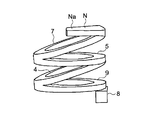
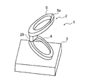
- the perspective view which shows an example of the probe card of this embodiment The perspective view which shows an example of the probe card of this embodiment
- the perspective view which shows an example of the probe of this embodiment The perspective view which shows an example of the probe of this embodiment
- the perspective view which shows an example of the probe of this embodiment The perspective view which shows an example of the state which formed the vertical connection part in the probe of this embodiment
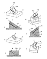
- Sectional drawing which shows an example of the formation process of the bulkhead and horizontal beam part in the manufacturing method of the probe of this embodiment
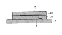
- Sectional drawing which shows an example of the joining method of a bulkhead base, a horizontal beam part, and a 1st inclination beam part in the manufacturing method of the probe of this embodiment.
- Sectional drawing which shows an example of the joining method of a 1st inclination beam part, a vertical connection part, and a 2nd inclination beam part in the manufacturing method of the probe of this embodiment.
- a perspective view showing an example of another probe A perspective view showing an example of another probe The perspective view which shows an example of the probe of other embodiment
- probe card of the present invention will be described based on an embodiment thereof.
- the probe card 1 includes a wiring board 3 having a connection terminal 3a and a probe 2 as shown in FIG.
- the probe 2 of this embodiment has a spring portion composed of a plurality of beam portions (for example, 4, 5, etc.).
- this spring portion as shown in FIG. 1 or FIG. 2, the first beam portion 4 to the nth beam portion (n is an arbitrary integer equal to or greater than 2) (part number is 5, 6, or N)
- n is an arbitrary integer equal to or greater than 2
- a plurality of beam portions up to a certain number are arranged in an inclined manner or horizontally.
- the inclined beam portion is called a second inclined beam portion 5
- the horizontally arranged beam portion is called a second horizontal beam portion 6 as shown in FIG. 3, for example.
- this spring portion is used as each hinge portion H (see FIG.
- a single arm pantograph shape is formed.
- This spring part may be formed in a Z shape as shown in FIG. 3 or FIG.
- the single arm pantograph shape or Z-shape of the spring portion may be single as shown in FIG. 1 or FIG. 3, or may be continuous as shown in FIG. 2 or FIG.
- the beam portions are each formed in a plate shape having a predetermined width.
- the beam portion (for example, 4) is preferably formed in a plate shape in which the width of one end or both ends of a polygonal plate, a circular plate, an elliptical plate or the like is narrower than the width of the intermediate portion. Further, it is more preferable that the beam portion (for example, 4) is formed in a donut shape.
- the contact portion (for example, 5a, 6a, Na) of the beam portion is in contact with an electrode pad (not shown) to be contacted as a contact portion of the probe 2 as shown in FIG.
- the contact portion (for example, 5a, 6a, Na) of the beam portion is preferably formed in parallel with the electrode pad.
- the first inclined beam portion 4 may be directly connected to the connection terminal 3a of the wiring board 3 or may be indirectly connected.
- the probe 2 may have a metal bulkhead 8 between the connection terminal 3 a of the wiring board 3 and the first beam portion 4.
- the raised base 8 raises the first beam portion 4 from the wiring board 3 to the electrode pad arrangement side (upward), and indirectly connects the first inclined beam portion 4 and the connection terminal 3 a of the wiring board 3. Connect.
- the probe 2 may have a horizontal beam portion 9 as shown in FIG. 3 or FIG.
- the horizontal beam portion 9 is formed to extend in the horizontal direction from the bulkhead 8 and connects the bulkhead 8 and the lower end of the first beam portion 4.
- the probe 2 may have a vertical connection portion 25 as shown in FIG.
- the vertical connection portion 25 is formed in a columnar shape, and between each end portion of each beam portion adjacent in the vertical direction, for example, the upper end of the first inclined beam portion 4 and the second beam portion 5 (or 6). It is interposed between the lower end.
- the probe 2 of the probe card 1 of this embodiment can be formed by various methods.
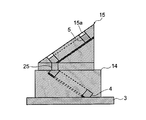
- a first resist plating mold is formed in which the first inclined beam portion 4 is formed in the hole 10a as shown in FIG. 6A.
- the first inclined beam portion 4 is formed by plating
- the first resist plating mold is removed as shown in FIG. 6C
- the first resist embedding base having a flat upper surface as shown in FIG. 6D is formed, as shown in FIG. 6E.
- Formation of a second resist plating mold in which the second inclined beam portion 5 is formed by plating inside the hole 15a, plating formation of the second beam portion 5 (or 6) as shown in FIG. 6F, and resist as shown in FIG. 6G It is formed through removal.
- the probe 2 of this embodiment is an optional additional process.
- the resist plating mold 21 for the horizontal beam portion 9 and the horizontal beam portion 9 plating are formed and the vertical connection portion 25 as shown in FIG. 10 is formed. May be.
- the spring portion of the probe 2 is independent (or continuous as shown in FIG. 2) by arranging a plurality of beam portions 4 and 5 vertically as shown in FIG.
- the single arm pantograph shape (or the Z shape shown in FIG. 3 or 4) is formed. Therefore, the stroke length of the probe 2 can be increased in a narrow effective space.
- Each of the aforementioned beam portions (for example, 4 and 5) is formed in a plate shape having a predetermined width. Therefore, unlike the probe 2 formed by combining linear or C-shaped beam portions (for example, 4 and 5) as shown in FIG. 11 or FIG. 12, the probe 2 moves unnecessarily in the horizontal direction when the probe 2 contracts. Therefore, it is possible to prevent the behavior of the expansion / contraction operation of the probe from being disturbed.
- the beam portion is preferably formed in a plate shape in which the width of one end or both ends of a polygonal plate, a circular plate, an elliptical plate or the like is narrower than the width of the intermediate portion.
- the elastic force can be made larger than that of the probe 2 having a narrow linear or C-shaped beam portion (for example, 4, 5) as shown in FIG.
- the control of the elastic force of the probe 2 such that the elastic force is increased in accordance with the contraction amount of the spring part of the probe 2 by making the width of the intermediate part of the beam part larger than the widths of the upper and lower ends. can do.
- the beam portion is formed in a donut shape. This makes it easy to adjust the elastic force of the probe 2 caused by the low load applied to the probe 2 in the decreasing direction depending on the size of the hole provided in each beam portion. Even if it is increased, the elastic force generated by the probe 2 can be reduced. As a result, it is possible to improve the behavioral stability of the probe 2 in the contraction direction by enlarging the entire width of the probe 2 and to easily control the elastic force of the probe 2.
- the contact portion (for example, 5a, 6a, Na) of the beam portion is preferably formed in parallel with the electrode pad. Thereby, a contact area with an electrode pad can be enlarged.
- the probe 2 preferably has a bulkhead 8 as shown in FIG. 2 or FIG.
- a bulkhead 8 By forming the bulkhead 8, it is possible to prevent the first inclined beam portion 4 from bottoming out to the wiring board 3 at an early stage.
- the probe 2 is preferably formed with a horizontal beam portion 9. Even if the horizontal beam portion 9 is deformed, the position of the contact portion (for example, 5a, 6a, Na) of the beam portion is less likely to be shifted left and right, so that the elastic force of the probe 2 is controlled by adding the horizontal beam portion 9, The behavior control of the elastic deformation of the probe 2 can be easily performed.
- the probe 2 has a vertical connection portion 25 as shown in FIG.
- the vertical connection portion 25 By interposing the vertical connection portion 25 between the beam portions (for example, 4 and 5), it is possible to prevent interface peeling from between the beam portions (for example, 4 and 5).
- the shape of the beam portion constituting the spring portion of the probe 2 and their columnar shape are as described above, the load applied to the probe 2 is kept low.
- the effect is that the stroke length of the probe 2 can be increased in a narrow effective space, and the probe 2 can be stably expanded and contracted.
Landscapes
- Physics & Mathematics (AREA)
- General Physics & Mathematics (AREA)
- Measuring Leads Or Probes (AREA)
- Testing Or Measuring Of Semiconductors Or The Like (AREA)
- Testing Of Individual Semiconductor Devices (AREA)
Abstract
【課題】プローブに加える荷重を低く維持したまま、狭小の有効スペースでプローブのストローク長さを長くし、かつ、プローブが安定して伸縮動作することができるプローブカードを提供する。 【解決手段】本発明のプローブカード1のプローブ2においては、ばね部として、ドーナツ形状の楕円板状に形成された第1ビーム部4および第2ビーム部5が傾斜配置されている。また、プローブ2は、第1ビーム部4の上端部および第2ビーム部5の下端部をヒンジ部Hとして2個のビーム部を連結させ、シングルアームパンタグラフ形状に形成されている。
Description
本発明は、プローブカードに係り、特に、垂直方向に延在するプローブがアレイ配置されるプローブカードに好適に利用できるプローブカードに関する。
一般的に、プローブカードに用いられるプローブ(接触子とも言う。)については、主に、水平カンチレバー型プローブと、垂直型プローブとの2種類のプローブが挙げられる。そのうちの垂直型プローブのメリットは、アレイ配置できる点である(特許文献1を参照)。
従来の垂直型プローブにおいては、プローブの高い耐久性と低い接点抵抗とを実現するため、低荷重と高ストロークとの両立が要求されていた。
しかしながら、従来の垂直型プローブにおいては、最近のプローブの狭小化により各プローブ間のピッチ間距離およびプローブの有効スペースが小さくなったため、プローブに加える荷重を低く維持したまま、狭小の有効スペースでプローブのストローク長さを長くすることが難しくなってきたという問題が生じてきた。
したがって、例えば数μm~数十μm幅のプローブを150μm以下のピッチ間隔で配置する状況のようなプローブの有効スペースおよび各プローブ間のピッチ間距離が小さくなる場合であっても、低荷重および長いストローク長を実現し、かつ、安定して伸縮動作する新規な立体形状のプローブを提供する必要が生じてきた。
そこで、本発明はこれらの点に鑑みてなされたものであり、プローブに加える荷重を低く維持したまま、狭小の有効スペースでプローブのストローク長さを長くし、かつ、プローブが安定して伸縮動作することができるプローブカードを提供することを本発明の目的としている。
前述した目的を達成するため、本発明のプローブカードは、その第1の態様として、接続端子を有する配線板と、所定の幅を有する板形状にそれぞれ形成された第1ビーム部から第nビーム部(nは2以上の任意の整数である。)までの複数のビーム部を傾斜配置または水平配置し、かつ、配線板の接続端子に直接的または間接的に接続された第1ビーム部から第nビーム部までの各端部を各々のヒンジ部として複数のビーム部を順次連結させることにより、単独のまたは連続したシングルアームパンタグラフ形状またはZ字形状に形成されているばね部を有するプローブとを備えることを特徴としている。
本発明の第1の態様のプローブカードによれば、プローブのばね部が単独のまたは連続したシングルアームパンタグラフ形状またはZ字形状に形成されているので、狭小の有効スペースでプローブのストローク長さを長くすることができる。また、プローブのばね部を構成する各ビーム部が所定の幅を有する板形状にそれぞれ形成されているので、プローブの収縮時にプローブが不必要に水平方向に動いてしまうことを防止することができる。
本発明の第2の態様のプローブカードは、第1の態様のプローブカードにおいて、ビーム部は、多角形板、円形板、楕円形板その他の一端または両端の幅が中間部の幅よりも狭い板状に形成されていることを特徴としている。
本発明の第2の態様のプローブカードによれば、直線状に形成した各ビーム部を有するプローブよりもその弾性力を大きくすることができる。また、ビーム部の幅を変更することにより、プローブの弾性力の制御を容易にすることができる。
本発明の第3の態様のプローブカードは、第2の態様のプローブカードにおいて、ビーム部は、ドーナツ形状に形成されていることを特徴としている。
本発明の第3の態様のプローブカードによれば、各ビーム部の内部に設けられた孔の大きさによってプローブの弾性力の制御を容易にすることができる。
本発明の第4の態様のプローブカードは、第1の態様のプローブカードにおいて、プローブの接触部として接触対象となる電極パッドに接触するビーム部の接触箇所は、電極パッドと平行に形成されていることを特徴としている。
本発明の第4の態様のプローブカードによれば、電極パッドとの接触面積を大きくすることができる。
本発明の第5の態様のプローブカードは、第1の態様のプローブカードにおいて、プローブは、配線板の接続端子と第1ビーム部との間において配線板から第1ビーム部を電極パッドの配設側に嵩上げする嵩上台を有していることを特徴としている。
本発明の第5の態様のプローブカードによれば、第1傾斜ビーム部が配線板に底付きしてしまうことを抑制することができる。
本発明の第6の態様のプローブカードは、第5の態様のプローブカードにおいて、プローブは、嵩上台から水平方向に延在して形成されており、嵩上台と第1ビーム部の下端とを接続する水平ビーム部を有していることを特徴としている。
本発明の第6の態様のプローブカードによれば、嵩上台と第1傾斜ビーム部との間に水平ビーム部が介在するので、プローブの弾性変形の挙動制御を容易に行なうことができる。
本発明の第7の態様のプローブカードは、第1の態様のプローブカードにおいて、プローブは、上下方向に隣位する各ビーム部の各端部の間を接続しており、柱状に形成されている垂直接続部を有していることを特徴としている。
本発明の第7の態様のプローブカードによれば、各ビーム部の間に垂直接続部が介在することによって各ビーム部との間から界面剥離することを防止することができる。
本発明のプローブカードによれば、プローブのばね部を構成するビーム部の形状、それらの段組形状などを上記の通りにしたので、プローブに加える荷重を低く維持したまま、狭小の有効スペースでプローブのストローク長さを長くし、かつ、プローブが安定して伸縮動作することができるという効果を奏する。
以下、本発明のプローブカードをその一実施形態により説明する。
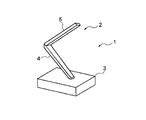
本実施形態のプローブカード1は、例えば図1に示すように、接続端子3aを有する配線板3およびプローブ2を備えている。
本実施形態のプローブ2は、複数のビーム部(例えば4、5など)で構成されたばね部を有する。このばね部においては、図1または図2に示すように、第1ビーム部4から第nビーム部(nは2以上の任意の整数である。)(部品番号は5、6、またはNである。)までの複数のビーム部が傾斜配置または水平配置されている。傾斜配置されたビーム部を例えば図1に示すように第2傾斜ビーム部5と称し、水平配置されたビーム部を例えば図3に示すように第2水平ビーム部6と称する。また、このばね部は、配線板3の接続端子3aに接続された第1ビーム部4から第nビーム部Nまでの各端部を一体形成された各々のヒンジ部H(図1参照)として複数のビーム部を順次連結させることにより、シングルアームパンタグラフ形状に形成されている。このばね部は、図3または図4に示すように、Z字形状に形成されていても良い。また、ばね部のシングルアームパンタグラフ形状またはZ字形状は、図1または図3に示すように単独であっても良いし、図2または図4に示すように連続しても良い。
ビーム部(例えば4)は、所定の幅を有する板形状にそれぞれ形成されている。このビーム部(例えば4)は、多角形板、円形板、楕円形板その他の一端または両端の幅が中間部の幅よりも狭い板状に形成されていることが好ましい。また、このビーム部(例えば4)は、ドーナツ形状に形成されていることがなお好ましい。
ビーム部の接触箇所(例えば5a、6a、Na)は、図1、図3または図4に示すように、プローブ2の接触部として接触対象となる電極パッド(図示せず)に接触する。このビーム部の接触箇所(例えば5a、6a、Na)は、電極パッドと平行に形成されていることが好ましい。
第1傾斜ビーム部4は、配線板3の接続端子3aに対して直接的に接続されていても良いし、間接的に接続されていても良い。例えば、プローブ2は、図2または図4に示すように、配線板3の接続端子3aと第1ビーム部4との間に、金属製の嵩上台8を有していても良い。この嵩上台8は、配線板3から第1ビーム部4を電極パッドの配設側(上方)に嵩上げするものであって、第1傾斜ビーム部4と配線板3の接続端子3aとを間接的に接続する。
また、プローブ2は、図3または図4に示すように、水平ビーム部9を有していても良い。この水平ビーム部9は、嵩上台8から水平方向に延在して形成されており、嵩上台8と第1ビーム部4の下端とを接続するものである。
さらに、プローブ2は、図5に示すように、垂直接続部25を有していても良い。垂直接続部25は、柱状に形成されており、上下方向に隣位する各ビーム部の各端部の間、例えば、第1傾斜ビーム部4の上端と第2ビーム部5(または6)の下端との間に介在している。
本実施形態のプローブカード1のプローブ2は種々の方法で形成することができる。例えば、本実施形態のプローブ2は、必須の工程として、図6Aに示すような穴10aの内部に第1傾斜ビーム部4がめっき形成される第1レジストめっき型の形成、図6Bに示すような第1傾斜ビーム部4のめっき形成、図6Cに示すような第1レジストめっき型の除去、図6Dに示すような上面が平らな第1レジスト埋込台座の形成、図6Eに示すような穴15aの内部に第2傾斜ビーム部5がめっき形成される第2レジストめっき型の形成、図6Fに示すような第2ビーム部5(または6)のめっき形成および図6Gに示すようなレジストの除去を経て、形成される。
また、本実施形態のプローブ2は、任意の追加工程として、図7に示すような第1レジストめっき型の形成前に嵩上台8用レジストめっき型20および嵩上台8のめっき形成、図8および図9に示すような第1レジストめっき型の形成前に水平ビーム部9用レジストめっき型21および水平ビーム部9めっきの形成ならびに図10に示すような垂直接続部25のめっき形成を経て、形成されていても良い。
次に、本実施形態のプローブカード1の作用を説明する。
本実施形態のプローブカード1において、プローブ2のばね部は、例えば図1に示すように、複数のビーム部4、5を上下に段組することにより、単独の(または図2のように連続した)シングルアームパンタグラフ形状(または図3または図4に示すZ字形状)に形成されている。そのため、狭小の有効スペースでプローブ2のストローク長さを長くすることができる。
前述の各ビーム部(例えば4、5)は、所定の幅を有する板形状にそれぞれ形成されている。そのため、図11または図12に示すような直線状またはC形状のビーム部(例えば4、5)を組み合わせてなるプローブ2とは異なり、プローブ2の収縮時にプローブ2が不必要に水平方向に動いてプローブの伸縮動作の挙動を乱してしまうことを防止することができる。
また、ビーム部は、図13に示すように、多角形板、円形板、楕円形板その他の一端または両端の幅が中間部の幅よりも狭い板状に形成されていることが好ましい。この場合、図11または図12に示すような幅の狭い線状またはC形状のビーム部(例えば4、5)を有するプローブ2よりもその弾性力を大きくすることができる。また、ビーム部の中間部の幅を上下両端の幅よりも大きくすることにより、プローブ2のばね部の収縮量に応じて弾性力を大きくさせるといったようなプローブ2の弾性力の制御を容易にすることができる。
特に、図1から図4に示すように、ビーム部がドーナツ形状に形成されていることがより好ましい。こうすれば、各ビーム部の内部に設けられた孔の大きさによってプローブ2に印加された低荷重により生じるプローブ2の弾性力を減少方向に調整することが容易になるので、プローブ2の全幅を大きくしてもプローブ2が生じる弾性力を小さくすることができる。これにより、プローブ2の全幅の拡大によるプローブ2の収縮方向への挙動安定性を向上させるとともに、プローブ2の弾性力の制御を容易にすることができる。
また、例えば、図1の第2ビーム部5(または6)の上端のように、ビーム部の接触箇所(例えば5a、6a、Na)は、電極パッドと平行に形成されていることが好ましい。これにより、電極パッドとの接触面積を大きくすることができる。
また、プローブ2は、図2または図4に示すように、嵩上台8を有していることが好ましい。嵩上台8を形成することにより、第1傾斜ビーム部4が配線板3に早期に底付きしてしまうことを抑制することができる。
嵩上台8を形成する場合、プローブ2には水平ビーム部9が形成されていることが好ましい。水平ビーム部9が変形してもビーム部の接触箇所(例えば5a、6a、Na)の位置が左右にずれることが少ないので、プローブ2の弾性力を水平ビーム部9の追加により制御しつつ、プローブ2の弾性変形の挙動制御を容易に行なうことができる。
さらに、このプローブ2には、図5に示すように、垂直接続部25が形成されていることが好ましい。各ビーム部(例えば4、5)の間に垂直接続部25が介在することによって各ビーム部(例えば4、5)の間から界面剥離することを防止することができる。
すなわち、本実施形態のプローブカード1によれば、プローブ2のばね部を構成するビーム部の形状、それらの段組形状などを上記の通りにしたので、プローブ2に加える荷重を低く維持したまま、狭小の有効スペースでプローブ2のストローク長さを長くし、かつ、プローブ2が安定して伸縮動作することができるという効果を奏する。
なお、本発明は、前述した実施形態などに限定されるものではなく、必要に応じて種々の変更が可能である。
1 プローブカード
2 プローブ
3 配線板
4 第1傾斜ビーム部
5 第2傾斜ビーム部
6 第2水平ビーム部
7 第3傾斜ビーム部
8 嵩上台
9 水平ビーム部
2 プローブ
3 配線板
4 第1傾斜ビーム部
5 第2傾斜ビーム部
6 第2水平ビーム部
7 第3傾斜ビーム部
8 嵩上台
9 水平ビーム部
Claims (7)
- 接続端子を有する配線板と、
所定の幅を有する板形状にそれぞれ形成された第1ビーム部から第nビーム部(nは2以上の任意の整数である。)までの複数のビーム部を傾斜配置または水平配置し、かつ、前記配線板の接続端子に直接的または間接的に接続された前記第1ビーム部から前記第nビーム部までの各端部を各々のヒンジ部として前記複数のビーム部を順次連結させることにより、単独のまたは連続したシングルアームパンタグラフ形状またはZ字形状に形成されているばね部を有するプローブと
を備えることを特徴とするプローブカード。 - 前記ビーム部は、多角形板、円形板、楕円形板その他の一端または両端の幅が中間部の幅よりも狭い板状に形成されている
ことを特徴とする請求項1に記載のプローブカード。 - 前記ビーム部は、ドーナツ形状に形成されている
ことを特徴とする請求項2に記載のプローブカード。 - 前記プローブの接触部として接触対象となる電極パッドに接触する前記ビーム部の接触箇所は、前記電極パッドと平行に形成されている
ことを特徴とする請求項1に記載のプローブカード。 - 前記プローブは、前記配線板の接続端子と前記第1ビーム部との間において前記配線板から前記第1ビーム部を前記電極パッドの配設側に嵩上げする嵩上台を有している
ことを特徴とする請求項1に記載のプローブカード。 - 前記プローブは、前記嵩上台から水平方向に延在して形成されており、前記嵩上台と前記第1ビーム部の下端とを接続する水平ビーム部を有している
ことを特徴とする請求項5に記載のプローブカード。 - 前記プローブは、上下方向に隣位する前記各ビーム部の各端部の間を接続しており、柱状に形成されている垂直接続部を有している
ことを特徴とする請求項1に記載のプローブカード。
Applications Claiming Priority (2)
| Application Number | Priority Date | Filing Date | Title |
|---|---|---|---|
| JP2009-094148 | 2009-04-08 | ||
| JP2009094148A JP2012137292A (ja) | 2009-04-08 | 2009-04-08 | プローブカード |
Publications (1)
| Publication Number | Publication Date |
|---|---|
| WO2010117034A1 true WO2010117034A1 (ja) | 2010-10-14 |
Family
ID=42936315
Family Applications (1)
| Application Number | Title | Priority Date | Filing Date |
|---|---|---|---|
| PCT/JP2010/056361 Ceased WO2010117034A1 (ja) | 2009-04-08 | 2010-04-08 | プローブカード |
Country Status (2)
| Country | Link |
|---|---|
| JP (1) | JP2012137292A (ja) |
| WO (1) | WO2010117034A1 (ja) |
Citations (4)
| Publication number | Priority date | Publication date | Assignee | Title |
|---|---|---|---|---|
| JPH1019071A (ja) * | 1996-07-01 | 1998-01-20 | Yoshino Kogyosho Co Ltd | 合成樹脂製圧縮スプリング |
| JPH1047400A (ja) * | 1996-05-29 | 1998-02-17 | Yoshino Kogyosho Co Ltd | 合成樹脂製スプリング |
| JP2003294787A (ja) * | 2002-04-01 | 2003-10-15 | Fujitsu Ltd | コンタクタ、その製造方法及びコンタクタを用いた試験方法 |
| JP2008281519A (ja) * | 2007-05-14 | 2008-11-20 | Alps Electric Co Ltd | プローブカードおよびその製造方法 |
-
2009
- 2009-04-08 JP JP2009094148A patent/JP2012137292A/ja not_active Withdrawn
-
2010
- 2010-04-08 WO PCT/JP2010/056361 patent/WO2010117034A1/ja not_active Ceased
Patent Citations (4)
| Publication number | Priority date | Publication date | Assignee | Title |
|---|---|---|---|---|
| JPH1047400A (ja) * | 1996-05-29 | 1998-02-17 | Yoshino Kogyosho Co Ltd | 合成樹脂製スプリング |
| JPH1019071A (ja) * | 1996-07-01 | 1998-01-20 | Yoshino Kogyosho Co Ltd | 合成樹脂製圧縮スプリング |
| JP2003294787A (ja) * | 2002-04-01 | 2003-10-15 | Fujitsu Ltd | コンタクタ、その製造方法及びコンタクタを用いた試験方法 |
| JP2008281519A (ja) * | 2007-05-14 | 2008-11-20 | Alps Electric Co Ltd | プローブカードおよびその製造方法 |
Also Published As
| Publication number | Publication date |
|---|---|
| JP2012137292A (ja) | 2012-07-19 |
Similar Documents
| Publication | Publication Date | Title |
|---|---|---|
| EP3740765B1 (en) | Cantilever contact probe and corresponding probe head | |
| KR102232789B1 (ko) | 멀티-레이어 mems 스프링 핀 | |
| US7619497B2 (en) | Electrostatic relay | |
| JP6084974B2 (ja) | Memsデバイス用の結合脚及びセミフレキシブルなアンカリング | |
| JP4580745B2 (ja) | 圧電駆動型mems装置 | |
| US11442080B2 (en) | Contact probe and relative probe head of an apparatus for testing electronic devices | |
| JP2009036744A (ja) | 複数梁合成型接触子 | |
| EP3528272B1 (en) | Micro-electro-mechanical switch beam construction with minimized beam distortion and method for constructing | |
| JP2012242178A (ja) | バーチカルプローブおよびそれを用いたプローブヘッド | |
| JP2016053529A (ja) | 板状体の支持構造 | |
| JP2023091519A5 (ja) | ||
| EP2556014B1 (en) | Micro-electro-mechanical switch beam construction with minimized beam distortion and method for constructing | |
| KR101865756B1 (ko) | 짧은 스크럽마크를 위한 프로브 카드의 다중 캔틸레버 빔 구조체 및 그 제조방법 | |
| WO2010117034A1 (ja) | プローブカード | |
| JP5886694B2 (ja) | カンチレバー型プローブとそれを備えるプローブカード又はプローブユニット | |
| JP6854245B2 (ja) | 基板移載用ハンド | |
| JP4884475B2 (ja) | 電気的接続体 | |
| JP2009300190A (ja) | プローブ | |
| JP5462732B2 (ja) | シート状コネクタ、及びその製造方法 | |
| WO2020026489A1 (ja) | 圧接コンタクト | |
| JP2010261777A (ja) | プローブカードおよびその製造方法 | |
| KR101790931B1 (ko) | 처짐 방지를 위한 보강형 프로브 카드의 다중 캔틸레버 빔 구조체 및 그 제조방법 | |
| JP5798094B2 (ja) | アクチュエータ | |
| JP5808147B2 (ja) | 部品実装方法および基板 | |
| JP2006030585A (ja) | 薄膜部材、マイクロアクチュエータ、光学装置及び光スイッチ |
Legal Events
| Date | Code | Title | Description |
|---|---|---|---|
| 121 | Ep: the epo has been informed by wipo that ep was designated in this application |
Ref document number: 10761733 Country of ref document: EP Kind code of ref document: A1 |
|
| NENP | Non-entry into the national phase |
Ref country code: DE |
|
| 122 | Ep: pct application non-entry in european phase |
Ref document number: 10761733 Country of ref document: EP Kind code of ref document: A1 |
|
| NENP | Non-entry into the national phase |
Ref country code: JP |