WO2010110398A1 - 光再構成型ゲートアレイの再構成制御装置及びホログラムメモリの情報読出装置 - Google Patents
光再構成型ゲートアレイの再構成制御装置及びホログラムメモリの情報読出装置 Download PDFInfo
- Publication number
- WO2010110398A1 WO2010110398A1 PCT/JP2010/055292 JP2010055292W WO2010110398A1 WO 2010110398 A1 WO2010110398 A1 WO 2010110398A1 JP 2010055292 W JP2010055292 W JP 2010055292W WO 2010110398 A1 WO2010110398 A1 WO 2010110398A1
- Authority
- WO
- WIPO (PCT)
- Prior art keywords
- laser
- light
- micromirror
- angle
- unit
- Prior art date
- Legal status (The legal status is an assumption and is not a legal conclusion. Google has not performed a legal analysis and makes no representation as to the accuracy of the status listed.)
- Ceased
Links
Images




Classifications
-
- G—PHYSICS
- G03—PHOTOGRAPHY; CINEMATOGRAPHY; ANALOGOUS TECHNIQUES USING WAVES OTHER THAN OPTICAL WAVES; ELECTROGRAPHY; HOLOGRAPHY
- G03H—HOLOGRAPHIC PROCESSES OR APPARATUS
- G03H1/00—Holographic processes or apparatus using light, infrared or ultraviolet waves for obtaining holograms or for obtaining an image from them; Details peculiar thereto
- G03H1/26—Processes or apparatus specially adapted to produce multiple sub- holograms or to obtain images from them, e.g. multicolour technique
- G03H1/30—Processes or apparatus specially adapted to produce multiple sub- holograms or to obtain images from them, e.g. multicolour technique discrete holograms only
-
- G—PHYSICS
- G03—PHOTOGRAPHY; CINEMATOGRAPHY; ANALOGOUS TECHNIQUES USING WAVES OTHER THAN OPTICAL WAVES; ELECTROGRAPHY; HOLOGRAPHY
- G03H—HOLOGRAPHIC PROCESSES OR APPARATUS
- G03H1/00—Holographic processes or apparatus using light, infrared or ultraviolet waves for obtaining holograms or for obtaining an image from them; Details peculiar thereto
- G03H1/0005—Adaptation of holography to specific applications
-
- H—ELECTRICITY
- H04—ELECTRIC COMMUNICATION TECHNIQUE
- H04Q—SELECTING
- H04Q2213/00—Indexing scheme relating to selecting arrangements in general and for multiplex systems
- H04Q2213/1301—Optical transmission, optical switches
Definitions
- the present invention relates to a reconstruction control device for an optically reconfigurable gate array and an information reading device for a hologram memory.
- an optically reconfigurable gate array (ORGA) has been proposed as a device for reconfiguring a logic operation cell into various logic circuits when irradiated with light.
- ORGA optically reconfigurable gate array
- a large amount of circuit information is required. Therefore, the 32nd paragraph of Japanese Patent No. 4033818 (JP4033818B2) and the 69th paragraph of Japanese Patent No. 411138 (JP412138B2) disclose the use of, for example, a hologram memory as an optical memory for storing this circuit information. Yes.
- the hologram memory has a very large capacity and can store extremely huge circuit information reaching 3 Tbits (terabit).
- 1 Tbit is 10 12 bits, and 3 Tbit corresponds to a circuit scale of 1 trillion gates.
- the storage capacity is large, there is a problem that if it takes time to transfer circuit information, it takes time to reconfigure the logic operation cells.
- An information reading device for a hologram memory that reads out circuit information from the hologram memory at high speed
- an optical reconfiguration type that reads out circuit information from the hologram memory at high speed.
- An object of the present invention is to provide an optical reconstruction control device for an optically reconfigurable gate array capable of optically reconfiguring a gate array.
- a laser irradiation unit having a plurality of laser emission units arranged in a straight line, and each of the laser emission units corresponds to each row of a matrix.
- the hologram memory is configured as a hologram memory that is irradiated with laser light from a scanning unit and reads an optical pattern based on pre-recorded circuit information, and a single light receiving unit in which a plurality of light receiving elements are arranged in an array.
- a plurality of logic operation cells arranged in an array are reconfigured into various logic operation circuits based on the light pattern read out from the light and received by the light receiving unit.
- a plurality of optically reconfigurable gate arrays and a plurality of laser arrays that are arranged in rows corresponding to the laser emitting units from which the laser beams are emitted from any one or a plurality of laser emitting units of the laser emitting units.
- a control unit that adjusts an angle of any one of the micromirrors and controls the micromirrors to reflect the laser light.
- the hologram memory information reading device includes a laser irradiation unit having a plurality of laser emission units arranged linearly, and the laser emission unit corresponding to each row of the matrix.
- a laser beam scanning unit that has a plurality of micromirrors arranged in a matrix and scans the laser beam emitted from the laser emission unit by adjusting the angle of each micromirror, and the laser beam scanning unit
- a hologram memory from which a light pattern based on pre-recorded information is read out, and laser light is emitted from one or a plurality of laser emitting units of the laser irradiating unit, By adjusting the angle of any one of the plurality of micromirrors arranged in a row corresponding to the emitted laser emitting portion, Control to reflect the laser beam to the micromirror and adjust the angle of the micromirror in a row corresponding to the laser emitting unit from which the laser beam is not emitted within a period in which no laser is emitted from the laser
- the laser beam is emitted from any one or a plurality of laser emission units of the laser irradiation unit, and among the plurality of micromirrors arranged in a row corresponding to the laser emission unit from which the laser beam was emitted, Control is performed to reflect the laser beam by adjusting the angle of any one of the micromirrors, and information is read from the hologram memory at high speed.
- the optical reconstruction gate array reconstruction control device of the present invention can read out circuit information from the hologram memory at high speed and perform optical reconstruction.
- the hologram memory information reading device of the present invention can read circuit information from the hologram memory at high speed.
- FIG. 1 is a diagram showing a configuration of a reconstruction control device for an optical reconstruction gate array according to an embodiment of the present invention.
- An optical reconstruction gate array reconstruction control device includes a laser array 1 having a plurality of laser emission units, a micromirror array device 3 having micromirrors that can be controlled independently, and circuit information stored as a hologram. And a hologram memory 4 from which an optical pattern indicating circuit information is read out when irradiated with laser light.
- a volume hologram memory may be used as the hologram memory 4.
- the volume hologram memory can record T-bit order information by multiplex recording a plurality of holograms.
- angle multiplexing is used as the multiplex recording method, it is possible to individually read out the multiplex recorded holograms by changing the angle of the readout light in accordance with the angle of the reference light.
- the reconstruction controller for the optical reconstruction gate array includes an optical reconstruction gate array 9 that performs optical reconstruction when the light pattern from the hologram memory 4 is irradiated, a laser beam emission timing of the laser array 1, and a micromirror. And a control device 10 for controlling the angle.
- the laser array 1 has a plurality of laser emitting portions arranged in a straight line. The laser emission timing and the emission period from each laser emission unit are controlled by the control device 10.
- the laser array 1 is connected to the control device 10 via a laser driver (not shown), and the laser driver drives each laser of the laser array 1 to light independently according to a control signal from the control device 10. .
- the micromirror array device 3 is a so-called MEMS (Micro-Electro-Mechanical System).
- the micromirror array device 3 has a plurality of micromirrors arranged in a matrix. Note that the angle of each micromirror (the angle in the normal direction with reference to the case of zero displacement) and the angular displacement speed are controlled by the control device 10. Also, power is supplied from a power source (not shown) to each of the electrically driven parts such as the laser array 1 and the micromirror array device 3.
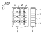
- FIG. 2 is a plan view of the laser array 1 and the micromirror array device 3. As shown in the figure, each row of micromirrors arranged in a matrix corresponds to each of the laser emission portions 1A, 1B, 1C, 1D,.
- the laser array 1 has 100 laser emission units
- the micromirror array device 3 has a plurality of micromirrors configured in a matrix of 100 rows.
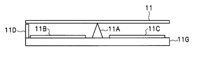
- FIG. 3A is a cross-sectional view showing a state in which the micromirror 11 is not displaced
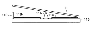
- FIG. 3B is a cross-sectional view showing a state in which the micromirror 11 is displaced.
- the other micromirrors are configured in the same manner as in FIGS. 3A and 3B, the micromirror 11 will be described as an example here.
- the micromirror array device 3 is provided symmetrically with respect to the micromirror 11, the support portion 11A that supports the center portion of the micromirror 11, and the support portion 11A, and is separated from the micromirror 11 by a predetermined distance. Electrodes 11B and 11C, a stopper 11D provided on the electrode 11B side, and a support 11A, electrodes 11B and 11C, and a substrate 11G that holds the stopper 11D are provided. When the mirror angle of the micro mirror 11 is zero, one end side (the electrode 11B side) of the micro mirror 11 is in contact with the stopper 11D.
- the angular displacement time varies depending on the product, but is, for example, 1 ⁇ s (microseconds) or less for ⁇ 10 degrees and 30 ⁇ s or less for ⁇ 45 degrees.
- the micromirror array device 3 having 2 million pixels and responding in 200 ⁇ s has already been commercialized.
- emission timing of the laser beam from the laser array 1 and the angle of the micromirror of the micromirror array device 3 have the following relationship.
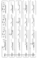
- FIG. 4 is a diagram showing the relationship between the laser beam emission timing and the micromirror angle.
- each micromirror is continuously adjusted to an arbitrary angle as follows.
- the mirror angles of the second micromirrors 12, 22, 32, and 42 are set to arbitrary angles with the position farthest from the laser array 1 as a reference. Then, only the laser beam emitting portion 1A is turned on (lighted state) and emits the laser beam. Thereby, the laser beam emitted from the laser beam emitting unit 1A is reflected by the micromirror 12.
- the laser beam emitting unit 1A is turned off (lights off), and only the laser beam emitting unit 1B is turned on. Then, while the laser beam emitting portion 1A is not lighting the laser beam, the angle of the micromirror 12 is adjusted and the mirror beam moves toward a position where the mirror angle becomes zero.
- the angle of the micromirror 12 is adjusted and the mirror angle moves toward a position where the mirror angle becomes zero. As described above, the angle of the micromirror is adjusted during a period in which the laser beam is not emitted from the laser beam emitting unit corresponding to the row of the micromirror.
- circuit information for reconfiguring the logical operation cells of the optical reconfigurable gate array 9 is recorded. Then, when the hologram memory 4 is irradiated with laser light from the micromirror array device 3, an optical pattern is read from the hologram memory 4 and irradiated to the light reconstruction gate array 9.
- the optical reconstruction gate array 9 includes a single light receiving unit including a plurality of photodiodes, and receives a light pattern from the hologram memory 4 by the light receiving unit, so that a plurality of logical operation cells arranged in an array are variously used.
- the logic operation circuit is reconfigured.
- the optical reconstruction gate array 9 is an LSI unit that mounts a circuit by optical reconstruction.
- the LSI unit includes a logic block structure, a switch matrix structure, and a plurality of photodiodes.
- a plurality of photodiodes arranged in the LSI unit receive circuit information in parallel by irradiating the light pattern, whereby optical reconstruction is performed in the LSI unit.
- the light receiving unit may be a photodiode array as described above or an image sensor as long as it can receive a light pattern. That is, it may be composed of a light receiving element other than a photodiode.
- the emission timing of the laser light is controlled as follows.
- FIG. 5 is a timing chart showing the laser beam emission timing and the micromirror angle adjustment timing.
- the laser emitting portions 1A, 1B, and 1C of the laser array 1 will be described as examples.
- Each micromirror is continuously adjusted to an arbitrary angle of 0 to 30 degrees.
- the laser beam from the laser beam emitting unit 1A is turned on.
- the angle of the micromirror 11 is 20 degrees, and the angles of the micromirrors 12 and 13 are zero degrees.
- the area A1 of the hologram memory 4 is irradiated with laser light at an angle of 20 degrees, and the light pattern is read out.
- the angle of the micromirror 11 is changed from 20 degrees to 10 degrees by the end of the period T3.
- the laser beam from the laser beam emitting unit 1B is turned on.
- the angle of the micromirror 21 is 20 degrees, and the angles of the micromirrors 22 and 23 are zero degrees.
- the region B1 of the hologram memory 4 is irradiated with laser light at an angle of 20 degrees, and the light pattern is read out.
- the angle of the micromirror 21 is changed from 20 degrees to zero degrees and the angle of the micromirror 23 is changed from zero degrees to 10 degrees by the end of the period T4.
- the laser beam from the laser beam emitting unit 1C is turned on.
- the angle of the micromirror 31 is 20 degrees, and the angles of the micromirrors 32 and 33 are zero degrees.
- the region C1 of the hologram memory 4 is irradiated with laser light at an angle of 20 degrees, and the light pattern is read out. Note that the angles of the micromirrors 31, 32, and 33 do not change in any period.
- the laser beam from the laser beam emitting unit 1A is turned on again.
- the angle of the micromirror 11 is 10 degrees, and the angles of the micromirrors 12 and 13 are zero degrees.
- the region A1 of the hologram memory 4 is irradiated with laser light at an angle of 10 degrees, and the light pattern is read out.
- the angle of the micromirror 11 is changed from 10 degrees to zero degrees and the angle of the micromirror 12 is changed from zero degrees to 30 degrees by the end of the period T6.
- the laser beam from the laser beam emitting unit 1B is turned on again.
- the angle of the micromirror 23 is 10 degrees, and the angles of the micromirrors 21 and 22 are zero degrees.
- the region B3 of the hologram memory 4 is irradiated with laser light at an angle of 10 degrees, and the light pattern is read out.
- the laser beam from the laser beam emitting unit 1C is turned on again.
- the region C1 of the hologram memory 4 is irradiated with laser light at an angle of 20 degrees, and the light pattern is read out.
- the laser beam from the laser beam emitting unit 1A is turned on again.
- the region A2 of the hologram memory 4 is irradiated with laser light at an angle of 30 degrees, and the light pattern is read out.
- the laser beam emitting section from which the laser beam is emitted from the laser array 1 is sequentially switched.
- the angle of the micromirror is adjusted while the laser beam is emitted from the laser beam emitting unit corresponding to another row.
- different regions of the hologram memory 4 are irradiated with laser light, or the same region of the hologram memory 4 is irradiated with different angles, and an optical pattern indicating circuit information is read out.
- the optical reconfiguration gate array 9 receives the optical pattern read from the hologram memory 4 in this way, and reconfigures a plurality of logical operation cells arranged in an array into various logical operation circuits.
- the optically reconfigurable gate array reconfiguration controller is good at switching laser light by the laser array 1 that is good at high-speed switching and low-speed switching but is good at large-capacity addressing.
- the circuit information is read out from the hologram memory 4 at high speed and continuously, and the optical reconstruction gate array 9 is moved at high speed based on this circuit information. Can be reconfigured.
- FIG. 6 is a diagram showing a configuration of a circuit information recording device of an optically reconfigurable gate array when circuit information is recorded in the hologram memory 4.
- a spatial light modulator 19 is provided in place of the optically reconfigurable gate array 9 at the position of the optically reconfigurable gate array 9 shown in FIG.
- An image pattern is formed on the spatial light modulator 19 based on circuit information.
- a half mirror 2 that separates laser light from the laser array 1 into transmitted light (light for reference light) and reflected light (light for signal light), and a half mirror 2
- the mirror 5 and the mirror 6 that reflect the light reflected from the mirror 6 in a predetermined direction, and the lens 7 and the lens 8 that expand the beam diameter of the laser light from the mirror 6 are provided.
- the half mirror 2 transmits a part of the laser light emitted from the laser array 1 and reflects the remaining laser light. Then, the laser light transmitted through the half mirror 2 is irradiated to the micromirror array device 3 as reference light. Further, the laser light reflected by the half mirror 2 is applied to the mirror 5 as light for signal light. The reference light is reflected by the micromirror array device 3 and then irradiated to the hologram memory 4.
- the signal light is reflected by the mirror 5, then the beam diameter is enlarged by the lenses 7 and 8 via the mirror 6, and then irradiated to the spatial light modulator 19.
- the signal light is modulated by the spatial light modulator 19 according to the image pattern, and signal light on which circuit information is superimposed is generated.
- the signal light on which the circuit information is superimposed is irradiated onto the hologram memory 4.
- the signal light and the reference light cause optical interference in the recording layer of the hologram memory 4, and the image pattern formed by the spatial light modulator 19 is recorded as interference fringes (ie, holograms).
- circuit information of the optical reconstruction gate array 9 is recorded in the hologram memory 4.
- FIG. 7A is a diagram showing the response characteristics of the micromirror
- FIG. 7B is a diagram showing the response characteristics of the micromirror and the lighting timing of the laser light pulse.
- the micromirror having the configuration shown in FIG. 2 changes its angle according to a predetermined response curve after voltage application to the electrodes. Therefore, the control device 10 shown in FIG.
- the laser beam controls the micromirror array device 3 so that a voltage is applied to the electrodes at a predetermined timing, and the laser beam is irradiated so that a laser beam is irradiated after a certain period of time.
- the array 1 is controlled.
- the laser beam can be irradiated in an analog manner at an arbitrary angle, and information on the hologram memory corresponding to the angle can be read out.
- the angle of the micromirror is ⁇ 40 degrees when the laser beam is irradiated at time t1, and becomes +10 degrees when the laser beam is irradiated at time t2.
- the pulse width can be controlled even if it is 1 ns or less, for example, when considering a micromirror that responds in 1 ⁇ s, the switching angle resolution becomes 1000 or more.
- FIG. 8 is a timing chart showing the potential of the electrode 11B, the potential of the electrode 11C, the mirror angle, and the timing of laser emission. As shown in the figure, analog modulation can be realized if a predetermined voltage is applied to the electrodes and laser light is emitted in consideration of transient response.
- FIG. 9A is a diagram showing a method of reading information by always turning on the laser
- FIG. 9B is a diagram showing a method of reading information by turning on the laser pulse.
- the curves shown in FIGS. 9A and 9B represent the response characteristics of the micromirror, as in FIGS. 7A and 7B.
- the laser array 1 is continuously lit or pulsed by the control device 10 of FIG.
- a part of the information of the photosensor of the optical reconstruction gate array 9 (or image sensor) is used for reading the identifier, and information corresponding to the identifier is read based on the information of the identifier.
- the laser irradiation angle is continuously changed, the timing at which the laser irradiation angle coincides with the angle at which the information in the hologram memory can be read is detected from the identifier information, and the information is read out at that timing, thereby The hologram memory information at different angles can be read out.
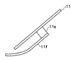
- FIG. 10A is a diagram showing a state of a piezo element type micromirror array device at rest
- FIG. 10B is a diagram showing a state at the time of angle adjustment.
- the micromirror array device 3 includes a micromirror 11, a support portion 11e that supports the micromirror 11, and a piezo element 11f having the support portion 11e fixed to the tip portion. .
- the piezo element 11f is bent and the angle of the micromirror 11 is changed.
- the angle of the micromirror of the micromirror array device 3 can be adjusted in an analog manner, for example, from about 0 to 7 degrees, and the response speed is, for example, 1 degree / ⁇ s.
- FIG. 11 is a diagram showing the response of the photodiodes of the optical reconstruction gate array 9. If the contrast value (difference between high level and low level) of each bit of the context identification information (circuit information identification information) is a certain level or more, the control device 10 shown in FIG. 1 determines that the irradiation angle is correct, It is possible to identify which context (circuit information) is read from this information. Further, even when the angular response of the micromirror array device 3 cannot be sensed, the context is accurately read out. For example, when the irradiation angle of the laser beam to the hologram memory 4 is correct, as shown in FIG. 11, the information “1” is settled at a high level, and the information “0” is settled at a low level. FIG. 11 shows a high level state. Thus, if the irradiation angle matches the correct angle, the contrast value becomes a predetermined value or more, and if the irradiation angle does not match the correct angle, the contrast value becomes an intermediate value.
- the angle of the micromirror can be inferred from the applied voltage because it is voltage dependent in the case of the piezo type, and can be inferred by measuring the time because it is time dependent in the case of the binary type. However, it may not be uniquely determined due to the influence of temperature, voltage fluctuation, deterioration, or the like, in which case the blind detection method is effective.
- a countermeasure when “always lighting failure” occurs in a part of the laser array will be described.
- the reconstruction controller for the optical reconstruction gate array shown in FIG. 1 a part (laser) of the laser array 1 having a plurality of laser emitting portions fails in the always-on mode due to problems such as transistor thermal melting. In such a case, it becomes difficult to read out another hologram due to the laser beam emitted from the failed laser emission unit.
- the plurality of laser emitting portions of the laser array 1 are divided into a plurality of groups in advance and are configured to be driven by a common power source for each group. If detected, the laser array 1 may be controlled so that all of the plurality of laser emitting units belonging to the same set as the failed laser emitting unit are turned on (lighted state).
- the plurality of laser emitting units belonging to the set significantly reduce the irradiation energy (laser power) of the emitted laser light?
- the drive current becomes lower than the threshold current of the laser, the light is turned off. Thereby, it is possible to read out another hologram by the laser light emitted from the laser emitting units belonging to another group.
- the always-on failure can be detected by, for example, “error detection” when the light pattern is received by the light receiving unit of the optical reconstruction gate array 9 by adding an error detection code to the circuit information. “Error detection” is executed by the control device 10 based on information acquired from the light receiving unit of the optical reconstruction gate array 9.
- the same circuit information is read by irradiating the laser beam from the laser emitting unit belonging to another set. It is preferable to give redundancy to the circuit information stored in the hologram memory 4 so that it can be output.
- the laser array 1 is used as means for irradiating laser light, but the present invention is not limited to this.
- a rotating polygon mirror (polygon mirror) scans laser light emitted from a single laser at an equal angle, and an f ⁇ lens scans the laser beam scanned at an equal angle on the reflection surface of the micromirror array device 3. You may scan at a constant speed.
- the laser array 1 emits a plurality of laser beams at the same time, and the micromirror array device 3 transmits the plurality of laser beams from the laser array 1 in predetermined directions, respectively. It may be reflected.
Landscapes
- Physics & Mathematics (AREA)
- General Physics & Mathematics (AREA)
- Holo Graphy (AREA)
- Optical Head (AREA)
- Optical Recording Or Reproduction (AREA)
Abstract
光再構成型ゲートアレイの再構成制御装置は、レーザアレイ(1)と、マトリクス状に配列された複数のマイクロミラーを有するマイクロミラー・アレイ・デバイス(3)と、マイクロミラー・アレイ・デバイス(3)のレーザ光が照射され、予め記録された回路情報に基づく光パターンが出力されるホログラムメモリ(4)と、ホログラムメモリ(4)からの光パターンに基づいて、アレイ状に配列された複数の論理演算セルを各種の論理演算回路に再構成する光再構成型ゲートアレイ(9)と、レーザアレイ(1)のいずれか1つもしくは複数のレーザ出射部からレーザ光を出射させ、レーザ光が出射されたレーザ出射部に対応する行に配列された複数のマイクロミラーのうち、何れか1つのマイクロミラーの角度を調整して、当該マイクロミラーにレーザ光を反射させる制御を行う制御装置(10)と、を備えている。
Description
本発明は、光再構成型ゲートアレイの再構成制御装置及びホログラムメモリの情報読出装置に関する。
従来、光が照射されると論理演算セルを各種の論理回路に再構成するデバイスとして光再構成型ゲートアレイ(ORGA:Optically Reconfigurable Gate Array)が提案されている。光再構成型ゲートアレイが再構成を行うためには大容量の回路情報が必要である。そこで、特許第4033818号公報(JP4033818B2)の第32段落や、特許第4121138号公報(JP4121138B2)の第69段落には、この回路情報を記憶する光メモリとして、例えばホログラムメモリを用いることが開示されている。
ホログラムメモリは、非常に大容量であり、3Tbit(テラビット)に達する超巨大な回路情報を記憶することが可能である。1Tbitは1012ビットであり、3Tbitは1兆ゲートの回路規模に相当する。しかし、記憶容量が大きくても、回路情報の転送に時間を要すれば、論理演算セルの再構成に時間がかかってしまうという問題がある。
ここで、転送速度が1Gbps(ギガビット/秒)に達する次世代のホログラムメモリを用いたとしても、1Tビットのデータの読み出しに2時間以上もかかってしまい、ホログラムメモリから大容量の回路情報を読み出すのは実用的ではない。
本発明は、上述した課題を解決するために提案されたものであり、ホログラムメモリから高速に回路情報を読み出すホログラムメモリの情報読出装置と、ホログラムメモリから高速に回路情報を読み出して光再構成型ゲートアレイの光再構成を行うことができる光再構成型ゲートアレイの光再構成制御装置と、を提供することを目的とする。
本発明に係る光再構成ゲートアレイの再構成制御装置は、直線状に配列された複数のレーザ出射部を有するレーザ照射部と、前記レーザ出射部の各々がマトリクスの各々の行に対応するように前記マトリクス状に配列された複数のマイクロミラーを有し、各々のマイクロミラーの角度を調整することで、前記レーザ出射部から出射されたレーザ光を走査するレーザ光走査部と、前記レーザ光走査部からのレーザ光が照射され、予め記録された回路情報に基づく光パターンが読み出されるホログラムメモリと、複数の受光素子がアレイ状に配列された単一の受光部として構成され、前記ホログラムメモリから読み出され前記受光部で受光された光パターンに基づいて、アレイ状に配列された複数の論理演算セルを各種の論理演算回路に再構成する光再構成型ゲートアレイと、前記レーザ照射部のいずれか1つもしくは複数のレーザ出射部からレーザ光を出射させ、前記レーザ光が出射されたレーザ出射部に対応する行に配列された複数のマイクロミラーのうち、何れか1つのマイクロミラーの角度を調整して、当該マイクロミラーに前記レーザ光を反射させる制御を行う制御部と、を備えている。
また、本発明に係るホログラムメモリの情報読出装置は、直線状に配列された複数のレーザ出射部を有するレーザ照射部と、前記レーザ出射部の各々がマトリクスの各々の行に対応するように前記マトリクス状に配列された複数のマイクロミラーを有し、各々のマイクロミラーの角度を調整することで、前記レーザ出射部から出射されたレーザ光を走査するレーザ光走査部と、前記レーザ光走査部からのレーザ光が照射され、予め記録された情報に基づく光パターンが読み出されるホログラムメモリと、前記レーザ照射部のいずれか1つもしくは複数のレーザ出射部からレーザ光を出射させ、前記レーザ光が出射されたレーザ出射部に対応する行に配列された複数のマイクロミラーのうち、何れか1つのマイクロミラーの角度を調整して、当該マイクロミラーに前記レーザ光を反射させ、レーザ光が出射されていないレーザ出射部に対応する行のマイクロミラーの角度を、前記レーザ出射部からレーザが出射されていない期間内に調整する制御を行う制御部と、複数の受光素子がアレイ状に配列され、前記ホログラムメモリから読み出された光パターンを受光する単一の受光部と、を備えている。
上記発明においては、レーザ照射部のいずれか1つもしくは複数のレーザ出射部からレーザ光を出射させ、レーザ光が出射されたレーザ出射部に対応する行に配列された複数のマイクロミラーのうち、何れか1つのマイクロミラーの角度を調整して、前記レーザ光を反射させる制御が行われて、ホログラムメモリから高速に情報が読み出される。
本発明の光再構成ゲートアレイの再構成制御装置は、ホログラムメモリから高速に回路情報を読み出して光再構成を行うことができる。また、本発明のホログラムメモリの情報読出装置は、ホログラムメモリから高速に回路情報を読み出すことができる。
以下、本発明の好ましい実施の形態について図面を参照しながら詳細に説明する。
[第1の実施形態]
図1は、本発明の実施の形態に係る光再構成ゲートアレイの再構成制御装置の構成を示す図である。
図1は、本発明の実施の形態に係る光再構成ゲートアレイの再構成制御装置の構成を示す図である。
光再構成ゲートアレイの再構成制御装置は、複数のレーザ出射部を有するレーザアレイ1と、各々独立に制御可能なマイクロミラーを有するマイクロミラー・アレイ・デバイス3と、回路情報がホログラムとして記憶され、レーザ光が照射されると回路情報を示す光パターンが読み出されるホログラムメモリ4と、を備えている。例えば、体積型ホログラムメモリを、ホログラムメモリ4として用いてもよい。体積型ホログラムメモリは、複数のホログラムを多重記録することで、Tビットオーダの情報を記録することが可能である。また、多重記録方法として「角度多重」を用いた場合には、参照光の角度に応じて読出し光の角度を変えて、多重記録されたホログラムを個別に読み出すことができる。
また、光再構成ゲートアレイの再構成制御装置は、ホログラムメモリ4からの光パターンが照射されると光再構成を行う光再構成ゲートアレイ9と、レーザアレイ1のレーザ光出射タイミング及びマイクロミラーの角度を制御する制御装置10と、を備えている。
レーザアレイ1は、直線状に配列された複数のレーザ出射部を有している。各レーザ出射部からのレーザ出射タイミング及び出射期間は、制御装置10により制御されている。なお、レーザアレイ1は、図示しないレーザドライバを介して制御装置10に接続されており、レーザドライバは制御装置10からの制御信号に応じてレーザアレイ1の各レーザを独立に点灯駆動している。
マイクロミラー・アレイ・デバイス3は、いわゆるMEMS(Micro-Electro-Mechanical Systems)である。マイクロミラー・アレイ・デバイス3は、マトリクス状に配列された複数のマイクロミラーを有している。なお、各マイクロミラーの角度(変位ゼロの場合を基準にした法線方向の角度)及び角度の変位速度は、制御装置10により制御されている。また、レーザアレイ1、マイクロミラー・アレイ・デバイス3等、電気的に駆動される各部には、図示しない電源から電力が供給されている。
図2は、レーザアレイ1とマイクロミラー・アレイ・デバイス3の平面図である。同図に示すように、マトリクス状に配列されたマイクロミラーの行の各々は、レーザアレイ1のレーザ出射部の各々1A、1B、1C、1D・・・に対応している。
例えば、1つのレーザ出射部1Aと1行分の複数のマイクロミラー11、12、13、14・・・とが1セットとなっており、全部で例えば100セットが実装されている。このため、本実施形態では、レーザアレイ1は100個のレーザ出射部を有し、マイクロミラー・アレイ・デバイス3は100行のマトリクス状に構成された複数のマイクロミラーを有している。
図3Aはマイクロミラー11が変位していない状態を示す断面図であり、図3Bはマイクロミラー11が変位した状態を示す断面図である。なお、他のマイクロミラーも図3A及び図3Bと同様に構成されているが、ここではマイクロミラー11を例に挙げて説明する。
マイクロミラー・アレイ・デバイス3は、マイクロミラー11と、マイクロミラー11の中心部を支持する支持部11Aと、支持部11Aに対して左右対称に設けられ、マイクロミラー11から所定距離だけ隔てられた電極11B、11Cと、電極11Bの側に設けられたストッパ-11Dと、支持部11A、電極11B、11C、ストッパ11Dを保持する基板11Gと、を備えている。マイクロミラー11のミラー角度がゼロの場合、マイクロミラー11の一端側(電極11Bの側)は、ストッパ11Dに接している。
そして、電極11B、11Cにそれぞれ所定の電圧が印加されると、マイクロミラー11と電極11B、11Cの電位差による静電力により、マイクロミラー11はストッパ11Dから離れて、マイクロミラー11の角度が調整される。なお、角度の変位時間は、製品によって異なるが、例えば±10度であれば1μs(マイクロ秒)以下、±45度であれば30μs以下である。
ここで、200万画素を有し、200μsで応答するマイクロミラー・アレイ・デバイス3が既に商品化されている。また、後述するが、各マイクロミラーの角度は角度制御をすることにより100個程度の角度分解能を持たせることができるため、各マイクロミラーは100個程度のアドレッシングに活用可能である。よって、1つのマイクロミラー・アレイ・デバイス3で操作できる実際のアドレス数は約2億(=100×200万画素)になる。これは、25Tビットのアクセス量に相当する。
一方、マイクロミラーのスイッチングは機械的に行われるため、スイッチングに200μs程度を要してしまうが、この点については、レーザアレイ1のスイッチングを併用することで解決できる。例えば、レーザアレイ1に200個のレーザ光出射部があれば、約1μsで定常的な読み出しが可能になる。よって、超高速なアクセスとTビットオーダの超巨大なホログラムメモリ空間におけるアドレッシングが可能になる。
そして、レーザアレイ1によるレーザ光の出射タイミングと、マイクロミラー・アレイ・デバイス3のマイクロミラーの角度とは、次のような関係になっている。
図4は、レーザ光の出射タイミングとマイクロミラーの角度との関係を示す図である。ここでは、各々のマイクロミラーは、以下のように連続的に任意の角度に調整される。
再構成1では、マイクロミラーの各行において、レーザアレイ1から最も遠い位置を基準にして2番目のマイクロミラー12、22、32、42のミラー角度を任意の角度に設定する。そして、レーザ光出射部1Aのみがオン(点灯状態)になり、レーザ光を出射する。これにより、レーザ光出射部1Aから出射されたレーザ光は、マイクロミラー12で反射される。
次の再構成2では、レーザ光出射部1Aはオフ(消灯状態)になり、レーザ光出射部1Bのみがオンになる。そして、レーザ光出射部1Aがレーザ光を点灯していない間に、マイクロミラー12の角度が調整され、ミラー角度がゼロになる位置に向かって移動する。
そして、再構成3及び4でも同様に、レーザ光出射部1Aがレーザ光を点灯していない間に、マイクロミラー12の角度が調整され、ミラー角度がゼロになる位置に向かって移動する。このように、マイクロミラーの角度は、当該マイクロミラーの行に対応するレーザ光出射部からレーザ光が出射されていない期間に調整される。
ホログラムメモリ4には、光再構成ゲートアレイ9の論理演算セルを再構成するための回路情報が記録されている。そして、ホログラムメモリ4にマイクロミラー・アレイ・デバイス3からレーザ光が照射されると、ホログラムメモリ4から光パターンが読み出されて光再構成ゲートアレイ9に照射される。
光再構成ゲートアレイ9は、複数のフォトダイオードを含む単一の受光部を備え、受光部でホログラムメモリ4からの光パターンを受光して、アレイ状に配列された複数の論理演算セルを各種の論理演算回路に再構成する。即ち、光再構成ゲートアレイ9は、光再構成により回路を実装するLSI部である。LSI部は、論理ブロック構造、スイッチマトリクス構造、及び複数のフォトダイオードを含んで構成されている。LSI部に配置された複数のフォトダイオードが、光パターンの照射により回路情報を並列的に受け取ることで、LSI部において光再構成が行われる。なお、受光部は、光パターンを受光できれば、上述のようなフォトダイオードアレイであってもよいし、イメージセンサであってもよい。即ち、フォトダイオード以外の受光素子で構成されていてもよい。
以上のように構成された光再構成ゲートアレイの再構成制御装置において、次のようにレーザ光の出射タイミングが制御される。
図5は、レーザ光の出射タイミングとマイクロミラーの角度調整タイミングとを示すタイミングチャートである。ここで、レーザアレイ1のレーザ出射部1A、1B、1Cを例に挙げて説明する。また、各々のマイクロミラーは、連続的に0~30度までの任意の角度に調整される。
期間T1では、レーザ光出射部1Aのレーザ光が点灯する。このとき、マイクロミラー11の角度は20度であり、マイクロミラー12、13の角度はゼロ度である。そして、ホログラムメモリ4の領域A1には、20度の角度でレーザ光が照射され、光パターンが読み出される。期間T1が経過すると、期間T3が終了するまでに、マイクロミラー11の角度が20度から10度へと変更される。
期間T2では、レーザ光出射部1Bのレーザ光が点灯する。このとき、マイクロミラー21の角度は20度であり、マイクロミラー22、23の角度はゼロ度である。そして、ホログラムメモリ4の領域B1には、20度の角度でレーザ光が照射され、光パターンが読み出される。期間T2が経過すると、期間T4が終了するまでに、マイクロミラー21の角度が20度からゼロ度へと変更され、マイクロミラー23の角度がゼロ度から10度へと変更される。
期間T3では、レーザ光出射部1Cのレーザ光が点灯する。このとき、マイクロミラー31の角度は20度であり、マイクロミラー32、33の角度はゼロ度である。そして、ホログラムメモリ4の領域C1には、20度の角度でレーザ光が照射され、光パターンが読み出される。なお、マイクロミラー31、32、33の角度は、いずれの期間であっても変化しない。
期間T4では、レーザ光出射部1Aのレーザ光が再び点灯する。このとき、マイクロミラー11の角度は10度であり、マイクロミラー12、13の角度はゼロ度である。そして、ホログラムメモリ4の領域A1には、10度の角度でレーザ光が照射され、光パターンが読み出される。期間T4が経過すると、期間T6が終了するまでに、マイクロミラー11の角度が10度からゼロ度へと変更され、マイクロミラー12の角度がゼロ度から30度へと変更される。
期間T5では、レーザ光出射部1Bのレーザ光が再び点灯する。このとき、マイクロミラー23の角度は10度であり、マイクロミラー21、22の角度はゼロ度である。そして、ホログラムメモリ4の領域B3には、10度の角度でレーザ光が照射され、光パターンが読み出される。
期間T6では、レーザ光出射部1Cのレーザ光が再び点灯する。そして、ホログラムメモリ4の領域C1には、20度の角度でレーザ光が照射され、光パターンが読み出される。
期間T7では、レーザ光出射部1Aのレーザ光が再び点灯する。そして、ホログラムメモリ4の領域A2には、30度の角度でレーザ光が照射され、光パターンが読み出される。
このように、レーザアレイ1からレーザ光が出射されるレーザ光出射部が順次切り替えられる。そして、マイクロミラーの角度は、他の行に対応するレーザ光出射部からレーザ光が出射されている間に調整される。これにより、ホログラムメモリ4の異なる領域にレーザ光が照射されるか、ホログラムメモリ4の同じ領域にレーザ光が異なる角度で照射されて、回路情報を示す光パターンが読み出される。
光再構成ゲートアレイ9は、このようにホログラムメモリ4から読み出された光パターンを受光して、アレイ状に配列された複数の論理演算セルを各種の論理演算回路に再構成する。
以上のように、本実施形態に係る光再構成型ゲートアレイの再構成制御装置は、高速スイッチングが得意なレーザアレイ1によるレーザ光の切替えと、低速スイッチングであるが大容量のアドレッシングが得意なマイクロミラー・アレイ・デバイス3のマイクロミラーの切替えと、を併用することで、ホログラムメモリ4から高速かつ連続的に回路情報を読み出し、この回路情報に基づいて、光再構成ゲートアレイ9を高速で再構成することができる。
(ホログラムメモリ4への回路情報の記録)
図6は、ホログラムメモリ4へ回路情報が記録される場合の光再構成型ゲートアレイの回路情報記録装置の構成を示す図である。光再構成型ゲートアレイの回路情報記録装置では、図1に示す光再構成ゲートアレイ9の位置に、光再構成ゲートアレイ9に代えて空間光変調素子19が設けられている。空間光変調素子19には、回路情報に基づいてイメージパターンが形成される。また、図1に示す構成に加えて、レーザアレイ1からのレーザ光を透過光(参照光用の光)と反射光(信号光用の光)とに分離するハーフミラー2と、ハーフミラー2からの反射光を所定方向へ反射するミラー5及びミラー6と、ミラー6からのレーザ光のビーム径を拡大するレンズ7及びレンズ8と、を備えている。
図6は、ホログラムメモリ4へ回路情報が記録される場合の光再構成型ゲートアレイの回路情報記録装置の構成を示す図である。光再構成型ゲートアレイの回路情報記録装置では、図1に示す光再構成ゲートアレイ9の位置に、光再構成ゲートアレイ9に代えて空間光変調素子19が設けられている。空間光変調素子19には、回路情報に基づいてイメージパターンが形成される。また、図1に示す構成に加えて、レーザアレイ1からのレーザ光を透過光(参照光用の光)と反射光(信号光用の光)とに分離するハーフミラー2と、ハーフミラー2からの反射光を所定方向へ反射するミラー5及びミラー6と、ミラー6からのレーザ光のビーム径を拡大するレンズ7及びレンズ8と、を備えている。
ハーフミラー2は、レーザアレイ1から出射されたレーザ光の一部を透過し、残りのレーザ光を反射する。そして、ハーフミラー2を透過したレーザ光は、参照光としてマイクロミラー・アレイ・デバイス3に照射される。また、ハーフミラー2で反射されたレーザ光は、信号光用の光としてミラー5へ照射される。参照光は、マイクロミラー・アレイ・デバイス3で反射された後、ホログラムメモリ4に照射される。
信号光用の光は、ミラー5で反射された後、ミラー6を介して、レンズ7,8でビーム径が拡大された後、空間光変調素子19に照射される。信号光用の光は、空間光変調素子19によりイメージパターンに応じて変調されて、回路情報が重畳された信号光が生成される。そして、回路情報が重畳された信号光が、ホログラムメモリ4へ照射される。信号光と参照光とはホログラムメモリ4の記録層で光干渉を起こし、空間光変調素子19で形成されたイメージパターンが干渉縞(即ち、ホログラム)として記録される。この結果、光再構成ゲートアレイ9の回路情報がホログラムメモリ4に記録される。
[第2の実施形態]
つぎに、本発明の第2の実施形態について説明する。なお、第1の実施形態と同一の部位には同一の符号を付し、重複する説明は省略する。
つぎに、本発明の第2の実施形態について説明する。なお、第1の実施形態と同一の部位には同一の符号を付し、重複する説明は省略する。
(アナログ的アドレッシング技術)
以下、マイクロミラーとレーザ照射のタイミングを制御して、レーザ光を複数の異なる角度に照射する実施形態の例について説明する。図7Aはマイクロミラーの応答特性を示す図であり、図7Bはマイクロミラーの応答特性とレーザ光パルスの点灯タイミングとを示す図である。図7Aに示すように、図2に示す構成のマイクロミラーは、電極への電圧印加後に所定の応答曲線に従って角度変化する。そこで、図1に示す制御装置10は、この電極に所定のタイミングで電圧が印加されるようにマイクロミラー・アレイ・デバイス3を制御し、ある一定時間経過後にレーザ光が照射されるようにレーザアレイ1を制御する。これにより、図7Bに示されるように、アナログ的に任意の角度でレーザ光の照射が可能であり、その角度に対応したホログラムメモリ上の情報の読出しが可能になる。
以下、マイクロミラーとレーザ照射のタイミングを制御して、レーザ光を複数の異なる角度に照射する実施形態の例について説明する。図7Aはマイクロミラーの応答特性を示す図であり、図7Bはマイクロミラーの応答特性とレーザ光パルスの点灯タイミングとを示す図である。図7Aに示すように、図2に示す構成のマイクロミラーは、電極への電圧印加後に所定の応答曲線に従って角度変化する。そこで、図1に示す制御装置10は、この電極に所定のタイミングで電圧が印加されるようにマイクロミラー・アレイ・デバイス3を制御し、ある一定時間経過後にレーザ光が照射されるようにレーザアレイ1を制御する。これにより、図7Bに示されるように、アナログ的に任意の角度でレーザ光の照射が可能であり、その角度に対応したホログラムメモリ上の情報の読出しが可能になる。
例えば図7Bの場合、マイクロミラーの角度は、時刻t1でレーザ光が照射された場合は-40度になり、時刻t2でレーザ光が照射された場合は+10度になる。現在のレーザ技術では、パルス幅は1ns以下でも制御可能であるので、例えば1μsで応答するマイクロミラーを考える場合、そのスイッチング角度分解能は1000以上になる。
図8は、電極11Bの電位、電極11Cの電位、ミラー角度、及びレーザ出射のそれぞれのタイミングを示すタイミングチャートである。同図に示すように、電極に所定の電圧が印加され、過渡応答を考慮してレーザ光が出射されれば、アナログ変調が実現可能になる。
(レーザの点灯時間の制御)
続いて、このマイクロミラー・アレイ・デバイス3を用いて、ホログラムメモリ4に角度多重で記録された情報を連続的もしくは選択的に読み出す手法について説明する。
続いて、このマイクロミラー・アレイ・デバイス3を用いて、ホログラムメモリ4に角度多重で記録された情報を連続的もしくは選択的に読み出す手法について説明する。
図9Aはレーザを常時点灯させて情報を読み出す手法を示す図であり、図9Bはレーザをパルス点灯させて情報を読み出す手法を示す図である。図9A及び図9Bに示す曲線は、図7A及び図7Bと同様に、マイクロミラーの応答特性を表している。レーザアレイ1は、図1の制御装置10によって連続点灯又はパルス駆動される。光再構成ゲートアレイ9(またはイメージセンサ)のフォトセンサの一部の情報は識別子の読出しに使用され、その識別子の情報に基づいて、当該識別子に対応する情報が読み出される。つまり、レーザの照射角度を連続的に変化させていき、レーザの照射角度がホログラムメモリの情報が読み出せる角度と一致するタイミングを識別子の情報により検出し、そのタイミングで情報を読み出すことにより、複数の異なる角度のホログラムメモリ情報を読み出せる。
(ピエゾ素子タイプの場合)
次に、マイクロミラーによりレーザ照射を複数角度にアドレッシングする別の実施形態について説明する。図10Aはピエゾ素子タイプのマイクロミラー・アレイ・デバイスの静止時の状態を示す図であり、図10Bはその角度調整時の状態を示す図である。図10Aに示すように、マイクロミラー・アレイ・デバイス3は、マイクロミラー11と、マイクロミラー11を支持する支持部11eと、支持部11eが先端部に固定されたピエゾ素子11fとを備えている。ピエゾ素子11fに電圧が印加されると、ピエゾ素子11fが湾曲し、マイクロミラー11の角度が変化する。なお、マイクロミラー・アレイ・デバイス3のマイクロミラーの角度は、ピエゾ素子の場合、例えば0~7度程度までアナログ的に調整可能であり、応答速度は例えば1度/μsである。
次に、マイクロミラーによりレーザ照射を複数角度にアドレッシングする別の実施形態について説明する。図10Aはピエゾ素子タイプのマイクロミラー・アレイ・デバイスの静止時の状態を示す図であり、図10Bはその角度調整時の状態を示す図である。図10Aに示すように、マイクロミラー・アレイ・デバイス3は、マイクロミラー11と、マイクロミラー11を支持する支持部11eと、支持部11eが先端部に固定されたピエゾ素子11fとを備えている。ピエゾ素子11fに電圧が印加されると、ピエゾ素子11fが湾曲し、マイクロミラー11の角度が変化する。なお、マイクロミラー・アレイ・デバイス3のマイクロミラーの角度は、ピエゾ素子の場合、例えば0~7度程度までアナログ的に調整可能であり、応答速度は例えば1度/μsである。
(ホログラムメモリ4からの他の読出し手法)
ホログラムメモリ4の回路情報を読み込む場合、光再構成ゲートアレイ9の受光素子で受信された情報の一部(例えば16ビット:65536通り)はホログラムメモリ4の情報を識別するための識別情報として使用されてもよい。ホログラムメモリ4が体積型ホログラムメモリであって角度多重で記録された場合、レーザ光の照射角度を連続的に変えながら読み出すと、光再構成ゲートアレイ9のフォトダイオードでは、次のような応答が得られる。
ホログラムメモリ4の回路情報を読み込む場合、光再構成ゲートアレイ9の受光素子で受信された情報の一部(例えば16ビット:65536通り)はホログラムメモリ4の情報を識別するための識別情報として使用されてもよい。ホログラムメモリ4が体積型ホログラムメモリであって角度多重で記録された場合、レーザ光の照射角度を連続的に変えながら読み出すと、光再構成ゲートアレイ9のフォトダイオードでは、次のような応答が得られる。
図11は、光再構成ゲートアレイ9のフォトダイオードの応答を示す図である。コンテキスト識別情報(回路情報の識別情報)の各ビットのコントラスト値(ハイレベルとローレベルの差)がある一定以上であれば、図1に示す制御装置10は、照射角度は正しいと判定し、この情報からどのコンテキスト(回路情報)を読み出しているのか識別可能になる。また、マイクロミラー・アレイ・デバイス3の角度応答がセンシングできない場合でもコンテキストが正確に読み出される。例えば、ホログラムメモリ4に対するレーザ光の照射角度が正しい場合、図11に示すように、情報“1”の場合はハイレベルに、情報“0”の場合はローレベルに落ち着く。図11はハイレベル状態を示している。このように、照射角度が正しい角度と一致すれば、コントラスト値は所定値以上になり、照射角度が正しい角度と一致しなければ、コントラスト値は中間的な値になる。
なお、マイクロミラーの角度は、ピエゾタイプの場合、電圧依存性があるので印加電圧により類推可能であり、2値タイプの場合、時間依存性があるので時間を計れば類推可能である。但し、温度、電圧変動、劣化他の影響により一意に定められない場合もあり、その場合に、上記ブラインド的な検出方法は有効である。
(レーザアレイの一部が常時点灯故障した場合の対策)
次に、レーザアレイの一部に「常時点灯故障」した場合の対策について説明する。図1に示す光再構成ゲートアレイの再構成制御装置において、複数のレーザ出射部を有するレーザアレイ1の一部(レーザ)が、トランジスタの熱熔解等の不具合に起因して常時点灯モードで故障してしまった場合には、故障したレーザ出射部から出射されるレーザ光により、他のホログラムの読み出しが困難になる。この問題を回避するためには、レーザアレイ1の複数のレーザ出射部を予め複数の組に区分すると共に、組毎に共通の電源で駆動されるように構成しておいて、常時点灯故障が検知された場合には、故障したレーザ出射部と同じ組に属する複数のレーザ出射部の全部をオン(点灯状態)にするようにレーザアレイ1を制御すればよい。
次に、レーザアレイの一部に「常時点灯故障」した場合の対策について説明する。図1に示す光再構成ゲートアレイの再構成制御装置において、複数のレーザ出射部を有するレーザアレイ1の一部(レーザ)が、トランジスタの熱熔解等の不具合に起因して常時点灯モードで故障してしまった場合には、故障したレーザ出射部から出射されるレーザ光により、他のホログラムの読み出しが困難になる。この問題を回避するためには、レーザアレイ1の複数のレーザ出射部を予め複数の組に区分すると共に、組毎に共通の電源で駆動されるように構成しておいて、常時点灯故障が検知された場合には、故障したレーザ出射部と同じ組に属する複数のレーザ出射部の全部をオン(点灯状態)にするようにレーザアレイ1を制御すればよい。
共通の電源で駆動される複数のレーザ出射部の全部をオンにすることで、当該組に属する複数のレーザ出射部は、出射されるレーザ光の照射エネルギー(レーザパワー)が大幅に低下するか、駆動電流がレーザのしきい値電流以下となって消灯する。これにより、他の組に属するレーザ出射部から出射されるレーザ光により、他のホログラムの読み出しが可能となる。
常時点灯故障の検知は、例えば、回路情報に誤り検出符号を付加する等して、光再構成ゲートアレイ9の受光部で光パターンを受光した場合の「誤り検出」により行うことができる。「誤り検出」は、光再構成ゲートアレイ9の受光部から取得した情報に基づいて、制御装置10によって実行される。
また、故障したレーザ出射部と同じ組に属する複数のレーザ出射部の全部がオフ(消灯状態)となっても、他の組に属するレーザ出射部によりレーザ光を照射して同じ回路情報が読み出せるように、ホログラムメモリ4に記憶しておく回路情報には冗長性を持たせておくことが好ましい。
なお、本発明は、上述した実施の形態に限定されるものではなく、特許請求の範囲に記載された範囲内で設計上の変更をされたものにも適用可能であるのは勿論である。
例えば、上述した実施形態では、レーザ光を照射する手段としてレーザアレイ1を用いたが、これに限定されるものではない。例えば、単一のレーザから出射されたレーザ光を回転多面鏡(ポリゴンミラー)が等角度走査して、等角度走査されたレーザ光をfθレンズがマイクロミラー・アレイ・デバイス3の反射面上で等速度走査してもよい。
また、図4及び図5では示されていないが、レーザアレイ1が同時に複数のレーザ光を出射し、マイクロミラー・アレイ・デバイス3がレーザアレイ1からの複数のレーザ光をそれぞれ所定の方向へ反射してもよい。
Claims (8)
- 直線状に配列された複数のレーザ出射部を有するレーザ照射部と、
前記レーザ出射部の各々がマトリクスの各々の行に対応するように前記マトリクス状に配列された複数のマイクロミラーを有し、各々のマイクロミラーの角度を調整することで、前記レーザ出射部から出射されたレーザ光を走査するレーザ光走査部と、
前記レーザ光走査部からのレーザ光が照射され、予め記録された回路情報に基づく光パターンが読み出されるホログラムメモリと、
複数の受光素子がアレイ状に配列された単一の受光部を有し、前記ホログラムメモリから読み出され前記受光部で受光された光パターンに基づいて、アレイ状に配列された複数の論理演算セルを各種の論理演算回路に再構成する光再構成型ゲートアレイと、
前記レーザ照射部のいずれか1つもしくは複数のレーザ出射部からレーザ光を出射させ、前記レーザ光が出射されたレーザ出射部に対応する行に配列された複数のマイクロミラーのうち、何れか1つのマイクロミラーの角度を調整して、当該マイクロミラーに前記レーザ光を反射させる制御を行う制御部と、
を備えた光再構成ゲートアレイの再構成制御装置。 - 前記制御部は、レーザ光が出射されていないレーザ出射部に対応する行のマイクロミラーの角度を、前記レーザ出射部からレーザが出射されていない期間内に調整する
請求項1に記載の光再構成型ゲートアレイの再構成制御装置。 - 前記制御部は、前記マイクロミラーの角度を調整しながら、所定のタイングでレーザ光を出射するように、前記マイクロミラーが配列された行に対応するレーザ出射部からレーザ光を出射させる制御を行う
請求項1に記載の光再構成型ゲートアレイの再構成制御装置。 - 前記制御部は、前記ホログラムメモリに角度多重で回路情報が記録されている場合に、前記マイクロミラーの角度を調整しながら、常時又はパルス状にレーザ光を出射するように、前記マイクロミラーに対応するレーザ出射部からレーザ光を出射させる制御を行う
請求項1に記載の光再構成型ゲートアレイの再構成制御装置。 - 前記制御部は、前記光再構成型ゲートアレイの前記受光部に入射されるレーザ光の入射角度を変えながら当該光再構成型ゲートアレイの受光レベルを検出し、前記受光レベルに基づいて前記入射角度を決定し、決定した入射角度になるように前記レーザ光走査部の各マイクロミラーの角度を調整する
請求項1に記載の光再構成型ゲートアレイの再構成制御装置。 - 前記レーザ照射部は、制御信号に応じて前記複数のレーザ出射部の各々を点灯駆動して出射されたレーザ光を照射する
請求項1に記載の光再構成型ゲートアレイの再構成制御装置。 - 前記レーザ照射部の前記複数のレーザ出射部は複数の組に区分されると共に、組毎に共通の電源で駆動されるように構成されており、
前記制御部は、前記光再構成型ゲートアレイの前記受光部で受光された光パターンから前記複数のレーザ出射部のいずれかについて常時点灯となる故障を有することが検出された場合には、当該故障を有するレーザ出射部が属する組の複数のレーザ出射部の全部を点灯駆動するように前記レーザ照射部を制御する
請求項6に記載の光再構成型ゲートアレイの再構成制御装置。 - 直線状に配列された複数のレーザ出射部を有するレーザ照射部と、
前記レーザ出射部の各々がマトリクスの各々の行に対応するように前記マトリクス状に配列された複数のマイクロミラーを有し、各々のマイクロミラーの角度を調整することで、前記レーザ出射部から出射されたレーザ光を走査するレーザ光走査部と、
前記レーザ光走査部からのレーザ光が照射され、予め記録された情報に基づく光パターンが読み出されるホログラムメモリと、
前記レーザ照射部のいずれか1つもしくは複数のレーザ出射部からレーザ光を出射させ、前記レーザ光が出射されたレーザ出射部に対応する行に配列された複数のマイクロミラーのうち、何れか1つのマイクロミラーの角度を調整して、当該マイクロミラーに前記レーザ光を反射させ、レーザ光が出射されていないレーザ出射部に対応する行のマイクロミラーの角度を、前記レーザ出射部からレーザが出射されていない期間内に調整する制御を行う制御部と、
複数の受光素子がアレイ状に配列され、前記ホログラムメモリから読み出された光パターンを受光する単一の受光部と、
を備えたホログラムメモリの情報読出装置。
Priority Applications (1)
| Application Number | Priority Date | Filing Date | Title |
|---|---|---|---|
| JP2011506129A JP5641249B2 (ja) | 2009-03-25 | 2010-03-25 | 光再構成型ゲートアレイの再構成制御装置及びホログラムメモリの情報読出装置 |
Applications Claiming Priority (2)
| Application Number | Priority Date | Filing Date | Title |
|---|---|---|---|
| JP2009-074994 | 2009-03-25 | ||
| JP2009074994 | 2009-03-25 |
Publications (1)
| Publication Number | Publication Date |
|---|---|
| WO2010110398A1 true WO2010110398A1 (ja) | 2010-09-30 |
Family
ID=42781088
Family Applications (1)
| Application Number | Title | Priority Date | Filing Date |
|---|---|---|---|
| PCT/JP2010/055292 Ceased WO2010110398A1 (ja) | 2009-03-25 | 2010-03-25 | 光再構成型ゲートアレイの再構成制御装置及びホログラムメモリの情報読出装置 |
Country Status (2)
| Country | Link |
|---|---|
| JP (1) | JP5641249B2 (ja) |
| WO (1) | WO2010110398A1 (ja) |
Cited By (1)
| Publication number | Priority date | Publication date | Assignee | Title |
|---|---|---|---|---|
| KR101900589B1 (ko) * | 2014-07-31 | 2018-09-19 | 레이던 컴퍼니 | 선형 모드 계산 감지 레이저 레이더 |
Citations (3)
| Publication number | Priority date | Publication date | Assignee | Title |
|---|---|---|---|---|
| JP2002353317A (ja) * | 2001-05-25 | 2002-12-06 | Japan Science & Technology Corp | 光再構成型ゲートアレイおよびその再構成方法 |
| JP2005265976A (ja) * | 2004-03-16 | 2005-09-29 | Tdk Corp | ホログラフィックメモリ再生システム |
| JP2006003613A (ja) * | 2004-06-17 | 2006-01-05 | Tdk Corp | ホログラフィック記録装置、その方法、ホログラフィックメモリ再生装置、その方法、及びホログラフィック記録・再生装置 |
-
2010
- 2010-03-25 WO PCT/JP2010/055292 patent/WO2010110398A1/ja not_active Ceased
- 2010-03-25 JP JP2011506129A patent/JP5641249B2/ja active Active
Patent Citations (3)
| Publication number | Priority date | Publication date | Assignee | Title |
|---|---|---|---|---|
| JP2002353317A (ja) * | 2001-05-25 | 2002-12-06 | Japan Science & Technology Corp | 光再構成型ゲートアレイおよびその再構成方法 |
| JP2005265976A (ja) * | 2004-03-16 | 2005-09-29 | Tdk Corp | ホログラフィックメモリ再生システム |
| JP2006003613A (ja) * | 2004-06-17 | 2006-01-05 | Tdk Corp | ホログラフィック記録装置、その方法、ホログラフィックメモリ再生装置、その方法、及びホログラフィック記録・再生装置 |
Cited By (1)
| Publication number | Priority date | Publication date | Assignee | Title |
|---|---|---|---|---|
| KR101900589B1 (ko) * | 2014-07-31 | 2018-09-19 | 레이던 컴퍼니 | 선형 모드 계산 감지 레이저 레이더 |
Also Published As
| Publication number | Publication date |
|---|---|
| JP5641249B2 (ja) | 2014-12-17 |
| JPWO2010110398A1 (ja) | 2012-10-04 |
Similar Documents
| Publication | Publication Date | Title |
|---|---|---|
| KR20010071420A (ko) | 디스크 드라이브를 위한 광 스위치 | |
| JP2004098685A (ja) | 被印刷体に画像を印刷する方法、および印刷インキ担体にエネルギーを注入する装置 | |
| US4633445A (en) | Eraseable solid state optical memories | |
| JP5641249B2 (ja) | 光再構成型ゲートアレイの再構成制御装置及びホログラムメモリの情報読出装置 | |
| KR20010112216A (ko) | 대화식 데이터 능력을 가진 광 시스템 | |
| JP2922113B2 (ja) | 画像記録装置 | |
| US20090245074A1 (en) | Pick-up head assembly for optical disc employing electrically tunable liquid crystal lens | |
| CN100511443C (zh) | 光盘装置 | |
| US20050259304A1 (en) | Hologram apparatus | |
| KR100754083B1 (ko) | 2차원 빔 조절용 스캐닝 미러를 이용한 광기록 장치 | |
| US6507355B2 (en) | Image recording apparatus | |
| KR20050116272A (ko) | 비트 단위로 저장하기 위한 광기록 장치 | |
| JP4155946B2 (ja) | ホログラムメモリ装置および記録媒体 | |
| EP1456840B1 (en) | A solid state microoptical electromechanical system (moems) for reading a photonics diffractive memory | |
| JP5895547B2 (ja) | 光走査装置 | |
| US5689491A (en) | Optical write/read device and an information recording media | |
| JP2005064430A (ja) | 多波長半導体レーザ | |
| JP2000339725A (ja) | マイクロミラー・デバイス及びそれを用いた光ピックアップ装置 | |
| CN119414501B (zh) | 一种微镜阵列检测装置、方法和光开关器件 | |
| JP4625734B2 (ja) | 露光パターン形成方法 | |
| CN114694694A (zh) | 数据读写方法、装置及系统 | |
| US20080049568A1 (en) | Aberration correction element, optical pickup and optical disc apparatus | |
| JPS62173628A (ja) | 光カ−ド装置 | |
| CN121232433A (zh) | 微机电系统扫描镜和激光雷达 | |
| JP2007087493A (ja) | 光ピックアップ装置、光ディスクドライブ、及び、対物レンズ切換え方法 |
Legal Events
| Date | Code | Title | Description |
|---|---|---|---|
| 121 | Ep: the epo has been informed by wipo that ep was designated in this application |
Ref document number: 10756194 Country of ref document: EP Kind code of ref document: A1 |
|
| DPE1 | Request for preliminary examination filed after expiration of 19th month from priority date (pct application filed from 20040101) | ||
| WWE | Wipo information: entry into national phase |
Ref document number: 2011506129 Country of ref document: JP |
|
| NENP | Non-entry into the national phase |
Ref country code: DE |
|
| 122 | Ep: pct application non-entry in european phase |
Ref document number: 10756194 Country of ref document: EP Kind code of ref document: A1 |